

Page 1
Global LCD Panel Exchange Center
A
TFT LCD Approval Specification
MODEL NO.:V315B3-P05
www.panelook.com
Issued Date: Feb. 23, 2009
Model No.: V315B3-P05
Approval
Customer:
pproved by:
Note:
TVHD
Approved By
LY Chen
QRA Dept. Product Development Div.
Reviewed By
Kc Ko WT Lin
LCD TV Marketing and Product Management Div.
Prepared By
Ken Wu Peter Liu
1
One step solution for LCD / PDP / OLED panel application: Datasheet, inventory and accessory!
Version2.0
www.panelook.com
Page 2
Global LCD Panel Exchange Center
www.panelook.com
Issued Date: Feb. 23, 2009
Model No.: V315B3-P05
Approval
- CONTENTS -
REVISION HISTORY
1. GENERAL DESCRIPTION
1.1 OVERVIEW
1.2 CHARACTERISTICS
1.3 MECHANICAL SPECIFICATIONS
2. ABSOLUTE MAXIMUM RATINGS
2.1 ABSOLUTE RATINGS OF ENVIRONMENT (BASED ON CMO MODULE V315B1-L01)
2.2 ABSOLUTE RATINGS OF ENVIRONMENT (OPEN CELL)
2.3 ELECTRICAL ABSOLUTE RATINGS (OPEN CELL)
3. ELECTRICAL CHARACTERISTICS
3.1 TFT LCD OPEN CELL
3.2 RSDS CHARACTERISTICS
4. BLOCK DIAGRAM
4.1 TFT LCD OPEN CELL
5. INPUT TERMINAL PIN ASSIGNMENT
5.1 TFT LCD MODULE
5.2 COLOR DATA INPUT ASSIGNMENT
6. INTERFACE TIMING
6.1 INPUT SIGNAL TIMING SPECIFICATIONS
6.2 POWER ON/OFF SEQUENCE
-------------------------------------------------------
-------------------------------------------------------
-------------------------------------------------------
-------------------------------------------------------
-------------------------------------------------------
-------------------------------------------------------
-------------------------------------------------------
3
4
5
7
8
9
12
7. OPTICAL CHARACTERISTICS
7.1 TEST CONDITIONS
7.2 OPTICAL SPECIFICATIONS
8. DEFINITION OF LABELS
8.1 OPEN CELL LABEL
8.2 CARTON LABEL
9. PACKAGING
9.1 PACKING SPECIFICATIONS
9.2 PACKING METHOD
10. PRECAUTIONS
10.1 ASSEMBLY AND HANDLING PRECAUTIONS
10.2 SAFETY PRECAUTIONS
11. MECHANICAL DRAWING
-------------------------------------------------------
-------------------------------------------------------
-------------------------------------------------------
-------------------------------------------------------
-------------------------------------------------------
16
19
20
22
23
2
One step solution for LCD / PDP / OLED panel application: Datasheet, inventory and accessory!
Version2.0
www.panelook.com
Page 3
Global LCD Panel Exchange Center
www.panelook.com
Issued Date: Feb. 23, 2009
Model No.: V315B3-P05
Approval
REVISION HISTORY
Version Date
Ver 2.0 Feb.23, 2009 All All Approval Specification was first issued.
Page
(New)
Section Description
3
One step solution for LCD / PDP / OLED panel application: Datasheet, inventory and accessory!
Version2.0
www.panelook.com
Page 4
Global LCD Panel Exchange Center
www.panelook.com
Issued Date: Feb. 23, 2009
Model No.: V315B3-P05
1. GENERAL DESCRIPTION
1.1 OVERVIEW
V315B3- P05 is a 31.5” TFT Liquid Crystal Display module. This module supports 1366 x 768 WXGA format and
can display true 16.7M colors ( 8-bit colors).
1.2 CHARACTERISTICS
CHARACTERISTICS ITEMS SPECIFICATIONS
Screen Diagonal [in] 31.51
Pixels [lines]
Active Area [mm] 697.6845 (H) x 392.256 (V) (31.51” diagonal)
Sub -Pixel Pitch [mm] 0.17025 (H) x 0.51075 (V)
Pixel Arrangement RGB vertical stripe
Weight [g] TYP. 1200 ʳ
Physical Size [mm] 716(W) x 410.8(H) x 2(D) Typ.
Display Mode Transmissive mode / Normally black
Contrast Ratio 2500:1 Typ.
Glass thickness (Array/CF) [mm] 0.7 / 0.7
Viewing Angle (CR>20) +88/-88(H),+88/-88(V) Typ.
Color Chromaticity R=(0.641, 0.331)
Cell Transparency [и]
Polarizer (CF side) Super Wide View Anti-glare coating (Haze 17%), 710.8(H) x
Polarizer (TFT side) Super Wide View, 710.8(H) x 406.6(w).
1366768
(Typical value measured at CMO’s module)
(Typical value measured at CMO’s module)
G=(0.272, 0.597)
B=(0.144, 0.070)
W=(0.280, 0.290)
(Typical value measured at CMO’s module)
4.5%Typ.
(Typical value measured at CMO’s module)
406.6(w).. Hardness: 2H
Approval
1.3 MECHANICAL SPECIFICATIONS
Item Min. Typ. Max. Unit Note
Weight 1200 g -
I/F connector mounting
position
Note (1) Please refer to the attached drawings for more information of front and back outline dimensions.
(2) Connector mounting position
The mounting inclination of the connector makes
the screen center within ±0.5mm as the horizontal.
+/- 0.5mm
4
(2)
Version2.0
One step solution for LCD / PDP / OLED panel application: Datasheet, inventory and accessory!
www.panelook.com
Page 5
Global LCD Panel Exchange Center
www.panelook.com
Issued Date: Feb. 23, 2009
Model No.: V315B3-P05
2. ABSOLUTE MAXIMUM RATINGS
2.1 ABSOLUTE RATINGS OF ENVIRONMENT (BASED ON CMO MODULE V315B1-L04)
Item Symbol
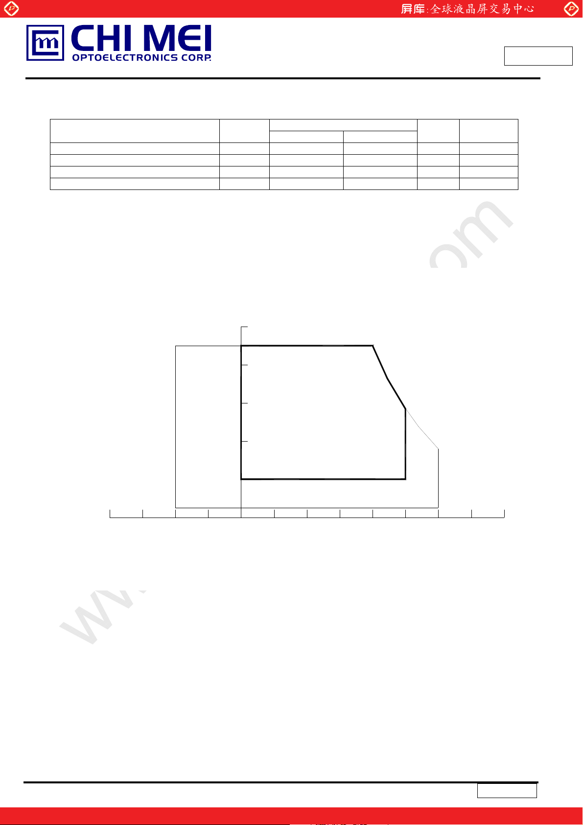
Storage Temperature TST -20 +60 ºC (1), (3)
Operating Ambient Temperature TOP 0 50 ºC (1), (2), (3)
Altitude Operating A OP 0 5000 M (3)
Altitude Storage A ST 0 12000 M (3)
Note (1) Temperature and relative humidity range is shown in the figure below.
(a) 90 %RH Max. (Ta Љ 40 ºC).
(b) Wet-bulb temperature should be 39 ºC Max. (Ta > 40 ºC).
(c) No condensation..
Min. Max.
Value
Unit Note
Approval
Relative Humidity (%RH)
100
90
80
60
Operating Range
40
20
10
Storage Range
Temperature (ºC)
8060-20 400 20-40
Note (2) The maximum operating temperature is based on the test condition that the surface temperature of
display area is less than or equal to 65 ºC with LCD module alone in a temperature controlled chamber.
Thermal management should be considered in your product design to prevent the surface temperature of
display area from being over 65 ºC. The range of operating temperature may degrade in case of improper
thermal management in your product design.
Note (3) The rating of environment is base on LCD module. Leave LCD cell alone, this environment condition can’t
be guaranteed. Except LCD cell, the customer has to consider the ability of other parts of LCD module
and LCD module process.
5
One step solution for LCD / PDP / OLED panel application: Datasheet, inventory and accessory!
Version2.0
www.panelook.com
Page 6
Global LCD Panel Exchange Center
www.panelook.com
2.2 ABSOLUTE RATINGS OF ENVIRONMENT (OPEN CELL)
Storage Condition : With shipping package.
Storage temperature range : 25±5 к
Storage humidity range : 50±10%RH
Shelf life : a month
2.3 ELECTRICAL ABSOLUTE RATINGS (OPEN CELL)
Issued Date: Feb. 23, 2009
Model No.: V315B3-P05
Approval
Item Symbol
Power Supply Voltage VDA -0.5 +14.0 V
Power Supply Voltage VGHP -0.3 +30.0 V
Power Supply Voltage VGL -10.0 -0.3 V
Logic Input Voltage VDD -0.3 +3.1 V
Note (1) Permanent damage to the device may occur if maximum values are exceeded. Function operation should
be restricted to the conditions described under Normal Operating Conditions.
Value
Min Max
Unit
Note
(1)
6
One step solution for LCD / PDP / OLED panel application: Datasheet, inventory and accessory!
Version2.0
www.panelook.com
Page 7
Global LCD Panel Exchange Center
3. ELECTRICAL CHARACTERISTICS
www.panelook.com
Issued Date: Feb. 23, 2009
Model No.: V315B3-P05
Approval
3.1 TFT LCD MODULE
Ta = 25 ± 2 ºC
Parameter Symbol
VGHP 22 23 24 V
VGL -6.0 -5.5 -5.0 V
Power Supply Voltage
VDA 13.20 13.50 13.80 V
VDD 2.4 2.5 2.6 V
VREF 12.65 12.8 12.95 V
IGH - 10 - mA
Power Supply Current
IGL - 3 - mA
IDA - 260 - mA
IDD - 225 - mA
Input High Threshold Voltage VIH 0.8VDD - VDD V CMOS
interface
Input Low Threshold Voltage V
0 - 0.2VDD V
IL
3.2 RSDS CHARACTERISTICS
Item Symbol Condition
RSDS high input
Voltage
RSDS low input
Voltage
RSDS common mode
input voltage range
RSDS Input leakage
current
Note (1) V
Note (2) V
Note (3) V
= (VCLKP + VCLKN)/2 or V
CMRSDS
DIFFRSDS
= VCLKP - VCLKN or V
= 0.8V(VDD = 2.5V)
CMRSDS
V
DIFFRSDS
V
DIFFRSDS
V
CMRSDS
I
DL
V
V
V
DIFFRSDS
D
DIFFRSDS
CMRSDS
CMRSDS
N ,CLKO ,CLPN
xx
CMRSDS
= VDXXP - VDXXN
Value
Min. Typ. Max.
Unit Note
Ta = -10~+85 ºC
Value
Min Typ Max
Unit
= +1.2 V (1) 100 200 - mV
= +1.2 V (1) - -200 -100 mV
= 200 mV (2) VSS+0.1 Note(3) VDD-1.2 V
DxxP,
-10 - 10
ӴA
= (VDXXP + VDXXN)/2
7
One step solution for LCD / PDP / OLED panel application: Datasheet, inventory and accessory!
Version2.0
www.panelook.com
Page 8
Global LCD Panel Exchange Center
4. BLOCK DIAGRAM
4.1 TFT LCD OPEN CELL
www.panelook.com
Issued Date: Feb. 23, 2009
Model No.: V315B3-P05
Approval
TFT LCD PANEL
(1366x3x768)
X(R) BOARD
RSDS SIGNAL INPUT
Connector Part No.: STARCONN 106D61-000100-A2-R or equal.
X(L) BOARD
Y BOARD
8
One step solution for LCD / PDP / OLED panel application: Datasheet, inventory and accessory!
Version2.0
www.panelook.com
Page 9
Global LCD Panel Exchange Center
www.panelook.com
Issued Date: Feb. 23, 2009
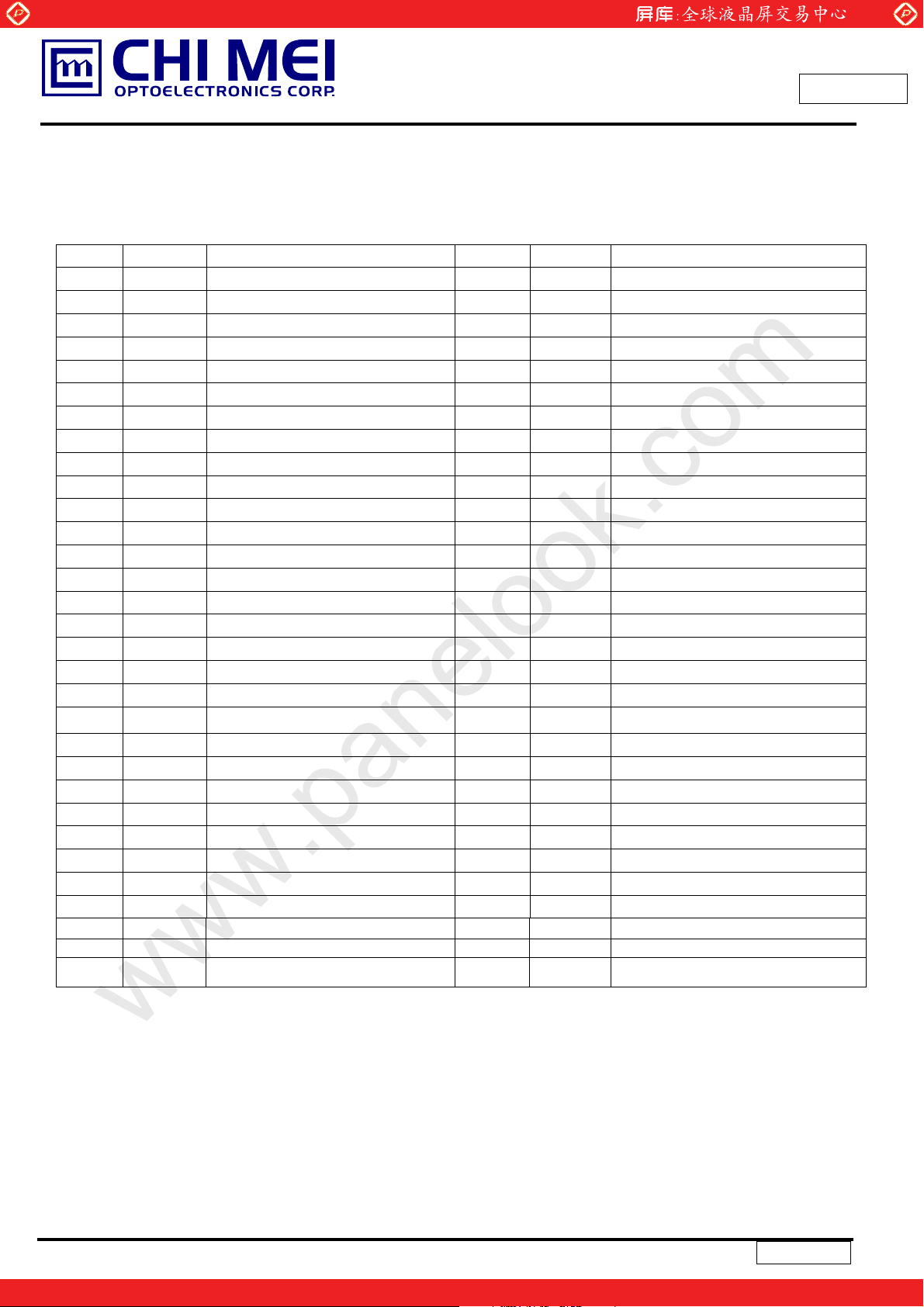
5. INPUT TERMINAL PIN ASSIGNMENT
5.1 TFT LCD MODULE
Pin assignment
CN1(XL) Connector Pin Assignment
Pin No. Symbol Description Pin No. Symbol Description
1 TR2 trace2 (3) 32 B1P
2 TR1 trace1 (2) 33 B1N
3 GND
4 GM14
5 GM13
6 GM12
7 GM11
8 GM10
9 GM9
10 GM8
11 GM7
12 GM6
13 GM5
14 GM4
15 GM3
16 GM2
17 GM1
18 VCM VCM Power supply 49 R2N
19 VDA
20
21 DRL
22 VDD
23 EIO4
24 STH
25 TP1
26 POL
27 GND
28 B3P
29 B3N RSDS data signal (Blue 3) 60 VGH Driver Power supply
30 B2P RSDS data signal (Blue 2) 61 GND Ground
31 B2N RSDS data signal (Blue 2)
VDA
Gamma Power supply
Gamma Power supply
Gamma Power supply
Gamma Power supply
Gamma Power supply
Gamma Power supply
Gamma Power supply
Gamma Power supply
Gamma Power supply
Gamma Power supply
Gamma Power supply
Gamma Power supply
Gamma Power supply
Gamma Power supply
Control the direction of start pulse
The fourth source driver start pulse
The first source driver start pulse
RSDS data signal (Blue 3)
Ground
Driver Power supply
Driver Power supply
Logic Power supply
RSDS data latch
polarity invert
Ground
34 B0P
35 B0N
36 CLKP
37 CLKN
38 G3P
39 G3N
40 G2P
41 G2N
42 G1P
43 G1N
44 G0P
45 G0N
46 R3P
47 R3N
48 R2P
50 R1P
51
52 R0P
53 R0N
54 GND
55 STV_R
56 STV
57 CKV
58 OE
59 VGL
R1N
RSDS data signal (Blue 1)
RSDS data signal (Blue 1)
RSDS data signal (Blue 0)
RSDS data signal (Blue 0)
Data driver clock
Data driver clock
RSDS data signal (Green 3)
RSDS data signal (Green 3)
RSDS data signal (Green 2)
RSDS data signal (Green 2)
RSDS data signal (Green 1)
RSDS data signal (Green 1)
RSDS data signal (Green 0)
RSDS data signal (Green 0)
RSDS data signal (Red 3)
RSDS data signal (Red 3)
RSDS data signal (Red 2)
RSDS data signal (Red 2)
RSDS data signal (Red 1)
RSDS data signal (Red 1)
RSDS data signal (Red 0)
RSDS data signal (Red 0)
Ground
Scan driver start pulse 2
Scan driver start pulse 1
Scan driver clock
Scan driver output enable
Driver Power supply
Model No.: V315B3-P05
Approval
9
One step solution for LCD / PDP / OLED panel application: Datasheet, inventory and accessory!
Version2.0
www.panelook.com
Page 10
Global LCD Panel Exchange Center
CN2(XR) Connector Pin Assignment
Pin No. Symbol Description Pin No. Symbol Description
1 GND
2 GM14
3 GM13
4 GM12
5 GM11
6 GM10
7 GM9
8 GM8
9 GM7
10 GM6
11 GM5
12 GM4
13 GM3
14 GM2
15 GM1
16 VCM VCM Power supply 47 B1P
17 VDA
18 VDA
19 VREF
20
21 STH_R
22 EIO4
23 TP1
24 POL
25 GND
26 R0N
27 R0P
28 R1N
29 R1P RSDS data signal (Red 1) 60 TR4
VDD
Gamma Power supply
Gamma Power supply
Gamma Power supply
Gamma Power supply
Gamma Power supply
Gamma Power supply
Gamma Power supply
Gamma Power supply
Gamma Power supply
Gamma Power supply
Gamma Power supply
Gamma Power supply
Gamma Power supply
Gamma Power supply
Gamma Power supply
source driver start pulse reverse
The fourth source driver start pulse
RSDS data signal (Red 0)
RSDS data signal (Red 0)
RSDS data signal (Red 1)
Ground
Driver Power supply
Driver Power supply
Logic Power supply
RSDS data latch
polarity invert
Ground
www.panelook.com
32 R3N
33 R3P
34 G0N
35 G0P
36 G1N
37 G1P
38 G2N
39 G2P
40 G3N
41 G3P
42 CLKN
43 CLKP
44 B0N
45 B0P
46 B1N
48 B2N
49 B2P
50 B3N
51
52 GND
53 DRL
54 STV
55 VSCM VSCM Power supply
56 NC No connection
57 VGL
58 NC No connection
59 GND
B3P
Issued Date: Feb. 23, 2009
RSDS data signal (Red 3)
RSDS data signal (Red 3)
RSDS data signal (Green 0)
RSDS data signal (Green 0)
RSDS data signal (Green 1)
RSDS data signal (Green 1)
RSDS data signal (Green 2)
RSDS data signal (Green 2)
RSDS data signal (Green 3)
RSDS data signal (Green 3)
Data driver clock
Data driver clock
RSDS data signal (Blue 0)
RSDS data signal (Blue 0)
RSDS data signal (Blue 1)
RSDS data signal (Blue 1)
RSDS data signal (Blue 2)
RSDS data signal (Blue 2)
RSDS data signal (Blue 3)
RSDS data signal (Blue 3)
Ground
Control the direction of start pulse
Scan driver start pulse 1
Driver Power supply
Ground
trace4 (2)
Model No.: V315B3-P05
Approval
30 R2N RSDS data signal (Red 2) 61 TR3
31 R2P
RSDS data signal (Red 2)
trace3 (3)
Note (1) CN1ΕCN2 Connector Part No.: STARCONN 106D61-000100-A2-R or equal.
Note (2) The TR1 must be connected to the TR4.
Note (3) The TR2 must be connected to the TR3.
10
One step solution for LCD / PDP / OLED panel application: Datasheet, inventory and accessory!
Version2.0
www.panelook.com
Page 11
Global LCD Panel Exchange Center
www.panelook.com
Issued Date: Feb. 23, 2009
Model No.: V315B3-P05
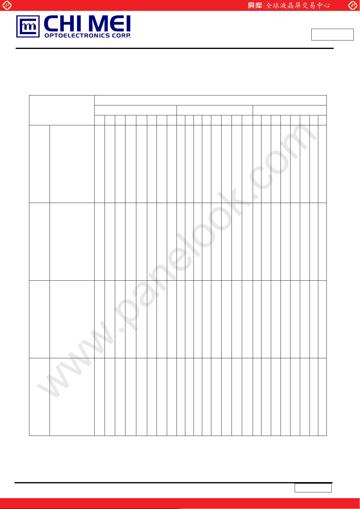
5.2 COLOR DATA INPUT ASSIGNMENT
The brightness of each primary color (red, green and blue) is based on the 8-bit gray scale data input for the color.
The higher the binary input, the brighter the color. The table below provides the assignment of color versus data
input.
Data Signal
Color
R7 R6 R5 R4 R3 R2 R1 R0 G7 G6 G5 G4 G3 G2 G1 G0 B7 B6 B5 B4 B3 B2 B1 B0
Black
Red
Green
Basic
Colors
Gray
Scale
Of
Red
Gray
Scale
Of
Green
Gray
Scale
Of
Blue
Note (1) 0: Low Level Voltage, 1: High Level Voltage
Blue
Cyan
Magenta
Yellow
White
Red(0) / Dark
Red(1)
Red(2)
:
:
Red(253)
Red(254)
Red(255)
Green(0) / Dark
Green(1)
Green(2)
:
:
Green(253)
Green(254)
Green(255)
Blue(0) / Dark
Blue(1)
Blue(2)
:
:
Blue(253)
Blue(254)
Blue(255)
0
0
1
1
0
0
0
0
0
0
1
1
1
1
1
1
0
0
0
0
0
0
:
:
:
:
1
1
1
1
1
1
0
0
0
0
0
0
:
:
:
:
0
0
0
0
0
0
0
0
0
0
0
0
:
:
:
:
0
0
0
0
0
0
Red Green Blue
0
0
0
0
0
0
0
0
0
0
0
0
0
0
0
0
0
0
0
0
1
1
1
1
1
1
0
0
0
0
0
0
0
0
0
0
0
0
0
0
0
0
0
0
0
0
1
1
1
1
1
1
1
1
0
0
0
0
0
0
0
0
0
0
0
0
0
0
0
0
0
0
0
0
1
1
1
1
1
1
0
0
0
0
0
0
1
1
1
1
1
1
1
1
1
1
1
1
1
1
1
1
1
1
1
1
0
0
0
0
0
0
0
0
1
1
1
1
1
1
1
1
1
1
1
1
1
1
1
1
1
1
1
1
0
0
0
0
0
0
1
1
1
1
1
1
1
1
1
1
1
1
1
1
1
1
1
1
1
1
0
0
0
0
0
0
0
0
0
0
0
0
0
0
0
0
0
0
0
0
0
0
0
0
0
1
0
0
0
0
0
0
0
0
0
0
0
0
0
0
0
0
0
0
1
0
0
0
0
0
0
0
0
0
0
0
0
0
0
0
:
:
:
:
:
:
:
:
:
:
:
:
:
:
:
:
:
:
:
:
:
:
:
:
:
:
:
:
:
:
:
:
:
:
:
:
:
:
:
:
1
1
1
1
0
1
0
0
0
0
0
0
0
0
0
0
0
0
0
0
1
1
1
1
1
0
0
0
0
0
0
0
0
0
0
0
0
0
0
0
1
1
1
1
1
1
0
0
0
0
0
0
0
0
0
0
0
0
0
0
0
0
0
0
0
0
0
0
0
0
0
0
0
0
0
0
0
0
0
0
0
0
0
0
0
0
:
:
:
:
:
:
:
:
:
:
:
:
:
:
:
:
:
:
:
1
0
0
0
0
0
0
1
0
0
0
0
0
0
1
0
0
0
0
0
0
0
0
0
0
0
0
0
0
0
0
0
0
0
0
0
0
0
0
0
0
0
:
:
:
:
:
:
:
:
:
:
:
:
:
:
0
0
0
0
0
0
0
0
0
0
0
0
0
0
0
0
0
0
0
0
0
:
1
1
1
1
1
1
1
1
1
0
0
0
0
0
0
0
0
0
:
:
:
:
:
:
0
0
0
0
0
0
0
0
0
0
0
0
0
0
0
:
:
:
:
1
1
1
1
1
1
0
0
0
0
0
0
:
:
:
:
0
0
0
0
0
0
0
0
1
0
0
1
:
:
1
0
0
1
1
1
0
0
0
0
0
0
:
:
0
0
0
0
0
0
0
0
0
0
0
0
0
0
:
:
:
:
:
:
0
0
0
0
0
0
0
0
0
0
0
0
:
:
:
:
:
:
1
1
1
1
1
1
0
0
0
0
0
0
0
0
:
:
:
:
0
0
0
0
0
0
0
0
0
0
0
0
:
:
:
:
1
1
1
1
1
1
0
0
0
0
0
0
:
:
:
:
0
0
0
0
0
0
0
0
0
0
0
0
:
:
:
:
1
1
1
1
1
1
Approval
0
0
0
0
0
0
1
1
1
1
1
1
0
0
1
1
0
0
0
0
0
0
:
:
:
:
0
0
0
0
0
0
0
0
0
0
0
0
:
:
:
:
0
0
0
0
0
0
0
0
0
1
1
0
:
:
:
:
0
1
1
0
1
1
11
One step solution for LCD / PDP / OLED panel application: Datasheet, inventory and accessory!
Version2.0
www.panelook.com
Page 12
Global LCD Panel Exchange Center
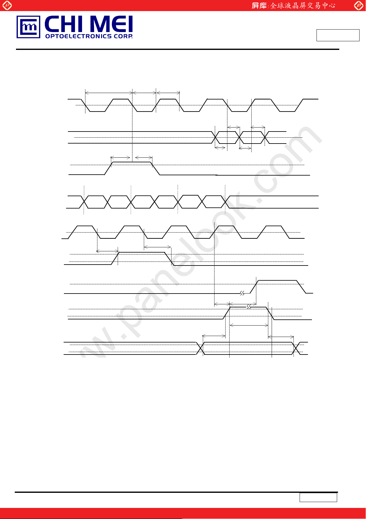
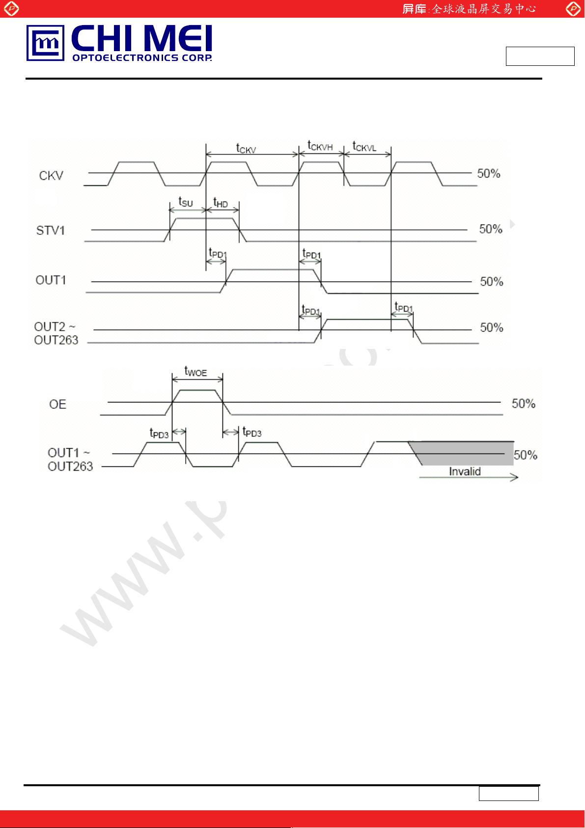
6. INTERFACE TIMING
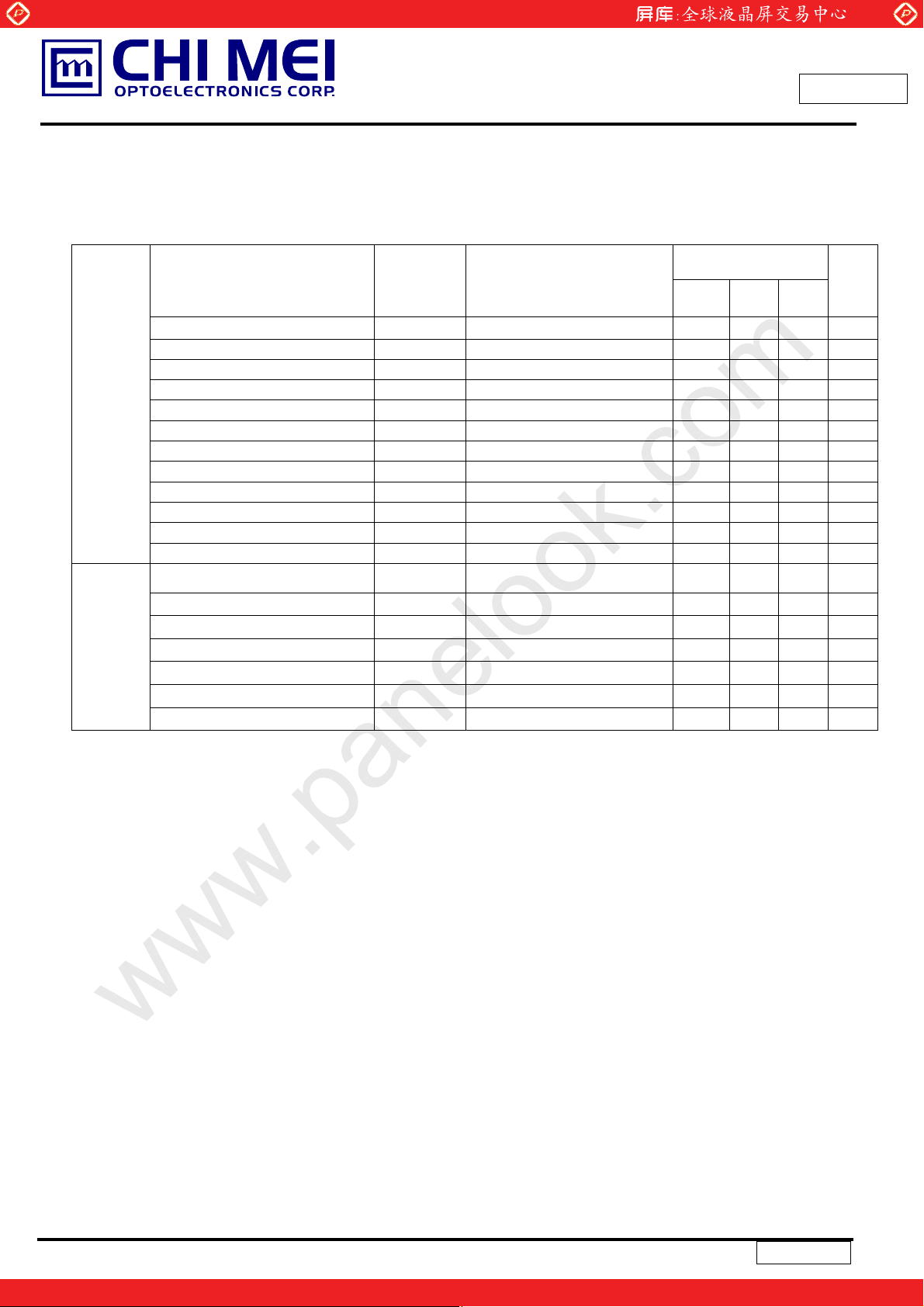
6.1 INPUT SIGNAL TIMING SPECIFICATIONS
(a) Timing Spec
Parameter Symbol Condition
www.panelook.com
Issued Date: Feb. 23, 2009
Model No.: V315B3-P05
Approval
Spec
Unit
Min. Typ. Max.
Clock pulse width t
Clock pulse low period t
Clock pulse high period t
Data setup time t
HD
Data hold time t
Start pulse setup time t
Start pulse hold time t
TP1 high period t
Last data CLK to TP1 high t
TP1 high to STH high t
POL to TP1 setup time t
TP1 to POL hold time t
CKV period
CKV pulse width
OE pulse width
VD
Data setup time
Data hold time
CKV to output delay time
OE to output delay time
Note (1) : When operation frequency=85MHz
CLK
CLK(L)
CLK(H)
SETUP1
HOLD1
SETUP2
HOLD2
TP1(H)
LAST
NEXT
POL-TP1
TP1-POL
t
CKV
!
t
CKVH, tCKVL
t
WOE
!
t
SU
!
t
HD
!
t
PD1
!
t
PD3
!
- 11.8(1) -
-
- 5 - - ns
- 5 - - ns
- 2.9 - - ns
- 2.2 - - ns
- 1.3 - - ns
- 2.2 - - ns
- 15 - - CLKP
- 1 - - CLKP
- 6 - - CLKP
POL toggle to TP1 rising 3 - - ns
TP1 falling to POL toggle 2 - - ns
- 5 -
!
50% duty cycle 2.5 -
- 1 -
- 0.5 -
- 0.5 -
CL=300pF - - 1
CL=300pF - - 0.8
ns
Ӵs
Ӵs
Ӵs
Ӵs
Ӵs
Ӵs
Ӵs
12
One step solution for LCD / PDP / OLED panel application: Datasheet, inventory and accessory!
Version2.0
www.panelook.com
Page 13
Global LCD Panel Exchange Center
%
y)
0%
(b) Horizontal Timing Chart
www.panelook.com
Issued Date: Feb. 23, 2009
Model No.: V315B3-P05
Approval
CLKP-CLKN
(RSDS)
D**P– D**N
(RSDS)
STH
(input)
D**P – D**N
(RSDS)
CLKP-CLKN
(RSDS)
EIOx
(output)
t
CLK
t
SETUP2
LAST-2
t
CLK(L)tCLK(H)
t
HOLD2
LAST-1
Even Odd Even
t
PLH1
t
PHL1
Odd
LAST
Even
t
SETUP1
Odd
t
HOLD1
t
SETUP1
Invalid Data
t
HOLD1
50%
50%
80
50%
80%
2
STH
(input)
TP1
(input)
POL
(input)
OUT
(+ → - polarity)
OUT
(- → + polarity)
RPO1/2
(+ → - polarity)
RPO1/2
(- → + polarity)
t
t
POL-TP1
LAST
t
NEXT
t
TP1(H)
Hi-Z
80%
80%
20%
t
TP1- POL
80%
20%
t
PD1 (target voltage 0.1VDDA)
t
PD2 (6-bit accuracy)
t
PD3 (target voltage 0.1VDDA)
t
13
One step solution for LCD / PDP / OLED panel application: Datasheet, inventory and accessory!
PD4 (6-bit accurac
Version2.0
www.panelook.com
Page 14
Global LCD Panel Exchange Center
(c)Vertical Timing Chart
www.panelook.com
Issued Date: Feb. 23, 2009
Model No.: V315B3-P05
Approval
14
One step solution for LCD / PDP / OLED panel application: Datasheet, inventory and accessory!
Version2.0
www.panelook.com
Page 15

Global LCD Panel Exchange Center
www.panelook.com
Issued Date: Feb. 23, 2009
Model No.: V315B3-P05
Approval
6.2 POWER ON/OFF SEQUENCE
To prevent the device from damage due to latch up , the power ON/OFF sequence shown below must be followed.
When power on : VDD Ш VGL Ш VDA Ш VGH , Input signal (t1Ї0)
When power off : Input signal , VGH Ш VDA Ш VGL Ш VDD (t2Њ0)
VGH
VDA
VSSD,VSSA
VDD
Input signal
t
t1 t2
VGL
15
One step solution for LCD / PDP / OLED panel application: Datasheet, inventory and accessory!
Version2.0
www.panelook.com
Page 16

Global LCD Panel Exchange Center
www.panelook.com
Issued Date: Feb. 23, 2009
Model No.: V315B3-P05
7. OPTICAL CHARACTERISTICS
7.1 TEST CONDITIONS
Item Symbol Value Unit
Ambient Temperature Ta
Ambient Humidity Ha
Supply Voltage V
CC
25±2
50±10
5.0 V
Input Signal According to typical value in "3. ELECTRICAL CHARACTERISTICS"
Inverter Current I
Inverter Driving Frequency F
L
L
9.50.7
663
7.2 OPTICAL SPECIFICATIONS
The relative measurement methods of optical characteristics are shown as below. The following items should be
measured under the test conditions described in 7.1 and stable environment shown in Note (5).
Item Symbol Condition Min. Typ. Max. Unit Note
Red
Green
Color
Chromaticity
Blue
White
Center Transmittance T% - 4.5 % (1), (7)
Contrast Ratio CR
Response Time
White Variation
Horizontal
Viewing Angle
Vertical
Rx
Ry 0.331
Gx
Gy 0.597
Bx
By 0.070
θ
=0°, θY =0°
x
Viewing angle at
normal direction
With CMO module
Typ.-0 .03
Wx
Wy
θ
=0°, θY =0°
x
Gray to
gray
average
δW
θx+
θ
-
x
θY+
-
θ
Y
With CMO Module
θ
=0°, θY =0°
x
With CMO
Module@60Hz
θ
=0°, θY =0°
x
With CMO Module
CR≥20
With CMO Module
1500 2500 - (1), (3)
-
1.3 - (1), (6)
80 88 80
80
80
0.641
0.272
0.144
Typ+0.03
0.280
0.290
6.5 12
88 88 88 -
o
C
%RH
mA
KHz
-
-
-
-
-
-
-
-
ms (4)
Deg. (1), (2)
Approval
(1),(5)
Note (1) Light source is CMO’s V315B3-L01 BLU and driving voltages are based on suitable gamma voltages.
Note (2) Definition of Viewing Angle (θx, θy):
Viewing angles are measured by EZ-Contrast 160R (Eldim)
16
One step solution for LCD / PDP / OLED panel application: Datasheet, inventory and accessory!
Version2.0
www.panelook.com
Page 17

Global LCD Panel Exchange Center
www.panelook.com
Issued Date: Feb. 23, 2009
Model No.: V315B3-P05
Approval
Normal
θx = θy = 0º
θy- θy+
θX- = 90º
6 o’clock
θ
y-
= 90º
x-
y-
Note (3) Definition of Contrast Ratio (CR):
The contrast ratio can be calculated by the following expression.
Contrast Ratio (CR) = L255 / L0
L255: Luminance of gray level 255
L 0: Luminance of gray level 0
CR = CR (5) ,where CR (X) is corresponding to the Contrast Ratio of the point X at the figure in Note (6).
θx−
θx+
y+
12 o’clock direction
θ
y+
= 90º
x+
θX+ = 90º
Note (4) Definition of Gray-to-Gray Switching Time:
100%
90%
Optical
Response
10%
0%
Gray to gray
Switching time
The driving signal means the signal of luminance 0%, 20%, 40%, 60%, 80%, 100%.
Gray to gray average time means the average switching time of luminance 0%,20%,
40%, 60%, 80%, 100% to each other.
Note (5) Measurement Setup:
The LCD module should be stabilized at given temperature for 60 minutes to avoid abrupt temperature
Gray to gray
Switching time
Time
17
One step solution for LCD / PDP / OLED panel application: Datasheet, inventory and accessory!
Version2.0
www.panelook.com
Page 18

Global LCD Panel Exchange Center
change during measuring. In order to stabilize the luminance, the measurement should be executed after
lighting Backlight for 60 minutes in a windless room.
LCD Module
LCD Panel
www.panelook.com
Issued Date: Feb. 23, 2009
Model No.: V315B3-P05
Approval
Center of the Screen
Note (6) Definition of White Variation (δW):
Measure the luminance of gray level 255 at 5 points
δW = Maximum [L (1), L (2), L (3), L (4), L (5)] / Minimum [L (1), L (2), L (3), L (4), L (5)]
where L (X) is corresponding to the luminance of the point X at the figure below.
Display Color Analyzer
(Minolta CA210)
Light Shield Room
(Ambient Luminance < 2 lux)
Horizontal Line
D
D/4 D/2 3D/4
12
X
5
: Test Point
X=1 to 5
W
W/4
W/2
Vertical Line
4
3W/
Note (7) Definition of Transmittance (T%):
Module is without signal input.
Luminance of LCD module
Transmittance =
Luminance of backlight
One step solution for LCD / PDP / OLED panel application: Datasheet, inventory and accessory!
34
Active Area
Ϡ 100%
18
Version2.0
www.panelook.com
Page 19

Global LCD Panel Exchange Center
X
8. DEFINITION OF LABELS
8.1 OPEN CELL LABEL
The barcode nameplate is pasted on each open cell as illustration for CMO internal control.
8.2 CARTON LABEL
The barcode nameplate is pasted on each box as illustration, and its definitions are as following explanation
www.panelook.com
Issued Date: Feb. 23, 2009
Model No.: V315B3-P05
Approval
V315B3-P05
XXXXXXXXXXXXX
(a) Model Name: V315B3– P05
P.O. NO.
Parts ID.
Carton ID. Quantities 12
XXXXXXXXXXXXXX
Made in Taiwan
(b) Carton ID: CMO internal control
(c) Quantities: 12
19
One step solution for LCD / PDP / OLED panel application: Datasheet, inventory and accessory!
Version2.0
www.panelook.com
Page 20

Global LCD Panel Exchange Center
9. PACKAGING
9.1 PACKING SPECIFICATIONS
(1) 12 LCD TV Panels / 1 Box
(2) Box dimensions : 970 (L) X 640 (W) X 319 (H)
Weight : approximately 28Kg ( 12 panels per box)
9.2 PACKING METHOD
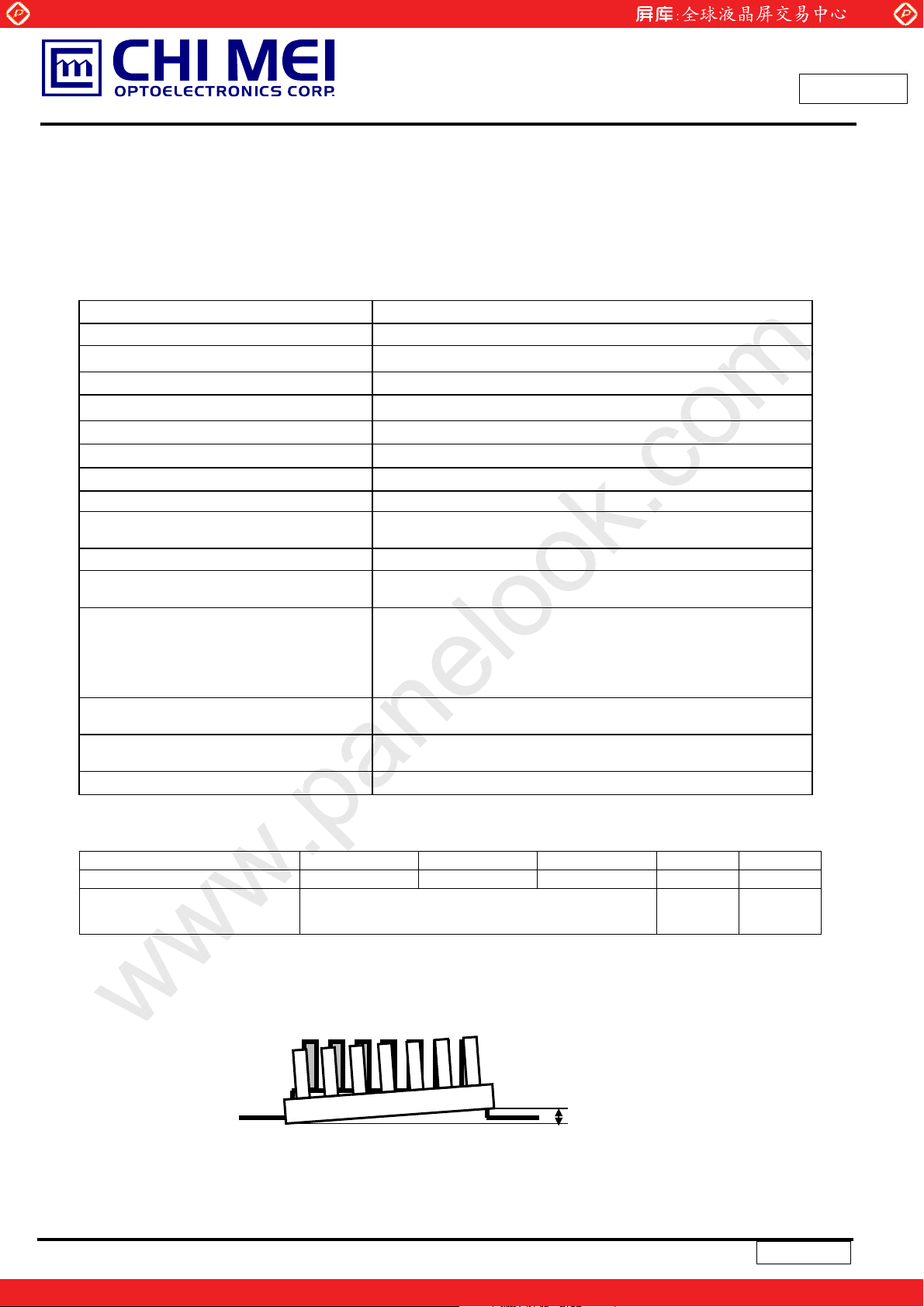
Figures 9-1 and 9-2 are the packing method
Tray need not to revolve .
LCD Panel
www.panelook.com
Tray need to revolve stack
Issued Date: Feb. 23, 2009
Model No.: V315B3-P05
Approval
The design packing t op layer for empty tray
Carton Label
Carton
Figure.9-1 packing method
20
Version2.0
One step solution for LCD / PDP / OLED panel application: Datasheet, inventory and accessory!
www.panelook.com
Page 21

Global LCD Panel Exchange Center
www.panelook.com
Issued Date: Feb. 23, 2009
Model No.: V315B3-P05
Approval
Sea Transportation
Corner Protector:L1850*50*50mm
L1130*50*50mm
Pallet:L1300*W1000*H140mm
Pallet Stack:L1300*W1000*H2054mm
Gross: 352kg
Film
PE Sheet
Carton Label
Air Transportation
Corner Protector:L1250*50*50mm
L1130*50*50mm
Pallet:L1300*W1000*H140mm
Pallet Stack:L1300*W1000*H1416mm
Gross:240kg
PE Sheet
Film
PP Belt
Carton Label
PP Belt
Figure.9-2 packing method
21
Version2.0
One step solution for LCD / PDP / OLED panel application: Datasheet, inventory and accessory!
www.panelook.com
Page 22

Global LCD Panel Exchange Center
www.panelook.com
Issued Date: Feb. 23, 2009
Model No.: V315B3-P05
Approval
10. PRECAUTIONS
10.1 ASSEMBLY AND HANDLING PRECAUTIONS
(1) Do not apply rough force such as bending or twisting to the product during assembly.
(2) To assemble backlight or install module into user’s system can be only in clean working areas. The dust and
oil may cause electrical short or worsen the polarizer.
(3) It’s not permitted to have pressure or impulse on the module because the LCD panel will be damaged.
(4) Always follow the correct power sequence when the product is connecting and operating. This can prevent
damage to the CMOS LSI chips during latch-up.
(5) Do not pull the I/F connector in or out while the module is operating.
(6) Use a soft dry cloth without chemicals for cleaning, because the surface of polarizer is very soft and easily
scratched.
(7) It is dangerous that moisture come into or contacted the product, because moisture may damage the product
when it is operating.
(8) High temperature or humidity may reduce the performance of module. Please store this product within the
specified storage conditions.
(9) When ambient temperature is lower than 10ºC may reduce the display quality. For example, the response
time will become slowly.
10.2 SAFETY PRECAUTIONS
(1) If the liquid crystal material leaks from the panel, it should be kept away from the eyes or mouth. In case of
contact with hands, skin or clothes, it has to be washed away thoroughly with soap.
(2) After the product’s end of life, it is not harmful in case of normal operation and storage.
22
One step solution for LCD / PDP / OLED panel application: Datasheet, inventory and accessory!
Version2.0
www.panelook.com
Page 23

Global LCD Panel Exchange Center
11. Mechanical Drawing
www.panelook.com
Issued Date: Feb. 23, 2009
Model No.: V315B3-P05
Approval
࡛ભሽٝڶૻֆ
CHI MEI
23
One step solution for LCD / PDP / OLED panel application: Datasheet, inventory and accessory!
Version2.0
www.panelook.com
Page 24

Global LCD Panel Exchange Center
A
TFT LCD Approval Specification
MODEL NO.:V315B3-P05
www.panelook.com
Issued Date: Feb. 23, 2009
Model No.: V315B3-P05
Approval
Customer:
pproved by:
Note:
TVHD
Approved By
LY Chen
QRA Dept. Product Development Div.
Reviewed By
Kc Ko WT Lin
LCD TV Marketing and Product Management Div.
Prepared By
Ken Wu Peter Liu
1
One step solution for LCD / PDP / OLED panel application: Datasheet, inventory and accessory!
Version2.0
www.panelook.com
Page 25

Global LCD Panel Exchange Center
www.panelook.com
Issued Date: Feb. 23, 2009
Model No.: V315B3-P05
Approval
- CONTENTS -
REVISION HISTORY
1. GENERAL DESCRIPTION
1.1 OVERVIEW
1.2 CHARACTERISTICS
1.3 MECHANICAL SPECIFICATIONS
2. ABSOLUTE MAXIMUM RATINGS
2.1 ABSOLUTE RATINGS OF ENVIRONMENT (BASED ON CMO MODULE V315B1-L01)
2.2 ABSOLUTE RATINGS OF ENVIRONMENT (OPEN CELL)
2.3 ELECTRICAL ABSOLUTE RATINGS (OPEN CELL)
3. ELECTRICAL CHARACTERISTICS
3.1 TFT LCD OPEN CELL
3.2 RSDS CHARACTERISTICS
4. BLOCK DIAGRAM
4.1 TFT LCD OPEN CELL
5. INPUT TERMINAL PIN ASSIGNMENT
5.1 TFT LCD MODULE
5.2 COLOR DATA INPUT ASSIGNMENT
6. INTERFACE TIMING
6.1 INPUT SIGNAL TIMING SPECIFICATIONS
6.2 POWER ON/OFF SEQUENCE
-------------------------------------------------------
-------------------------------------------------------
-------------------------------------------------------
-------------------------------------------------------
-------------------------------------------------------
-------------------------------------------------------
-------------------------------------------------------
3
4
5
7
8
9
12
7. OPTICAL CHARACTERISTICS
7.1 TEST CONDITIONS
7.2 OPTICAL SPECIFICATIONS
8. DEFINITION OF LABELS
8.1 OPEN CELL LABEL
8.2 CARTON LABEL
9. PACKAGING
9.1 PACKING SPECIFICATIONS
9.2 PACKING METHOD
10. PRECAUTIONS
10.1 ASSEMBLY AND HANDLING PRECAUTIONS
10.2 SAFETY PRECAUTIONS
11. MECHANICAL DRAWING
-------------------------------------------------------
-------------------------------------------------------
-------------------------------------------------------
-------------------------------------------------------
-------------------------------------------------------
16
19
20
22
23
2
One step solution for LCD / PDP / OLED panel application: Datasheet, inventory and accessory!
Version2.0
www.panelook.com
Page 26

Global LCD Panel Exchange Center
www.panelook.com
Issued Date: Feb. 23, 2009
Model No.: V315B3-P05
Approval
REVISION HISTORY
Version Date
Ver 2.0 Feb.23, 2009 All All Approval Specification was first issued.
Page
(New)
Section Description
3
One step solution for LCD / PDP / OLED panel application: Datasheet, inventory and accessory!
Version2.0
www.panelook.com
Page 27

Global LCD Panel Exchange Center
www.panelook.com
Issued Date: Feb. 23, 2009
Model No.: V315B3-P05
1. GENERAL DESCRIPTION
1.1 OVERVIEW
V315B3- P05 is a 31.5” TFT Liquid Crystal Display module. This module supports 1366 x 768 WXGA format and
can display true 16.7M colors ( 8-bit colors).
1.2 CHARACTERISTICS
CHARACTERISTICS ITEMS SPECIFICATIONS
Screen Diagonal [in] 31.51
Pixels [lines]
Active Area [mm] 697.6845 (H) x 392.256 (V) (31.51” diagonal)
Sub -Pixel Pitch [mm] 0.17025 (H) x 0.51075 (V)
Pixel Arrangement RGB vertical stripe
Weight [g] TYP. 1200 ʳ
Physical Size [mm] 716(W) x 410.8(H) x 2(D) Typ.
Display Mode Transmissive mode / Normally black
Contrast Ratio 2500:1 Typ.
Glass thickness (Array/CF) [mm] 0.7 / 0.7
Viewing Angle (CR>20) +88/-88(H),+88/-88(V) Typ.
Color Chromaticity R=(0.641, 0.331)
Cell Transparency [и]
Polarizer (CF side) Super Wide View Anti-glare coating (Haze 17%), 710.8(H) x
Polarizer (TFT side) Super Wide View, 710.8(H) x 406.6(w).
1366768
(Typical value measured at CMO’s module)
(Typical value measured at CMO’s module)
G=(0.272, 0.597)
B=(0.144, 0.070)
W=(0.280, 0.290)
(Typical value measured at CMO’s module)
4.5%Typ.
(Typical value measured at CMO’s module)
406.6(w).. Hardness: 2H
Approval
1.3 MECHANICAL SPECIFICATIONS
Item Min. Typ. Max. Unit Note
Weight 1200 g -
I/F connector mounting
position
Note (1) Please refer to the attached drawings for more information of front and back outline dimensions.
(2) Connector mounting position
The mounting inclination of the connector makes
the screen center within ±0.5mm as the horizontal.
+/- 0.5mm
4
(2)
Version2.0
One step solution for LCD / PDP / OLED panel application: Datasheet, inventory and accessory!
www.panelook.com
Page 28

Global LCD Panel Exchange Center
www.panelook.com
Issued Date: Feb. 23, 2009
Model No.: V315B3-P05
2. ABSOLUTE MAXIMUM RATINGS
2.1 ABSOLUTE RATINGS OF ENVIRONMENT (BASED ON CMO MODULE V315B1-L04)
Item Symbol
Storage Temperature TST -20 +60 ºC (1), (3)
Operating Ambient Temperature TOP 0 50 ºC (1), (2), (3)
Altitude Operating A OP 0 5000 M (3)
Altitude Storage A ST 0 12000 M (3)
Note (1) Temperature and relative humidity range is shown in the figure below.
(a) 90 %RH Max. (Ta Љ 40 ºC).
(b) Wet-bulb temperature should be 39 ºC Max. (Ta > 40 ºC).
(c) No condensation..
Min. Max.
Value
Unit Note
Approval
Relative Humidity (%RH)
100
90
80
60
Operating Range
40
20
10
Storage Range
Temperature (ºC)
8060-20 400 20-40
Note (2) The maximum operating temperature is based on the test condition that the surface temperature of
display area is less than or equal to 65 ºC with LCD module alone in a temperature controlled chamber.
Thermal management should be considered in your product design to prevent the surface temperature of
display area from being over 65 ºC. The range of operating temperature may degrade in case of improper
thermal management in your product design.
Note (3) The rating of environment is base on LCD module. Leave LCD cell alone, this environment condition can’t
be guaranteed. Except LCD cell, the customer has to consider the ability of other parts of LCD module
and LCD module process.
5
One step solution for LCD / PDP / OLED panel application: Datasheet, inventory and accessory!
Version2.0
www.panelook.com
Page 29

Global LCD Panel Exchange Center
www.panelook.com
2.2 ABSOLUTE RATINGS OF ENVIRONMENT (OPEN CELL)
Storage Condition : With shipping package.
Storage temperature range : 25±5 к
Storage humidity range : 50±10%RH
Shelf life : a month
2.3 ELECTRICAL ABSOLUTE RATINGS (OPEN CELL)
Issued Date: Feb. 23, 2009
Model No.: V315B3-P05
Approval
Item Symbol
Power Supply Voltage VDA -0.5 +14.0 V
Power Supply Voltage VGHP -0.3 +30.0 V
Power Supply Voltage VGL -10.0 -0.3 V
Logic Input Voltage VDD -0.3 +3.1 V
Note (1) Permanent damage to the device may occur if maximum values are exceeded. Function operation should
be restricted to the conditions described under Normal Operating Conditions.
Value
Min Max
Unit
Note
(1)
6
One step solution for LCD / PDP / OLED panel application: Datasheet, inventory and accessory!
Version2.0
www.panelook.com
Page 30

Global LCD Panel Exchange Center
3. ELECTRICAL CHARACTERISTICS
www.panelook.com
Issued Date: Feb. 23, 2009
Model No.: V315B3-P05
Approval
3.1 TFT LCD MODULE
Ta = 25 ± 2 ºC
Parameter Symbol
VGHP 22 23 24 V
VGL -6.0 -5.5 -5.0 V
Power Supply Voltage
VDA 13.20 13.50 13.80 V
VDD 2.4 2.5 2.6 V
VREF 12.65 12.8 12.95 V
IGH - 10 - mA
Power Supply Current
IGL - 3 - mA
IDA - 260 - mA
IDD - 225 - mA
Input High Threshold Voltage VIH 0.8VDD - VDD V CMOS
interface
Input Low Threshold Voltage V
0 - 0.2VDD V
IL
3.2 RSDS CHARACTERISTICS
Item Symbol Condition
RSDS high input
Voltage
RSDS low input
Voltage
RSDS common mode
input voltage range
RSDS Input leakage
current
Note (1) V
Note (2) V
Note (3) V
= (VCLKP + VCLKN)/2 or V
CMRSDS
DIFFRSDS
= VCLKP - VCLKN or V
= 0.8V(VDD = 2.5V)
CMRSDS
V
DIFFRSDS
V
DIFFRSDS
V
CMRSDS
I
DL
V
V
V
DIFFRSDS
D
DIFFRSDS
CMRSDS
CMRSDS
N ,CLKO ,CLPN
xx
CMRSDS
= VDXXP - VDXXN
Value
Min. Typ. Max.
Unit Note
Ta = -10~+85 ºC
Value
Min Typ Max
Unit
= +1.2 V (1) 100 200 - mV
= +1.2 V (1) - -200 -100 mV
= 200 mV (2) VSS+0.1 Note(3) VDD-1.2 V
DxxP,
-10 - 10
ӴA
= (VDXXP + VDXXN)/2
7
One step solution for LCD / PDP / OLED panel application: Datasheet, inventory and accessory!
Version2.0
www.panelook.com
Page 31

Global LCD Panel Exchange Center
4. BLOCK DIAGRAM
4.1 TFT LCD OPEN CELL
www.panelook.com
Issued Date: Feb. 23, 2009
Model No.: V315B3-P05
Approval
TFT LCD PANEL
(1366x3x768)
X(R) BOARD
RSDS SIGNAL INPUT
Connector Part No.: STARCONN 106D61-000100-A2-R or equal.
X(L) BOARD
Y BOARD
8
One step solution for LCD / PDP / OLED panel application: Datasheet, inventory and accessory!
Version2.0
www.panelook.com
Page 32

Global LCD Panel Exchange Center
www.panelook.com
Issued Date: Feb. 23, 2009
5. INPUT TERMINAL PIN ASSIGNMENT
5.1 TFT LCD MODULE
Pin assignment
CN1(XL) Connector Pin Assignment
Pin No. Symbol Description Pin No. Symbol Description
1 TR2 trace2 (3) 32 B1P
2 TR1 trace1 (2) 33 B1N
3 GND
4 GM14
5 GM13
6 GM12
7 GM11
8 GM10
9 GM9
10 GM8
11 GM7
12 GM6
13 GM5
14 GM4
15 GM3
16 GM2
17 GM1
18 VCM VCM Power supply 49 R2N
19 VDA
20
21 DRL
22 VDD
23 EIO4
24 STH
25 TP1
26 POL
27 GND
28 B3P
29 B3N RSDS data signal (Blue 3) 60 VGH Driver Power supply
30 B2P RSDS data signal (Blue 2) 61 GND Ground
31 B2N RSDS data signal (Blue 2)
VDA
Gamma Power supply
Gamma Power supply
Gamma Power supply
Gamma Power supply
Gamma Power supply
Gamma Power supply
Gamma Power supply
Gamma Power supply
Gamma Power supply
Gamma Power supply
Gamma Power supply
Gamma Power supply
Gamma Power supply
Gamma Power supply
Control the direction of start pulse
The fourth source driver start pulse
The first source driver start pulse
RSDS data signal (Blue 3)
Ground
Driver Power supply
Driver Power supply
Logic Power supply
RSDS data latch
polarity invert
Ground
34 B0P
35 B0N
36 CLKP
37 CLKN
38 G3P
39 G3N
40 G2P
41 G2N
42 G1P
43 G1N
44 G0P
45 G0N
46 R3P
47 R3N
48 R2P
50 R1P
51
52 R0P
53 R0N
54 GND
55 STV_R
56 STV
57 CKV
58 OE
59 VGL
R1N
RSDS data signal (Blue 1)
RSDS data signal (Blue 1)
RSDS data signal (Blue 0)
RSDS data signal (Blue 0)
Data driver clock
Data driver clock
RSDS data signal (Green 3)
RSDS data signal (Green 3)
RSDS data signal (Green 2)
RSDS data signal (Green 2)
RSDS data signal (Green 1)
RSDS data signal (Green 1)
RSDS data signal (Green 0)
RSDS data signal (Green 0)
RSDS data signal (Red 3)
RSDS data signal (Red 3)
RSDS data signal (Red 2)
RSDS data signal (Red 2)
RSDS data signal (Red 1)
RSDS data signal (Red 1)
RSDS data signal (Red 0)
RSDS data signal (Red 0)
Ground
Scan driver start pulse 2
Scan driver start pulse 1
Scan driver clock
Scan driver output enable
Driver Power supply
Model No.: V315B3-P05
Approval
9
One step solution for LCD / PDP / OLED panel application: Datasheet, inventory and accessory!
Version2.0
www.panelook.com
Page 33

Global LCD Panel Exchange Center
CN2(XR) Connector Pin Assignment
Pin No. Symbol Description Pin No. Symbol Description
1 GND
2 GM14
3 GM13
4 GM12
5 GM11
6 GM10
7 GM9
8 GM8
9 GM7
10 GM6
11 GM5
12 GM4
13 GM3
14 GM2
15 GM1
16 VCM VCM Power supply 47 B1P
17 VDA
18 VDA
19 VREF
20
21 STH_R
22 EIO4
23 TP1
24 POL
25 GND
26 R0N
27 R0P
28 R1N
29 R1P RSDS data signal (Red 1) 60 TR4
VDD
Gamma Power supply
Gamma Power supply
Gamma Power supply
Gamma Power supply
Gamma Power supply
Gamma Power supply
Gamma Power supply
Gamma Power supply
Gamma Power supply
Gamma Power supply
Gamma Power supply
Gamma Power supply
Gamma Power supply
Gamma Power supply
Gamma Power supply
source driver start pulse reverse
The fourth source driver start pulse
RSDS data signal (Red 0)
RSDS data signal (Red 0)
RSDS data signal (Red 1)
Ground
Driver Power supply
Driver Power supply
Logic Power supply
RSDS data latch
polarity invert
Ground
www.panelook.com
32 R3N
33 R3P
34 G0N
35 G0P
36 G1N
37 G1P
38 G2N
39 G2P
40 G3N
41 G3P
42 CLKN
43 CLKP
44 B0N
45 B0P
46 B1N
48 B2N
49 B2P
50 B3N
51
52 GND
53 DRL
54 STV
55 VSCM VSCM Power supply
56 NC No connection
57 VGL
58 NC No connection
59 GND
B3P
Issued Date: Feb. 23, 2009
RSDS data signal (Red 3)
RSDS data signal (Red 3)
RSDS data signal (Green 0)
RSDS data signal (Green 0)
RSDS data signal (Green 1)
RSDS data signal (Green 1)
RSDS data signal (Green 2)
RSDS data signal (Green 2)
RSDS data signal (Green 3)
RSDS data signal (Green 3)
Data driver clock
Data driver clock
RSDS data signal (Blue 0)
RSDS data signal (Blue 0)
RSDS data signal (Blue 1)
RSDS data signal (Blue 1)
RSDS data signal (Blue 2)
RSDS data signal (Blue 2)
RSDS data signal (Blue 3)
RSDS data signal (Blue 3)
Ground
Control the direction of start pulse
Scan driver start pulse 1
Driver Power supply
Ground
trace4 (2)
Model No.: V315B3-P05
Approval
30 R2N RSDS data signal (Red 2) 61 TR3
31 R2P
RSDS data signal (Red 2)
trace3 (3)
Note (1) CN1ΕCN2 Connector Part No.: STARCONN 106D61-000100-A2-R or equal.
Note (2) The TR1 must be connected to the TR4.
Note (3) The TR2 must be connected to the TR3.
10
One step solution for LCD / PDP / OLED panel application: Datasheet, inventory and accessory!
Version2.0
www.panelook.com
Page 34

Global LCD Panel Exchange Center
www.panelook.com
Issued Date: Feb. 23, 2009
Model No.: V315B3-P05
5.2 COLOR DATA INPUT ASSIGNMENT
The brightness of each primary color (red, green and blue) is based on the 8-bit gray scale data input for the color.
The higher the binary input, the brighter the color. The table below provides the assignment of color versus data
input.
Data Signal
Color
R7 R6 R5 R4 R3 R2 R1 R0 G7 G6 G5 G4 G3 G2 G1 G0 B7 B6 B5 B4 B3 B2 B1 B0
Black
Red
Green
Basic
Colors
Gray
Scale
Of
Red
Gray
Scale
Of
Green
Gray
Scale
Of
Blue
Note (1) 0: Low Level Voltage, 1: High Level Voltage
Blue
Cyan
Magenta
Yellow
White
Red(0) / Dark
Red(1)
Red(2)
:
:
Red(253)
Red(254)
Red(255)
Green(0) / Dark
Green(1)
Green(2)
:
:
Green(253)
Green(254)
Green(255)
Blue(0) / Dark
Blue(1)
Blue(2)
:
:
Blue(253)
Blue(254)
Blue(255)
0
0
1
1
0
0
0
0
0
0
1
1
1
1
1
1
0
0
0
0
0
0
:
:
:
:
1
1
1
1
1
1
0
0
0
0
0
0
:
:
:
:
0
0
0
0
0
0
0
0
0
0
0
0
:
:
:
:
0
0
0
0
0
0
Red Green Blue
0
0
0
0
0
0
0
0
0
0
0
0
0
0
0
0
0
0
0
0
1
1
1
1
1
1
0
0
0
0
0
0
0
0
0
0
0
0
0
0
0
0
0
0
0
0
1
1
1
1
1
1
1
1
0
0
0
0
0
0
0
0
0
0
0
0
0
0
0
0
0
0
0
0
1
1
1
1
1
1
0
0
0
0
0
0
1
1
1
1
1
1
1
1
1
1
1
1
1
1
1
1
1
1
1
1
0
0
0
0
0
0
0
0
1
1
1
1
1
1
1
1
1
1
1
1
1
1
1
1
1
1
1
1
0
0
0
0
0
0
1
1
1
1
1
1
1
1
1
1
1
1
1
1
1
1
1
1
1
1
0
0
0
0
0
0
0
0
0
0
0
0
0
0
0
0
0
0
0
0
0
0
0
0
0
1
0
0
0
0
0
0
0
0
0
0
0
0
0
0
0
0
0
0
1
0
0
0
0
0
0
0
0
0
0
0
0
0
0
0
:
:
:
:
:
:
:
:
:
:
:
:
:
:
:
:
:
:
:
:
:
:
:
:
:
:
:
:
:
:
:
:
:
:
:
:
:
:
:
:
1
1
1
1
0
1
0
0
0
0
0
0
0
0
0
0
0
0
0
0
1
1
1
1
1
0
0
0
0
0
0
0
0
0
0
0
0
0
0
0
1
1
1
1
1
1
0
0
0
0
0
0
0
0
0
0
0
0
0
0
0
0
0
0
0
0
0
0
0
0
0
0
0
0
0
0
0
0
0
0
0
0
0
0
0
0
:
:
:
:
:
:
:
:
:
:
:
:
:
:
:
:
:
:
:
1
0
0
0
0
0
0
1
0
0
0
0
0
0
1
0
0
0
0
0
0
0
0
0
0
0
0
0
0
0
0
0
0
0
0
0
0
0
0
0
0
0
:
:
:
:
:
:
:
:
:
:
:
:
:
:
0
0
0
0
0
0
0
0
0
0
0
0
0
0
0
0
0
0
0
0
0
:
1
1
1
1
1
1
1
1
1
0
0
0
0
0
0
0
0
0
:
:
:
:
:
:
0
0
0
0
0
0
0
0
0
0
0
0
0
0
0
:
:
:
:
1
1
1
1
1
1
0
0
0
0
0
0
:
:
:
:
0
0
0
0
0
0
0
0
1
0
0
1
:
:
1
0
0
1
1
1
0
0
0
0
0
0
:
:
0
0
0
0
0
0
0
0
0
0
0
0
0
0
:
:
:
:
:
:
0
0
0
0
0
0
0
0
0
0
0
0
:
:
:
:
:
:
1
1
1
1
1
1
0
0
0
0
0
0
0
0
:
:
:
:
0
0
0
0
0
0
0
0
0
0
0
0
:
:
:
:
1
1
1
1
1
1
0
0
0
0
0
0
:
:
:
:
0
0
0
0
0
0
0
0
0
0
0
0
:
:
:
:
1
1
1
1
1
1
Approval
0
0
0
0
0
0
1
1
1
1
1
1
0
0
1
1
0
0
0
0
0
0
:
:
:
:
0
0
0
0
0
0
0
0
0
0
0
0
:
:
:
:
0
0
0
0
0
0
0
0
0
1
1
0
:
:
:
:
0
1
1
0
1
1
11
One step solution for LCD / PDP / OLED panel application: Datasheet, inventory and accessory!
Version2.0
www.panelook.com
Page 35

Global LCD Panel Exchange Center
6. INTERFACE TIMING
6.1 INPUT SIGNAL TIMING SPECIFICATIONS
(a) Timing Spec
Parameter Symbol Condition
www.panelook.com
Issued Date: Feb. 23, 2009
Model No.: V315B3-P05
Approval
Spec
Unit
Min. Typ. Max.
Clock pulse width t
Clock pulse low period t
Clock pulse high period t
Data setup time t
HD
Data hold time t
Start pulse setup time t
Start pulse hold time t
TP1 high period t
Last data CLK to TP1 high t
TP1 high to STH high t
POL to TP1 setup time t
TP1 to POL hold time t
CKV period
CKV pulse width
OE pulse width
VD
Data setup time
Data hold time
CKV to output delay time
OE to output delay time
Note (1) : When operation frequency=85MHz
CLK
CLK(L)
CLK(H)
SETUP1
HOLD1
SETUP2
HOLD2
TP1(H)
LAST
NEXT
POL-TP1
TP1-POL
t
CKV
!
t
CKVH, tCKVL
t
WOE
!
t
SU
!
t
HD
!
t
PD1
!
t
PD3
!
- 11.8(1) -
-
- 5 - - ns
- 5 - - ns
- 2.9 - - ns
- 2.2 - - ns
- 1.3 - - ns
- 2.2 - - ns
- 15 - - CLKP
- 1 - - CLKP
- 6 - - CLKP
POL toggle to TP1 rising 3 - - ns
TP1 falling to POL toggle 2 - - ns
- 5 -
!
50% duty cycle 2.5 -
- 1 -
- 0.5 -
- 0.5 -
CL=300pF - - 1
CL=300pF - - 0.8
ns
Ӵs
Ӵs
Ӵs
Ӵs
Ӵs
Ӵs
Ӵs
12
One step solution for LCD / PDP / OLED panel application: Datasheet, inventory and accessory!
Version2.0
www.panelook.com
Page 36

Global LCD Panel Exchange Center
%
y)
0%
(b) Horizontal Timing Chart
www.panelook.com
Issued Date: Feb. 23, 2009
Model No.: V315B3-P05
Approval
CLKP-CLKN
(RSDS)
D**P– D**N
(RSDS)
STH
(input)
D**P – D**N
(RSDS)
CLKP-CLKN
(RSDS)
EIOx
(output)
t
CLK
t
SETUP2
LAST-2
t
CLK(L)tCLK(H)
t
HOLD2
LAST-1
Even Odd Even
t
PLH1
t
PHL1
Odd
LAST
Even
t
SETUP1
Odd
t
HOLD1
t
SETUP1
Invalid Data
t
HOLD1
50%
50%
80
50%
80%
2
STH
(input)
TP1
(input)
POL
(input)
OUT
(+ → - polarity)
OUT
(- → + polarity)
RPO1/2
(+ → - polarity)
RPO1/2
(- → + polarity)
t
t
POL-TP1
LAST
t
NEXT
t
TP1(H)
Hi-Z
80%
80%
20%
t
TP1- POL
80%
20%
t
PD1 (target voltage 0.1VDDA)
t
PD2 (6-bit accuracy)
t
PD3 (target voltage 0.1VDDA)
t
13
One step solution for LCD / PDP / OLED panel application: Datasheet, inventory and accessory!
PD4 (6-bit accurac
Version2.0
www.panelook.com
Page 37

Global LCD Panel Exchange Center
(c)Vertical Timing Chart
www.panelook.com
Issued Date: Feb. 23, 2009
Model No.: V315B3-P05
Approval
14
One step solution for LCD / PDP / OLED panel application: Datasheet, inventory and accessory!
Version2.0
www.panelook.com
Page 38

Global LCD Panel Exchange Center
www.panelook.com
Issued Date: Feb. 23, 2009
Model No.: V315B3-P05
Approval
6.2 POWER ON/OFF SEQUENCE
To prevent the device from damage due to latch up , the power ON/OFF sequence shown below must be followed.
When power on : VDD Ш VGL Ш VDA Ш VGH , Input signal (t1Ї0)
When power off : Input signal , VGH Ш VDA Ш VGL Ш VDD (t2Њ0)
VGH
VDA
VSSD,VSSA
VDD
Input signal
t
t1 t2
VGL
15
One step solution for LCD / PDP / OLED panel application: Datasheet, inventory and accessory!
Version2.0
www.panelook.com
Page 39

Global LCD Panel Exchange Center
www.panelook.com
Issued Date: Feb. 23, 2009
Model No.: V315B3-P05
7. OPTICAL CHARACTERISTICS
7.1 TEST CONDITIONS
Item Symbol Value Unit
Ambient Temperature Ta
Ambient Humidity Ha
Supply Voltage V
CC
25±2
50±10
5.0 V
Input Signal According to typical value in "3. ELECTRICAL CHARACTERISTICS"
Inverter Current I
Inverter Driving Frequency F
L
L
9.50.7
663
7.2 OPTICAL SPECIFICATIONS
The relative measurement methods of optical characteristics are shown as below. The following items should be
measured under the test conditions described in 7.1 and stable environment shown in Note (5).
Item Symbol Condition Min. Typ. Max. Unit Note
Red
Green
Color
Chromaticity
Blue
White
Center Transmittance T% - 4.5 % (1), (7)
Contrast Ratio CR
Response Time
White Variation
Horizontal
Viewing Angle
Vertical
Rx
Ry 0.331
Gx
Gy 0.597
Bx
By 0.070
θ
=0°, θY =0°
x
Viewing angle at
normal direction
With CMO module
Typ.-0 .03
Wx
Wy
θ
=0°, θY =0°
x
Gray to
gray
average
δW
θx+
θ
-
x
θY+
-
θ
Y
With CMO Module
θ
=0°, θY =0°
x
With CMO
Module@60Hz
θ
=0°, θY =0°
x
With CMO Module
CR≥20
With CMO Module
1500 2500 - (1), (3)
-
1.3 - (1), (6)
80 88 80
80
80
0.641
0.272
0.144
Typ+0.03
0.280
0.290
6.5 12
88 88 88 -
o
C
%RH
mA
KHz
-
-
-
-
-
-
-
-
ms (4)
Deg. (1), (2)
Approval
(1),(5)
Note (1) Light source is CMO’s V315B3-L01 BLU and driving voltages are based on suitable gamma voltages.
Note (2) Definition of Viewing Angle (θx, θy):
Viewing angles are measured by EZ-Contrast 160R (Eldim)
16
One step solution for LCD / PDP / OLED panel application: Datasheet, inventory and accessory!
Version2.0
www.panelook.com
Page 40

Global LCD Panel Exchange Center
www.panelook.com
Issued Date: Feb. 23, 2009
Model No.: V315B3-P05
Approval
Normal
θx = θy = 0º
θy- θy+
θX- = 90º
6 o’clock
θ
y-
= 90º
x-
y-
Note (3) Definition of Contrast Ratio (CR):
The contrast ratio can be calculated by the following expression.
Contrast Ratio (CR) = L255 / L0
L255: Luminance of gray level 255
L 0: Luminance of gray level 0
CR = CR (5) ,where CR (X) is corresponding to the Contrast Ratio of the point X at the figure in Note (6).
θx−
θx+
y+
12 o’clock direction
θ
y+
= 90º
x+
θX+ = 90º
Note (4) Definition of Gray-to-Gray Switching Time:
100%
90%
Optical
Response
10%
0%
Gray to gray
Switching time
The driving signal means the signal of luminance 0%, 20%, 40%, 60%, 80%, 100%.
Gray to gray average time means the average switching time of luminance 0%,20%,
40%, 60%, 80%, 100% to each other.
Note (5) Measurement Setup:
The LCD module should be stabilized at given temperature for 60 minutes to avoid abrupt temperature
Gray to gray
Switching time
Time
17
One step solution for LCD / PDP / OLED panel application: Datasheet, inventory and accessory!
Version2.0
www.panelook.com
Page 41

Global LCD Panel Exchange Center
change during measuring. In order to stabilize the luminance, the measurement should be executed after
lighting Backlight for 60 minutes in a windless room.
LCD Module
LCD Panel
www.panelook.com
Issued Date: Feb. 23, 2009
Model No.: V315B3-P05
Approval
Center of the Screen
Note (6) Definition of White Variation (δW):
Measure the luminance of gray level 255 at 5 points
δW = Maximum [L (1), L (2), L (3), L (4), L (5)] / Minimum [L (1), L (2), L (3), L (4), L (5)]
where L (X) is corresponding to the luminance of the point X at the figure below.
Display Color Analyzer
(Minolta CA210)
Light Shield Room
(Ambient Luminance < 2 lux)
Horizontal Line
D
D/4 D/2 3D/4
12
X
5
: Test Point
X=1 to 5
W
W/4
W/2
Vertical Line
4
3W/
Note (7) Definition of Transmittance (T%):
Module is without signal input.
Luminance of LCD module
Transmittance =
Luminance of backlight
One step solution for LCD / PDP / OLED panel application: Datasheet, inventory and accessory!
34
Active Area
Ϡ 100%
18
Version2.0
www.panelook.com
Page 42

Global LCD Panel Exchange Center
X
8. DEFINITION OF LABELS
8.1 OPEN CELL LABEL
The barcode nameplate is pasted on each open cell as illustration for CMO internal control.
8.2 CARTON LABEL
The barcode nameplate is pasted on each box as illustration, and its definitions are as following explanation
www.panelook.com
Issued Date: Feb. 23, 2009
Model No.: V315B3-P05
Approval
V315B3-P05
XXXXXXXXXXXXX
(a) Model Name: V315B3– P05
P.O. NO.
Parts ID.
Carton ID. Quantities 12
XXXXXXXXXXXXXX
Made in Taiwan
(b) Carton ID: CMO internal control
(c) Quantities: 12
19
One step solution for LCD / PDP / OLED panel application: Datasheet, inventory and accessory!
Version2.0
www.panelook.com
Page 43

Global LCD Panel Exchange Center
9. PACKAGING
9.1 PACKING SPECIFICATIONS
(1) 12 LCD TV Panels / 1 Box
(2) Box dimensions : 970 (L) X 640 (W) X 319 (H)
Weight : approximately 28Kg ( 12 panels per box)
9.2 PACKING METHOD
Figures 9-1 and 9-2 are the packing method
Tray need not to revolve .
LCD Panel
www.panelook.com
Tray need to revolve stack
Issued Date: Feb. 23, 2009
Model No.: V315B3-P05
Approval
The design packing t op layer for empty tray
Carton Label
Carton
Figure.9-1 packing method
20
Version2.0
One step solution for LCD / PDP / OLED panel application: Datasheet, inventory and accessory!
www.panelook.com
Page 44

Global LCD Panel Exchange Center
www.panelook.com
Issued Date: Feb. 23, 2009
Model No.: V315B3-P05
Approval
Sea Transportation
Corner Protector:L1850*50*50mm
L1130*50*50mm
Pallet:L1300*W1000*H140mm
Pallet Stack:L1300*W1000*H2054mm
Gross: 352kg
Film
PE Sheet
Carton Label
Air Transportation
Corner Protector:L1250*50*50mm
L1130*50*50mm
Pallet:L1300*W1000*H140mm
Pallet Stack:L1300*W1000*H1416mm
Gross:240kg
PE Sheet
Film
PP Belt
Carton Label
PP Belt
Figure.9-2 packing method
21
Version2.0
One step solution for LCD / PDP / OLED panel application: Datasheet, inventory and accessory!
www.panelook.com
Page 45

Global LCD Panel Exchange Center
www.panelook.com
Issued Date: Feb. 23, 2009
Model No.: V315B3-P05
Approval
10. PRECAUTIONS
10.1 ASSEMBLY AND HANDLING PRECAUTIONS
(1) Do not apply rough force such as bending or twisting to the product during assembly.
(2) To assemble backlight or install module into user’s system can be only in clean working areas. The dust and
oil may cause electrical short or worsen the polarizer.
(3) It’s not permitted to have pressure or impulse on the module because the LCD panel will be damaged.
(4) Always follow the correct power sequence when the product is connecting and operating. This can prevent
damage to the CMOS LSI chips during latch-up.
(5) Do not pull the I/F connector in or out while the module is operating.
(6) Use a soft dry cloth without chemicals for cleaning, because the surface of polarizer is very soft and easily
scratched.
(7) It is dangerous that moisture come into or contacted the product, because moisture may damage the product
when it is operating.
(8) High temperature or humidity may reduce the performance of module. Please store this product within the
specified storage conditions.
(9) When ambient temperature is lower than 10ºC may reduce the display quality. For example, the response
time will become slowly.
10.2 SAFETY PRECAUTIONS
(1) If the liquid crystal material leaks from the panel, it should be kept away from the eyes or mouth. In case of
contact with hands, skin or clothes, it has to be washed away thoroughly with soap.
(2) After the product’s end of life, it is not harmful in case of normal operation and storage.
22
One step solution for LCD / PDP / OLED panel application: Datasheet, inventory and accessory!
Version2.0
www.panelook.com
Page 46

Global LCD Panel Exchange Center
11. Mechanical Drawing
www.panelook.com
Issued Date: Feb. 23, 2009
Model No.: V315B3-P05
Approval
࡛ભሽٝڶૻֆ
CHI MEI
23
One step solution for LCD / PDP / OLED panel application: Datasheet, inventory and accessory!
Version2.0
www.panelook.com
 Loading...