

Page 1

Digital Audio Networking Processor
TM
CobraNet
CobraNet™ EV-2
EV-2 Development System Manual
http://www.cirrus.com
©Copyright 2005 Cirrus Logic, Inc. SEP 2005
EV-2MAN21
Page 2

CobraNet™ EV-2
A
A
A
Contacting Cirrus Logic Support
For all product questions and inquiries contact a Cirrus Logic Sales Representative.
To find the one nearest to you go to ww w.cirrus.com
IMPOR TAN T N O TICE
Cirrus Logic, Inc. and its subsidiaries ("Cirrus") believe that the information contained in this document is accurate and reliable. However, the
information is subject to change without notice and is provided "AS IS" without warranty of any kind (express or implied). Customers are
advised to obtain the latest version of relevant information to verify, before placing orders, that information being relied on is current and
complete. All products are sold subject to the terms and conditions of sale supplied at the time of order acknowledgment, including those
pertaining to warranty, indemnification, and limitation of liability. No responsibility is assumed by Cirrus for the use of this information,
including use of this information as the basis for manufacture or sale of any items, or for infringement of patents or other rights of third
parties. This document is the property of Cirrus and by furnishing this information, Cirrus grants no license, express or implied under any
patents, mask work rights, copyrights, trademarks, trade secrets or other intellectual property rights. Cirrus owns the copyrights associated
with the information contained herein and gives consent for copies to be made of the information only for use within your organization with
respect to Cirrus integrated circuits or other products of Cirrus. This consent does not extend to other copying such as copying for general
distribution, advertising or promotional purp os es, or for creating any work for resale.
CERTAIN APPLICATIONS USING SEMICONDUCTOR PRODUCTS MAY INVOLVE POTENTIAL RISKS OF DEATH, PERSONAL INJURY,
OR SEVERE PROPERTY OR ENVIRONMENTAL DAMAGE (“CRITICAL APPLICATIONS”). CIRRUS PRODUCTS ARE NOT DESIGNED,
UTHORIZED OR WARRANTED FOR USE IN AIRCRAFT SYSTEMS, MILITARY APPLICATIONS, PRODUCTS SURGICALLY
IMPLANTED INTO THE BODY, AUTOMOTIVE SAFETY OR SECURITY DEVICES, LIFE SUPPORT PRODUCTS OR OTHER CRITICAL
PPLICATIONS. INCLUSION OF CIRRUS PRODUCTS IN SUCH APPLICATIONS IS UNDERSTOOD TO BE FULLY AT THE
CUSTOMER’S RISK AND CIRRUS DISCLAIMS AND MAKES NO WARRANTY, EXPRESS, STATUTORY OR IMPLIED, INCLUDING THE
IMPLIED WARRANTIES OF MERCHANTABILITY AND FITNESS FOR PARTICULAR PURPOSE, WITH REGARD TO ANY CIRRUS
PRODUCT THAT IS USED IN SUCH A MANNER. IF THE CUSTOMER OR CUSTOMER’S CUSTOMER USES OR PERMITS THE USE
OF CIRRUS PRODUCTS IN CRITICAL APPLICATIONS, CUSTOMER AGREES, BY SUCH USE, TO FULLY INDEMNIFY CIRRUS, ITS
OFFICERS, DIRECTORS, EMPLOYEES, DISTRIBUTORS AND OTHER AGENTS FROM ANY AND ALL LIABILITY, INCLUDING
TTORNEYS’ FEES AND COSTS, THAT MAY RESULT FROM OR ARISE IN CONNECTION WITH THESE USES.
Cirrus Logic, Cirrus, the Cirrus Logic logo designs, CobraNet, and DSP Conductor are trademarks of Cirrus Logic, Inc. All other brand and
product names in this document may be trademarks or service marks of their respective owners.
SPI is a registered trademark of Motorola, Inc.
2 Rev. 2.1
Page 3

CobraNet™ EV-2
Introduction . . . . . . . . . . . . . . . . . . . . . . . . . . . . . . . . . . . . . . . . . . . . . . . . . . . . 4
Getting Started. . . . . . . . . . . . . . . . . . . . . . . . . . . . . . . . . . . . . . . . . . . . . . . . . . 6
Required Materials . . . . . . . . . . . . . . . . . . . . . . . . . . . . . . . . . . . . . . . . . . . . .6
Included: . . . . . . . . . . . . . . . . . . . . . . . . . . . . . . . . . . . . . . . . . . . . . . . . . . .6
Not Supplied: . . . . . . . . . . . . . . . . . . . . . . . . . . . . . . . . . . . . . . . . . . . . . . .6
Setup Procedure . . . . . . . . . . . . . . . . . . . . . . . . . . . . . . . . . . . . . . . . . . . . . . .6
Switch and Connector Functionality . . . . . . . . . . . . . . . . . . . . . . . . . . . . . . . .8
J300 . . . . . . . . . . . . . . . . . . . . . . . . . . . . . . . . . . . . . . . . . . . . . . . . . . . . . .8
J401 . . . . . . . . . . . . . . . . . . . . . . . . . . . . . . . . . . . . . . . . . . . . . . . . . . . . . .8
J700 . . . . . . . . . . . . . . . . . . . . . . . . . . . . . . . . . . . . . . . . . . . . . . . . . . . . . .8
P450 . . . . . . . . . . . . . . . . . . . . . . . . . . . . . . . . . . . . . . . . . . . . . . . . . . . . . .8
P501 . . . . . . . . . . . . . . . . . . . . . . . . . . . . . . . . . . . . . . . . . . . . . . . . . . . . . .8
P504 . . . . . . . . . . . . . . . . . . . . . . . . . . . . . . . . . . . . . . . . . . . . . . . . . . . . . .8
SW200 . . . . . . . . . . . . . . . . . . . . . . . . . . . . . . . . . . . . . . . . . . . . . . . . . . . .9
SW201-SW204 . . . . . . . . . . . . . . . . . . . . . . . . . . . . . . . . . . . . . . . . . . . . .9
SW500 . . . . . . . . . . . . . . . . . . . . . . . . . . . . . . . . . . . . . . . . . . . . . . . . . . . .9
Detailed Description of EV-2 Components . . . . . . . . . . . . . . . . . . . . . . . . . . 11
The Microcontroller . . . . . . . . . . . . . . . . . . . . . . . . . . . . . . . . . . . . . . . . . . . .11
Microcontroller Memory Space: . . . . . . . . . . . . . . . . . . . . . . . . . . . . . . . .11
Microcontroller Port Connections: . . . . . . . . . . . . . . . . . . . . . . . . . . . . . .12
Interfacing the Microcontroller to the CM . . . . . . . . . . . . . . . . . . . . . . . . .13
Programming the Microcontroller . . . . . . . . . . . . . . . . . . . . . . . . . . . . . . .14
Interfacing Serial Audio to the CM . . . . . . . . . . . . . . . . . . . . . . . . . . . . . . . . .15
FPGA . . . . . . . . . . . . . . . . . . . . . . . . . . . . . . . . . . . . . . . . . . . . . . . . . . . . . . .15
Configuring the FPGA . . . . . . . . . . . . . . . . . . . . . . . . . . . . . . . . . . . . . . .18
Functional Discussion of FPGA Operation . . . . . . . . . . . . . . . . . . . . . . . .18
Hex Switches . . . . . . . . . . . . . . . . . . . . . . . . . . . . . . . . . . . . . . . . . . . . . . . . .21
EV-2 Schematics, Page-by-Page Description . . . . . . . . . . . . . . . . . . . . . . . .22
Block Diagram . . . . . . . . . . . . . . . . . . . . . . . . . . . . . . . . . . . . . . . . . . . . .22
Microcontroller and Hex Switches . . . . . . . . . . . . . . . . . . . . . . . . . . . . . .22
A/D Converter . . . . . . . . . . . . . . . . . . . . . . . . . . . . . . . . . . . . . . . . . . . . .22
D/A Converter . . . . . . . . . . . . . . . . . . . . . . . . . . . . . . . . . . . . . . . . . . . . .22
Connectors and Interfaces . . . . . . . . . . . . . . . . . . . . . . . . . . . . . . . . . . . .22
Optional VCXO and clock buffers . . . . . . . . . . . . . . . . . . . . . . . . . . . . . .22
AES3 Transceiver . . . . . . . . . . . . . . . . . . . . . . . . . . . . . . . . . . . . . . . . . .22
Power Supply Conditioning . . . . . . . . . . . . . . . . . . . . . . . . . . . . . . . . . . .22
FPGA . . . . . . . . . . . . . . . . . . . . . . . . . . . . . . . . . . . . . . . . . . . . . . . . . . . .22
Appendix A: Definition of Terms . . . . . . . . . . . . . . . . . . . . . . . . . . . . . . . . . . 23
Appendix B: EV-2 Specifications . . . . . . . . . . . . . . . . . . . . . . . . . . . . . . . . . . 26
Appendix C: Other Resources . . . . . . . . . . . . . . . . . . . . . . . . . . . . . . . . . . . . 28
Appendix D: EV-2 Schematic Drawings. . . . . . . . . . . . . . . . . . . . . . . . . . . . . 29
Appendix E: EV-2 Command Line Interface.. . . . . . . . . . . . . . . . . . . . . . . . . 38
Rev. 2.1 3
Page 4
CobraNet™ EV-2
A
A
A
A
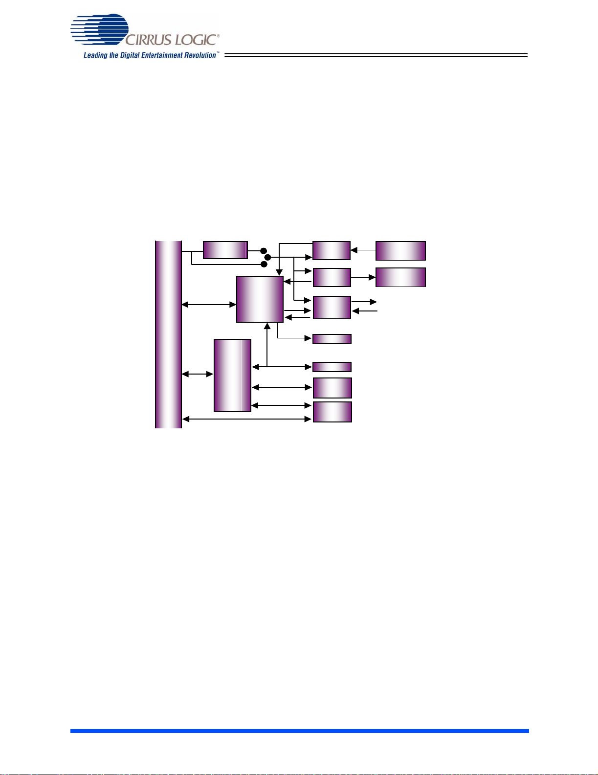
Introduction
The EV-2 provides a means of evaluatin g the CM-1 or CM-2 CobraNet™ Modu les and the Cirrus
Logic CobraNet Silicon Series of devices. In addition to evaluating the CM-1 or CM-2 (hereafter
collectively referred to as the CM except where differences between the CM-1 and CM-2 exist),
the user may also use the EV -2 as a development plat form and as an example interface for CMs,
the Cobranet Silicon Series, and other CobraNet related projects. The EV-2 connects to the CM
via the module's host interface. An 8051-type microcontroller interfaces to the CM's host port,
and a simple audio router on the EV-2 allows multiple audio inputs and outputs to connect to the
CM's serial audio interface. The EV-2 software provides a simple interface for audio routing on
the EV-2, as well as development support.
C
M
M
O
D
U
L
E
I
N
T
E
R
F
A
C
E
VCXO
8051
FPGA
DC
DAC
ES
LEDs
SRAM
Hex
Switches
RS232
Interfaces
nalog
Input
nalog
Output
Output
Input
Figure 1. EV-2 Block Diagram
Features*:
• Analog audio I/O: T wo channels of analog audio input converted to high quality, 24-bit, 48
kHz or 96 kHz digital audio. Two channels of 24-bit, 48 kHz or 96 kHz digital audio converted to high quality, analog audio output. Refer to Appendix B for audio I/O specifications.
• Digital audio I/O: One stream of AES3 input and one stream of AES3 output. An AES3
stream is two channels of digital audio. The AES3 input stream is sample rate converted.
• 8051-type microcontroller: 64kB on-chip Flash Program Memory, 1kB internal SRAM,
32kB external SRAM and in-system programmability.
• Field programmability: The supplied EV-2 software provides a means to reprogram EV-2
microcontroller firmware for field upgrades or user development.
• RS232 Interfaces: Two RS232 interfaces, one direct to the CM and another to the microcontroller.
Rev. 2.1 4
Page 5

CobraNet™ EV-2
• Routing flexibility: Route from any audio source to any audio sink using the supplied EV -2
software. Route to and from the CM as well as within the EV-2.
• Sine wave generation: A sine wave test tone may be used as an alternate audio source.
Minimal frequency and gain control is provided.
• Hex switches: Four hex formatted switches may be used for network identification of the
CobraNet module and/or user development.
• Command line interface: The 8051, via its RS232 serial interface, can be used to
configure the CM using a command line interface.Cobranet HMI variables can be vie wed
and modified using this interface. Refer to Appendix E for a description of the Command
line interface.
• LED display: Three LED indicators are provided and may be used for user development.
• Power supply: Uses standard computer ATX power supply (not included).
*The EV-2 has gone through a hardware revision to incorporate state-of-the-art A/D and D/A
converters from Cirrus logic. The new revision board is identified by a “Rev. E” designator.
Most of the changes in this document relate to the new converters and their functionality. Any
other changes which differ from the Rev. D board will be identified as such.
5 Rev. 2.1
Page 6

Getting Started
Required Materials
Included:
The CobraNet EV-2 Development Package ships with the following materials:
• EV-2 module w/ CM CobraNet PCB Qty. (2)
• 3’ CAT5 crossover cable Qty. (1)
• 6 - Pin Phoenix-style audio connectors Qty. (6)
CobraNet™ EV-2
NOTE
In order to provide you with the latest versions of our firmware and software
development kit (SDK), we use web-based distribution for our updates. To obtain
the latest versions of documentation and software, please go to
www.cirrus.com/cobranetsoftware
.
:
Not Supplied:
• Two (2) ATX computer power supplies with cables are required, one for each EV-2
module. These devices are commonly available at computer retail stores.
• Audio cables.
• RS232 cables. (Not required to pass audio.)
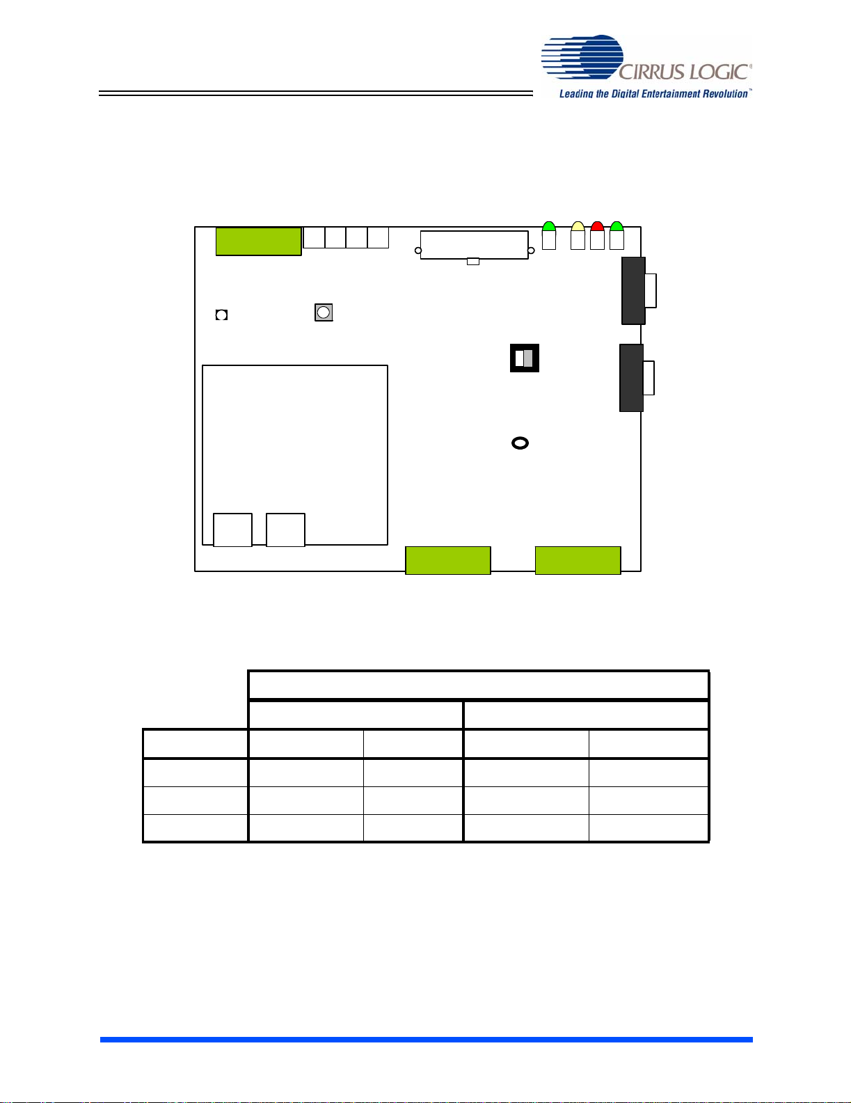
Setup Procedure
• Using the supplied Phoenix connectors, build audio input and output cables and two
AES3 cables (if desired). These will be used to connect your audio input and output
devices to the EV -2 modules. For analog audio pin assignment s, see Figure 2 or Figure 3
below. For AES3 pin assignments, see Figure 4 below.
• Connect a power supply to the ATX Power Connector at P450 on each EV-2 module.
• Connect the CAT5 crossover cable between the Ethernet jacks at J5 on each CM board.
• Connect a stereo audio source to the analog inputs at J300.
• Connect a stereo audio monitor to the analog outputs at J401.
• Apply power to both EV-2 modules.
• Verify th at you have est ablished a prope r connection. See Table 1 on page 7 for Ethernet
connector LED status The LED CR710, if on, indicates that the AES3 receiver does not
detect a valid AES3 data input stream. If AES3 I/O is not being used, this can be disregarded. Otherwise, connect a proper AES3 signal to J700. Note that there must be a valid
AES3 input for the AES3 output to work.
Rev. 2.1 6
Page 7
CobraNet™ EV-2
• CR300, when on, indicates an overflow condition detected on the A/D converter.
• The units are now ready to pass audio. The aud io input at J300 on one boa rd should now
appear at J401 on the other board and vice versa.
gnd - + gnd - +
Input Output
J700
AES I/O
CR710
AES LED
CobraNet module
CM-1 or CM-2
System Reset Switch
Hex Switches
SW201-4
SW508
P450
ATX Power Connector
Programming
Switch
SW200
CR300
Power
StatuAs
P504
Serial Bridging
Connector
P501
Serial MCU
Connector
Ethernet Jacks
J5 J6
J401
Audio Outputs
(+-gnd) (+-gnd)
J300
Audio Inputs
(+-gnd) (+-gnd)
Figure 2. Connector, Switch and Jack Locations
Module
CM-1 CM-2
Condition Left LED Right LED Left LED Right LED
Conductor Flashing Green Solid Orange Flashing Orange Flashing Green
Performer Flashing Green Solid Green Solid Orange Flashing Green
Fault Flashing Red Flashing Red Flashing Orange Flashing Orange
Table 1: Ethernet Jack Indicator Legend.
7 Rev. 2.1
Page 8
CobraNet™ EV-2
Switch and Connector Functionality
J300
Audio Input Connector: Phoenix-style connector for two-channel balanced audio input,
+14.4 dBu maximum (0 dBFS). Refer to Figure 3 for the signal connection.
J401
Audio Output Connector: Phoenix-style connector for two-channel balanced audio output,
+8.3 dBu maximum (0 dBFS). Refer to Figure 3 for the signal connection.
+ -
Left
Figure 3. Analog Audio Input and Output Phoenix-style Connectors
gnd
+ -
Right
gnd
J700
AES3 I/O Connector: Phoenix-style connector for an AES3 stream. Refer to Figure 4 for the
signal connection. For the AES3 tranceiver to operate properly a vailid AES3 signal must be
provided at the AES3 input.
+ - gnd
Figure 4. AES3 I/O Phoenix-style Connector
Output
+ - gnd
Input
P450
ATX power supply connector: ATX power supply is not included with this kit.
P501
9-Pin, D-Type Conne ctor: RS232 connection for communicating with the EV-2 microcontroller
using the supplied routing software or a command line interface ( see Appendix E ). Data
format is 19200, e, 8, 1.
P504
9-Pin, D-Type Connector: RS232 connection to the CM for serial bridging. The default data
format is 19200 baud, 9-bit format for the CM-1. 9-bit format supports any 8 bit format with
parity such as 19200, e, 8, 1. The default data format for the CM-2 is 19200 baud, 8-bit
format.
Rev. 2.1 8
Page 9

CobraNet™ EV-2
SW200
Programming switch: The EV-2 microcontroller can be programmed via its serial port,
connector P501. The supplied software can be used to perform field updates to the board's
code and firmware. This programming capability is initially disabled, but can be enabled by
setting the hex switches to FFF8H and then clicking on the "Hex Switches" display (see
Figure 6 ). For more information about the programming mode, please refer to the
Programming the Microcontroller section.
SW201-SW204
Hex switches: SW201-SW204 may be used to uniquely identify the unit on a network. Valid
settings fall within the range 0000-FFEF (values FFF0-FFFF are reserved). Changing these
values updates the value of the CobraNet module's SNMP variable, sysName, to the current
hex switch value. Through SNMP, the user may query this variable. The SNMP response is of
the form "PEAK_AUDIO_EVAL-SWwxyz", where the wxyz represents the hex values of the
switches in ASCII format.
SW500
System reset switch: This momentary switch resets the EV-2 and attached CM, and initiates
calibration operations for the analog-to-digital converter (ADC) and digital-to-analog
converter (DAC).
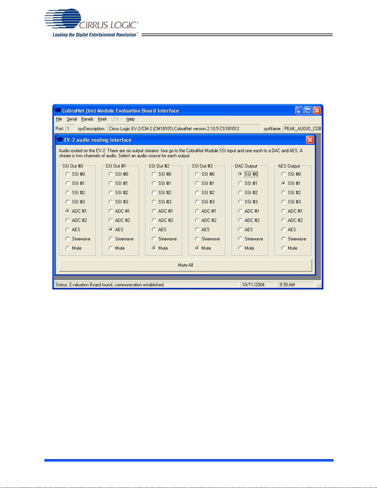
Software
The EV-2 is supplied with the CNEval.exe application, which may be used to setup audio routes
on the EV-2 (this should not be confused with routing audio over the CobraNet network). The
EV-2 has seven sources of audio input, with each source consisting of a stereo pair of audio
channels. The sources are:
• Four Synchronous Serial Interface (SSI) audio streams from the CM
• An AES3 audio input stream.
• One audio stream from the ADC (Rev. D boards had two audio streams from the ADC)
• A sine wave generator, a stream of two identical 24-bit resolution sine waves.
Using CNEval.exe, the user can route any of these seven source streams to any of the six output
streams. The available output streams are:
• The four SSI audio streams going to the CM
• One going to the DAC
• One to the AES3 transmitter.
CNEval.exe communicates with the EV-2 via an RS-232 serial connection. CNEval.exe can
communicate using either COM1 or COM2 of the PC on which it is running. The connection from
computer to EV-2 must be made as follows:
• Connect a straight-through, male-to-female, 9-pin RS232 cable to EV-2 connector P501.
9 Rev. 2.1
Page 10
CobraNet™ EV-2
• Select the appropriate PC serial port. The software will attempt to make contact with the
EV-2.
• Once communication is established, the routing can then be configured. (See Figure 5
below for an example of a routing scheme.)
Figure 5. Screen Shot of EV-2 Software - Audio Routing Interface
The default on power up state of the EV-2 is for the ADC and DAC to be the source and sink
respectively, using the CM’s SSI #0 I/O stream. The audio is then transmitted/received via a
CobraNet Bundle to/from the other CM. This allows evaluation of the CobraNet module in the
analog domain without any configuration.
The EV-2 software also has a programming mode that may be used to perform field updates of
the EV-2 microcontroller code. For more information about the programming mode, please refer
to the section Programming the Microcontroller below.
Besides the Route panel, the HMI panel under the Panels menu allows the user to configure
some HMI variables for evaluation purposes. From the HMI panel the user can set receiver and
transmitter bundle assignments as well as changes latency, data format, and sample rate.
The Peek menu provides a means to view HMI variables. In the various panels under Peek,
items that are in an indented text field are ones which are read/write. These can not be changed
from the Peek panels but are there to alert the user that these are variables that could be
changed via SNMP or the Host port.
Rev. 2.1 10
Page 11
CobraNet™ EV-2
Detailed Description of EV-2 Components
The Microcontroller
The microcontroller on the EV-2 is a Philips Semiconductor P89C51RD2. This microcontroller
has 64 kByte of internal Flash Program Memory and 1 kByte of Static RAM. The microcontroller
is field programmable using the provided CNEval.exe software. The microcontroller's clock rate
is 33Mhz. Philips P89C51RD2 preliminary specification for programming information and part
usage may be found on the Philips Semiconductor website:
http://www.semiconductors.philips.com
Microcontroller Memory Space:
Besides the internal program and data memory space the microcontroller also has an
external 64k data memory space. The microcontroller is hard-wired to execute from internal
Flash Program Memory only. The Flash Program Memory has been segmented to store both
Program and FPGA configuration data. The Program Memory map is shown in Table 2 on
page 11 and the data memory map is shown in Table 3 on page 11:
Memory Location Description
.
0x0000-0xBFFF Program Memory
0xC000-0xFFFF FPGA Configuration Data
Table 2: Flash Program Memory Map
Memory Location Description
0x0000- 0x02FF Internal Static RAM
0x0300-0x7FFF External Static RAM
0x8000-0x87FF Unused
0x8800 FPGA express mode con-
figuration*
0x8801-0xFFFF Unused
Table 3: Microcontroller Data Memory Map After Reset but Before FPGA
Configuration
*After reset, the FPGA is the only device in the upper 32k of the data memory space. The
microcontroller is then able to configure the FPGA and once configured the FPGA performs
more sophisticated address decoding of the upper data memory space. Refer to the FPGA
section of this document for a detailed description of the configuration process and a listing of
the current EV-2 FPGA firmware memory map.
11 Rev. 2.1
Page 12

CobraNet™ EV-2
Microcontroller Port Connections:
Port 0: used for the address/data (AD) bus. Once configured, the FPGA latches the lower
address byte from the AD lines.
Port 1: used for several purposes as shown in Table 4 on page 12.
Bit # Name of Signal I/O Description
0 INIT_IO# I Used when configuring the FPGA.
Refer to Xilinx Spartan datasheet
for more detail.
1 PROGRAM# O Used to initiate the FPGA configu-
ration. Refer to Xilinx Spartan
datasheet for more detail.
2 MUTE# I Mute signal from the CM module
3 HEX_DATA_IN O Not used. May be used to concat-
enate settings from other hex
switches.
4 HEX_CLOCK O Used to latch the hex switch val-
ues into a serial shift register.
5 HEX_SHIFT O Used to shift the hex switch values
from the serial shift register.
6 HEX_DATA_OUT O The hex switch value from the
serial shift register appears at this
input.
7 MCU_P17 O This is used for communication
between the FPGA and MCU.
Table 4: Port 1 Signal Descriptions
Port 2: upper address bus. Port 2 is output only.
Rev. 2.1 12
Page 13

CobraNet™ EV-2
Port 3: See Table 5 on page 13.
Bit # Name of Signal I/O Description
0 RXD I RS232 serial port receive signal.
1 TXD O RS232 serial port transmit signal
2 HREQ# O Connected to the CM module host
request signal. See CobraNet
Technical Datasheet for a com-
plete description of this signal.
3 HACK# I Connected to the CM module host
acknowledge signal. See Cobra-
Net Technical Datasheet for a
complete description of this signal.
May be used as an interrupt
request on the microcontroller.
4 Watchdog I Watchdog signal from the CM
5 MCU_P35 I/O Connected to SCI_CLK via the
FPGA. Also used to detect sample
rate.
6 WR# O Microcontroller write signal.
7 RD# O Microcontroller read signal.
Table 5: Port 3 Signal Descriptions
Interfacing the Microcontroller to the CM
Please refer to the EV-2 schematic, found in Appendix D for information regarding interfacing
to the CM.
The CM has a host interface that allows a host processor (such as an 8051 microcontroller)
to interface to the DSP on the CM. From a hardware perspective the interface to the CM-1
and CM-2 is almost the same,. The host interface signals are a data strobe signal, HDS#; a
read/write line, HRW, an 8-bit bi-directional data bus, HD0-HD7, and three address lines,
HA0-HA2 on the CM-1 and four address lines, HA0-HA3 on the CM-2. The HEN# line has
been configured by the CobraNet software to be ignored or seen as a logic low. Given this
host configuration, the interface of the microcontroller to the CM host port is straightforward.
In addition to the above signals there are two more, HACK# and HREQ# which can be used
as flags to indicate a state change on the CM.
With regard to the CM-1 which uses a Motorola DSP56303, care must be taken with the
timing of HDS# and HWR. Motorola's timing specifications for the DSP56303 host port in a
non-multiplexed, single data strobe mode requires a set up time from the falling edge of
HWR# to the falling edge of HDS# of 4.7ns and the hold time from the rising edge of HDS# to
the rising edge of HWR# of 3.3ns. The pulse of the HDS# signal must be wholly within the
pulse of the HWR# signal with the constraints stated above. Please refer to Motorola's
DSP56303 Technical Data sheet for complete information regarding timing and interface
issues. This is available for download from the Motorola web site at
http://www.freescale.com
.
13 Rev. 2.1
Page 14

CobraNet™ EV-2
In the EV-2 application, the host address lines are generated by the address latch in the
FPGA (see Table 6 on page 16) and the host data bus is connected directly to the data b us of
the microcontroller . The HREQ# and HACK# signals are connected to the two inte rrupt inputs
of the microcontroller. These signals may be used for data handshaking and asynchronus
notification respectively.
The final host signal, HRESET#, resets the CM when asserted low. Setting a bit in the host
reset register (see Table 6 on page 16) controls this signal. See the discussion of the FPGA
below for more information about this signal.
Supplemental information regarding the CM Host interface may by found in the section titled
"Host Management Interface" in the CS1810xx data sheet available on the Cirrus Logic
website: www. cirrus.com.
Programming the Microcontroller
The EV-2 is design ed so that field updates of b oth the microcontroller firmwa re and the FPGA
firmware are possible. If only the efficacy and performance of the CobraNet paradigm is
being evaluated, reprogramming of the microcontroller is not required. However, use of the
field program capability may aid in the design of a CobraNet based product.
Modifying the Flash Program Memory of the microcontroller constitutes the update.
The programming instructions that follow pertain to the supplied EV-2 routing/programming
software, CNEval.exe. Programming the microcontroller is a multi-stage process:
1. Install the EV-2 CNEval.exe software on your Windows-based computer.
2. Install an RS232 cable from port 1 or 2 on your PC to P501, the 9-pin D-type connector closest to the center of the board.
3. Run CNEval.exe
4. Change the hex switches (SW201-SW204) to FFF8 (as viewed when looking at the
hex switches). You may, as an alternative, click in the narrow recessed panel on the
left of the upper status bar.
5. Select "Program" from the Utility menu in CNEval.exe.
6. From the “Serial” drop-down menu select a serial connection, either port COM1 or
COM2 based on which is connected.
7. Located near the two serial RS232 connectors is a switch, SW200. This switch must
be set to the program mode position. The program position is indicated by silk screen
on the EV-2 board.
8. Push switch SW508, the momentary reset switch. SW508 is located just behind the
hex switches.
9. Select which firmware to update, either the FPGA or the 8051.
10. Wait for programming to complete. Do not interrupt the programming process!
11. Once programming has completed for the microcontroller or the FPGA firmware,
return the programming switch, SW200, to the normal operation position and press
the reset switch, SW508.
12. Click OK to return to the main window in CNEval.exe.
Rev. 2.1 14
Page 15

CobraNet™ EV-2
Interfacing Serial Audio to the CM
In general, interfacing to most off-the-shelf A/D and D/A converters is straight forward and the CM
is no exception. Most signals for a direct connection to these as well as other audio ICs such as
the CS8420 AES3 transceiver, are available on the CM module interface connector. Most
converters provide for a choice of bit clock and sample (frame) clock polarity, as well as audio
data formats such as SPI™ or I2S.
The A/D converter, a Cirrus Logic CS5381 is configured for slave operation, which means that it
requires a bit clock and a sample (frame) clock input. The master, bit and sample clocks are
direct connections from FS512, SCK and FS1 respectively, as is the data stream which comes
from one of the SSI ports. The CM can be configured to clock data from either edge of the bit
clock, as well as allowing for specifying the polarity of the sample clock. (See the CobraNet
website and the CobraNet Technology Datasheet for more information.) This is important since
the CS5396 works with sample pairs which need to be phase aligned. The polarity of the sample
clock specifies this alignment. For the EV-2 application, the SSI ports of the CM have been
programmed to send two channels per port. This allows a straightforward connection without any
demultiplexing.
The connection to the Cirrus Logic CS4398 D/A converter is similarly straightforward. Like the
SCS5381, it uses the FS512, bit clock and sample clock directly from the CM. Data to the DAC
and from the ADC are also direct except that they pass through a selector circuit in the FPGA. If
a particular design does not include multiple sources of audio, then the connection can be direct
to the CM interface connector.
FPGA
The Field Programmable Logic Array is a Xilinx Spartan(tm) XCS10XL VQ100-4. I t is mapped into
the microcontroller's memory space. The microcontroller must configure the FPGA after power
on or reset. Express mode configuration is used for this part. Refer to the Xilinx Spartan(tm) XL
family data sheet for more information on the Express mode configuration operation. This data
sheet can be found at the Xilinx web site, http://www.xilinx.com/. The address for configuration is
0x8800. Once configured, the FPGA's two main functions are to decode the microcontroller's
address signals and to route audio from a user selected source to a user selected destination.
Secondary functions are to generate a sine wave signal and implement registers whose function
are mostly of a control nature. A discussion of the memory decoding, routing, sine wave
generation and other functions follow.
The memory map of the upper 32k of the microcontroller space after configuration, is shown in
Table 6 on page 16. Most bit-defined locations use the least significant microcontroller data bus
signal AD0 as the controlling bit. Other data bits are ignored on these registers. Power on and
reset default for all registers is 0 unless specified otherwise.
15 Rev. 2.1
Page 16

CobraNet™ EV-2
Memory
Location
0x8000 W Bit register for green LED, CR903. 0=LED on, 1=LED off.
0x8001 W Bit register for red LED, CR904. 0=LED on, 1=LED off.
0x8002 W Bit register for yellow LED, CR905. 0=LED on, 1=LED off.
0x8004 W Bit register for green LED blink control. 0=blink off, 1=blink
0x8005 W Bit register for green LED blink control. 0=blink off, 1=blink
0x8006 W Bit register for green LED blink control. 0=blink off, 1=blink
0x8008 W DAC audio routing address (see Table 7 on page 18).
0x8009 W Bit register for DAC mute signal. 0=mute on, 1=mute off.
0x800A W Bit register for sample rate mode. 0=48k, 1=96k. Note: use
R/W Description
Refer to Table 10 on page 20 for this and other LED registers.
on.
on.
on.
AD1 instead of AD0
0x800B W Bit register for DAC reset signal. 0=reset on, 1=reset off.
0x8010 R Audio Calibration Status. 1=Calibrating, 0=Ready. See the
Calibrating Audio section for details.
0x8010 W Manual ADC Calibration. 0=Normal, 1=Calibrate. See the
Calibrating the ADC section for details. (Rev. D applicable
only)
0x8011 W Bit register for ADC slave/master control. 0=Slave, 1=Mas-
ter. (Rev. D applicable only)
0x8012 W ADC high pass filter (HPF) select. 0=Enabled, 1=Disabled.
0x8018 W AES3 audio routing address (see Table 7 on page 18).
0x8019 W Bit register for AES3 mute signal. 0=AES output muted,
1=Unmuted.
0x8020 W SSI 0 audio routing address (see Table 7 on page 18).
0x8021 W Bit register for SSI 0 mute signal. 0=Muted, 1=Unmuted.
0x8028 W SSI 1 audio routing address (see Table 7 on page 18).
0x8029 W Bit register for SSI 1 mute signal. 0=Muted, 1=Unmuted.
Table 6: Microcontroller Memory Map of Upper 32k After FPGA Configuration
Rev. 2.1 16
Page 17

CobraNet™ EV-2
Memory
Location
0x8030 W SSI 2 audio routing address (Table 7 on page 18).
0x8031 W Bit register for SSI 2 mute signal. 0=Muted, 1=Unmuted.
0x8038 W SSI 3 audio routing address (Table 7 on page 18).
0x8039 W Bit register for SSI 3 mute signal. 0=Muted, 1=Unmuted.
0x8040 Note 1 CM-1 Host Port ICR register. CM-2 Message-A register.
0x8041 Note 1 CM-1 Host Port CVR register. CM-2 Message-B register.
0x8042 Note 1 CM-1 Host Port ISR register. CM-2 Message-C register.
0x8043 Note 1 CM-1 Host Port IVR register. CM-2 Message-D register.
0x8044 Note 1 CM-1: Unused. CM-2 Data-A register.
0x8045 Note 1 CM-1 Host Port Data register high. CM-2 Data-B register.
0x8046 Note 1 CM-1 Host Port Data register middle. CM-2 Data-C register.
0x8047 Note 1 CM-1 Host Port Data register low. CM-2 Data-D register.
0x8048 Note 1 CM-2 Host Control Register.
R/W Description
0x8049 Note1 CM-2 Host Status Register.
0x8051 W Bit register for Host reset signal. 0=Asserted, 1=Deas-
serted.
0x8052 W Bit register for Host interface mode. 0=Motorola, 1=Intel
0x8054 W Signal MCU_P35 is either SCI_CLK from the CM or FS1
from the CM. 0=SCI_CLK, 1=FS1.
0x8058 R/W Auxiliary lines. Not used, for test purposes only.
0x8060 R FPGA configuration major version.
0x8061 R FPGA configuration minor version.
0x8062 R FPGA configuration revision number.
0x8070 R/W Sinewave Gain register. See Table 9 on page 19.
0x8078 R/W Sinewave Frequency register. See Table 8 on page 19.
Table 6: Microcontroller Memory Map of Upper 32k After FPGA Configuration
Note 1: The FPGA only decodes this address. The actual register is located on the CM. See the
Motorola DSP56303 users manual or the CS18101 manual for a discussion of each of these host
port registers.
17 Rev. 2.1
Page 18

CobraNet™ EV-2
Configuring the FPGA
The FPGA is configured from data that is stored in the upper 16kbytes (0xC000-0xFFFF) of
the microcontroller’s Flash Program Memory. The microncontroller code for configuring the
FPGA uses express mode which writes byte-wide data to the FPGA. Refer to the Xilinx
Spartan XL family data sheet for more information on the express mode configuration
operation. The address used for writing configuration data is 0x8800.
Functional Discussion of FPGA Operation
Routing of Audio Data
The routing of audio data is achieved by a simple 8 to 1 multiplexing operation; for each
audio destination three data bits in an a register in the FPGA select the source. For
example, the three data bits in the D/A audio routing register determine which audio
source is selected to appear at the analog outputs (J401). Table 7 on page 18 shows the
definition of the data bits and the respective audio source.
microcontroller data bit
AD2 AD1 AD0
000CM SSI 0
001CM SSI 1
010CM SSI 2
011CM SSI 3
100ADC
1 0 1 AES3 Input
1 1 0 ADC (low latency, Rev D only)
Otherwise same as ADC above.
111Sine wave
Audio Source
Table 7: Definition of Audio Routing Register Bits
Rev. 2.1 18
Page 19

CobraNet™ EV-2
Sine Wave Generator
The FPGA contains a 32-sample, 24-bit, sine table. The table is stepped through at the
sample clock rate so the resulting fundamental frequency is 48kHz / 32 samples =
1500Hz and 3000Hz at 96kHz. Limited control over frequency and gain is provided.
Listed below are the values to write to the frequency and gain registers in the FPGA.
Frequency register data bits
Frequency
48kHz sample rate
AD3 AD2 AD1 AD0
0 0 0 1 1.5 kHz (3.0 kHz)
0 0 1 0 3.0 kHz (6.0 kHz)
0 0 1 1 4.5 kHz (9.0 kHz)
0 1 0 0 6.0 kHz (12.0 kHz)
0 1 0 1 7.5 kHz (15.0 kHz)
0 1 1 0 9.0 kHz (18.0 kHz)
0 1 1 1 10.5 kHz (21.0 kHz)
1 0 0 0 12.0 kHz (24.0 kHz)
(96kHz sample rate)
Table 8: Sine Wave Frequency Register Bit Definitions
Gain register data bits
AD1 AD0
000dB
Gain
0 1 -6dB
1 0 -12dB
1 1 -18dB
Table 9: Sine Wave Gain Register Bit Definitions
19 Rev. 2.1
Page 20
CobraNet™ EV-2
LED Control
There are two bit registers to control the state of each of three LEDs. The mapping of
control bits to LED behavior is described in Table 10 on page 20. The data bit is always
AD0. Note that blink overrides on/off but when blink is turned off the LED will go to the
state designated by the On/Off bit.
On/Off Blink Status
00off
10on
01blink
11blink
Table 10: LED Status
Calibrating the ADC
There is a ten-second warm-up time to allow both the ADC and DAC to settle. All audio is
muted during this 10-second warm-up. This warm-up cycle only takes place on system
reset which is initiated by either power-up or a user pushing the reset button (SW508).
Version Control
The FPGA contains three hardwired eight-bit registers that contain an ASCII version
number of the FPGA configuration file. The microcontroller reads these registers for
version control and reporting purposes.
Mute Control
Muting comes from three different sources 1) the microcontroller can mute or unmute
audio by writing to a bit control register. There is one mute bit control register for each
output audio path, 2) the CM asserts its mute signal, and 3) all audio is unconditionally
muted during a power on/reset warm-up cycle.
Rev. 2.1 20
Page 21

CobraNet™ EV-2
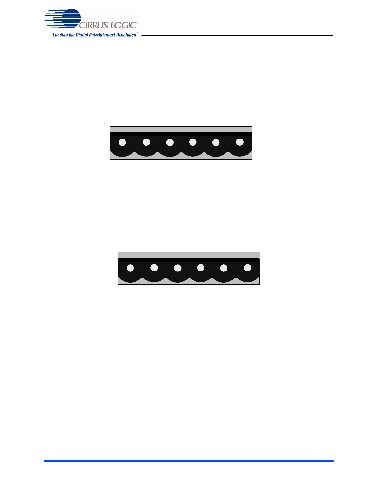
Hex Switches
Four pins on the 8051 allow the hex switches to be read. The EV-2 circuitry associated with the
hex switches serves as an example implementing this common CobraNet feature (see
Recommended User Interface Practices section in the CobraNet Programmer’s Manual for a
discussion of use of this scheme). Requirements include a physical (hardware) mapping of the
hex switches to a code (software) within the CM. Some of the requirements to achieve this are
listed below:
1. Two of the four signals will be control signals: a Shift/Load# signal where Shift is hig h
and Load is Low . The Load allows for p arallel, asynchronous loading of the hex switch
data into a shift register and the Shift allows for serial shifting of data out of that register. A clock signal to perform the shifting operation where data changes on the rising
end of the clock. The 74HC165 IC is an example of a part that supports this protocol.
2. The other two signals are the shifted data output and an input that will be shifted serially into the shift register concatenating it with the hex data. The intent of this latter
signal is to allow for the possibility of concatenating other data, additonal hex switches
or otherwise, for application specific enhancements.
3. The software will convert the serial hex data stream to a four-byte ASCII value that
represents the switch settings.
Figure 6. Example Switch Setting
As shown in Figure 6, viewing hex switches from the front, the given switch positions would read
as "CA30" in a software query of the hex switch setting. On the EV-2, the microcontoller is
responsible for reading the switches through the hardware serial interface and converting those
readings to an ASCII representation. This representation is then written to the CM through the
host port. Specifically, the EV-2 microcontroller updates the CM's HMI variable, sysName. Using
SNMP, the user may query this variable. The SNMP response is of the form
"PEAK_AUDIO_EVAL-SWwxyz", where the wxyz represents the hex values of the switches in
ASCII format. In the example shown in Figure 6, a query of sysName would return
"PEAK_AUDIO_EVAL_SWCA30".
21 Rev. 2.1
Page 22

CobraNet™ EV-2
EV-2 Schematics, Page-by-Page Description
The following sections provide detailed descriptions of the EV-2 schematic drawings contained in
Appendix D.
Block Diagram
This page is a hierarchical block diagram showing an overview of all schematic pages and
interconnects between pages.
Microcontroller and Hex Switches
This page shows an 8051-type microcontroller, its connections, and peripherals. Peripherals
include 32kbytes of SRAM, hex switch interface, clock oscillator and programming switch.
A/D Converter
This circuit is based on the Cirrus Logic CS5381 reference design. See the Cirrus Logic
website, http://www.cirrus.com
system, the CDB5381, and reference design, the CRD5381.
D/A Converter
This circuit is based on the Cirrus Logic CS4398 reference design. See the Cirrus Logic
website, http://www.cirrus.com
system, CDB4398. The CS4398 in the EV-2 design runs in stand-alone mode.
, for a detailed description of the CS5381, its development
, for a detailed description of the CS4398 and its development
Connectors and Interfaces
This page shows the CM interface connectors, P510 and P511, as well as the RS232
interface. The reset switch circuit, SW508 and associated components are also included on
this page.
Optional VCXO and clock buffers
Although the CM produces a high quality master clock, in some applications, the master
clock my be compromised by long or noisy signal paths (i.e. ribbon cable connection). An
optional VCXO circuit is included as an example of re-clocking the master clock (FS512) to
attenuate jitter. The VCXO is not installed on the current EV-2 board. Clock buffers are used
to recondition the clock from the CM.
AES3 Transceiver
This circuit uses the Cirrus Logic CS8420 AES3 Transceiver. See the Cirrus Logic website,
http://www.cirrus.com
board, the CDB8420. The CS8420 runs in AES3 transceiver mode with input sample rate
conversion. For the AES3 tranceiver to operate properly, a valid AES3 signal must be
provided at the AES3 input.
, for a detailed description of the CS8420 as well as the evaluation
Power Supply Conditioning
The main power connector is a standard ATX connector. The voltage mains are conditioned,
as well as protected with transient voltage suppressor diodes. Numerous voltage regulators
are used to filter and condition the power supplied to the analog audio section.
FPGA
This page shows the connections to the FPGA, which is a Xilinx XCS10XL-4VQ100 IC. See
the FPGA discussion above for a detailed description of its functionality.
Rev. 2.1 22
Page 23

CobraNet™ EV-2
Appendix A: Definition of Terms
This Appendix contains brief definitions of many of the terms used in the discussion of CobraNet
and CobraNet networks.
Audio Channel
A single audio signal. Audio channels on CobraNet have a 48KHz sampling rate and may be
16, 20 or 24 bit resolution. Multiple audio channels may be carried in a Bundle.
Audio Stream
Two audio signals, i..e. a stereo pair. Audio on the EV-2 is routed in streams. This is
equivalent to the SSI data of the CM when in 16 channel mode, i.e. two channels per SSI.
Broadcast Addressing
Broadcasting is a special case of Multicasting (see multicast below). Whereas it is possible,
in some cases, to indicate intended recipients of multicast data, broadcast data is
unconditionally received by all DTEs within a network domain.
Bundle
The basic network transmission unit under CobraNet. Up to 8 audio channels may be carried
in a Bundle.
Category 5 Cable (CAT5)
CAT5 is inexpensive unshielded twisted pair (UTP) data grade cable. It is very similar to
ubiquitous telephone cable but the pairs are more tightly twisted. CAT5 cable runs for
Ethernet are limited to 100 meters due to signal radiation and attenuation considerations. A
CAT5 run in excess of 100 meters may be overly sensitive to electromagnetic interference
(EMI). It should be noted that not all CAT5 cable is UTP. Shielded CA T5 also exist s but is rare
due to its greater cost and a much shorter distance limitations than UTP CAT5.
CobraNet
CobraNet is a combination of hardware, software and protocol allowing distribution of many
channels of digital audio over Fast Ethernet. CobraNet supports switched and repeater
Ethernet networks. On a repeater network, CobraNet eliminates collisions and allows full
bandwidth utilization of the network. CobraNet uses standard Ethernet packet structure and
network infrastructure.
CobraNet Device
A device in compliance with the CobraNet specification for transmission and/or reception of
digital audio and associated sample clock.
Conductor
CobraNet
insures that, at any time, there is one and only one conductor per network.
Device on the network supplying master clock. A conductor arbitration procedure
Crossover Cable
A crossover cable can be used to directly connect two network devices.
DTE
Short for Data Terminal Equipment, a DTE is any network device that produces or consumes
data. A CobraNet Device is a DTE.
23 Rev. 2.1
Page 24

CobraNet™ EV-2
Ethernet
A Local Area Network (LAN) technology that allows transmission of information between
computers. Ethernet is, by far, the most widely deployed LAN standard worldwide.
Fast Ethernet
A newer version of Ethernet, also known as 100BASE-T. It supports data transfer rates of
100Mbps. CobraNet operates on a Fast Ethernet network.
Full Duplex
Data can be transmitted and received simultaneously.
Half Duplex
Data can only be transmitted in one direction at a time.
Hub
Hub is not a technically concise term. The term can be used to refer to either a Repeater Hub
or a Switching Hub.
Mbps
Short for megabits per second, it is a measure of data transfer speed.
Multicast Addressing
Data which is Multicast is addressed to a group of, or all DTEs on a network. All DTEs receive
multicast addressed data and decide individually whether the data is relevant to them. A
Switched Hub is typically not able to determine appropriate destination port or ports for
multicast data and thus must send the data out all ports simultaneously just as a Repeater
Hub does. Multicast addressing is to be avoided when possible since it uses bandwidth
network wide and since all DTEs are burdened with having to decide whether multicast data
is relevant to them.
Multicast Bundle
A multicast Bundle supports a one-to-many routing of audio on the network. Ethernet
multicast addressing is used to deliver a multicast Bundle. Because a multicast bundle
consumes bandwidth network-wide, use of this delivery service must be rationed on a
switched network.
Network Topology
The physical and logical relationship of nodes in a network; i.e., a star, ring, tree, bus, etc.
Node
A processing location. A node can be a computer, a switch, a CobraNet device, or any other
device that has a unique network address.
Repeater Hub
An Ethernet multi-port repeater. A data signal arriving in any port is electrically regenerated
and reproduced out all other ports on the hub. An Ethernet network is typically wired in a star
configuration and the hub is at the center. The use of hubs requires that all devices on the
network run in half duplex mode.
Run Length
Each type of media has a limitation in the length of a point-to-point run between two devices.
When maximum run length guidelines are exceeded it may not be possible to establish a
Rev. 2.1 24
Page 25

CobraNet™ EV-2
valid network connection or data may be corrupted. Longer distances can be achieved by
upgrading the media or using multiple runs in series.
Switch/Switching Hub
A Switch examines addressing fields on data arriving at each port and attempts to direct the
data out the port or ports to which the data is addressed. Data may be buffered within the
Switching Hub to avoid the collision condition that may be experienced within a Repeater
Hub. A network utilizing Switching Hubs realizes higher overall bandwidth capacity as data
may be received through multiple ports simultaneously without conflict. Switches are
full-duplex devices. A network utilizing switches to connect network segments is referred to
as a switched network.
Unicast Addressing
Data which is unicast is addressed to a specific DTE. A Switching Hub may examine the
unicast address field of the data and determine on which port the addressed DTE resides and
direct the data only to that port. Delivery of an e-mail message is an example of unicast data
addressing.
Unicast Bundle
A unicast Bundle supports a one-to-one routing of audio on the network. Ethernet unicast
addressing is used to deliver a Unicast Bundle. Because unicast addressing is friendly to
Ethernet switches, unicast Bundles should be used for audio delivery whenever possible.
Unregulated Traffic
Refers to any data transmitted onto a network by non-CobraNet devices. Unregulated traffic
is particularly offensive on a repeater network as it interferes with CobraNet's collision
avoidance mechanism and can result in audio dropouts. On a switched network, unregulated
traffic is only a problem if it appears in such copious quantity as to overload the network.
25 Rev. 2.1
Page 26

CobraNet™ EV-2
Appendix B: EV-2 Specifications
A/D: Cirrus Logic CS5381
AUDIO SPECIFICATIONS:
• Two input channels.
• Frequency Response (-1 dB from a full-scale 1 kHz sine wave input):
20 Hz to 20 kHz, +-0.1 dB, 48kHz sample rate
20 Hz to 40 kHz, +0.1, -4 dB, 96kHz sample rate
• Total Harmonic Distortion plus noise ( full-scale 1k Hz sine wave input ):
< -114 dB, 48kHz sample rate
< -110 dB, 96kHz sample rate
• Dynamic Range (-60 dB from a full-scale 1kHz sine wave input, unweighted):
> 115 dB, 48kHz sample rate
> 110 dB, 96kHz sample rate
• Maximum Input Level: +8.3dBu, balanced differential.
• Input Impedance: 20 k Ohms balanced.
DIGITAL SPECIFICATIONS
• A/D quantization: 24-bit resolution.
• Audio Sampling Rate: 48kHz or 96kHz
CONNECTOR: 6-Pin Phoenix-type connector.
Digital I/O: Cirrus Logic CS8420-CS
• AES3 input and output. Input is sample rate converted.
CONNECTOR: 6-Pin Phoenix-type connector.
OTHER SPECIFICATIONS
• Power Consumption: <10 W (includes CM)
• Power Connector: Uses standard ATX power supply connector (ATX power supply not
included).
• RS232 Connection: Non-standard (RX/TX only) EIA-RS232C connection with auto loop
back. Connectors are 9-pin D-types.
Rev. 2.1 26
Page 27

CobraNet™ EV-2
D/A: Cirrus Logic CS4398
AUDIO SPECIFICATIONS:
• Two output channels.
• Frequency Response (-1 dB from a full-scale 1 kHz sine wave input):
20 Hz to 20 kHz, +-0.1 dB, 48kHz sample rate
20 Hz to 40 kHz, +0.1dB, -10 dB, 96k sample rate
• Total Harmonic Distortion plus noise ( full-scale 1k Hz sine wave input ):
< -106 dB, 48kHz and 96k sample rates
• Dynamic Range (-60 dB from a full-scale 1kHz sine wave input, unweighted):
> 112 dB, 48kHz and 96k sample rates
• Maximum Output Level: +9.75 dBu balanced differential.
• Output Impedance: 200 Ohms
DIGITAL SPECIFICATIONS
• D/A quantization: 24-bit resolution
• Audio Sampling Rate: 48kHz and 96kHz
CONNECTOR: 6-Pin Phoenix-type connector.
27 Rev. 2.1
Page 28

CobraNet™ EV-2
Appendix C: Other Resources
A comprehensive array of CobraNet information can be accessed at the Cirrus Logic public
website. Among the resources available are: FAQs, white papers, datasheets, programmer’s
guides, network design guidelines, common network terminology, a listing of recommended and
tested Ethernet equipment and set-up information for selected Ethernet switches.
The main URL for this site is: http://www.cirrus.com
A developer’s website containing more in-depth technical information is also maintained which
targets primarily CobraNet manufacturers and those considering integrating CobraNet into their
products.
Access to the developer’s website is granted subject to execution of a Non-disclosure Agreement
(NDA). Please contact your local Cirrus Logic sales office or distributor for further details.
The public CobraNet website can be found at:
http://www.cirrus.com/en/products/pro/areas/netaudio.html
The latest documentation and software for CobraNet products can be found at:
http://www.cirrus.com/cobranetsoftware
.
.
.
Rev. 2.1 28
Page 29

CobraNet™ EV-2
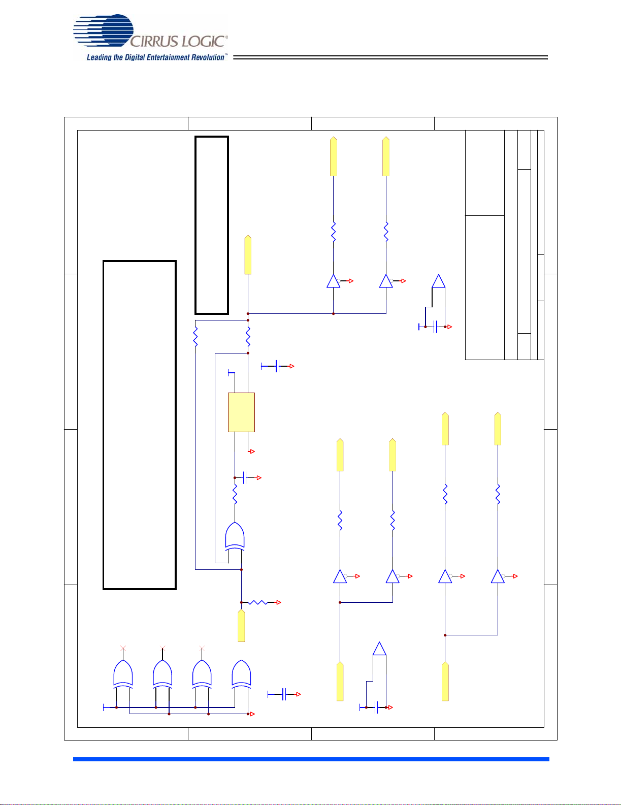
Appendix D: EV-2 Schematic Drawings
4
321
PROGRAM#
INIT_IO#
INIT_IO#
PROGRAM#
AD[0..7]
WR#
CNEV_FPGA
EV2_FPGA.Sch
AD[0..7]
WR#
ALE
ALE
D
A[0..7]
A[0..7]
A[8..15]
A[8..15]
RD#
RD#
HRESET#
HWR#
HWR#
HRESET#
SCI_CLK
SCI_CLK
HCS#
HEN#
HEN#
AUX_POWER[0..3]
RSVD[1..4]
AUX_POWER[0..3]
EN_96K
HCS#
RSVD[1..4]
MUTE#
EN_96K
MUTE#
DA_RESET#
EN_96K#
EN_96K#
DA_RESET#
MCU_P17
MCU_P35MCU_P35
MCU_P17
HPF#
HPF#
AD_DATA1
MCU_P35
AD_DATA1
DA_DATA
DA_DATA
SSI_DOUT[0..3] SSI_DIN[0..3]
ADDR3
SSI_DOUT[0..3] SSI_DIN[0..3]
AES_DIN AES_DOUT
AES_BCLK
AES_DIN AES_DOUT
FS512_CLK
AES_BCLK
AD_RESET#
DA_CS#
ADDR3
DA_CS#
AD_RESET#
FS512_CLK
FS1_OUT
MCU_CLK
FS1_OUT
MCU_CLK
C
DA_CCLKDA_CDOUT
DA_CDOUT DA_CCLK
Auxiliary VXCO
FS512_OUT
FS512_OUTFS512_IN
EV2_VCXO.sch
FS512_IN
SSI_CLK
FS1_OUT
AES_FS1
AES_BCLK
SSI_CLK
AES_FS1
FS1_OUT
AES_BCLK
SSI_CLK_IN
FS1_IN
SSI_CLK_IN
FS1_IN
FS512_CLK
MCLK
MCLK
FS512_CLK
B
AES I/O
EV2_AES.Sch
AES_DIN
RESET#
MRESET#
AES_DOUT
AES_DIN
AES_DOUT
AES_BCLK
AES_WCLK
EN_96K#
AES_FS1
AES_BCLK
EN_96K#
EN_96K
EN_96K
A
E
2500 55th Street
Suite 210
Boulder, CO 80301
Engineer: Bill Lowe
1919-Oct-2004Date: Sheet of
CobraNet (TM) Evaluation Board
Cirrus Logic, Inc.
www.peakaudio.com www.cirrus.com
FS512_OUT
Power
FS512_OUT
EV2_pwr.sch
File: EV2_Main.Sch
Title:
Size: Number: Revision:A
SSI_DOUT0
SSI_DOUT1
SSI_DOUT2
SSI_CLK_IN
FS1_IN
SSI_DOUT0
SSI_DOUT1
SSI_CLK_IN
SSI_DIN0
SSI_DIN1
SSI_DIN0
SSI_DIN1
SSI_DOUT3
SSI_DOUT2
SSI_DOUT3
SSI_DIN2
SSI_DIN3
SSI_DIN2
SSI_DIN3
SCI_CLK
FS512_OUT
SCI_CLK
FS512_OUT
FS512_IN
FS512_IN
AUX_POWER[0..3]
AUX_POWER[0..3]
MCLK
A/D Converter
EV2_AD.sch
MCLK
AD_DATA1
AD_DATA1
SSI_CLK
FS1_OUT
FS1_OUT
HPF#
SSI_CLK
HPF#
EN_96K
AD_RESET#
EN_96K
AD_RESET#
A
UPC and logic
EV2_8051.sch
RD#
RD#
HACK#HREQ#
HREQ# HACK#
WR#
WR#MRESET
MRESET
ALE
ALE
D
AD[0..7]
AD[0..7]
WATCHDOG
A[8..15]
MCU_CLK
A[8..15]
MCU_CLK
WATCHDOG
MUTE#
A[0..7]
MUTE#
A[0..7]
TXD
TXDRXD
RXD
INIT_IO# PROGRAM#
MCU_P35
PROGRAM#
INIT_IO#
MRESET
MRESET#
Common components EV2_com.sch
HEN#
HREQ#
HEN#
HACK# HREQ#
HCS#
HCS#
HACK#
MRESET
MRESET#
HRW
HRESET#
HWR#
HRESET#
A[0..2]
MCU_P17
MCU_P17
D/A Converter
EV2_DA.sch
DA_RESET#
DA_RESET#
DA_CDOUT
DA_CDOUT
DA_DATA
MCLK
DA_DATA
MCLK
SSI_CLK
FS1_OUT
FS1_OUT
SSI_CLK
EN_96K
C
EN_96K
DA_CCLK
DA_CCLK
DA_CS#
DA_CS#
A[0..2]
AD[0..7]
MUTE#
WATCHDOG
WATCHDOG
AD[0..7]
RSVD[1..4] MUTE#
ADDR3
RSVD[1..4]
ADDR3
RXD
TXD RXD
TXD
FS1_IN
B
29 Rev. 2.1
1 2 34
Page 30

CobraNet™ EV-2
D
C
B
A
E
B204
AD0
AD1
AD2
AD3
7QH9
SER10A
11
4
A325A2
QH
8
AD4
19
A6
A5
A4
3
2
1
26
A7
A13
A14
B201
.1S
+5V
C13B12D
E3F4G5H
14
2
11432
AD5
AD6
SKT200
SOCKET40
ALE
RD#
WR#
MCU_P35
4
B200
.1S
+5V
C221
10A20S
321
+5V
MCU_CLK
MCU_CLK
3
OUT
GND
VCC
U210
2
4
B210
.1S
+5V
GND
GND
33MHZ OSC
GND
51.1P1S
U200
+5V
ALE
R202
18
30
XTAL2
RST
9
MRESET
MRESET
PSEN#
29
ALE
XTAL119EA
31
R204
PSEN
MCU_P35
WR#
RD#
17
16
15
RD/P3.7
WR/P3. 6
P0.0(AD0)39P0.1(AD1)38P0.2(AD2)37P0.3(AD3)36P0.4(AD4)35P0.5(AD5)34P0.6(AD6)33P0.7(AD7)
AD0
AD1
AD2
GND
4
SW200
1
10KP1S
PSEN#
HACK#
WATCHDOG
WATCHDOG
HREQ#
HACK#
13
TIMER 0/P3.414TIMER 1/P3.5
AD3
AD4
AD5
= ON
2 3
RXD
TXD
HREQ#
TXD
RXD
A14
A15
11
27
28
RXD/P3.010TXD/P3.1
P2.6(A14)
P2.7(A15)
INTR0/P3.212INTR1/P3.3
P1.01P1.12P1.23P1.34P1.45P1.56P1.67P1.7
32
AD6
AD7
INIT_IO#
PROGRAM#
AD[0..7]
INIT_IO#
PROGRAM#
AD[0..7]
DIPSW1_SPDT
Select programming mode.
A13
26
P2.5(A13)
MUTE#
MUTE#
A12
25
P2.4(A12)
HEX_DATA_IN
1
GND
A11
24
HEX_CLOCK
A8A9A10
22
23
P2.0(A8)21P2.1(A9)
P2.2(A10)
P2.3(A11)
8
MCU_P17
HEX_DATA_OUT
HEX_SHIFT
MCU_P17
R206
10KSIP
A[8..15]
A[8..15]
MCU8051
TP200
+5V
R203
TPS
10KP1S
9
8
7
6
5
4
3
2
U202
10
AD7
D011D112D213D315D416D517D618D7
U204
24A021A123
A0A1A2A3A4A5A6
A[0..7]
A[0..7]
CLK INH
SH/LD1CLK
2
15
2
11432
+5V
A12
6
4
8
A11
GND
74HC165
+5V
1
GND
.1S
A8A9A10
A1410A139A128A117A106A95A84A7
U201
R205
GND
CE20OE22WE
RD#
A15
R201
10KP1S
SH/LD1CLK
15
10KSIP
27
R200
+5V WR#
CLK INH
2
2500 55th Street
Suite 210
Boulder, CO 80301
7C199-12
Engineer: Bill Lowe
2919-Oct-2004Date: Sheet of
10KP1S
CobraNet (TM) Evaluation Board - MPC, SRAM and Hex Switches
Cirrus Logic, Inc.
SER10A
2
3
4
5
6
7
8
9
www.peakaudio.com www.cirrus.com
+5V
TP201
TPG
7QH9
QH
C13B12D
E3F4G5H
14
11
10
2
4
11432
8
File: EV2_8051.Sch
Title:
Size: Number: Revision:A
B202
.1S
GND
GND
74HC165
6
GND
2
4
11432
8
1 2 34
C
SW204
5
D
C
+5V
C
BCH SW3
SW203
BCH SW3
5
B
SW202
C
5
C
BCH SW3
SW201
5
A
Rev. 2.1 30
BCH SW3
Page 31

CobraNet™ EV-2
D
C
B
A
E
MCLK
SSI_CLK
MCLK
SSI_CLK
FS1_OUT
4
3
5
VL
SCLK
MCLK
VD
VA
FILT+24REF_GND
23
C307
.01S8
FS1_OUT
AD_DATA1
AD_DATA1
CR300
VCC_+3
9
LRCK
SDOUT
22
GND
C350
.01S8
C308
10A6S
+
LED0603R
VQ
VQ
R305
R352
90.9P1S
10KP1S
AINR+
21
4
C305
10A6S
+
GND
C353
B352
R361
+5VA
.1S
.01S8
5.11P1S
B351
C352
10A6S
+
U350
8
6
19
.1S
GNDGND
C351
47A16AES
VCC_+3
GND
321
AD_RESET#
AD_RESET#
1
15
12
RST
OVFL
20
C306
2700PFS8
2
M/S
I2S/LJ
AINR-
HPF#
HPF#
11
HPF
EN_96K
EN_96K
13
M114M0
AINL-
17
10
MDIV
C326
2700PFS8
R360
AINL+
16
1KP1S
GND
AGND
AGND
GND
CS5381
2500 55th Street
Suite 210
Boulder, CO 80301
Engineer: Bill Lowe
18
7
GND GND
Cirrus Logic, Inc.
www.peakaudio.com www.cirrus.com
TP300
TPG
GND
3919-Oct-2004Date: Sheet of
CobraNet (TM) Evaluation Board - ADC
Title:
File: EV2_AD.Sch
Size: Number: Revision:A
C301
R303
634P1S
GND
B300
.1S
470PFS8
74
+9VA
D
U300
R313
634P1S
R300
90.9P1S
6
B301
.1S
OPA627
5
1
C311
470PFS8
-9VA
3
2
R302
10KP.1S
C302
.01S8
VQ
R301
GND
100KS
C300
10A20S
R310
6
GND
U310
B310
.1S
74
+9VA
2
R312
10KP.1S
C310
C
90.9P1S
3
10A20S
GND
B311
.1S
OPA627
5
1
J300
C331
-9VA
R311
100KS
6
12345
470PFS8
1X6PHNX
R333
634P1S
R330
6
GND
U330
B330
.1S
74
+9VA
2
C330
10A20S
GND
B
90.9P1S
3
R332
R331
R323
634P1S
R320
90.9P1S
GND
B331
.1S
OPA627
5
1
C321
470PFS8
-9VA
10KP.1S
C332
100KS
R321
100KS
.01S8
GND
+9VA B320
VQ
6
GND
U320
.1S
74
3
2
R322
10KP.1S
C320
A
10A20S
GND
B321
.1S
OPA627
5
1
-9VA
1 2 34
31 Rev. 2.1
Page 32

CobraNet™ EV-2
A
E
2500 55th Street
Suite 210
Boulder, CO 80301
Engineer: Bill Lowe
4919-Oct-2004Date: Sheet of
CobraNet (TM) Evaluation Board - DAC
Cirrus Logic, Inc.
www.peakaudio.com www.cirrus.com
File: EV2_DA.Sch
Title:
Size: Number: Revision:A
R436
100KS
47A16AES
C434
4560
464P1S
0.015UF
C431
B
C444
-9VB
2200PFS
R446
GND
100KS
C442
0.015UF
U430A
C441
2200PFS
GND
47A16AES
R445
196P1S
1
4560
+9VB
8 4
3
2
R442
464P1S
C443
0.018UF
C422
R425
1
3
2200PFS
R422
47A16AES
196P1S
2
464P1S
C
12345
J401
4560
+9VB
8 4
C423
0.018UF
6
1X6PHNX
GND
C432
R435
196P1S
7
U430B
5
6
R432
C433
0.018UF
D
R416
100KS
R426
0.015UF
C411
2200PFS
GND
C424
-9VB
100KS
0.015UF
U410A
C421
GND
4
C412
47A16AES
C414
R415
196P1S
7
U410B
321
4560
5
6
R412
464P1S
C413
0.018UF
+5VB
C401
10A6S
+
B401
.1S
VCC_+3
R411
R410
C400
B400
+
681P1S
196P1S
GND
10A6S
.1S
R407
DA_CS#
EN_96K
TP400
B412
B410
TPG
.1S
.1S
R406
R405
R404
1KP1S
1KP1S
1KP1S
1KP1S
B413
B411
.1S
.1S
GNDGNDGND
GND
GND
1 2 34
-9VB
GND
C403
10A6S
15
FILT+
SDIN
LRCK
3
DA_DATA
FS1_OUT
DA_DATA
100AE6R3S
+
B403
C402
B402
+5VB
17
VREF
DSD_B
DSD_SCLK
DSD_A
1
2
28
.1S
47A16AES
.1S
16
REF_GND
M3 (AD1/CDIN)
9
GND
EN_96K
EN_96K
R431
GND
R430
20
M0 (AD0/CS)
M2 (SCL/CCLK)
M1 (SDA/CDOUT)
12
10
11
DA_CCLK
DA_CDOUT
DA_CS#
DA_CS#
DA_CCLK
DA_CDOUT
681P1S
196P1S
18
AOUTR+
BMUTEC
RST
13
DA_RESET#
DA_RESET#
C430
0.015UF
19
AOUTR-
AGND
DGND
CS4398
C440
R403
R441
681P1S
0.015UF
DA_CCLK
R440
196P1S
21
GND
8
1KP1S
GND
DA_CDOUT
+9VB
R421
C420
25
14
0.015UF
AMUTEC
VLC
R420
24
AOUTL-
681P1S
196P1S
C404
MCLK
6
MCLK
MCLK
GND
+
26
VQ
SCLK
4
5
FS1_OUT
SSI_CLK
SSI_CLK
C410
0.015UF
23
U400
AOUTL+
VA
22
VD
7
VLS
27
B404
.1S
GND
D
C
B
A
Rev. 2.1 32
Page 33

CobraNet™ EV-2
MRESET#
4
MRESET#
+
Reset Circuit
C508
10A6S
VCC_+3
321
SW508
U508E
U508F
SW2349
D
C
B
A
E
MRESET
10
11
12
13
74LVX14S
74LVX14S
CR508
U508C
R508
10KP1S
1N4148S
5
RXD
RXD
12
T1OUT
R1OUT
R1IN
T1IN
13
TXD
P504
DB9FRA
GND
SCI_RXD
7
9
T2OUT
R2OUT
T2IN
R2IN
8
10
SCI_TXD
1
MAX232A
6
2
7
3
8
P501
1
6
2
7
3
8
4
9
6
5
C511
+
8
74LVX14S
U508D
9
U508G
GND
VCC_+3
10A6S
2
U508A
74LVX14S
1
GND
VCC
74LVX14S
7
14
GND
B508
.1S
8051 com
74LVX14S
GND
C503
.1S
C504
+5V
Serial Interface
C502
U507
6
2
VS+
C1+
C1-
1
4
3
.1S
C501
VS-
C2+
GND
.1S
14
C2-
5
11
TXD
.1S
4
9
5
DB9FRA
GND
2500 55th Street
CM com
Suite 210
Boulder, CO 80301
Engineer: Bill Lowe
5919-Oct-2004Date: Sheet of
CobraNet (TM) Evaluation Board - CM & serial I/O, and reset circuit.
Cirrus Logic, Inc.
www.peakaudio.com www.cirrus.com
File: EV2_com.Sch
Title:
Size: Number: Revision:A
C510
10A6S
+
B511
.1S
GND
B510
.1S
VCC_+3
GND
GND
GND
VCC_+3
VCC_+3
VCC_+3
2
4
6
8
10
12
14
P510
1
3
5
7
9
11
13
HREQ#
HACK#
HCS#
SCI_RXD SCI_TXD
SCI_CLK
HRW
HEN#
HRW
HCS#
HEN#
HREQ#
TPS
SCI_CLK
D
HACK#
A[0..2]
A[0..2]
CobraNet Module Connectors
TP500
GND
VCC_+3
16
18
15
17
A0A1A2
GND
20
19
AD[0..7]
AD[0..7]
VCC_+3
22
24
21
23
AD0
AD1
GND
26
25
AD2
GND
VCC_+3
28
30
27
29
AD3
AD4
VCC_+3
32
31
AD5
GND
34
33
AD6
VCC_+3
3
2
1
J500
3SRHDR
RSVD1
GND
VCC_+3
36
38
40
35
37
39
HRESET#
ADDR3
AD7
HRESET#
ADDR3
C
C512
10A6S
VCC_+3
GND
VCC_+3
6
8
5
7
FS512_OUT
FS1_IN
FS1_IN
MUTE#
B513
B512
GND
VCC_+3
VCC_+3
10
12
9
11
FS512_IN
REF_CLK_IN
FS512_IN
FS512_OUT
+
.1S
.1S
GND
GND
VCC_+3
VCC_+3
14
16
18
20
13
15
17
19
SSI_DOUT0
SSI_DOUT1
SSI_DOUT2
SSI_CLK_IN
SSI_DOUT0
SSI_DOUT1
SSI_DOUT2
SSI_CLK_IN
C513
+
GND
B514
+5V
GND
GND
VCC_+3
22
24
26
28
21
23
25
27
SSI_DOUT3
SSI_DIN0
SSI_DIN1
SSI_DIN2
SSI_DIN0
SSI_DIN1
SSI_DOUT3
B
10A6S
.1S
GND
GND
VCC_+3
30
32
34
29
31
33
SSI_DIN3
RSVD3
SSI_DIN2
SSI_DIN3
GND
+5V
+5V
36
38
35
37
RSVD4
AUX_POWER2 AUX_POWER3
WATCHDOG
WATCHDOG
40
39
AUX_POWER0 AUX_POWER1
MMS_CONN40
AUX_POWER[0..3]
1 2 34
TP501
TPG
GND
AUX_POWER[0..3]
A
GND
FS1_IN
REF_CLK_IN
GND
2
4
MMS_CONN40
P511
1
3
RSVD2
MUTE#
RSVD[1..4]
RSVD[1..4]
33 Rev. 2.1
Page 34
CobraNet™ EV-2
D
C
B
A
E
MCLK
4
MCLK
R503
51.1P1S
FS512_OUT
74LVX125A
1
2 3
SSI_CLK
U501A
Clock buffers
Without VCXO populate R501 and not R602.
R501
321
51.1P1S
FS512_EV
FS512_OUT
With VCXO populate R602 and not R501.
R602
51.1P1S
B600
.1S
GND
Optional VCXO
4
VCC_+3
VCC
VC
U600
1
R603
3
3
OUT
GND
2
C606
464P1S
VCC_+3
24.576MHZ VCXO
GND
.1S
GND
GND
U501D
74LVX125A
FS512_CLK
FS512_CLK
R502
51.1P1S
12 11
AES_BCLK
AES_BCLK
13
GND
VCC_+3
U501E
VCC14GND
7
B501
.1S
FS1_OUT
FS1_OUT
R515
74LVX125A
GND
51.1P1S
2500 55th Street
Suite 210
Boulder, CO 80301
Engineer: Bill Lowe
6919-Oct-2004Date: Sheet of
CobraNet (TM) Evaluation Board - Optional VCXO and clock buffers.
Cirrus Logic, Inc.
www.peakaudio.com www.cirrus.com
Title:
File: EV2_VCXO.Sch
Size: Number: Revision:A
AES_FS1
AES_FS1
R514
51.1P1S
R511
The VCXO circuit provides an example of a circuit that will reduce jitter on the
master clock. In the EV-2 application jitter is low enough where this circuit does
not improve the jitter performance significantly. The end user, because of long
trace lengths or running the master clock through other components such as gates
or FPGAs, may want to consider implementing a jitter attenuation circuit such as
6
U601B
74LVX86S
U601C
4
5
9
VCC_+3
D
this one.
8
74LVX86S
10
U601D
12
51.1P1S
U601A
74LVX86S
1
2
U510C
74LVX125A
FS512_IN
R606
10KP1S
FS512_IN
11
VCC14GND
74LVX86S
U601E
74LVX86S
13
7
VCC_+3
GND
C
Clock buffers
GND
B601
.1S
GND
SSI_CLK_IN SSI_CLK9 8
SSI_CLK_IN
VCC_+3
10
GND
U510E
R512
U510B
74LVX125A
5 6
VCC14GND
7
B500
.1S
B
51.1P1S
74LVX125A
GND
74LVX125A
1
GND
2 3
A
74LVX125A
12 11
FS1_IN
FS1_IN
13
GND
U510A
4
GND
U510D
Rev. 2.1 34
1 2 34
Page 35

CobraNet™ EV-2
D
C
B
A
E
12345
J700
GND
C672
23
6
AES_DIN
18
U700
R701
110P1S
R672
249P1S
22PFS
AES_DIN
AES_WCLK
AES_BCLK
17
16
OSCLK
OLRCK
SDOUT
VD+
VA+
RXP4RXN
5
3
L702
1
R673
R708
OMCK
21
AES_MCLK
4
321
B701
.1S
+5V
BD700
FBS1
B700
GNDGND
.1S
90.9P1S
110P1S
26
TXP
6
AES_RXN
AES_RXP
PE65612
2 4
25
11
TXN
RERR
ILRCK
ISCLK
SDIN
12
13
14
AES_DOUT
AES_WCLK
AES_BCLK
1X6PHNX
GND
2500 55th Street
Suite 210
Boulder, CO 80301
CR710
19
EMPH/U
AUDIO/V
9
RESET#
15
TCBL
DGND
AGND
FILT8RST
CS8420
R709
LED0603R
R706
10KP1S
R705
10KP1S
R704
10KP1S
R703
10KP1S
22
7
249P1S
GNDGND
R711
GND
GND
GND GND
GND
1.54KP1S
C700
C701
8200PFS
.47S
GND
U501C
74LVX125A
9 8
FS512_OUT
14
VCC_+3VCC_+3
VCC
Q5Q
Cirrus Logic, Inc.
www.peakaudio.com www.cirrus.com
AES_MCLK
R507
51.1P1S
10
U501B
74LVX125A
5 6
EN_96K#
EN_96K#
GND
6
7
GND
8
Q9Q
R710
464P1S
+5V
R707
10KP1S
3
28
10
20
1
ORIG
COPY
RMCK
PRO/C
DFC0
H/S
DFC1
2
24
27
CobraNet (TM) Evaluation Board - AES Transceiver
Title:
Size: Number: Revision:A
4
EN_96K
EN_96K
Engineer: Bill Lowe
7919-Oct-2004Date: Sheet of
File: EV2_AES.Sch
1
24
L701
PE65612
3
AES_RXP
D
C673
AES_RXN
B672
22PFS
.1S
GND
AES_BCLK
AES_DOUT
AES_WCLK
GND
C
R702
+5V
10KP1S
+5V
R700
RESET#
10KP1S
B
PRE4CLK3D2CLR
U506A
1
FS512_OUT
FS512_OUT
74LVX74S
VCC_+3
PRE10CLK11D12CLR
U506B
B506
.1S
A
74LVX74S
13
GND
35 Rev. 2.1
1 2 34
Page 36

CobraNet™ EV-2
A
E
2500 55th Street
Suite 210
Boulder, CO 80301
Engineer: Bill Lowe
8919-Oct-2004Date: Sheet of
CobraNet (TM) Evaluation Board - Power
Cirrus Logic, Inc.
VR480
10A20S
4
2
R480
ADJ
IN
www.peakaudio.com www.cirrus.com
249P1S
1
OUT
IN3IN6IN
7
Title:
LM337L
-12V
-9VA
File: EV2_pwr.sch
Size: Number: Revision:A
1 2 34
C473
LM317L
10A20S
C472
B471
+5V
R472
1.54KP1S
.01S8
.1S
+9VA+12V
OUT2OUT3OUT6OUT
IN
VR470
1
B
R513
464P1S
R470
249P1S
7
ADJ
4
GND
R483
1.54KP1S
C482
B481
C471
LM317L
.01S8
.1S
CR504
10A20S
C470
B470
C483
10A20S
R482
249P1S
4
ADJ
IN3IN6IN
IN
VR481
2
LEDPCGRN
R471
1.54KP1S
.01S8
.1S
1
OUT
7
GND
GND
R481
LM337L
-12V
1.54KP1S
C480
B480
-9VB
C481
.01S8
.1S
-12V+5V
14
COM
GND
COM15COM16COM
PS_ON#
17
C
+5V
GND
18
-5VDC
+12V
B456
+ C454
TVS453
+ C453
B455
20
+5VDC19+5VDC
ATX_POWER
10
TVS451
.1S
220AE10S
P4SMB6V8A
220AE10S
.1S
GND
P4SMB13A
C451
470AE16S
+
B452
.1S
B451
.1S
+9VB+12V
OUT2OUT3OUT6OUT
IN
VR471
1
GND
GND
R473
249P1S
7
ADJ
4
D
4
B454
.1S
B453
.1S
C452
470AE16S
+
321
TVS452
P4SMB13A
C461
10A6S
VR460
VR461
3
78M05S
1
+12V +5VB
3
78M05S
1
+12V +5VA
OUT
IN
OUT
IN
+
C460
B460
C463
+
C462
B461
GND
.01S8
.1S
10A6S
GND
.01S8
.1S
GND
2
GND
GND
2
GND
GND
GND
VCC_+3
GND
12
11
13
-12VDC
+3.3VDC
+3.3VDC1+3.3VDC2COM3+5VDC4COM5+5VDC6COM7PWR_OK8+5VSB9+12VDC
P450
TVS450
SMAJ5V0A
220AE10S
+ C450
B450
.1S
D
C
B
A
Rev. 2.1 36
Page 37

CobraNet™ EV-2
D
C
B
A
E
B904
VCC_+3
GND
63
64
GND
(D3) I/O
GND
VCC3
12
13
GND
SSI_DOUT0
A13
62
VCC3
I/O
14
MUTE#
MUTE#
AD4
61
I/O
(D4) I/O
I/O
I/O
15
RSVD2
.1S
A7
A14
59
60
I/O
I/O
I/O
I/O
16
17
ADDR3
RSVD1
ADDR3
RSVD[1..4]
GND
AD5
A5
A6
56
57
58
I/O
I/O
(D5) I/O
I/O
I/O
I/O
19
20
18
HCS#
HEN#
HRESET#
HCS#
HEN#
R902
AD6
AD7
WR#
WR#
53
54
55
(D6) I/O
GCK5, I/O
M1
I/O, GCK2
22
21
23
SCI_CLK
SCI_CLK
1KP1S
PROGRAM#
PROGRAM#
51
52
VCC3
(D7) I/O
PROGRAM
GND
M0
VCC3
24
25
GND
GND
VCC_+3
XCS10XL-4VQ100
DONE
GND
I/O, GCK4
I/O
I/O
I/O
I/O
I/O
I/O
I/O
I/O
I/O
GND
VCC3
I/O (INIT)
I/O
I/O
I/O
I/O
I/O
I/O (LDC)
I/O
I/O (HDC)
I/O, GCK3
PWRDWN
VCC_+3
B905
2500 55th Street
Suite 210
Boulder, CO 80301
CobraNet (TM) Evaluation Board - FPGA
Title:
Size: Number: Revision:A
DA_CCLK
VCC_+3
B906
GND
R901
51.1P1S
DA_DATA
DA_DATA
R905
Engineer: Bill Lowe
9919-Oct-2004Date: Sheet of
File: EV2_FPGA.Sch
.1S
464P1S
1 2 34
.1S
GND
ALE
NC
50
49
GND
48
47
NC
46
45
NC
44
43
42
41
40
39
38
GND
37
36
35
34
33
32
31
30
29
28
27
26
B907
.1S
GND
+5V
Cirrus Logic, Inc.
HPF#
DA_CCLK
HWR#
R904
www.peakaudio.com www.cirrus.com
DA_CDOUT
AD_DATA1
DA_RESET#
AD_RESET#
INIT_IO#
EN_96K
DA_CS#
MCU_P17
FS512_CLK
464P1S
ALE
DA_CDOUT
AD_DATA1
DA_RESET#
HPF#
AD_RESET#
INIT_IO#
EN_96K
DA_CS#
NC
NC
NC
HWR#
MCU_P17
FS512_CLK
R903
464P1S
A[0..7]
AD[0..7]
B901
76
77
78
79
80
81
82
83
84
85
86
87
88
89
90
91
92
93
94
95
96
97
98
99
100
A[0..7]
VCC_+3
U901
.1S
GND
B903
AD[0..7]
I/O
I/O
I/O
I/O
I/O
I/O
I/O
I/O
I/O
I/O
I/O
I/O
I/O
I/O
I/O
I/O
I/O
.1S
GND
GND
VCC3
VCC3
GND
GND
WR#
74
75
VCC3
TDO, O
GCK7, I/O
(CS1) I/O
GCK8, I/O
GND
1
2
FS1_OUT
AD0
A2A3A4
MCU_P35
MCU_P35
73
71
72
CCLK
(D0, DIN) I/O
(DOUT) GCK6, I/O
I/O
I/O, TDI
I/O, GCK1
3
4
5
RSVD3
SSI_DIN2
SSI_DIN3
FS1_OUT
AD1
69
70
I/O
I/O
(D1) I/O
I/O, TMS
I/O, TCK
I/O
6
7
SSI_DIN0
SSI_DIN1
SSI_DIN[0..3]
SSI_DOUT[0..3]
AD2
AD3
A12
65
66
67
68
I/O
I/O
(D2) I/O
I/O
I/O
I/O
9
8
10
11
SSI_DOUT1
SSI_DOUT2
SSI_DOUT3
4
321
4
U508B
3
EN_96K EN_96K#
VCC_+3
AUX_POWER[0..3]
AUX_POWER[0..3]
EN_96K#
74LVX14S
A[8..15]
RD#
MCU_CLK
RD#
B902
A[8..15]
.1S
GND
A1
A11
A10
A0
A9
A15
A8
AES_DIN
AES_DOUT
AES_BCLK
AES_BCLK
MCU_CLK
GND
LED0
GND
LED1
LED2
AES_DIN
AES_DOUT
AUX_POWER2
AUX_POWER0
AUX_POWER1
AUX_POWER3
RSVD4
VCC_+3
CR904
LED1
LEDPCRED
A
CR905
LED2
CR903
SSI_DIN[0..3]
SSI_DOUT[0..3]
VCC_+3
D
C
B908
RSVD[1..4]
HRESET#
.1S
GND
B
LEDPCGRN
LED0
37 Rev. 2.1
LEDPCYLW
Page 38

CobraNet™ EV-2
Appendix E: EV-2 Command Line Interface.
The EV-2 supports a simple command line interface (CLI). This interface allows the user to evaluate the CobraNet module (CM) and monitor and control Host Management Interface (HMI) variables. A list and description of commands follow. Please reference the CobraNet Programmer’s
Manual for more information about the HMI variables. Please note that there is a significant difference between the CM-1 and CM-2 HMI variable format, i.e. how the raw data is stored in the
CM’s memory. Refer to the CobraNet Programmer’s Manual regarding the HMI variable formats.
Command line Syntax
The CLI is case insensitive, either upper or lower case in any combination may be used. Parameters enclosed within < > are mandatory with a few exceptions. At least one white space is
required between command and parameters. Leading, lagging and multiple white spaces are
ignored. A “ctrl-C” or “esc” will abort a command. With exceptions where noted, all numeric values are to be entered or will be displayed in hexadecimal format with a leading “0x”.
This command line interface allows the user to write scripts (i.e Python scripts) that monitor and
control HMI variables. Two commands are supported that allow the user to perform these tasks:
Peek <target> [offset]
This command will return the value at the given address location or the value of the HMI variable.
<target> – a valid host address. The format of <target> is a hexadecimal number with a “0x” prefix.
Example: peek 0xAB12C5
<target> – the user may use an HMI variable.
Example: peek sysdescr
In this example the CLI will return the system description in its entirety.
[offset] – optionally used with HMI array variables only. Offset into the HMI array. If not present
on an HMI array variable, the peek will return a value for the first location in the array.
Example: peek txBundle 0x1000
The above example will peek location 0x51100 or transmitter #1.
Example: peek rxSubMap 0x2005
This example will peek location 0x42005 or receiver #2, channel #5.
Rev. 2.1 38
Page 39

CobraNet™ EV-2
Poke <target> <value> [offset]
This command will set the value of the given location in CobraNet memory space to <value>.
<target>– same as peek above.
<value> – a hexadecimal with a “0x” prefix.
Example: poke 0x40104 0x1011
[offset] – optionally used with HMI array variables only. Offset into the HMI array. If not present
on an HMI array variable the poke will poke the <value> into the first location of the array.
Example: poke txBundle 0x111 0x2000
Please note the difference between the “peek <target = address>” and “<target = HMI>” commands. The
“peek <target = address>” command will return the raw value at the specified address location whereas the
“peek “<target = HMI>” command will return a properly formatted value. The difference is significant
between the CM-1 and CM-2 where the variables are not stored in memory in the same format. An example is the rxPriority HMI variable.
On the CM-1:
peek 0x40104 - command
0x101000 - what is returned
peek rxPriority - command
0x1010 - what is returned
On the CM-2:
peek 0x40104 - command
0x1010 - what is returned
peek rxPriority - command
0x1010 - what is returned
This difference here is that the “peek 0x40104” command returns the raw value as it is stored in memory,
the “peek rxPriority” command returns the value as it should be represented. In this example the CM-1
returned a different value than the CM-2 for the “peek 0x40104” command but the same value for the
“peek rxPriority” command; this is because the storage format of the variable in memory is different
between the CM-1 and CM-2. The main memory architecture difference between the CM-1 and CM-2 is
that the CM-1 has a 24-bit wide memory bus whereas the CM-2 has a 32-bit wide memory bus. In the
above example the rxPriority HMI variable is an Integer16 data type. On the CM-1 this type of data uses
the middle and upper byte of the 24-bit memory location to store the data whereas the CM-2 stores the data
in the lower two bytes of the 32-bit wide memory location.
In summary, using the HMI variable name will return data in the proper format. Using the address will
return the raw data at the address location.
This also applies to the Poke command. When using the “poke <target = address> <value>” command you
must pay attention to how the data (i.e. the <value>) is stored on the respective CM. Where supported,
using the “poke <target=HMI> <value> [offset]” command means that the format of <value> is independent of how the data is stored. This allows for writing a command line interface script that works on either
the CM-1 or the CM-2.
39 Rev. 2.1
Page 40

CobraNet™ EV-2
There are a number of commands that control the state of the EV-2 board. Some of these commands should
prove useful to the user when evaluating the CM. These commands are:
Route <input> <output>
<input> is the audio source on the EV-2 board, valid sources are:
ssi0 – ssi port 0 from the CM.
ssi1 – ssi port 1 from the CM.
ssi2 – ssi port 2 from the CM.
ssi3 – ssi port 3 from the CM.
adc1 – digital audio output #1 from the Cirrus Logic ADC
adc2 – this is the same as adc1.
aes – digital audio output from the Cirrus Logic AES I/O IC.
sine – a sinewave generated on the EV-2 board. This makes a useful test tone.
mute – sets the digital audio stream to all zeros.
<output> is the audio sink on the EV-2 board, valid outputs are:
ssi0 – ssi port 0 to the CM.
ssi1 – ssi port 1 to the CM.
ssi2 – ssi port 2 to the CM.
ssi3 – ssi port 3 to the CM.
dac – digital audio input to the Cirrus Logic DAC.
aes – digital audio input from the Cirrus Logic AES I/O IC.
Examples:
Route ssi0 dac
This will route the CM SSI stream #0 to the DAC.
Route sine aes
This will route a sinewave out to the AES output.
Please note that the route command only applies to audio on and from the perspective of the EV-2 board
and not between Cobranet devices.
Led <color> <operation>
This command controls the state of the three LEDs on the EV-2 board. The y may be used for
development and debugging if so desired.
<color> = red, yellow, green, all. ‘all’ will perform the <operation> on all three LEDs.
<operation> =
on: turn led on
off: turn led off
blink+: blink LED, rate is about 2.2Hz
blink-: turn blink mode off
toggle: change the state of the LED.
Note: blink mode is independent of the LED state. When blink mode is turned off the state will be
returned to the state that the LED was in prior to turning the blink mode on. ‘Off’, ‘On’, and ‘T og gle’ have no effect while blink mode is on but will execute while in blink mode, i.e. when blink
mode is turned off the LED will assume the state of the last command.
Rev. 2.1 40
Page 41

CobraNet™ EV-2
Example: led green toggle.
This will change the state of the green LED. If it was on it will be off. If the LED was in
blink mode the LED will continue to blink but will assume the opposite state prior to the
toggle command if blinking is stopped.
Query <what>
This is a command to return information about the EV-2 and/or CM.
<what> =
system: returns information such as MAC address and software/firmware revision levels.
hex: returns the value of the hex switches on the EV-2 board.
status: Returns the status of the device. Generally the EV-2 and CM will be in one of two
states: Ready or Calibrating. The latter indicates that the EV-2 has the ADC and DAC in
calibration mode. This latter mode occurs only after power up and lasts for about 10 seconds.
cnmute: This returns the state of the mute signal coming from the CM. This is not to be
confused with the mute choice of the route command. This is a signal on the CM interface
that the CM controls. It is in either a muted or unmuted state. Querying this will return the
state.
mac: The CM Ethernet MAC address is returned.
device: This will return the module type, CM-1 or CM-2.
hack: Returns the state of the CM HACK# signal, either a “0” or a “1”.
hreq: Returns the state of the CM HREQ# signal, either a “0” or a “1”.
mute: Returns a list of the outputs paths which are muted .
route: Returns a list of the input to output routing information.
gain: This parameter returns the gain information for the EV-2 sinewave.
frequency: Returns a number from 0x1 to 0x8. See Audio frequency below.
Audio <operation> [value]
<operation> =
samplerate
[value] = 48k: changes the CM samplerate to 48k.
calibrate: put the audio converters through a calibration cycle
[value] = N/A
gain: sets the gain for the EV-2 test sinewave.
[value] = 0dB, -6dB, -12dB, -18dB Default is 0dB.
frequency: sets the frequency for the EV-2 test sinewave.
[value] = 0x1-0x8 This value is a multiple of the fundamental frequency which is
1.5kHz for the 48kHz sample rate and 3.0 kHz for the 96kHz sample rate. Default
is the fundamental.
hpf: enables (0) or disables (1) the high pass filter in the ADC, see the Cirrus Logic
CS5381 data sheet for more details on the operation of the high pass filter.
96k: changes the CM samplerate to 96k.
41 Rev. 2.1
Page 42

TestEV <what>
This is used for manufacturing tests of the EV-2 and in general only the ‘resetcn’ will be useful to
the user.
<what> =
memory – performs an EV-2 memory test, returns either a pass or fail.
watchdog – checks the CM watchdog signal to make sure it is in tolerance. Returns pass
or fail and measured frequency of CM watchdog signal
host – performs a host test, returns pass or fail.
resetcn – resets the CM.
Packet <what> <arg2>
This command will perform a packet transfer between CM/EV-2 boards and is used to demonstrate
and test the Cobranet packet bridge feature. Two packet types are supported, either command
based or text based. The command packet will send an EV-2 line command to the other EV-2
which will return any results (an example would be a query command) as a text based packet. A
text based packet will send text to the other EV-2 to be put out its 8051 serial port. This is much
like an instant message.
<what> =
command: This tells the receiving CM that the following <arg2> is a line command.
text: this tells the receiving CM that the following <arg2> is text and will output the text
to the serial port.
on: turns packet processing on.
off: turns packet processing off.
CobraNet™ EV-2
<arg2>: this is any valid line command as described in this document.
<arg2>: text that may be separated by spaces. Everything that follows the “text”
parameter will be considered text.
Examples:
packet command query device
This example will return what type of CN module is on the other EV-2.
packet text how are you today?
This will send out the 8051 serial port of the other EV-2 the text: how are you
today?
Please note that the on and off commands are from the perspective of the EV-2 and not the CM, i.e., the
CM will still process commands from other sources if set up to do so.
Rev. 2.1 42
Page 43

CobraNet™ EV-2
Read <register>
This command reads the raw value of the host register. Note that the architecture is significantly
different between the CM-1 and CM-2.
<register> =
(for CM-1, the DSP5303 host register interface.)
(for CM-2, the CS1810xx host register interface)
icr: read the icr register.
cvr: read the cvr register.
isr: read the isr register.
ivr: read the ivr register.
drh: read the drh (rxh) register
drm: read the drm (rxm) register
drl: read the drl (rxl) register.
msg: read the msg register (returns four bytes)
data: reads the data register (returns four bytes)
msga: returns the value of the message A register.
msgb: returns the value of the message B register.
msgc: returns the value of the message C register.
msgd: returns the value of the message D register.
dataa: returns the value of the data A register.
datab: returns the value of the data B register.
datac: returns the value of the data C register.
datad: returns the value of the data D register.
control: returns the value of the control register.
status: returns the value of the status register.
Write <register> <value>
This command writes a value to the host register. Refer to the appropriate documentation regarding the host register interface on the CM-1 and CM-2. The architecture is significantly different.
<register> =
(for CM-1, the DSP5303 host register interface.)
icr: write the icr register.
cvr: write the cvr register.
isr: write the isr register.
ivr: write the ivr register.
drh: write the drh (rxh) register
drm: write the drm (rxm) register
drl: write the drl (rxl) register.
(for CM-2, the CS1810xx host register interface)
msg: write the msg register (writes four bytes)
data: write the data register (writes four bytes)
msga: write the value to the message A register.
msgb: write the value to the message B register.
msgc: write the value to the message C register.
msgd: write the value to the message D register.
dataa: write the value to the data A register.
43 Rev. 2.1
Page 44

datab: write the value to the data B register.
datac: write the value to the data C register.
datad: write the value to the data D register.
<value> – a hexadecimal with a “0x” prefix. The individual registers are byte wide, a hexadecimal in the <value>
parameter greater than a byte will only use the least significant byte.
Example: write msgc 0xb3
Please note that writing certain registers may trigger CobraNet events. Please refer to the CobraNet Programmer’s Manual for
more information regarding these registers and the other host interface registers.
Peekev <target>
This command will return the value at the given address location for the EV-2 data memory. Please refer to the earlier
discussion of the EV-2 memory map.
<target> = a valid address in hex format. The address is limited to two bytes.
Pokeev <target> <value>
This command will set the given address location in the EV-2 data memory to the given <value>. Please refer to the
earlier discussion of the EV-2 memory map.
<target> – a valid address in hex format. The address is limited to two bytes.
<value> – a byte hexadecimal with a “0x” prefix.
Contacting Cirrus Logic, Inc.
For further information on CobraNet™ products, contact: the Commercial Audio Products Division of Cirrus Logic, Inc.
2500 55th St. Suite 210 Boulder, CO 80301 (303) 245-5500
sales@peakaudio.com
www.cirrus.com
Copyright © 2001-05 Cirrus Logic, Inc. All rights reserved. CobraNet and Peak Audio are trademarks of Cirrus Logic, Inc.
 Loading...