

Page 1

EP93XX
ARM®9 Embedded Processor Family
EP93xx
User’s Guide
http://www.cirrus.com
©Copyright 2007 Cirrus Logic, Inc. SEP 2007
DS785UM1
Page 2

EP93xx User’s Guide
Contacting Cirrus Logic Support
For all product questions and inquiries contact a Cirrus Logic Sales Representative.
To find the one nearest to you go to www.cirrus.com
Cirrus Logic, Inc. and its sub si di ari es ( “Ci rrus”) believe that the inform at ion contained in this document i s accurate and reliable. However, the information
is subject to change without not ice and is provi ded “AS IS” wi thout warranty of an y kind (exp ress or implied). Customer s are advised to obtain the latest
version of relevant information to verify, before placing orders, that information being relied on is current and complete. All products are sold subject to the
terms and conditions of sale supplied at th e time of order acknowledg ment, includ ing those pert aining to warrant y, patent inf ringement, and limitation of
liability. No respons ibility is assumed by Cirrus f or the use of this information, including use of this information as the basis for manufacture or sale of any
items, or for infringement of patents or other rights of third parties. This document is the property of Cirrus and by furnishing this information, Cirrus grants
no license, express or implied under any patents, mask work rights, copyrights, trademarks, trade secrets or other intellectual property rights. Cirrus owns
the copyrights associated with the information contained herein and gives consent for copies to be made of the information only f o r use wi thi n your organization with respect to Cirrus integr ated circuits or ot her products of Cir rus. This consent does not extend to other copy ing such as copying for ge neral
distribution, advertising or promotional purposes, or for creating any work for resale.
CERTAIN APPLICATIONS USING SEMICO NDUCTOR PRODUCTS MAY INVOLVE POTENTIAL RISKS OF DEATH, PERSONAL INJURY, OR SEVERE
PROPERTY OR ENVIRONMENTAL DAMAGE (“CRITICAL APPLICATIONS”). CIRRUS PRODUCTS ARE NOT DESIGNED, AUTHORIZED OR WARRANTED FOR USE IN AIRCRAFT SYSTEMS, MILITARY APP LICATIONS , PRODUCTS SURGICALLY IMP LANTE D INTO THE BODY, LIFE SUP PORT
PRODUCTS OR OTHER CRITICAL APPLICATIONS (INCLUDING MEDICAL DEVICES, AIRCRAFT SYSTEMS OR COMPONENTS AND PERSONAL
OR AUTOMOTIVE SAFETY OR SECURITY DEVICE S). INCLUSION OF CIRRUS PRODUCTS IN SUCH APPLICATIONS IS UNDERSTOOD T O BE FULLY AT THE CUSTOMER'S RISK AND CIRRUS DISCLAIMS AND MAKES NO WARRANTY, EXPRESS, STATUTORY OR IMPLIED, INCLUDING THE
IMPLIED WARRANTIES OF MERCHANTABILITY AND FITNESS FOR PARTICULAR PURPOSE, WITH REGARD TO ANY CIRRUS PRODUCT THAT
IS USED IN SUCH A MANNER. IF THE CUSTOMER OR CUSTOM ER'S CUSTOMER USES OR PE RMITS THE USE OF CIRRU S PRODUCTS IN CRITICAL APPLICATIONS, CUSTOMER AGREES, BY SUCH USE , TO FULLY INDEMNIFY CIRRUS, ITS OFFICERS, DIRECTORS, EMPLOYE ES, DISTRIBUTORS AND OTHER AGENTS F ROM ANY AND A LL LIABILITY, INCLUDING ATTORNEYS ' FEES AND COS TS, THAT MAY RESU LT FROM OR ARISE
IN CONNECTION WITH THESE USES.
Cirrus Logic, Cirrus, MaverickCrunch, MaverickKey, and the Cirrus Log ic logo designs are tradema rks of Cirrus Logic, Inc. Al l other brand and pr oduct
names in this document may be trademarks or service marks of their respective owners.
Microsoft, Windows, and Windows CE are registered trademarks of Microsoft Corporation.
Microwire is a trademark of National Semiconductor Corp. National Semiconductor is a registered trademark of National Semiconductor Corp.
Texas Instruments is a registered trademark of Texas Instruments, Inc.
Motorola is a registered trademark of Motorola, Inc.
LINUX is a registered trademark of Linus Torvalds.
ARM and Thumb are registered trademarks of ARM Limited
Intel is a registered trademark of Intel Corporation
Hewlett-Packard is a registered trademark of Hewlett-Packard Corporation.
Compaq is a regis t e red trademark of BV, a private Limited Liability Company in the Netherlands.
DS785UM1 ©Copyright 2007 Cirrus Logic, Inc. ii
Page 3

EP93xx User’s Guide
Contents
Chapter Figures. . . . . . . . . . . . . . . . . . . . . . . . . . . . . . . . . . . . . . . . . . . . . . . . . . . . . . . . . . . . . . . . .xiv
Chapter Tables . . . . . . . . . . . . . . . . . . . . . . . . . . . . . . . . . . . . . . . . . . . . . . . . . . . . . . . . . . . . . . . . xvii
Revision History . . . . . . . . . . . . . . . . . . . . . . . . . . . . . . . . . . . . . . . . . . . . . . . . . . . . . . . . . . . . . . . xxii
Preface................................................................................................................... P-1
P.1 About the EP93xx User’s Guide. . . . . . . . . . . . . . . . . . . . . . . . . . . . . . . . . . . . . . . . . . . . . . . P-1
P.2 Related Documents from Cirrus Logic . . . . . . . . . . . . . . . . . . . . . . . . . . . . . . . . . . . . . . . . . P-3
P.3 Reference Documents. . . . . . . . . . . . . . . . . . . . . . . . . . . . . . . . . . . . . . . . . . . . . . . . . . . . . . . P-3
P.4 Notational Conventions . . . . . . . . . . . . . . . . . . . . . . . . . . . . . . . . . . . . . . . . . . . . . . . . . . . . . P-3
P.5 Register Example. . . . . . . . . . . . . . . . . . . . . . . . . . . . . . . . . . . . . . . . . . . . . . . . . . . . . . . . . . . P-4
Chapter 1. Introduction.........................................................................................1-1
1.1 Introduction . . . . . . . . . . . . . . . . . . . . . . . . . . . . . . . . . . . . . . . . . . . . . . . . . . . . . . . . . . . . . . . .1-1
1.2 EP93xx Features . . . . . . . . . . . . . . . . . . . . . . . . . . . . . . . . . . . . . . . . . . . . . . . . . . . . . . . . . . . .1-1
1.3 EP93xx Processor Applications. . . . . . . . . . . . . . . . . . . . . . . . . . . . . . . . . . . . . . . . . . . . . . . .1-7
1.4 EP93xx Processor Highlights. . . . . . . . . . . . . . . . . . . . . . . . . . . . . . . . . . . . . . . . . . . . . . . . . .1-7
1.4.1 High-Performance ARM920T Core .................................................................................1-7
1.4.2 MaverickCrunch
1.4.3 MaverickKey
1.4.4 Integrated Multi-Port USB 2.0 Full Speed Hosts with Transceivers ................................1-8
1.4.5 Integrated Ethernet MAC Reduces BOM Costs ........................................ ...... ....... .........1-9
1.4.6 8x8 Keypad Interface Reduces BOM Costs....................................................................1-9
1.4.7 Multiple Booting Mechanisms Increase Flexibility...........................................................1-9
1.4.8 Abundant General Purpose I/Os Build Flexible Systems ................................................1-9
1.4.9 General-Purpose Memory Interface (SDRAM, SRAM, ROM, FLASH) ...........................1-9
1.4.10 12-Bit Analog-to-Digital Converter (ADC) Provides an Integrated
Touch-Screen Interface or General ADC Functionality..........................................................1-10
1.4.11 Raster Analog / LCD Controller...................................................................................1-10
1.4.12 Graphics Accelerator...................................................................................................1-10
1.4.13 PCMCIA Interface........................................................................................................1-10
™
Co-processor for Ultra-Fast Math Processing....................................1-7
™
Unique ID Secures Digital Content in OEM Designs ..............................1-8
Chapter 2. ARM920T Core and Advanced High-Speed Bus (AHB)...................2-1
2.1 Introduction . . . . . . . . . . . . . . . . . . . . . . . . . . . . . . . . . . . . . . . . . . . . . . . . . . . . . . . . . . . . . . . .2-1
2.2 Overview: ARM920T Core . . . . . . . . . . . . . . . . . . . . . . . . . . . . . . . . . . . . . . . . . . . . . . . . . . . . .2-1
2.2.1 Features ..........................................................................................................................2-1
2.2.2 Block Diagram .................................................................................................................2-2
2.2.3 Operations.......................................................................................................................2-2
2.2.3.1 ARM9TDMI Core ...........................................................................................2-3
2.2.3.2 Memory Management Unit ............................................................................2-4
2.2.3.3 Cache and Write Buffer .................................................................................2-5
2.2.4 Co-processor Interface....................................................................................................2-6
2.2.5 AMBA AHB Bus Interface Overview................................................................................2-6
2.2.6 AHB Implementation Details............................................................................................2-7
2.2.7 Memory and Bus Access Errors......................................................................................2-9
2.2.8 Bus Arbitration.................................................................................................................2-9
2.2.8.1 Main AHB Bus Arbiter..................................................................................2-10
2.2.8.2 SDRAM Slave Arbiter..................................................................................2-11
2.2.8.3 EBI Bus Arbiter............................................................................................2-11
2.3 AHB Decoder . . . . . . . . . . . . . . . . . . . . . . . . . . . . . . . . . . . . . . . . . . . . . . . . . . . . . . . . . . . . . .2-11
2.3.1 AHB Slave .....................................................................................................................2-11
DS785UM1 ©Copyright 2007 Cirrus Logic, Inc. iii
Page 4

EP93xx User’s Guide
2.3.2 AHB-to-APB Bridge.......................................................................................................2-12
2.3.2.1 Function and Operation of the AHB-to-APB Bridge.....................................2-12
2.3.3 APB Slave .....................................................................................................................2-13
2.3.4 Register Definitions .......................................................................................................2-13
2.3.5 Memory Map..................................................................................................................2-16
2.3.6 Internal Register Map ....................................................................................................2-17
2.3.6.1 Memory Access Rules.................................................................................2-17
Chapter 3. MaverickCrunch Co-Processor .........................................................3-1
3.1 Introduction . . . . . . . . . . . . . . . . . . . . . . . . . . . . . . . . . . . . . . . . . . . . . . . . . . . . . . . . . . . . . . . .3-1
3.1.1 Features ..........................................................................................................................3-1
3.1.2 Operational Overview......................................................................................................3-1
3.1.3 Pipelines and Latency .....................................................................................................3-3
3.1.4 Data Registers.................................................................................................................3-3
3.1.5 Integer Saturation Arithmetic...........................................................................................3-4
3.1.6 Comparisons ...................................................................................................................3-6
3.2 Programming Examples . . . . . . . . . . . . . . . . . . . . . . . . . . . . . . . . . . . . . . . . . . . . . . . . . . . . . .3-8
3.2.1 Example 1........................................................................................................................3-8
3.2.1.1 Setup Code....................................................................................................3-8
3.2.1.2 C Code...........................................................................................................3-8
3.2.1.3 Accessing MaverickCrunch with ARM Co-Processor Instructions.................3-8
3.2.1.4 MaverickCrunch Assembly Language Instructions........................................3-8
3.2.2 Example 2........................................................................................................................3-9
3.2.2.1 C Code...........................................................................................................3-9
3.2.2.2 MaverickCrunch Assembly Language Instructions........................................3-9
3.3 DSPSC Register . . . . . . . . . . . . . . . . . . . . . . . . . . . . . . . . . . . . . . . . . . . . . . . . . . . . . . . . . . . .3-10
3.4 ARM Co-Processor Instruction Format . . . . . . . . . . . . . . . . . . . . . . . . . . . . . . . . . . . . . . . . .3-14
3.5 Instruction Set for the MaverickCrunch Co-Processor . . . . . . . . . . . . . . . . . . . . . . . . . . . .3-17
3.5.1 Load and Store Instructions...........................................................................................3-21
3.5.2 Move Instructions ..........................................................................................................3-24
3.5.3 Accumulator and DSPSC Move Instructions.................................................................3-27
3.5.4 Copy and Conversion Instructions.................................................................................3-31
3.5.5 Shift Instructions............................................................................................................3-35
3.5.6 Compare Instructions ....................................................................................................3-36
3.5.7 Floating Point Arithmetic Instructions ............................................................................3-38
3.5.8 Integer Arithmetic Instructions.......................................................................................3-41
3.5.9 Accumulator Arithmetic Instructions ..............................................................................3-45
Chapter 4. Boot ROM ............................................................................................4-1
4.1 Introduction . . . . . . . . . . . . . . . . . . . . . . . . . . . . . . . . . . . . . . . . . . . . . . . . . . . . . . . . . . . . . . . .4-1
4.1.1 Boot ROM Hardware Operational Overview....................................................................4-1
4.1.1.1 Memory Map..................................................................................................4-1
4.1.2 Boot ROM Software Operational Overview.....................................................................4-1
4.1.2.1 Image Header................................................................................................4-2
4.1.2.2 Boot Algorithm ...............................................................................................4-2
4.1.2.3 Flowchart .......................................................................................................4-3
4.2 Boot Options . . . . . . . . . . . . . . . . . . . . . . . . . . . . . . . . . . . . . . . . . . . . . . . . . . . . . . . . . . . . . . .4-4
4.2.1 UART Boot ......................................................................................................................4-6
4.2.2 SPI Boot ..........................................................................................................................4-6
4.2.3 FLASH Boot.....................................................................................................................4-6
4.2.4 SDRAM or SyncFLASH Boot ..........................................................................................4-7
iv ©Copyright 2007 Cirrus Logic, Inc. DS785UM1
Page 5

EP93xx User’s Guide
4.2.5 Synchronous Memory Operation............................................................... ...... ....... ...... ...4-7
Chapter 5. System Controller...............................................................................5-1
5.1 Introduction . . . . . . . . . . . . . . . . . . . . . . . . . . . . . . . . . . . . . . . . . . . . . . . . . . . . . . . . . . . . . . . .5-1
5.1.1 System Startup................................................................................................................5-1
5.1.2 System Reset ..................................................................................................................5-1
5.1.3 Hardware Configuration Control......................................................................................5-2
5.1.4 Software System Configuration Options..........................................................................5-4
5.1.5 Clock Control...................................................................................................................5-4
5.1.5.1 Oscillators and Programmable PLLs .............................................................5-4
5.1.5.2 Bus and Peripheral Clock Generation ...........................................................5-5
5.1.5.3 Steps for Clock Configuration........................................................................5-9
5.1.6 Power Management ........................................................................................................5-9
5.1.6.1 Clock Gatings ................................................................................................5-9
5.1.6.2 System Power States ..................................................................................5-10
5.1.7 Interrupt Generation ......................................................................................................5-12
5.2 Registers. . . . . . . . . . . . . . . . . . . . . . . . . . . . . . . . . . . . . . . . . . . . . . . . . . . . . . . . . . . . . . . . . .5-13
Chapter 6. Vectored Interrupt Controller.............................................................6-1
6.1 Introduction . . . . . . . . . . . . . . . . . . . . . . . . . . . . . . . . . . . . . . . . . . . . . . . . . . . . . . . . . . . . . . . .6-1
6.1.1 Interrupt Priority...............................................................................................................6-2
6.1.2 Interrupt Configuration.....................................................................................................6-3
6.1.3 Interrupt Details ...............................................................................................................6-4
6.2 Registers. . . . . . . . . . . . . . . . . . . . . . . . . . . . . . . . . . . . . . . . . . . . . . . . . . . . . . . . . . . . . . . . . . .6-8
Chapter 7. Raster Engine With Analog/LCD Integrated
Timing and Interface ............................................................................................7-1
7.1 Introduction . . . . . . . . . . . . . . . . . . . . . . . . . . . . . . . . . . . . . . . . . . . . . . . . . . . . . . . . . . . . . . . .7-1
7.2 Features . . . . . . . . . . . . . . . . . . . . . . . . . . . . . . . . . . . . . . . . . . . . . . . . . . . . . . . . . . . . . . . . . . .7-3
7.3 Raster Engine Features Overview . . . . . . . . . . . . . . . . . . . . . . . . . . . . . . . . . . . . . . . . . . . . . .7-3
7.3.1 Hardware Blinking ...........................................................................................................7-3
7.3.2 Color Look-Up Tables......................................................................................................7-4
7.3.3 Grayscale/Color Generation for Monochrome/Passive Low Color Displays ...................7-4
7.3.4 Frame Buffer Organization..............................................................................................7-4
7.3.5 Frame Buffer Memory Size..............................................................................................7-6
7.3.6 Pulse Width Modulated Brightness..................................................................................7-6
7.3.7 Hardware Cursor .............................................................................................................7-7
7.4 Functional Details . . . . . . . . . . . . . . . . . . . . . . . . . . . . . . . . . . . . . . . . . . . . . . . . . . . . . . . . . . .7-7
7.4.1 VILOSATI (Video Image Line Output Scanner and Transfer Interface) ..........................7-8
7.4.2 Video FIFO ......................................................................................................................7-9
7.4.3 Video Pixel MUX............................................................................................................7-10
7.4.4 Blink Function................................................................................................................7-10
7.4.5 Color Look-Up-Tables ...................................................................................................7-11
7.4.6 Color RGB Mux .............................................................................................................7-11
7.4.7 Pixel Shift Logic.............................................................................................................7-12
7.4.8 Grayscale/Color Generator for Monochrome/Passive Low Color Displays ...................7-15
7.4.8.1 HORZ_CNT3, HORZ_CNT4 Counters........................................................7-16
7.4.8.2 VERT_CNT3, VERT_CNT4 Counters .........................................................7-16
7.4.8.3 FRAME_CNT3, FRAME_CNT4 Counters ...................................................7-16
7.4.8.4 HORZ_CNTx (pixel) timing..........................................................................7-16
7.4.8.5 VERT_CNTx (line) timing ............................................................................7-16
DS785UM1 ©Copyright 2007 Cirrus Logic, Inc. v
Page 6

EP93xx User’s Guide
7.4.8.6 FRAME_CNTx timing ..................................................................................7-16
7.4.8.7 Grayscale Look-Up Table (GrySclLUT).......................................................7-17
7.4.8.8 GrySclLUT Timing Diagram.........................................................................7-18
7.4.9 Hardware Cursor ...........................................................................................................7-24
7.4.9.1 Registers Used for Cursor ...........................................................................7-26
7.4.10 Video Timing................................................................................................................7-28
7.4.10.1 Setting the Video Memory Parameters......................................................7-31
7.4.10.2 PixelMode ..................................................................................................7-32
7.4.11 Blink Logic ...................................................................................................................7-32
7.4.11.1 BlinkRate ...................................................................................................7-32
7.4.11.2 Defining Blink Pixels ..................................................................................7-32
7.4.11.3 Types of Blinking .................................. ....... ...... ....... .................................7-33
7.4.12 Color Mode Definition..................................................................................................7-35
7.4.12.1 Pixel Look-up Table Mode.........................................................................7-35
7.4.12.2 Triple 8-bit Color Definition Mode ..............................................................7-35
7.4.12.3 16-bit 565 Color Definition Mode ...............................................................7-35
7.4.12.4 16-bit 555 Color Definition Mode ...............................................................7-35
7.5 Registers. . . . . . . . . . . . . . . . . . . . . . . . . . . . . . . . . . . . . . . . . . . . . . . . . . . . . . . . . . . . . . . . . .7-36
Chapter 8. Graphics Accelerator..........................................................................8-1
8.1 Overview . . . . . . . . . . . . . . . . . . . . . . . . . . . . . . . . . . . . . . . . . . . . . . . . . . . . . . . . . . . . . . . . . . .8-1
8.2 Block Processing Modes. . . . . . . . . . . . . . . . . . . . . . . . . . . . . . . . . . . . . . . . . . . . . . . . . . . . . .8-1
8.2.1 Copy ................................................................................................................................8-2
8.2.1.1 Transparency.................................................................................................8-2
8.2.1.2 Logical Mask..................................................................................................8-2
8.2.1.3 Logical Destination ........................................................................................8-2
8.2.1.4 Operation Precedence...................................................................................8-2
8.2.2 Remapping ......................................................................................................................8-3
8.2.3 Block Fills ........................................................................................................................8-3
8.2.4 Packed Memory Transfer................................................................................................8-3
8.3 Line Draws . . . . . . . . . . . . . . . . . . . . . . . . . . . . . . . . . . . . . . . . . . . . . . . . . . . . . . . . . . . . . . . . .8-3
8.3.1 Breshenham Line Draws.................................................................................................8-4
8.3.2 Pixel Step Line Draws .....................................................................................................8-4
8.4 Memory Organization for Graphics Accelerator . . . . . . . . . . . . . . . . . . . . . . . . . . . . . . . . . . .8-4
8.4.1 Memory Organization for 1 Bit Per Pixel (bpp)...............................................................8-5
8.4.2 Memory Organization for 4-Bits Per Pixel .......................................................................8-5
8.4.3 Memory Organization for 8-Bits Per Pixel .......................................................................8-5
8.4.4 Memory Organization for 16-Bits Per Pixel .....................................................................8-6
8.4.5 Memory Organization for 24-Bits Per Pixel .....................................................................8-7
8.4.6 Memory Map Access.......................................................................................................8-8
8.5 Register Programming . . . . . . . . . . . . . . . . . . . . . . . . . . . . . . . . . . . . . . . . . . . . . . . . . . . . . . .8-8
8.5.1 Word Count .....................................................................................................................8-8
8.5.1.1 Example: 8 BPP mode...................................................................................8-8
8.5.1.2 Example: 24 BPP (packed) mode..................................................................8-9
8.5.2 Pixel End and Start..........................................................................................................8-9
8.5.2.1 4 BPP Word Layout .....................................................................................8-10
8.5.2.2 8 BPP Word Layout .....................................................................................8-11
8.5.2.3 16 BPP WORD Layout ................................................................................8-11
8.5.2.4 24 BPP mode...............................................................................................8-12
8.6 Register Usage. . . . . . . . . . . . . . . . . . . . . . . . . . . . . . . . . . . . . . . . . . . . . . . . . . . . . . . . . . . . .8-13
8.6.1 Breshenham’s Algorithm Line Draw ..............................................................................8-13
8.6.2 Example of Breshenham’s Algori thm Lin e Draw ...... ....... ...... ....... ...... ....... ...... ..............8-1 5
8.6.3 Block Fill Function .........................................................................................................8-16
vi ©Copyright 2007 Cirrus Logic, Inc. DS785UM1
Page 7

EP93xx User’s Guide
8.6.4 Block Copy Function......................................................................................................8-18
8.6.4.1 Example of Block Copy................................................................................8-21
8.7 Registers . . . . . . . . . . . . . . . . . . . . . . . . . . . . . . . . . . . . . . . . . . . . . . . . . . . . . . . . . . . . . . . . .8-22
Chapter 9. 1/10/100 Mbps Ethernet LAN Controller ...........................................9-1
9.1 Introduction . . . . . . . . . . . . . . . . . . . . . . . . . . . . . . . . . . . . . . . . . . . . . . . . . . . . . . . . . . . . . . . .9-1
9.1.1 Detailed Description ........................................................................................................9-1
9.1.1.1 Host Interface and Descriptor Processor.......................................................9-1
9.1.1.2 Reset and Initialization...................................................................................9-2
9.1.1.3 Power-down Modes.......................................................................................9-2
9.1.1.4 Address Space ..............................................................................................9-2
9.1.2 MAC Engine ....................................................................................................................9-3
9.1.2.1 Data Encapsulation........................................................................................9-3
9.1.3 Packet Transmission Process.........................................................................................9-5
9.1.3.1 Carrier Deference..........................................................................................9-5
9.1.4 Transmit Back-Off............................................................................................................9-7
9.1.4.1 Transmission .................................................................................................9-7
9.1.4.2 The FCS Field................................................................................................9-7
9.1.4.3 Bit Order ........................................................................................................9-8
9.1.4.4 Destination Address (DA) Filter .....................................................................9-8
9.1.4.5 Perfect Address Filtering ...............................................................................9-8
9.1.4.6 Hash Filter .....................................................................................................9-9
9.1.4.7 Flow Control.................................................................................................9-10
9.1.4.8 Receive Flow Control...................................................................................9-10
9.1.4.9 Transmit Flow Control..................................................................................9-10
9.1.4.10 Rx Missed and Tx Collision Counters....................................................... .9-11
9.1.4.11 Accessing the MII ......................................................................................9-11
9.2 Descriptor Processor. . . . . . . . . . . . . . . . . . . . . . . . . . . . . . . . . . . . . . . . . . . . . . . . . . . . . . . .9-13
9.2.1 Receive Descriptor Processor Queues .........................................................................9-13
9.2.2 Receive Descriptor Queue ............................................................................................9-13
9.2.3 Receive Status Queue...................................................................................................9-16
9.2.3.1 Receive Status Format................................................................................9-18
9.2.3.2 Receive Flow ...............................................................................................9-21
9.2.3.3 Receive Errors.............................................................................................9-22
9.2.3.4 Receive Descriptor Data/Status Flow..........................................................9-23
9.2.3.5 Receive Descriptor Example .......................................................................9-24
9.2.3.6 Receive Frame Pre-Processing...................................................................9-25
9.2.3.7 Transmit Descriptor Processor Queues.......................................................9-26
9.2.3.8 Transmit Descriptor Queue..........................................................................9-26
9.2.3.9 Transmit Descriptor Format.........................................................................9-28
9.2.3.10 Transmit Status Queue..............................................................................9-30
9.2.3.11 Transmit Status Format .............................................................................9-32
9.2.3.12 Transmit Flow ............................................................................................9-34
9.2.3.13 Transmit Errors..........................................................................................9-35
9.2.3.14 Transmit Descriptor Data/Status Flow.......................................................9-36
9.2.4 Interrupts .......................................................................................................................9-37
9.2.4.1 Interrupt Processing.....................................................................................9-37
9.2.5 Initialization....................................................................................................................9-37
9.2.5.1 Interrupt Processing.....................................................................................9-38
9.2.5.2 Receive Queue Processing .........................................................................9-38
9.2.5.3 Transmit Queue Processing ........................................................................9-38
9.2.5.4 Other Processing.........................................................................................9-38
9.2.5.5 Transmit Restart Process ............................................................................9-39
9.3 Registers. . . . . . . . . . . . . . . . . . . . . . . . . . . . . . . . . . . . . . . . . . . . . . . . . . . . . . . . . . . . . . . . . .9-40
DS785UM1 ©Copyright 2007 Cirrus Logic, Inc. vii
Page 8

EP93xx User’s Guide
Chapter 10. DMA Controller................................................................................10-1
10.1 Introduction . . . . . . . . . . . . . . . . . . . . . . . . . . . . . . . . . . . . . . . . . . . . . . . . . . . . . . . . . . . . . .10-1
10.1.1 DMA Features List.......................................................................................................10-1
10.1.2 Managing Data Transfers Using a DMA Channel ...................... .................................10-2
10.1.3 DMA Operations..........................................................................................................10-3
10.1.3.1 Memory-to-Memory Channels ...................................................................10-3
10.1.3.2 Memory-to-Peripheral Channels................................................................10-4
10.1.4 Internal M2P or P2M AHB Master Interface Functional Description............................10-4
10.1.5 M2M AHB Master Interface Functional Description.....................................................10-5
10.1.5.1 Software Trigger Mode ..............................................................................10-5
10.1.5.2 Hardware Trigger Mode for Internal Peripherals (SSP and IDE) and
for External Peripherals without Hand sh aking Signa ls ............................. ..............10- 6
10.1.5.3 Hardware Trigger Mode for External Peripherals with
Handshaking Signals............................................................................ ...... ....... .......10-6
10.1.6 AHB Slave Interface Limitations..................................................................................10-6
10.1.7 Interrupt Interface........................................................................................................10-6
10.1.8 Internal M2P/P2M Data Unpacker/Packer Functional Description..............................10-6
10.1.9 Internal M2P/P2M DMA Functional Description..........................................................10-7
10.1.9.1 Internal M2P/P2M DMA Buffer Control Finite State Machine ....................10-7
10.1.9.2 Data Transfer Initiation and Termination ...................................................10-9
10.1.10 M2M DMA Functional Description...........................................................................10-10
10.1.10.1 M2M DMA Control Finite State Machine ...............................................10-10
10.1.10.2 M2M Buffer Control Finite State Machine..............................................10-12
10.1.10.3 Data Transfer Initiation ..........................................................................10-13
10.1.10.4 Data Transfer Termination.....................................................................10-15
10.1.10.5 Memory Block Transfer..........................................................................10-16
10.1.10.6 Bandwidth Control .................................................................................10-16
10.1.10.7 External DMA Request (DREQ) Mode ..................................................10-16
10.1.11 DMA Data Transfer Size Determination ..................................................................10-17
10.1.11.1 Software Initiated M2M and M2P/P2M Transfers..................................10-17
10.1.11.2 Hardware-Initiated M2M Transfers ........................................................10-18
10.1.12 Buffer Descriptors....................................................................................................10-18
10.1.12.1 Internal M2P/P2M Channel Rx Buffer Descriptors ................................10-19
10.1.12.2 Internal M2P/P2M Channel Tx Buffer Descriptors.................................10-19
10.1.12.3 M2M Channel Buffer Descriptors...........................................................10-19
10.1.13 Bus Arbitration.........................................................................................................10-19
10.2 Registers. . . . . . . . . . . . . . . . . . . . . . . . . . . . . . . . . . . . . . . . . . . . . . . . . . . . . . . . . . . . . . . .10-20
10.2.1 DMA Controller Memory Map....................................................................................10-20
10.2.2 Internal M2P/P2M Channel Register Map.................................................................10-21
Chapter 11. Universal Serial Bus Host Controller............................................11-1
11.1 Introduction . . . . . . . . . . . . . . . . . . . . . . . . . . . . . . . . . . . . . . . . . . . . . . . . . . . . . . . . . . . . . .11-1
11.1.1 Features ......................................................................................................................11-1
11.2 Overview . . . . . . . . . . . . . . . . . . . . . . . . . . . . . . . . . . . . . . . . . . . . . . . . . . . . . . . . . . . . . . . . .11-1
11.2.1 Data Transfer Types....................................................................................................11-2
11.2.2 Host Controller Interface..............................................................................................11-3
11.2.2.1 Communication Channels..........................................................................11-3
11.2.2.2 Data Structures..........................................................................................11-4
11.2.3 Host Controller Driver Responsibilities........................................................................11-6
11.2.3.1 Host Controller Management.....................................................................11-6
11.2.3.2 Bandwidth Allocation .................................................................................11-6
11.2.3.3 List Management.......................................................................................11-7
11.2.3.4 Root Hub....................................................................................................11-7
viii ©Copyright 2007 Cirrus Logic, Inc. DS785UM1
Page 9

EP93xx User’s Guide
11.2.4 Host Controller Responsibilities...................................................................................11-8
11.2.4.1 USB States ................................................................................................11-8
11.2.4.2 Frame Management ..................................................................................11-8
11.2.4.3 List Processing ..........................................................................................11-8
11.2.5 USB Host Controller Blocks.........................................................................................11-9
11.2.5.1 AHB Slave .................................................................................................11-9
11.2.5.2 AHB Master ...............................................................................................11-9
11.2.5.3 HCI Slave Block.........................................................................................11-9
11.2.5.4 HCI Master Block.....................................................................................11-10
11.2.5.5 USB State Control ...................................................................................11-10
11.2.5.6 Data FIFO................................................................................................11-10
11.2.5.7 List Processor..........................................................................................11-10
11.2.5.8 Root Hub and Host SIE ...........................................................................11-10
11.3 Registers. . . . . . . . . . . . . . . . . . . . . . . . . . . . . . . . . . . . . . . . . . . . . . . . . . . . . . . . . . . . . . . .11-11
Chapter 12. Static Memory Controller ...............................................................12-1
12.1 Introduction . . . . . . . . . . . . . . . . . . . . . . . . . . . . . . . . . . . . . . . . . . . . . . . . . . . . . . . . . . . . . .12-1
12.2 Static Memory Controller Operation . . . . . . . . . . . . . . . . . . . . . . . . . . . . . . . . . . . . . . . . . .12-2
12.3 PCMCIA Interface (EP9315 Processor Only) . . . . . . . . . . . . . . . . . . . . . . . . . . . . . . . . . . . .12-5
12.4 PC Card Memory-Mode Enable Signals. . . . . . . . . . . . . . . . . . . . . . . . . . . . . . . . . . . . . . . .12-8
12.5 PC Card Memory Mapping . . . . . . . . . . . . . . . . . . . . . . . . . . . . . . . . . . . . . . . . . . . . . . . . . .12-8
12.6 Registers. . . . . . . . . . . . . . . . . . . . . . . . . . . . . . . . . . . . . . . . . . . . . . . . . . . . . . . . . . . . . . . .12-10
12.6.1 Bank Configuration Registers....................................................................................12-10
12.6.2 PCMCIA Configuration Registers (EP9315 Processor Only) ....................................12-13
Chapter 13. SDRAM, SyncROM, and SyncFLASH Controller..........................13-1
13.1 Introduction . . . . . . . . . . . . . . . . . . . . . . . . . . . . . . . . . . . . . . . . . . . . . . . . . . . . . . . . . . . . . .13-1
13.2 Booting from SyncROM or SyncFLASH . . . . . . . . . . . . . . . . . . . . . . . . . . . . . . . . . . . . . . .13-1
13.3 Address Pin Usage . . . . . . . . . . . . . . . . . . . . . . . . . . . . . . . . . . . . . . . . . . . . . . . . . . . . . . . .13-3
13.4 SDRAM Initialization . . . . . . . . . . . . . . . . . . . . . . . . . . . . . . . . . . . . . . . . . . . . . . . . . . . . . . .13-4
13.5 Programming Mode Register: SDRAM Or SyncROM Device. . . . . . . . . . . . . . . . . . . . . . .13-6
13.6 SDRAM Self Refresh . . . . . . . . . . . . . . . . . . . . . . . . . . . . . . . . . . . . . . . . . . . . . . . . . . . . . . .13-8
13.6.1 Entering Self Refresh Mode ........................................................................................13-8
13.6.2 Exiting Self Refresh Mode...........................................................................................13-8
13.7 Programming Registers: SyncFLASH Device. . . . . . . . . . . . . . . . . . . . . . . . . . . . . . . . . . .13-8
13.8 External Synchronous Memory System . . . . . . . . . . . . . . . . . . . . . . . . . . . . . . . . . . . . . . .13-9
13.8.1 Chip Select SDCSN[3:0] Decoding .............................................................................13-9
13.8.2 Address/Data/Control Required by Memory System.................................................13-10
13.9 Registers. . . . . . . . . . . . . . . . . . . . . . . . . . . . . . . . . . . . . . . . . . . . . . . . . . . . . . . . . . . . . . . .13-17
Chapter 14. UART1 With HDLC and Modem Control Signals..........................14-1
14.1 Introduction . . . . . . . . . . . . . . . . . . . . . . . . . . . . . . . . . . . . . . . . . . . . . . . . . . . . . . . . . . . . . .14-1
14.2 UART Overview . . . . . . . . . . . . . . . . . . . . . . . . . . . . . . . . . . . . . . . . . . . . . . . . . . . . . . . . . . .14-1
14.2.1 UART Functional Description ......................................................................................14-2
14.2.1.1 AMBA APB Interface .................................................................................14-2
14.2.1.2 DMA Block.................................................................................................14-2
14.2.1.3 Register Block............................................................................................14-2
14.2.1.4 Baud Rate Generator.................................................................................14-4
14.2.1.5 Transmit FIFO............................................................................................14-4
14.2.1.6 Receive FIFO........ ....... ...... ....... ...... ...... ....... ...... ....... .................................14-4
14.2.1.7 Transmit Logic...........................................................................................14-4
14.2.1.8 Receive Logic ....... ....... ...... ....... ...... ...... ....... ...... ....... ...... ....... ...... ..............14-4
DS785UM1 ©Copyright 2007 Cirrus Logic, Inc. ix
Page 10

EP93xx User’s Guide
14.2.2 UART Operation..........................................................................................................14-5
14.2.3 Interrupts .....................................................................................................................14-7
14.3 Modem. . . . . . . . . . . . . . . . . . . . . . . . . . . . . . . . . . . . . . . . . . . . . . . . . . . . . . . . . . . . . . . . . . .14-8
14.4 HDLC. . . . . . . . . . . . . . . . . . . . . . . . . . . . . . . . . . . . . . . . . . . . . . . . . . . . . . . . . . . . . . . . . . . .14-8
14.4.1 Overview of HDLC Modes...........................................................................................14-9
14.4.2 Selecting HDLC Modes...............................................................................................14-9
14.4.3 HDLC Transmit..........................................................................................................14-11
14.4.4 HDLC Receive...........................................................................................................14-11
14.4.5 CRCs.........................................................................................................................14-12
14.4.6 Address Matching......................................................................................................14-12
14.4.7 Aborts ........................................................................................................................14-13
14.4.8 DMA...........................................................................................................................14-14
14.4.9 Writing Configuration Registers.................................................................................14-14
14.5 UART1 Package Dependency . . . . . . . . . . . . . . . . . . . . . . . . . . . . . . . . . . . . . . . . . . . . . . .14-14
14.5.1 Clocking Requirements .............................................................................................14-15
14.5.2 Bus Bandwidth Requirements ...................................................................................14-16
14.1 Registers . . . . . . . . . . . . . . . . . . . . . . . . . . . . . . . . . . . . . . . . . . . . . . . . . . . . . . . . . . . . . . . .14-17
14.2.1.9 Interrupt Generation Logic.........................................................................14-4
14.2.1.10 Synchronizing Registers and Logic .........................................................14-5
14.2.2.1 Error Bits....................................................................................................14-6
14.2.2.2 Disabling the FIFOs...................................................................................14-6
14.2.2.3 System/diagnostic Loo pbac k Testin g ... .............................................. ...... .14-6
14.2.2.4 UART Character Frame.............................................................................14-6
14.2.3.1 UARTMSINTR ...........................................................................................14-7
14.2.3.2 UARTRXINTR............................................................................................14-7
14.2.3.3 UARTTXINTR............................................................................................14-7
14.2.3.4 UARTRTINTR............................................................................................14-8
14.2.3.5 UARTINTR.................................................................................................14-8
Chapter 15. UART2..............................................................................................15-1
15.1 Introduction . . . . . . . . . . . . . . . . . . . . . . . . . . . . . . . . . . . . . . . . . . . . . . . . . . . . . . . . . . . . . .15-1
15.2 IrDA SIR Block . . . . . . . . . . . . . . . . . . . . . . . . . . . . . . . . . . . . . . . . . . . . . . . . . . . . . . . . . . . .15-1
15.2.1 IrDA SIR Encoder/decoder Functional Description .....................................................15-1
15.2.1.1 IrDA SIR Transmit Encoder .......................................................................15-2
15.2.1.2 IrDA SIR Receive Decoder........................................................................15-2
15.2.2 IrDA SIR Operation......................................................................................................15-3
15.2.2.1 System/diagnostic Loo pbac k Testin g ... .............................................. ...... .15-4
15.2.3 IrDA Data Modulation..................................................................................................15-4
15.2.4 Enabling Infrared (Ir) Modes........................................................................................15-5
15.3 UART2 Package Dependency . . . . . . . . . . . . . . . . . . . . . . . . . . . . . . . . . . . . . . . . . . . . . . . .15-5
15.3.1 Clocking Requirements ...............................................................................................15-5
15.3.2 Bus Bandwidth Requirements .....................................................................................15-6
15.4 Registers. . . . . . . . . . . . . . . . . . . . . . . . . . . . . . . . . . . . . . . . . . . . . . . . . . . . . . . . . . . . . . . . .15-7
Chapter 16. UART3 With HDLC Encoder...........................................................16-1
16.1 Introduction . . . . . . . . . . . . . . . . . . . . . . . . . . . . . . . . . . . . . . . . . . . . . . . . . . . . . . . . . . . . . .16-1
16.2 Implementation Details . . . . . . . . . . . . . . . . . . . . . . . . . . . . . . . . . . . . . . . . . . . . . . . . . . . . .16-1
16.2.1 UART3 Package Dependency.....................................................................................16-1
16.2.2 Clocking Requirements ...............................................................................................16-2
16.2.3 Bus Bandwidth Requirements .....................................................................................16-2
16.3 Registers. . . . . . . . . . . . . . . . . . . . . . . . . . . . . . . . . . . . . . . . . . . . . . . . . . . . . . . . . . . . . . . . .16-3
x ©Copyright 2007 Cirrus Logic, Inc. DS785UM1
Page 11

EP93xx User’s Guide
Chapter 17. IrDA ..................................................................................................17-1
17.1 Introduction . . . . . . . . . . . . . . . . . . . . . . . . . . . . . . . . . . . . . . . . . . . . . . . . . . . . . . . . . . . . . .17-1
17.2 IrDA Interfaces . . . . . . . . . . . . . . . . . . . . . . . . . . . . . . . . . . . . . . . . . . . . . . . . . . . . . . . . . . . .17-1
17.3 Shared IrDA Interface Feature . . . . . . . . . . . . . . . . . . . . . . . . . . . . . . . . . . . . . . . . . . . . . . .17-2
17.3.1 Overview......................................................................................................................17-2
17.3.2 Functional Description.................................................................................................17-2
17.3.2.1 General Configuration................................................................................17-3
17.3.2.2 Transmitting Data ......................................................................................17-3
17.3.2.3 Receiving Data ..........................................................................................17-5
17.3.2.4 Special Conditions.....................................................................................17-7
17.3.3 Control Information Buffering.......................................................................................17-8
17.4 Medium IrDA Specific Features . . . . . . . . . . . . . . . . . . . . . . . . . . . . . . . . . . . . . . . . . . . . . .17-8
17.4.1 Introduction..................................................................................................................17-8
17.4.1.1 Bit Encoding...............................................................................................17-8
17.4.1.2 Frame Format............................................................................................17-9
17.4.2 Functional Description...............................................................................................17-11
17.4.2.1 Baud Rate Generation.............................................................................17-11
17.4.2.2 Receive Operation...................................................................................17-11
17.4.2.3 Transmit Operation..................................................................................17-13
17.5 Fast IrDA Specific Features . . . . . . . . . . . . . . . . . . . . . . . . . . . . . . . . . . . . . . . . . . . . . . . .17-13
17.5.1 Introduction................................................................................................................17-14
17.5.1.1 4PPM Modulation ..................................................... ...... ....... ..................17-14
17.5.1.2 4.0 Mbps FIR Frame Format ...................................................................17-15
17.5.2 Functional Description...............................................................................................17-17
17.5.2.1 Baud Rate Generation.............................................................................17-17
17.5.2.2 Receive Operation...................................................................................17-18
17.5.2.3 Transmit Operation..................................................................................17-19
17.5.3 IrDA Connectivity.......................................................................................................17-20
17.5.4 IrDA Integration Information ......................................................................................17-21
17.5.4.1 Enabling Infrared Modes..........................................................................17-21
17.5.4.2 Clocking Requirements............................................................................17-21
17.5.4.3 Bus Bandwidth Requirements .................................................................17-22
17.6 Registers. . . . . . . . . . . . . . . . . . . . . . . . . . . . . . . . . . . . . . . . . . . . . . . . . . . . . . . . . . . . . . . .17-23
Chapter 18. Timers ..............................................................................................18-1
18.1 Introduction . . . . . . . . . . . . . . . . . . . . . . . . . . . . . . . . . . . . . . . . . . . . . . . . . . . . . . . . . . . . . .18-1
18.1.1 Features ......................................................................................................................18-1
18.1.2 16 and 32-bit Timer Operation.....................................................................................18-1
18.1.2.1 Free Running Mode ...................................................................................18-2
18.1.2.2 Pre-load Mode ............. ...... ....... ...... ...... .............................................. ...... .18-2
18.1.3 40-bit Timer Operation.................................................................................................18-2
18.2 Registers. . . . . . . . . . . . . . . . . . . . . . . . . . . . . . . . . . . . . . . . . . . . . . . . . . . . . . . . . . . . . . . . .18-2
Chapter 19. Watchdog Timer..............................................................................19-1
19.1 Introduction . . . . . . . . . . . . . . . . . . . . . . . . . . . . . . . . . . . . . . . . . . . . . . . . . . . . . . . . . . . . . .19-1
19.1.1 Watchdog Activation....................................................................................................19-2
19.1.2 Clocking Requirements ...............................................................................................19-2
19.1.3 Reset Requirements....................................................................................................19-2
19.1.4 Watchdog Status .........................................................................................................19-2
19.1 Registers . . . . . . . . . . . . . . . . . . . . . . . . . . . . . . . . . . . . . . . . . . . . . . . . . . . . . . . . . . . . . . . . .19-3
DS785UM1 ©Copyright 2007 Cirrus Logic, Inc. xi
Page 12

EP93xx User’s Guide
Chapter 20. Real Time Clock With Software Trim ............................................20-1
20.1 Introduction . . . . . . . . . . . . . . . . . . . . . . . . . . . . . . . . . . . . . . . . . . . . . . . . . . . . . . . . . . . . . .20-1
20.1.1 Software Trim ..............................................................................................................20-1
20.1.1.1 Software Compensation ............................................................................20-2
20.1.1.2 Oscillator Frequency Calibration................................................................20-2
20.1.1.3 RTCSWComp Value Determination ..........................................................20-2
20.1.1.4 Example - Measured Value Split Into Integer and Fractional Component.20-3
20.1.1.5 Maximum Error Calculation vs. Real Time Clock Accuracy.......................20-3
20.1.1.6 Real-Time Interrupt....................................................................................20-3
20.1.2 Reset Control...............................................................................................................20-4
20.1 Registers . . . . . . . . . . . . . . . . . . . . . . . . . . . . . . . . . . . . . . . . . . . . . . . . . . . . . . . . . . . . . . . . .20-4
Chapter 21. I2S Controller...................................................................................21-1
21.1 Introduction . . . . . . . . . . . . . . . . . . . . . . . . . . . . . . . . . . . . . . . . . . . . . . . . . . . . . . . . . . . . . .21-1
2
21.2 I
21.3 I
21.4 I
21.5 I
21.6 Interrupts . . . . . . . . . . . . . . . . . . . . . . . . . . . . . . . . . . . . . . . . . . . . . . . . . . . . . . . . . . . . . . .21-10
21.7 Registers. . . . . . . . . . . . . . . . . . . . . . . . . . . . . . . . . . . . . . . . . . . . . . . . . . . . . . . . . . . . . . . .21-12
S Transmitter Channel Overview. . . . . . . . . . . . . . . . . . . . . . . . . . . . . . . . . . . . . . . . . . . .21-2
2
S Receiver Channel Overview . . . . . . . . . . . . . . . . . . . . . . . . . . . . . . . . . . . . . . . . . . . . . .21-5
21.3.1 Receiver FIFO’s...........................................................................................................21-6
2
S Master Clock Generation. . . . . . . . . . . . . . . . . . . . . . . . . . . . . . . . . . . . . . . . . . . . . . . . .21-7
2
S Bit Clock Rate Generation. . . . . . . . . . . . . . . . . . . . . . . . . . . . . . . . . . . . . . . . . . . . . . . .21-9
21.5.1 Example of the Bit Clock Generation...........................................................................21-9
21.5.2 Example of Right Justified LRCK format ...................................................................21-10
2
21.7.1 I
21.7.2 I
21.7.3 I
21.7.4 I
S TX Registers............................ ...... ....... ...... ............................................. ....... .....21-12
2
S RX Registers ................................. ....... ...... ...... ....... ...... ....... ...... ....... ...... ............21-19
2
S Configuration and Status Registers.....................................................................21-25
2
S Global Status Registers.......................................................................................21-29
Chapter 22. AC’97 Controller..............................................................................22-1
22.1 Introduction . . . . . . . . . . . . . . . . . . . . . . . . . . . . . . . . . . . . . . . . . . . . . . . . . . . . . . . . . . . . . .22-1
22.2 Interrupts . . . . . . . . . . . . . . . . . . . . . . . . . . . . . . . . . . . . . . . . . . . . . . . . . . . . . . . . . . . . . . . .22-3
22.2.1 Channel Interrupts.......................................................................................................22-3
22.2.1.1 RIS.............................................................................................................22-3
22.2.1.2 TIS .............................................................................................................22-3
22.2.1.3 RTIS...........................................................................................................22-4
22.2.1.4 TCIS...........................................................................................................22-4
22.2.2 Global Interrupts..........................................................................................................22-4
22.2.2.1 CODECREADY .........................................................................................22-4
22.2.2.2 WINT..........................................................................................................22-4
22.2.2.3 GPIOINT....................................................................................................22-4
22.2.2.4 GPIOTXCOMPLETE .................................................................................22-5
22.2.2.5 SLOT2INT..................................................................................................22-5
22.2.2.6 SLOT1TXCOMPLETE...............................................................................22-5
22.2.2.7 SLOT2TXCOMPLETE...............................................................................22-5
22.3 System Loopback Testing. . . . . . . . . . . . . . . . . . . . . . . . . . . . . . . . . . . . . . . . . . . . . . . . . . .22-5
22.4 Registers. . . . . . . . . . . . . . . . . . . . . . . . . . . . . . . . . . . . . . . . . . . . . . . . . . . . . . . . . . . . . . . . .22-5
Chapter 23. Synchronous Serial Port................................................................23-1
23.1 Introduction . . . . . . . . . . . . . . . . . . . . . . . . . . . . . . . . . . . . . . . . . . . . . . . . . . . . . . . . . . . . . .23-1
23.2 Features . . . . . . . . . . . . . . . . . . . . . . . . . . . . . . . . . . . . . . . . . . . . . . . . . . . . . . . . . . . . . . . . .23-1
23.3 SSP Functionality. . . . . . . . . . . . . . . . . . . . . . . . . . . . . . . . . . . . . . . . . . . . . . . . . . . . . . . . . .23-2
23.4 SSP Pin Multiplex. . . . . . . . . . . . . . . . . . . . . . . . . . . . . . . . . . . . . . . . . . . . . . . . . . . . . . . . . .23-2
xii ©Copyright 2007 Cirrus Logic, Inc. DS785UM1
Page 13

EP93xx User’s Guide
23.5 Configuring the SSP . . . . . . . . . . . . . . . . . . . . . . . . . . . . . . . . . . . . . . . . . . . . . . . . . . . . . . .23-2
23.5.1 Enabling SSP Operation..............................................................................................23-2
23.5.2 Master/Slave Mode......................................................................................................23-3
23.5.3 Serial Bit Rate Generation...........................................................................................23-3
23.5.4 Frame Format.............................................................................................................23-3
23.5.5 Texas Instruments
23.5.6 Motorola
23.5.6.1 SPO Clock Polarity ....................................................................................23-5
23.5.6.2 SPH Clock Phase......................................................................................23-5
23.5.7 Motorola SPI Format with SPO=0, SPH=0..................................................................23-5
23.5.8 Motorola SPI Format with SPO=0, SPH=1.................................................................23-7
23.5.9 Motorola SPI Format with SPO=1, SPH=0..................................................................23-8
23.5.10 Motorola SPI Format with SPO=1, SPH=1................................................................23-9
23.5.11 National Semiconductor
23.5.11.1 Setup and Hold Time Requirements on SFRMIN with
Respect to SCLKIN in Microwire Mode ............... ....... ...... ....... ...... ....... ...... ............23-12
23.6 Registers. . . . . . . . . . . . . . . . . . . . . . . . . . . . . . . . . . . . . . . . . . . . . . . . . . . . . . . . . . . . . . . .23-13
®
SPI Frame Format......................................................................................23-5
®
Synchronous Serial Frame Format.............................................23-4
®
Microwire™ Frame Format .............................................23-10
Chapter 24. Pulse Width Modulator...................................................................24-1
24.1 Introduction . . . . . . . . . . . . . . . . . . . . . . . . . . . . . . . . . . . . . . . . . . . . . . . . . . . . . . . . . . . . . .24-1
24.2 Theory of Operation. . . . . . . . . . . . . . . . . . . . . . . . . . . . . . . . . . . . . . . . . . . . . . . . . . . . . . . .24-1
24.2.1 PWM Programming Examples ....................................................................................24-2
24.2.1.1 Example.....................................................................................................24-2
24.2.1.2 Static Programming (PWM is Not Running) Example ...............................24-2
24.2.1.3 Dynamic Programming (PWM is Running) Example.................................24-3
24.2.2 Programming Rules.....................................................................................................24-3
24.3 Registers. . . . . . . . . . . . . . . . . . . . . . . . . . . . . . . . . . . . . . . . . . . . . . . . . . . . . . . . . . . . . . . . .24-3
Chapter 25. Analog Touch Screen Interface.....................................................25-1
25.1 Introduction . . . . . . . . . . . . . . . . . . . . . . . . . . . . . . . . . . . . . . . . . . . . . . . . . . . . . . . . . . . . . .25-1
25.2 Touch Screen Controller Operation . . . . . . . . . . . . . . . . . . . . . . . . . . . . . . . . . . . . . . . . . . .25-1
25.2.1 Touch Screen Scanning: Four-wire and Eight-wire Operation ....................................25-4
25.2.2 Five-wire and Seven-wire Operation .........................................................................25-10
25.2.3 Direct Operation ........................................................................................................25-12
25.2.4 Measuring Analog Input with the Touch Screen Controls Disabled ..........................25-13
25.2.5 Measuring Touch Screen Resistance........................................................................25-15
25.2.6 Polled and Interrupt-Driven Modes............................................................................25-16
25.2.7 Touch Screen Package Dependency........................................................................25-16
25.3 Registers. . . . . . . . . . . . . . . . . . . . . . . . . . . . . . . . . . . . . . . . . . . . . . . . . . . . . . . . . . . . . . . .25-17
Chapter 26. Keypad Interface.............................................................................26-1
26.1 Introduction . . . . . . . . . . . . . . . . . . . . . . . . . . . . . . . . . . . . . . . . . . . . . . . . . . . . . . . . . . . . . .26-1
26.2 Theory of Operation. . . . . . . . . . . . . . . . . . . . . . . . . . . . . . . . . . . . . . . . . . . . . . . . . . . . . . . .26-2
26.2.1 Apparent Key Detection...............................................................................................26-3
26.2.2 Scan and Debounce....................................................................................................26-5
26.2.3 Interrupt Generation ....................................................................................................26-5
26.2.4 Low Power Mode.........................................................................................................26-6
26.2.5 Three-key Reset..........................................................................................................26-6
26.3 Registers. . . . . . . . . . . . . . . . . . . . . . . . . . . . . . . . . . . . . . . . . . . . . . . . . . . . . . . . . . . . . . . . .26-6
DS785UM1 ©Copyright 2007 Cirrus Logic, Inc. xiii
Page 14

EP93xx User’s Guide
Chapter 27. IDE Interface....................................................................................27-1
27.1 Introduction . . . . . . . . . . . . . . . . . . . . . . . . . . . . . . . . . . . . . . . . . . . . . . . . . . . . . . . . . . . . . .27-1
27.2 Theory of Operation. . . . . . . . . . . . . . . . . . . . . . . . . . . . . . . . . . . . . . . . . . . . . . . . . . . . . . . .27-1
27.2.1 Diagrams and State Machines ....................................................................................27-2
27.2.2 PIO Operations............................................................................................................27-3
27.2.3 MDMA Operations.......................................................................................................27-4
27.2.4 UDMA Operations .......................................................................................................27-5
27.2.5 Performance Considerations.......................................................................................27-5
27.2.6 UDMA Example...........................................................................................................27-6
27.2.7 DMA Request Latency.................................................................................................27-7
27.2.7.1 DMA Request Deassertion ........................................................................27-7
27.2.7.2 DMA Request Latency Overview...............................................................27-7
27.2.7.3 IDE DMA Programming Considerations....................................................27-8
27.2.8 IDE Package Dependency ..........................................................................................27-9
27.2.8.1 System Configuration Constraints .............................................................27-9
27.2.8.2 Bus Bandwidth Requirements ...................................................................27-9
27.3 Registers. . . . . . . . . . . . . . . . . . . . . . . . . . . . . . . . . . . . . . . . . . . . . . . . . . . . . . . . . . . . . . . .27-10
Chapter 28. GPIO Interface.................................................................................28-1
28.1 Introduction . . . . . . . . . . . . . . . . . . . . . . . . . . . . . . . . . . . . . . . . . . . . . . . . . . . . . . . . . . . . . .28-1
28.1.1 Memory Map................................................................................................................ 28-3
28.1.2 Functional Description.................................................................................................28-3
28.1.3 Reset ...........................................................................................................................28-5
28.1.4 GPIO Pin Map .............................................................................................................28-6
28.2 Registers. . . . . . . . . . . . . . . . . . . . . . . . . . . . . . . . . . . . . . . . . . . . . . . . . . . . . . . . . . . . . . . . .28-9
Chapter 29. Security............................................................................................29-1
29.1 Introduction . . . . . . . . . . . . . . . . . . . . . . . . . . . . . . . . . . . . . . . . . . . . . . . . . . . . . . . . . . . . . .29-1
29.2 Features . . . . . . . . . . . . . . . . . . . . . . . . . . . . . . . . . . . . . . . . . . . . . . . . . . . . . . . . . . . . . . . . .29-1
29.3 Contact Information. . . . . . . . . . . . . . . . . . . . . . . . . . . . . . . . . . . . . . . . . . . . . . . . . . . . . . . .29-1
29.4 Registers. . . . . . . . . . . . . . . . . . . . . . . . . . . . . . . . . . . . . . . . . . . . . . . . . . . . . . . . . . . . . . . . .29-2
Chapter 30. Glossary...........................................................................................30-1
Chapter 31. EP93XX Register List......................................................................31-1
Figures
Figure 1-1. EP9301 Block Diagram...............................................................................................................1-2
Figure 1-2. EP9302 Block Diagram ..............................................................................................................1-3
Figure 1-3. EP9307 Block Diagram...............................................................................................................1-3
Figure 1-4. EP9312 Block Diagram...............................................................................................................1-4
Figure 1-5. EP9315 Block Diagram...............................................................................................................1-4
Figure 2-1. ARM920T Block Diagram ...........................................................................................................2-2
Figure 2-2. Typical AMBA AHB System........................................................................................................2-7
Figure 2-3. Main Data Paths .........................................................................................................................2-8
xiv ©Copyright 2007 Cirrus Logic, Inc. DS785UM1
Page 15

EP93xx User’s Guide
Figure 4-1. Flow Chart of Boot ROM Software..............................................................................................4-4
Figure 4-2. Flow chart of Boot Sequence for 16-bit SDRAM Devices...........................................................4-7
Figure 5-1. Phase Locked Loop (PLL) Structure...........................................................................................5-4
Figure 5-2. Clock Generation System ...........................................................................................................5-6
Figure 5-3. Bus Clock Generation.................................................................................................................5-7
Figure 5-4. Power States and Transitions...................................................................................................5-11
Figure 6-1. Vectored Interrupt Controller Block Diagram ..............................................................................6-2
Figure 7-1. Raster Engine Block Diagram.....................................................................................................7-8
Figure 7-2. Video Buffer Diagram..................................................................................................................7-9
Figure 7-3. Graphics Matrix for 50% Duty Cycle.........................................................................................7-20
Figure 7-4. Sample Matrix Causing Flickering ............................................................................................7-21
Figure 7-5.. Sample Matrix That Avoids Flickering......................................................................................7-21
Figure 7-6. Programming for One-third Luminous Intensity ........................................................................7-22
Figure 7-7. Creating Bit Patterns that Move to the Right.............................................................................7-23
Figure 7-8. Three and Four Count Axis.......................................................................................................7-24
Figure 7-9. Progressive/Dual Scan Video Si gna ls ................................. ....... ...... ........................................7-29
Figure 7-10. Interlaced Video Signals ................................. ....... ...... ...... .....................................................7-30
Figure 9-1. 1/10/100 Mbps Ethernet LAN Controller Block Diagram.............................................................9-1
Figure 9-2. Ethernet Frame / Packet Format (Type II only)...........................................................................9-4
Figure 9-3. Packet Transmission Process.....................................................................................................9-5
Figure 9-4. Carrier Deference State Diagram ...............................................................................................9-6
Figure 9-5. Data Bit Transmission Order.......................................................................................................9-8
Figure 9-6. CRC Logic...................................................................................................................................9-9
Figure 9-7. Receive Descriptor Format and Data Fragments .....................................................................9-14
Figure 9-8. Receive Status Queue..............................................................................................................9-17
Figure 9-9. Receive Flow Diagram ............................................................................................................9-21
Figure 9-10. Receive Descriptor Data/Status Flow ................................ ....... ...... ....... ...... ....... ....................9-23
Figure 9-11. Receive Descriptor Example.............. ....... ...... ....... ...... ...... ....... ...... ....... ...... ...........................9-24
Figure 9-12. Receive Frame Pre-processing ... ...... ....... ...... ............................................. ....... ...... ..... .........9-25
Figure 9-13. Transmit Descriptor Format and Data Fragments ..................................................................9-27
Figure 9-14. Multiple Fragments Per Transmit Frame ................................................................................9-28
Figure 9-15. Transmit Status Queue...........................................................................................................9-31
Figure 9-16. Transmit Flow Diagram...........................................................................................................9-34
Figure 9-17. Transmit Descriptor Data/Status Flow ....................................................................................9-36
Figure 10-1. DMA M2P/P2M Finite State Machine .....................................................................................10-7
Figure 10-2. M2M DMA Control Finite State Machine...............................................................................10-10
Figure 10-3. M2M DMA Buffer Finite State Machine.................................................................................10-12
DS785UM1 ©Copyright 2007 Cirrus Logic, Inc. xv
Page 16

EP93xx User’s Guide
Figure 10-4. Edge-triggered DREQ Mode..................................................... ...... ....... ...............................10-17
Figure 11-1. USB Focus Areas ...................................................................................................................11-2
Figure 11-2. Communication Channels......................................................... ...... ........................................11-3
Figure 11-3. Typical List Structure ............ ....... ...... ....... ...... ....... ...... ...... ....... ...... ....... .................................11-4
Figure 11-4. Interrupt Endpoint Descriptor Structure ..................................................................................11-5
Figure 11-5. Sample Interrupt Endpoint Schedule ......................................................................................11-6
Figure 11-6. USB Host Controller Block Diagram .......................................................................................11-9
Figure 12-1. 32-bit Read, 32-bit Memory, 0 Wait Cycles, RBLE = 1, WAITn Inactive.................................12-3
Figure 12-2. 32-bit Write, 32-bit Memory, 0 Wait Cycles, RBLE = 1, WAITn Inactive.................................12-3
Figure 12-3. 16-bit Read, 16-bit Memory, RBLE = 1, WAITn Active ...........................................................12-4
Figure 12-4. 16-bit Write, 16-bit Memory, RBLE = 1, WAITn Active ...........................................................12-4
Figure 12-5. Single PC Card Interface ........................................................................................................12-7
Figure 14-1. UART Block Diagram..............................................................................................................14-3
Figure 14-2. UART Character Frame .........................................................................................................14-6
Figure 14-3. UART Character Frame..........................................................................................................14-6
Figure 15-1. IrDA SIR Encoder/decoder Block Diagram.............................................................................15-2
Figure 15-2. IrDA Data Modulation (3/16) ...................................................................................................15-4
Figure 17-1. RZ1/NRZ Bit Encoding Example.............................................................................................17-9
Figure 17-2. 4PPM Modulation Encoding............................................................ ....... ...... ....... ..................17-14
Figure 17-3. 4PPM Modulation Example....................... ............................................. ...... ....... ..................17-15
Figure 17-4. IrDA (4.0 Mbps) Transmission Format..................................................................................17-15
Figure 21-1. Architectural Overview of the I
2
S Controller ...........................................................................21-1
Figure 21-2. Bit Clock Generation Example ...........................................................................................21-10
Figure 21-3. Frame Format for Right Justified Data..................................................................................21-10
Figure 23-1. Texas Instruments Synchronous Serial Frame Format (Single Transfer)...............................23-4
Figure 23-2. TI Synchronous Serial Frame Format (Continuous Transfer).................................................23-4
Figure 23-3. Motorola SPI Frame Format (Single Transfer) with SPO=0 and SPH=0 ................................23-5
Figure 23-4. Motorola SPI Frame Format (Continuous Transfer)
with SPO=0 and SPH=0 ...................... ...... ....... ............................................. ...... ....... ...... ...........................23-6
Figure 23-5. Motorola SPI Frame Format with SPO=0 and SPH=1............................................................23-7
Figure 23-6. Motorola SPI Frame Format (Single Transfer) with SPO=1 and SPH=0 ................................23-8
Figure 23-7. Motorola SPI Frame Format (Continuous Transfer)
with SPO=1 and SPH=0 ...................... ...... ....... ............................................. ...... ....... ...... ...........................23-8
Figure 23-8. Motorola SPI Frame Format with SPO=1 and SPH=1............................................................23-9
Figure 23-9. Microwire Frame Format (Single Transfer) ...........................................................................23-10
Figure 23-10. Microwire Frame Format (Continuous Transfers)...............................................................23-12
Figure 23-11. Microwire Frame Format, SFRMIN Input Setup and Hold Requirements...........................23-12
Figure 24-1. PWM_INV Example .................................. ...... ....... ...... ...... ....... ...... ....... ...... ....... ...... ..............24-6
xvi ©Copyright 2007 Cirrus Logic, Inc. DS785UM1
Page 17

EP93xx User’s Guide
Figure 25-1. Different Types of Touch Screens ..........................................................................................25-2
Figure 25-2. 8-Wire Resistive Interface Switching Diagram.......................................................................25-5
Figure 25-3. 4-Wire Analog Resistive Interface Switching Diagram............................................................25-6
Figure 25-4. Analog Resistive Touch Screen Scan Flow Chart .......................... ....... ...... ....... ...... ..............25-9
Figure 25-5. 5-Wire Analog Resistive Interface Switching Diagram..........................................................25-11
Figure 25-6. 5-Wire Feedback (7-Wire) Analog Resistive Interface Switching Diagram...........................25-12
Figure 25-7. Power Down Detect Press Switching Diagram.....................................................................25-13
Figure 25-8. Other Switching Diagrams ..................................... ...... ...... ....... ...... ....... ...... ....... ...... ............25-14
Figure 25-9. Measure Resistance Switching Diagram..............................................................................25-15
Figure 26-1. Key Array Block Diagram ...................................................................................................26-1
Figure 26-2. 8 x 8 Key Array Diagram ......................................................................................................26-3
Figure 26-3. Apparent Key 00H...................................................................................................................26-4
Figure 27-1. IDE Interface Signal Connections ................................................................ ....... ...... ..............27-2
Figure 28-1. System Level GPIO Connectivity............................................................................................28-2
Figure 28-2. Signal Connections Within the Standard GPIO Port Control Logic
(Ports C, D, E, G, H)....................................................................................................................................28-4
Figure 28-3. Signal Connections Within the Enhanced GPIO Port Control Logic
(Ports A, B, F)..............................................................................................................................................28-5
Tables
Table P-1. Frequency, Package, Applicable EP93xx Processor.................................................................. P-1
Table P-2. Chapter Number and Function, Applicable EP93xx Processor ..................................................P-1
Table 1-1. EP93xx Maximum Clock Rates, Package Type and Number of Balls .........................................1-1
Table 1-2. EP93xx Features Summary .........................................................................................................1-2
Table 2-1. AHB Arbiter Priority Scheme......................................................................................................2-10
Table 2-2. AHB Peripheral Address Range.................................................................................................2-11
Table 2-3. APB Peripheral Address Range.................................................................................................2-12
Table 2-4. ARM920T Core Operating Modes..............................................................................................2-13
Table 2-5. Register Organization Summary................................................................................................2-14
Table 2-6. CP15 ARM920T Register Description........................................................................................2-15
Table 2-7. Global Memory Map for the Two Boot Modes............................................................................2-16
Table 2-8. Internal Register Map ................................................................................................................2-17
Table 3-1. Saturation for Non-accumulator Instructions................................................................................3-5
Table 3-2. Accumulator Bit Formats for Saturation .......................................................................................3-5
Table 3-3. Comparison Relationships and Their Results..............................................................................3-7
Table 3-4. ARM® Condition Codes and Crunch Compare Results...............................................................3-7
Table 3-5. Condition Code Definitions.........................................................................................................3-15
DS785UM1 ©Copyright 2007 Cirrus Logic, Inc. xvii
Page 18

EP93xx User’s Guide
Table 3-6. LDC/STC Opcode Map..............................................................................................................3-16
Table 3-7. CDP Opcode Map......................................................................................................................3-16
Table 3-8. MCR Opcode Map .....................................................................................................................3-17
Table 3-9. MRC Opcode Map .....................................................................................................................3-17
Table 3-10. MaverickCrunch Instruction Set .............................................................................................3-18
Table 3-11. Mnemonic Codes for Loading Floating Point Value from Memory...........................................3-21
Table 3-12. Mnemonic Codes for Loading Integer Value from Memory......................................................3-22
Table 3-13. Mnemonic Codes for Storing Floating Point Values to Memory...............................................3-23
Table 3-14. Mnemonic Codes for Storing Integer Values to Memory .........................................................3-23
Table 4-1. Boot Configuration Options..........................................................................................................4-5
Table 5-1. Hardware Configuration Control Latched Pins.............................................................................5-2
Table 5-2. Boot Configuration Options..........................................................................................................5-3
Table 5-3. Clock Speeds and Sources..........................................................................................................5-8
Table 5-4. Peripherals with PCLK Gating....................................................................................................5-10
Table 5-5. Syscon Register List ................................................................................................................5-13
Table 5-6. Priority Order for AHB Arbiter.....................................................................................................5-23
Table 5-7. Audio Interfaces Pin Assignment ...............................................................................................5-26
Table 6-1. Interrupt Configuration .................................................................................................................6-3
Table 6-2. VICx Register Summary...............................................................................................................6-8
Table 7-1. Raster Engine Video Mode Output Examples..............................................................................7-2
Table 7-2. Byte Oriented Frame Buffer Organization....................................................................................7-5
Table 7-3. Output Pixel Transfer Modes .....................................................................................................7-13
Table 7-4. Grayscale Lookup Table (GrySclLUT) .......................................................................................7-17
Table 7-5. Grayscale Timing Diagram.........................................................................................................7-18
Table 7-6. Programming Format.................................................................................................................7-19
Table 7-7. Programming 50% Duty Cycle Into Lookup Table .....................................................................7-22
Table 7-8. Programming 33% Duty Cycle into the Lookup Table ...............................................................7-23
Table 7-9. Programming 33% Duty Cycle into the Lookup Table ...............................................................7-24
Table 7-10. Cursor Memory Organization...................................................................................................7-25
Table 7-11. Bits P[2:0] in the PixelMode Register.......................................................................................7-32
Table 7-12. Raster Engine Register List .....................................................................................................7-36
Table 7-13. Color Mode Definition Table.....................................................................................................7-58
Table 7-14. Blink Mode Definition Table .....................................................................................................7-58
Table 7-15. Output Shift Mode Table..........................................................................................................7-59
Table 7-16. Bits per Pixel Scanned Out ......................................................................................................7-59
Table 7-17. Grayscale Look-Up-Table (LUT)..............................................................................................7-75
Table 8-1. Screen Pixels ...............................................................................................................................8-4
xviii ©Copyright 2007 Cirrus Logic, Inc. DS785UM1
Page 19

EP93xx User’s Guide
Table 8-2. bpp Memory Organization............................................................................................................8-5
Table 8-3. 4 bpp Memory Organization.........................................................................................................8-5
Table 8-4. 8 bpp Memory Organization.........................................................................................................8-6
Table 8-5. 16 bpp Memory Organization.......................................................................................................8-6
Table 8-6. 24 bpp Packed Memory Organization (4 pixel/ 3 words) .............................................................8-7
Table 8-7. 24 bpp Unpacked Memory Organization (1 pixel/ 1 word)...........................................................8-7
Table 8-8. Transfer Example 1......................................................................................................................8-8
Table 8-9. Transfer Example 2......................................................................................................................8-9
Table 8-10. Transfer Example 3....................................................................................................................8-9
Table 8-11. Transfer Example 4....................................................................................................................8-9
Table 8-12. Transfer Example 5....................................................................................................................8-9
Table 8-13. 4 BPP Memory Layout for Source Image.................................................................................8-10
Table 8-14. 4 BPP Memory Layout for Destination Image..........................................................................8-10
Table 8-15. 8 BPP Memory Layout for Source Image.................................................................................8-11
Table 8-16. 8 BPP Memory Layout for Destination Image..........................................................................8-11
Table 8-17. 16 BPP Memory Layout for Source Image...............................................................................8-11
Table 8-18. 16 BPP Memory Layout for Destination Image........................................................................8-12
Table 8-19. 24 BPP Memory Layout for Source Image...............................................................................8-12
Table 8-20. 24 BPP Memory Layout for Destination Image.......................................................................8-13
Table 8-21. Words Needed for Six 24-Bit Pixels.........................................................................................8-19
Table 8-22. Graphics Accelerator Registers ...............................................................................................8-22
Table 8-23. Pixel Mode Encoding ...............................................................................................................8-30
Table 9-1. FIFO RAM Address Map..............................................................................................................9-3
Table 9-2. RXCtl.MA and RXCtl.IAHA[0] Relationships..............................................................................9-10
Table 9-3. Ethernet Register List.................................................................................................................9-40
Table 9-4. Individual Accept, RxFlow Control Enable and Pause Accept Bits............................................9-42
Table 9-5. Address Filter Pointer.................................................................................................................9-52
Table 10-1. Data Transfer Size.................................................................................................................10-18
Table 10-2. M2P DMA Bus Arbitration ......................................................................................................10-19
Table 10-3. DMA Memory Map.................................................................................................................10-20
Table 10-4. Internal M2P/P2M Channel Register Map..............................................................................10-21
Table 10-5. PPALLOC Register Bits Decode for a Transmit Channel ......................................................10-24
Table 10-6. PPALLOC Register Bits Decode for a Receive Channel .......................................................10-24
Table 10-7. PPALLOC Register Reset Values..........................................................................................10-24
Table 10-8. PPALLOC Register Reset Values..........................................................................................10-30
Table 10-9. BWC Decode Values .............................................................................................................10-33
Table 10-10. DMA Global Interrupt (DMAGlInt) Register ..........................................................................10-45
DS785UM1 ©Copyright 2007 Cirrus Logic, Inc. xix
Page 20

EP93xx User’s Guide
Table 11-1. Frame Bandwidth Allocation ....................................................................................................11-7
Table 11-2. OpenHCI Register Addresses................................................................................................11-11
Table 12-1. PCMCIA Address Memory Ranges..........................................................................................12-5
Table 12-2. PCMCIA Pin Usage..................................................................................................................12-5
Table 12-3. Supported 8-Bit Accesses........................................................................................................12-8
Table 12-4. Supported 16-Bit Accesses......................................................................................................12-8
Table 12-5. PCMCIA Legacy Usage...........................................................................................................12-8
Table 12-6. Accesses to 8-Bit Attribute / Common / IO Memory.................................................................12-9
Table 12-7. Accesses to 16-Bit Attribute / Common / IO Memory...............................................................12-9
Table 12-8. Static Memory Controller (SMC) Register Map......................................................................12-10
Table 13-1. Boot Device Selection..............................................................................................................13-2
Table 13-2. Address Decoding for Synchronous Memory Domains ...........................................................13-3
Table 13-3. Synchronous Memory Address Decoding................................................................................13-4
Table 13-4. General SDRAM Initialization Sequence .................................................................................13-4
Table 13-5. Mode Register Command Decoding for 32-bit Wide Memory Bus ..........................................13-6
Table 13-6. Sync Memory CAS...................................................................................................................13-7
Table 13-7. Sync Memory RAS, Burst Type, and Write Burst Length.........................................................13-7
Table 13-8. Burst Length.............................................................................................................................13-7
Table 13-9. Chip Select Decoding...............................................................................................................13-9
Table 13-10. Memory Addressing Example ..............................................................................................13-11
Table 13-11. EP93xx SDRAM Address Ranges (16-Bit Wide Data Systems)..........................................13-12
Table 13-12. Address Bits Used for Chip Select.......................................................................................13-17
Table 13-13. Synchronous Memory Controller Registers .........................................................................13-17
Table 13-14. Synchronous Memory Command Encoding.........................................................................13-20
Table 14-1. Receive FIFO Bit Functions.....................................................................................................14-6
Table 14-2. Legal HDLC Mode Configurations .........................................................................................14-10
Table 14-3. HDLC Receive Address Matching Modes..............................................................................14-13
Table 14-4. UART1 Pin Functionality........................................................................................................14-15
Table 14-5. DeviceCfg Register Bit Functions ..........................................................................................14-15
Table 15-1. UART2 / IrDA Modes ...............................................................................................................15-5
Table 15-2. IonU2 Pin Function...................................................................................................................15-5
Table 16-1. UART3 Pin Functionality..........................................................................................................16-1
Table 16-2. DeviceCfg Register Bit Functions ............................................................................................16-2
Table 17-1. Bit Values to Select Ir Module..................................................................................................17-3
Table 17-2. Address Offsets for End-of-Frame Data...................................................................................17-5
Table 17-3. MIR Frame Format...................................................................................................................17-9
Table 17-4. DeviceCfg.IonU2 Pin Function...............................................................................................17-20
xx ©Copyright 2007 Cirrus Logic, Inc. DS785UM1
Page 21

EP93xx User’s Guide
Table 17-5. UART2 / IrDA Modes .............................................................................................................17-21
Table 17-6. IrDA Service Memory Accesses / Second .............................................................................17-22
Table 18-1. Timers Register Map................................................................................................................18-2
Table 19-1. Watchdog Timer Register Memory Map ..................................................................................19-3
Table 20-1. Real Time Clock Register Memory Map ..................................................................................20-4
Table 21-1. I
2
S Controller Input and Output Signals...................................................................................21-2
Table 21-2. Audio Interfaces Pin Assignment .............................................................................................21-2
Table 21-3. Transmitter FIFO’s...................................................................................................................21-3
Table 21-4. I2SClkDiv SYSCON Register Effect on I
2
S Clock Generation........ ....... ...... ....... ...... ....... ...... .21-8
Table 21-5. Bit Clock Rate Generation........................................................................................................21-9
Table 21-6. FIFO Flags .............................................................................................................................21-12
Table 21-7. I
Table 21-8. I
Table 21-9. I
2
S TX Registers ................................. ....... ...... ....... ...... ...... ....... ...... ....... ...............................21-12
2
S RX Registers..................................................... ...... ...... ....... ...... ....... ...............................21-19
2
S Configuration and Status Registers .................................................................................21-25
Table 22-1. AC’97 Input and Output Signals...............................................................................................22-1
Table 22-2. AC’97 Register Memory Map...................................................................................................22-5
Table 22-3. Interaction Between RSIZE and CM ........................................................................................22-9
Table 22-4. Interaction Between RSIZE and CM Bits ...............................................................................22-11
Table 23-1. SSP Register Memory Map Description.................................................................................23-13
Table 24-1. Static Programming Steps .......................................................................................................24-2
Table 24-2. Dynamic Programming Steps ..................................................................................................24-3
Table 24-3. PWM Registers Map................................................................................................................24-3
Table 25-1. Switch Definitions and Logical Safeguards to Prevent Physical Damage................................25-3
Table 25-2. Touch Screen Switch Register Configurations.........................................................................25-7
Table 25-3. External Signal Functions ......................................................................................................25-16
Table 25-4. Analog Touch Screen Register Memory Map........................................................................25-17
Table 26-1. Keypad Interface Register Memory Map..................................................................................26-6
Table 27-1. IDE Host to IDE Interface Definition.........................................................................................27-2
Table 27-2. IDE Cycle Times and Data Transfer Rates.............................................................................. 27-7
Table 27-3. Wait State Value for the DMA M2M Register Control.PWSC ..................................................27-8
Table 27-4. HCLK Cycles to De-assert DMA Request................................................................................27-8
Table 27-5. Maximum Theoretical Bandwidths for Various Operating Modes ............................................27-9
Table 27-6. IDE Interface Register Map....................................................................................................27-10
Table 28-1. EP9301 and EP9302 GPIO Port to Pin Map............................................................................28-6
Table 28-2. EP9307 GPIO Port to Pin Map.................................................................................................28-6
Table 28-3. EP9312 GPIO Port to Pin Map.................................................................................................28-7
Table 28-4. EP9315 GPIO Port to Pin Map.................................................................................................28-8
DS785UM1 ©Copyright 2007 Cirrus Logic, Inc. xxi
Page 22

EP93xx User’s Guide
Table 28-5. GPIO Register Address Map....................................................................................................28-9
Table 29-1. Security Register List ...............................................................................................................29-2
Table 30-1. Glossary...................................................................................................................................30-1
Table 31-1. EP93xx Register List................................................................................................................31-1
Revision History
Revision Date Changes
This is the Initial Release of the EP93xx User's Guide. This manual covers all products in the
UM1
September 14,
2007
EP93xx product family. This manual is based on the content of previous User’s Guides for
each of the individual products in the EP93xx family. New content has been added, formatting
improved, and all known documentation errors fixed. Please discard previous User’s Guides
and rely on this manual for your future reference needs.
xxii ©Copyright 2007 Cirrus Logic, Inc. DS785UM1
Page 23
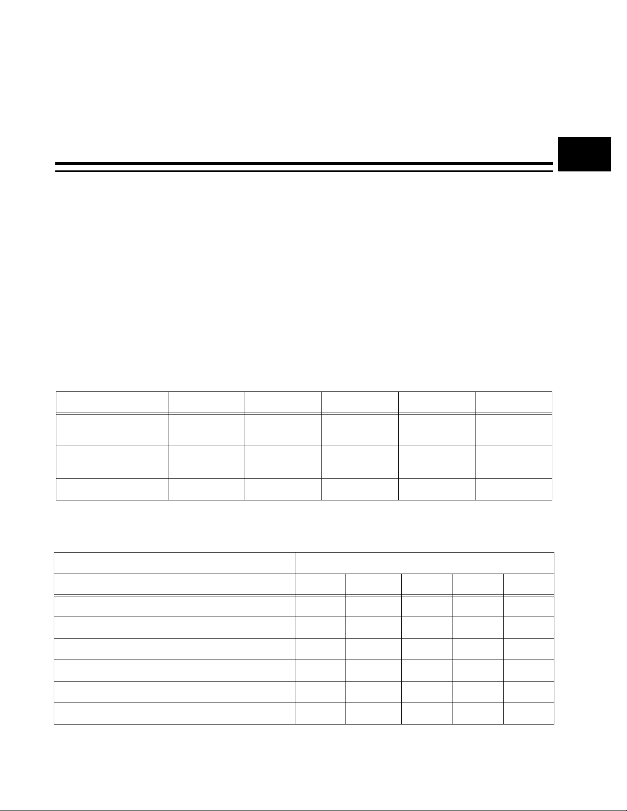
P
P
P
P.1 About the EP93xx User’s Guide
This EP93xx User’s Guide describes the architecture, hardwar e, and operation of the Cirrus
Logic EP9301, EP9302, EP9307, EP9312, and EP931 5 pr ocessors. It is i ntended t o be used
in conjunction with the respective EP93xx Data Sheets, which contain the full electrical
specifications for the EP93xx processors.
The EP9301, EP9302, EP9307, EP9312 processors are functional subsets of the EP9315
processor. All chapters in this Guide apply to the EP9315 processor. Most, but not all,
chapters apply to the EP9301, EP9302, EP9307, EP9312 processors. Table P-1 shows the
maximum core frequency and the maximum high-speed bus frequency as well as number of
package balls and package type for the EP93xx processors. Table P-2 shows chapter
numbers and function, and which EP93xx processors include the function (or not).
Ta ble P-1. F r eque ncy, Package, Applicable EP93xx Processor
EP9301 EP9302 EP9307 EP9312 EP9315
Chapter P 17Preface
Maximum Core
Frequency - MHz
Maximum High-Speed
Bus Frequency - MHz
Package Type
Table P-2. Chapter Number and Function, Applicable EP93xx Processor
Chapter Number and Function Applicable EP93xx Processor
0: Preface
1: Introduction
2: ARM920T Core and Advanced High-Speed Bus
3: MaverickCrunch Co-processor
4: Boot ROM
5: System Controller X X X X X
166 200 200 200 200
66 100 100 100 100
208 LQFP 208 LQFP 272 TFBGA 352 PBGA 352 PBGA
EP9301 EP9302 EP9307 EP9312 EP9315
X X XXX
X X XXX
X X XXX
- X XXX
X X XXX
DS785UM1 P-1
Copyright 2007 Cirrus Logic
Page 24

Preface
P
P
P
EP93xx User’s Guide
Table P-2. Chapter Number and Function, Applicable EP93xx Processor (Continued)
Chapter Number and Function Applicable EP93xx Processor
EP9301 EP9302 EP9307 EP9312 EP9315
6: Vectored Interrupt Controller X X X X X
7: Raster Engine with Analog and LCD Integrated
Timing and I nterface
8: Graphics Accelerator - - X - X
9: 1/10/100 Mbps Ethernet LAN Controller X X X X X
10: DMA Controller X X X X X
11: Universal Serial Bus Host Controllers 2 2 3 3 3
12: Static Memory Controller
Static Memory Controller with PCMCIA
13: SDRAM, SyncROM, SyncFLASH Controllers X X X X X
14: UART1 with Modem Control Signals and HDLC X X X X X
15: UART2 with IrDA X X X X X
16: UART3 with HDLC - - X X X
17: IrDA X X X X X
18: Timers 4 4 4 4 4
19: Watchdog Timer X X X X X
--XXX
X
-
X
-
X
-
X
-
-
X
20: Real Time Clock with Softw a re Trim X X X X X
2
21: I
S Controller
22: AC’97 Controller 1 1 1 1 1
23: Synchronous Serial Port 1 1 1 1 1
24: Pulse Width Modulators 2 2 1 2 2
25: Analog Touch Screen Interface/ADC 5-ADC 5-ADC 8-Wire TS 8-Wire TS 8-Wire TS
26: Keypad Interface - - X X X
27: IDE Interface - - - 2 Devices 2 Devices
28: GPIO Interface
29: Security
30: Glossary
P-2 DS785UM1
Copyright 2007 Cirrus Logic
3 3 333
X X XXX
X X XXX
X X XXX
Page 25

P
P
P
Note:“X” means Function is included; “-” means Function is not included
P.2 Related Documents from Cir rus Logic
1. EP9301 Data Sheet, Document Number - DS636PP5
2. EP9302 Data Sheet, Document Number - DS653PP3
3. EP9307 Data Sheet, Document Number - DS667PP4
4. EP9312 Data Sheet, Document Number - DS515PP7
5. EP9315 Data Sheet, Document Number - DS638PP1
P.3 Reference Documents
1. ARM®920T Technical Reference Manual, ARM Limited
2. AMBA Specification (Rev. 2.0), ARM IHI 0011A, ARM Limited
3. AHB Example AMBA System (Addendum 01), ARM DDI 0170A, ARM Limited
Preface
EP93xx User’s Guide
4. The co-processor instruction assembler notation can be referenced from ARM
programming manuals or the Quick Reference Card, document number ARM QRC
0001D, ARM Limited
5. The MAC engine is compliant with the requirement s of IS O/IEC 8802-3 (1993), Sections 3
and 4
6. OpenHCI - Open Host Controller interface Specification for USB, Release 1.0a;
®
Compaq
7. ARM Co-processor Quick Reference Card, document number ARM QRC 0001D, ARM
Limited
8. Information Technology, AT Attachment with Packet Interface - 5 (ATA/ATAPI-5) ANSI
NCITS document T13 1321D, Revision 3, 29 February 2000
9. ARM PrimeCell PL190-Rel1v1 Revision 1.7 Technical Reference Manual DDI0181C,
ARM Limited
10.Audio Codec ‘97, Revision 2.3, April 2002, Intel
, Microsoft®, National Semiconductor
P.4 Notational Conventions
This document uses the following conventions :
®
®
Corporation
• Internal and external Signal Names, and Pin Names use mixed upper and lower case
alphanumeric, and are shown in bold font, for example, RDLED
• Register Bit Fields are named using upper and lower case alphanumeric: for example,
SBOOT, LCSn1
DS785UM1 P-3
Copyright 2007 Cirrus Logic
Page 26

Preface
P
P
P
EP93xx User’s Guide
• Registers are named using mixed upper and lower case alphanumeric, for example,
SysCfg or PxDDR. Where there are multiple registers with the same names, a lower case
“x” is used as a place holder. For example, in the PxDDR registers, x represents a let ter
from A to H, indicating the specific port being discussed
CAUTION:In the Internal Register Map in “Internal Register Map” on page 2-17 some
(An example register description is shown below. This description is used for the following
examples.)
A specific bit may be specified in one of three ways:
1. Register name[bit number], for example, SysCfg[29]
2. Register name.bit field[bit number], for example, SysCfg.REV[1]
3. Register name.bit field[bit name], for example, SysCfg.SBOOT
Hexidecimal numbers are referred to as 0x0000_0000.
memory locations are listed as Reserved. These memory locations should not
be used. Reading from these memory locations will yield invalid data. Writing to
these memory locations may cause unpredictable results.
Binary numbers are referred to as 0000_0000b.
P.5 Register Example
Note:This is only an example. For actual SysCfg register information, see “SysCfg” on page 5-
34 .
SysCfg
31 30 29 28 27 26 25 24 23 22 21 20 19 18 17 16
REV RSVD
1514131211109876543210
RSVD SBOOT LCSn7 LCSn6 LASDO LEEDA LEECLK RSVD LCSn2 LCSn1
Address:
0x8093_009C - Read/Write, Softw are locked
Default:
0x0000_0000
Definition:
System Configuration Register. Provides various system configuration
options.
Bit Descriptions:
RSVD: Reserved. Unknown During Read.
P-4 DS785UM1
Copyright 2007 Cirrus Logic
Page 27

Preface
P
P
P
EP93xx User’s Guide
REV: Revision, reads chip Version number: 0 - Rev A, 1 - Rev B,
2 - Rev C, 3 - Rev D.
SBOOT: Serial Boot Flag. This bit is read-only.
1 hardware detected Serial Boot selection
0 hardware detected Normal Boot
LCSn7, LCSn6: Latched version of CSn7 and CSn6 respectively. These
are used to define the external bus wid t h for the boot code
boot.
LASDO: Lat ched ve rsion of ASDO pin. Used to select s ynchr onous
versus asynchronous boot device.
LEEDA: Latched version of EEDAT pin.
LEECLK: Define Internal or external boot:
1 Internal
0 External
LCSn1, LCSn2: Define Watchdog startup action:
0 0 Watchdog disabled, Reset duration disabled
0 1 Watchdog disabled, Reset duration active
1 0 Watchdog active, Reset duration disabled
1 1 Watchdog active, Reset duration active
DS785UM1 P-5
Copyright 2007 Cirrus Logic
Page 28

Preface
P
P
P
EP93xx User’s Guide
P-6 DS785UM1
Copyright 2007 Cirrus Logic
Page 29

1
1
1
1.1 Introduction
The EP93xx processors are highly integrated systems-on-a-chip that pave the way for a
multitude of next-generation consumer and industrial electronic pr oducts. Designers of digit al
media servers and jukeboxes, telematic cont rol systems, thin clients, set -top boxes, point-ofsale terminals, industrial controls, biometric security systems, and GPS devices will benefit
from the EP93x processors’ integrated architecture and advanced features. In fact, with
amazingly agile performance provided by a 166 or 200 MHz ARM920T Core, and featuring
an incredibly wide breadth of peripheral interfaces, the EP93xx processors are well suited to
an even broader range of high volume app lications. Furthermore, by ena bling or disabli ng the
EP93xx processor’s peripherals and their interf aces, designers can throttle power
consumption and reduce development costs and accelerate time-to-market by creating a
single platform that can be easily modified to deliver a variety of differentiated end products.
1.2 EP93xx Features
Chapter 1
1Introduction
Maximum clock rates plus package types and number of balls for EP93xx processors are
shown in Table 1-1.
Table 1-1. EP93xx Maximum Clock Rates, Package Type and Number of Balls
Processor Max Core Clock Rate
EP9301
EP9302
EP9307
EP9312
EP9315
Features of the EP93xx process ors are summarized in Table 1-2. Block diagrams are shown
in Figure 1-1 EP9301, Figure 1-2 EP9302, Figure 1-3 EP9307, Figure 1-4 EP9312, and
Figure 1-5 EP9315.
166 MHz 66 MHz 208 LQFP
200 MHz 100 MHz 208 LQFP
200 MHz 100 MHz 272 TFBGA
200 MHz 100 MHz 352 PBGA
200 MHz 100 MHz 352 PBGA
Max High-Speed Bus
Clock Rate
Package
DS785UM1 1-1
Copyright 2007 Cirrus Logic
Page 30
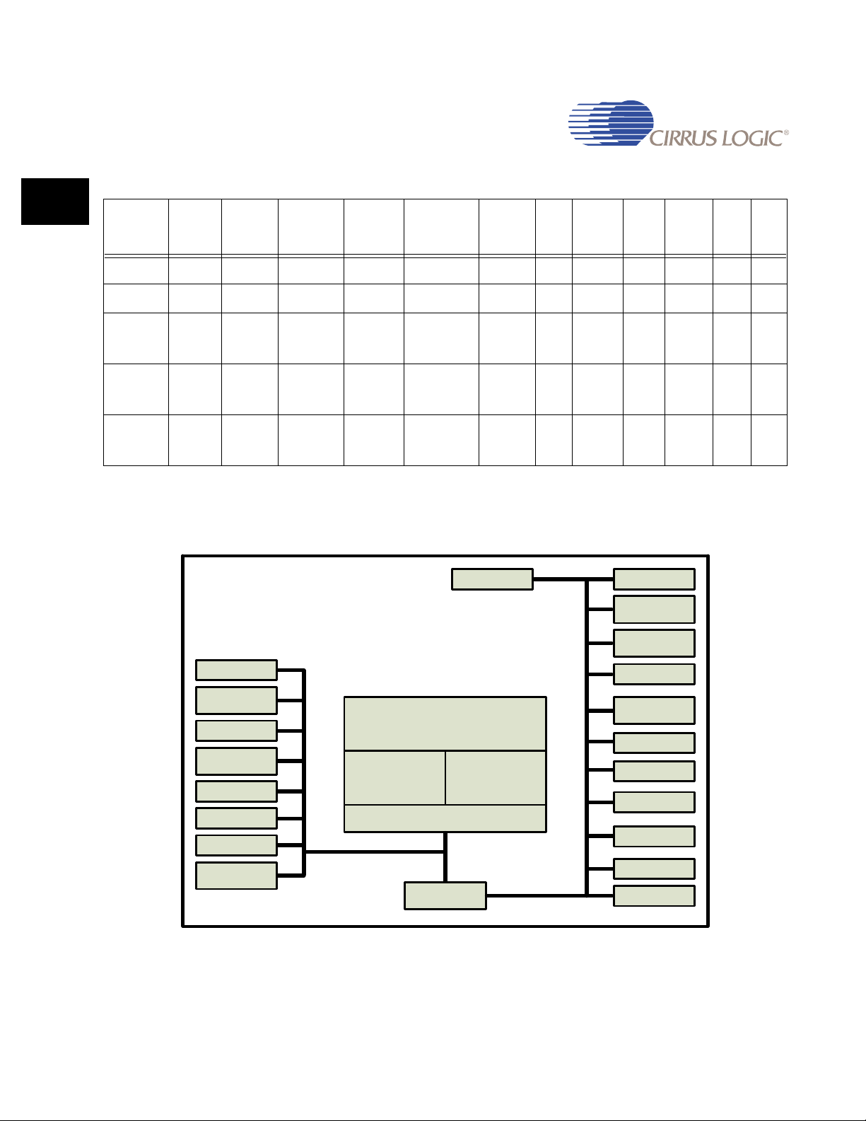
Introduction
1
1
1
EP93xx User’s Guide
Table 1-2. EP93xx Features Summary
Processor
EP9301 X - - - - X - 2 2 5-ADC 37 -
EP9302 X - X - - X - 2 2 5-ADC 37 -
EP9307 - X X X X X - 3 3
EP9312 - X X X - X 1 3 3
EP9315 - X X X X X 1 3 3
16-Bit
External
Bus
32-Bit
External
Bus
Math Co-
Processor
Raster
Analog /
LCD
2-D
Graphics
Accelerator
Ethernet
MAC
IDE
USB 2.0
Host
UART
Touch
Screen
/ ADC
8-Wire/
12-
ADC
8-Wire/
12-
ADC
8-Wire/
12-
ADC
GPIO
48 -
47 -
55 X
Note:“X” means that the function is included; “-” means that the function is not included.
UART2 with IrDA
UART1 with HDLC
System Control –
2 PLLs
PC
Card
SDRAM
SRAM, FLASH,
ROM
12 Channel DMA
1/10/100 Ethernet
MAC
JTAG
2 USB 2.0 FS Host
Boot ROM
Vectored
Inerrupts
ARM920T
I-Cache
16 KB
Memory Management Unit
High-Speed Bus (AHB)
AHB/APB Bridge
Figure 1-1. EP9301 Block Diagram
D-Cache
16 KB
Peripheral Bus (APB)
5-Channel ADC
2 PWM
Enhanced GPIO,
2-wire, 2 LED
I2S
SPI
AC’97
RTC with SW Trim
Watchdog Timer
4 Timers
1-2 DS785UM1
Copyright 2007 Cirrus Logic
Page 31

Introduction
1
1
1
EP93xx User’s Guide
SDRAM
SRAM, FLASH,
ROM
12 Channel DMA
1/10/100 Ethernet
MAC
JTAG
2 USB 2.0 FS Host
Boot ROM
Vectored
Inerrupts
UART2 with IrDA
MaverickCrunchTM Coprocessor
ARM920T
I-Cache
16 KB
Memory Manageme nt U nit
High-Speed Bus (AHB)
AHB/APB Bridge
D-Cache
16 KB
Peripheral Bus (APB)
Figure 1-2. EP9302 Block Diagram
UART1 with HDLC
System Control –
2 PLLs
5-Channel ADC
2 PWMs
Enhanced GPIO,
2-wire, 2 LED
I2S
SPI
AC’97
RTC with SW Trim
Watchdog Timer
4 Timers
2D Graphics
18-bit Raster LCD
plus CCITT656
Video
SDRAM
SRAM, FLASH,
ROM
12 Channel DMA
1/10/100 Etherne t
MAC
JTAG
3 USB 2.0 FS Host
Boot ROM
Vectored
Inerrupts
UART2 with IrDA
UART3 with HDLC
MaverickCrunchTM Coprocessor
ARM920T
I-Cache
16 KB
Memory Management Unit
High-Speed Bus (AHB)
AHB/APB Bridge
D-Cache
16 KB
Peripheral Bus (A PB )
Figure 1-3. EP9307 Block Diagram
UART1 with HDLC
System Control –
2 PLLs
8-Wire
Touchscreen ADC
8x8 Matrix Keypad
1 PWM
Enhanced GPIO
EEPROM, 2 LED
I2S
SPI
AC’97
RTC with SW Trim
Watchdog Timer
4 Timers
DS785UM1 1-3
Copyright 2007 Cirrus Logic
Page 32

Introduction
1
1
1
EP93xx User’s Guide
18-bit Raster LCD
plus CCITT656
Video
SDRAM
SRAM, FLA SH,
ROM
12 Channel DMA
1/10/100 Ethern et
MAC
JTAG
3 USB 2.0 FS Host
IDE
Boot ROM
Vectored
Inerrupts
UART2 with IrDA
UART3 with HDLC
MaverickCrunchTM Coprocess or
ARM920T
I-Cache
16 KB
Memory Management Unit
High-Speed Bus (AHB)
AHB/APB Bridge
D-Cache
16 KB
Peripheral Bus (APB)
Figure 1-4. EP9312 Block Diagram
UART1 with HDLC
System Contr o l –
2 PLLs
8-Wire
Touchscreen ADC
8x8 Matrix Keypad
2 PWMs
Enhanced GPIO,
2-wire, 2 LED
I2S
SPI
AC’97
RTC with SW Trim
Watchdog Timer
4 Timers
2D Graphics
18-bit Raster LCD
plus CCITT656
Video
SDRAM
SRAM, FLASH,
ROM, PCMCIA
12 Channel DMA
1/10/100 Ethernet
MAC
JTAG
3 USB 2.0 FS Host
2 IDE
Boot ROM
Vectored
Inerrupts
UART2 with IrDA
UART3 with HDLC
MaverickCrunchTM Coprocessor
ARM920T
I-Cache
16 KB
Memory Management Unit
High-Speed Bus (AHB)
AHB/APB Bridge
D-Cache
16 KB
Peripheral Bus (APB)
Figure 1-5. EP9315 Block Diagram
UART1 with HDLC
System Control –
2 PLLs
8-Wire
Touchscreen ADC
8x8 Matrix Keypad
2 PWMs
Enhanced GPIO,
2-wire, 2 LED
I2S
SPI
AC’97
RTC with SW Trim
Watchdog Timer
4 Timers
1-4 DS785UM1
Copyright 2007 Cirrus Logic
Page 33

Introduction
1
1
1
EP93xx User’s Guide
Features of the EP93xx processors are:
• ARM920T Core:
• 200 MHz maximum run frequency and 100 MHz maximum high-speed bus frequency
for EP9302, 9307, 9312, and 9315 only
• 166 MHz maximum run frequency and 66 MHz maximum high-speed bus frequency for
EP9301 only
• 16 KByte instruction cache and 16 KByte data cache
• Memory Management Unit (MMU) with 64-entry Translation-Lookaside-Buffers (TLBs)
®
enable Linux
• MaverickCrunch™ Co-processor in EP9302, 9307, 9312, and 9315 only:
• Floating point, integer and signal processing instructions
• Optimized for digital mu sic compression algorithms
• Hardware interlocks allow in-line coding
and Windows® CE
®
™
• MaverickKey
• 32-bit unique ID
• 128-bit random ID
• Integrated Peripherals and Interfaces:
• EIDE, up to 2 devices in EP9312 and 9315 only
• 1/10/100 Mbps Ethernet MAC
• Two-port USB 2.0 Full Speed host (OHCI) in EP9301 and 9302 only
• Three-port USB 2.0 Full Speed host (OHCI) in EP9307, 9312, and 9315 only
• IrDA controller, slow and fast mode
• Two UARTs (16550 Type) in EP9301 and 9302 only:
• - UART1 (optionally supports on- chip handling of HDLC)
• - UART2 (optionally provides interface for IrDA controller)
• Three UARTs (16550 Type) in EP9307, 9312, and 9315 only:
- UART1 and UART3 (optionally suppo rt on-chip handling of HDLC)
- UART2 (optionally provides interface for IrDA controller)
IDs for Digital Rights Management or Design IP Security:
- UART3 implements both a UART and an HDLC interface identical to that of UART1;
• LCD and Analog Raster Interface in EP9307, 9312, and 9315 only
• 2D Graphics Accelerator in EP9307and 9315 only
- Line Draw
DS785UM1 1-5
Copyright 2007 Cirrus Logic
Page 34

Introduction
1
1
1
EP93xx User’s Guide
- Block Copy
- Block Fill
• Touch Screen interface
- 5-ADC in EP9301 and 9302 only
- 8-Wire Touch Screen/ADC in EP9307, 9312, and 9315 only
• SPI port
• AC ‘97 interface
2
S interface with up to 6 channels
•I
• 8x8 Matrix keypad scanner (in EP9307, EP9312, and EP9315 only)
• PCMCIA Interface supporting 8-bi t or 16-bit PCMCIA (PC Card) devices in EP9315 only
• External Memory Options
• 16-bit SDRAM interface (up to 4 banks) in EP9301 and 9302 only
• 32-bit SDRAM interface (up to 4 banks) in EP9307, 9312, and 9315 only
• 16/8-bit SRAM/Flash/ROM interface in EP9301 and 9302 only
• 32/16/8-bit SRAM/Flash/ROM interface in EP9307, 9312, and 9315 only
• Serial Flash interface
• Internal Peripherals
• Real-Time cl ock with software trim
• 12 DMA channels for data transfer to maximize system performance
• Boot ROM
• Dual PLLs
• Watchdog timer
• Two general purpose 16-bit timers
• General purpose 32-bit timer
• 40-bit debug timer
• Standard General-Pur pose I/Os (GPI Os ), no interrupts:
• 18 in EP9301 and 9302 only
• 30 in EP9307 only
• 31 in EP9312 and 9315 only
• Enhanced General-Purpose I/Os (EGPIOs) plus Port F GPIOs can generate interrupts:
• 19 in EP9301, 9302 only
• 18 in EP9307 only
1-6 DS785UM1
Copyright 2007 Cirrus Logic
Page 35

1
1
1
• 16 in EP9312 only
• 24 in EP9315 only
1.3 EP93xx Processor Applications
The EP93xx processors can be used in a variety of applications, such as:
• Digital media servers
• Integrated home media gateways
• Digital audio jukeboxes
• Streaming audio/video players
• Telematic control systems
• Set-top boxes
• Point-of -s a le terminals
• Thin clients
Introduction
EP93xx User’s Guide
• Internet TVs
• Biometric security systems
• Industrial controls
• GPS & fleet management systems
• Educational toys
• Voti ng ma chines
• Medical equipment
1.4 EP93xx Processor Highlights
1.4.1 High-Performance ARM920T Core
The EP93xx Processors feature an advanced ARM920T Core design with an MMU that
supports Linux
ARM920T’s 32-bit microc ontrol ler ar chitec tur e, wit h a five- st age pi pelin e, d eliver s i mpres sive
performance at very low power. The included 16 KByte instruction cache and 16 KByte data
cache provide zero-cycle latency to th e current program and data, or can be locked to
provide guaranteed no-latency access to cr itical instructions and data . For applications with
instruction memory size restrictions, the ARM920T’s compressed Thumb
provides a space-eff icient design that maximizes external instru ction memory usage.
®
, Windows® CE®, and many other embedded operating systems. The
®
instruction set
1.4.2 MaverickCrunch™ Co-processor for Ultra-Fast Math Processing
The EP9302, EP9307, EP9312, and EP9315 processors include an advanced
MaverickCrunch co-processor that pr ovides mixed-mode math functions to greatl y accelerate
the floating-point processing capabilities of the ARM920T Core. The MaverickCrunch co-
DS785UM1 1-7
Copyright 2007 Cirrus Logic
Page 36

Introduction
1
1
1
EP93xx User’s Guide
processor simplifies the end-user’s programming task by using predefined co-processor
instructions, utilizing standard ARM compiler tools, and by requiring just one debugger
session for the entire system. Furthermore, the integrated design provides a single
instruction stream and t he advantage of zero latenc y for cached instructions. To emulate this
capability, competitors’ solutions add a DSP to the system, which requires separate
compiler/linker/debugger tool sets. This additional DSP requires programmers to write two
separate programs and debug them simult aneously, which can result in frustration and costly
delays.
1.4.3 MaverickKey™ Unique ID Secures Digital Content in OEM Designs
The EP93xx processors include Mav erickKey uni que hardware pr ogrammed IDs that pr ovide
an excellent solution to the growing concern over secure Web content and commerce. With
Internet security playing an impor tant role in the delivery of digital media such as books or
music, traditional software methods are quickly becoming unreli able. The MaverickKey
unique IDs provide OEMs with a method of utilizing specific hardware IDs for DRM (Digital
Rights Management) and other authentication mechanisms.
MaverickKey uses a specific 32-bit ID and a 128-bit random ID that are programmed into the
EP93xx processors through the use of l aser pr obing technology. These IDs can then be used
to match secure copyrighted content with the ID of the tar get device that the EP93xx
processor is powering, and then deliver the copyright ed information over a secure
connection. In addition, secure transac tions can benefit by matching device IDs to server IDs.
MaverickKey IDs can also be used by OEMs and design houses to protect against design
piracy by presetting ranges for unique IDs . For more i nformation on securing your design
using MaverickKey, please contact your Cirrus Logic sales representat ive.
1.4.4 Integrated Multi-Port USB 2.0 Full Speed Hosts with Transceivers
The EP9307, EP9312, and EP9315 processors integrate three USB 2.0 Full Speed Host
ports while the EP9301 and EP9302 integrate two of the ports. Fully compliant to the OHCI
USB 2.0 Full Speed specification (12 Mbps), the host por ts can be used to provide
connections to a number of external devices including mass storage devices, external
portable devices suc h as audio p layers or camera s, printers , or USB hubs. Naturally, the USB
host ports support the USB 2.0 Low Speed standard as well. This prov ides the oppor tun ity to
create a wide array of flexible system configurations.
1-8 DS785UM1
Copyright 2007 Cirrus Logic
Page 37

1
1
1
1.4.5 Integrated Ethernet MAC Reduces BOM Costs
The EP93xx processors integrate a 1/10/ 100 Mbps Ethernet Media Acc ess Controller ( MAC).
With a simple connection to MII-based external PHYs (such as the Cirrus Logic CS8952 PHY
Transceiver) , an EP93xx processor-based sys tem has easy , hi gh-performance, cost-e ffective
Internet capability.
1.4.6 8x8 Keypad Interface Reduces BOM Costs
The EP9307, 9312, and 9315 processors include a matrix keypad control ler that scans an
8x8 array of 64 normally open, single pole switches. Any one or two keys depressed will be
de-bounced and decoded. An interrupt i s generated whenever a stable set of depressed key s
is detected. If the keypad is not utilized, the 16 column/row pins may be used as generalpurpose I/Os.
1.4.7 Multiple Booting Mechanisms Increase Flexibility
The EP93xx processors include a 16 KByte Boot ROM to set up st andard configur ations. The
Boot ROM controls booting from either FLASH memory, the SPI serial interface, or a UART.
This boot flexibility makes it easy to desi gn user-controlled, field-upgradable systems. See
Chapter 4 on page 4-1, for additional details. The EP93xx processors can also boot directly
from CSn0, bypassing the Boot ROM.
Introduction
EP93xx User’s Guide
1.4.8 Abundant General Purpose I/Os Build Flexible Systems
The EP93xx processors include both enhanced and standard general-purpose I/O pins
(GPIOs). The enhanced GPIOs may individually be configured as inputs, outputs, or
interrupt-enabled input s. Ni neteen enhanc ed GPIOs ar e in EP9301 and 9302 processor s, 18
are in the EP9307 processor, and 16 are in EP9312 processor, and 24 are in the EP9315
processor.
The standard GPIOs may individually be used as inputs, outputs, or (in some cases) opendrain pins. The standard GPIOs are multiplexed with peripheral function pins, so the number
available depends on the utilization of peripherals. Eighteen standard GPIOs are in EP9301
and 9302 processors, 30 are in the EP9307 processor, 31 are in the EP9312 and EP9315
processors.
Together, the enhanced and standard GPIOs facili tate easy system design with external
peripherals not integrated on the EP93xx processors.
1.4.9 General-Purpose Memory Interface (SDRAM, SRAM, ROM, FLASH)
The EP93xx processors feature a unified memory address model in which all memory
devices are accessed over a common address/data bus. In the EP9301 and 9302
processors, the common address/data bus is 16-bits wide, the Static Memory Controller
(SMC) supports 8-bit and 16-bit devices and the SDRAM, SyncROM, and SyncFLASH
synchronous memory controller supports 16-bit devices. In the EP9307, EP9312, and
EP9315 processors, the common address/data bus is programmable to either 16-bits or 32-
DS785UM1 1-9
Copyright 2007 Cirrus Logic
Page 38

Introduction
1
1
1
EP93xx User’s Guide
bits wide, the SMC supports 8-bit, 16-bit, and 32-bit devices, and the SDRAM, SyncROM,
and SyncFLASH synchronous memory controller supports 16-bit and 32-bit devices. In the
EP9307, EP9312, and EP9315 processors, a separate internal bus to the dynamic memory
controller is dedicated to the read-only Raster/Display refresh engine.
1.4.10 12-Bit Analog-to-Digital Converter (ADC) Provides an Integrated Touch-Screen Interface or General ADC Functionality
The EP9301 and EP9302 processors include a 5-channel ADC. The EP9307, EP9212, and
EP9315 processors include a 12-bit ADC, which can be utilized eit her as an 8-wire touchscreen interface or for general ADC functionality. The touch-screen interface performs all
sampling, averaging, ADC range checking, and control for a wide variety of analog-resistive
touch screens. To improve system performance, the controller only interrupts the ARM Core
when a meaningful change occurs. The touch screen hardware may be disabled , and the
switch matrix and ADC controlled directly for general ADC usage if desired.
1.4.11 Raster Analog / LCD Controller
The EP9307, EP9312, and EP9315 processors include a raster/LCD controller that features
fully programmable video interface timing for either non-interlaced or dual scan color and
grayscale flat panel displa ys. Resoluti ons up to 1024 x768 pixels are suppor ted from a uni fied
SDRAM-based frame buffer with pixel depths of 4, 8, 16, or 18 bits. A 256x18 color lookup
table, a hardware blinking cursor with up to 64x64 pixels, and an interface to smart panel
displays is also included.
1.4.12 Graphics Accelerator
The EP9307 and EP9315 processors include a hardware graphics acceleration engine that
improves graphic performance by handling block copy, block fill and hardware line draw
operations. The graphics accele rator is used to off load graphics operations from the ARM
Core.
1.4.13 PCMCIA Interface
The EP9315 processor (only) provides a PCMCIA interface that supports 8-bit or 16-bit
PCMCIA PC Cards. These PCMCIA cards are credit card si zed peripherals that add memory,
mass storage and I/O capabilities to compute r syst ems, and can be u sed to further broaden
the options of a designer’s platform.
1-10 DS785UM1
Copyright 2007 Cirrus Logic
Page 39

2
2
2
Chapter 2
2ARM920T Core and Advanced High-Speed Bus (AHB)
2.1 Introduction
This chapter describes the ARM920T Core and the Advanced High-Speed Bus (AHB).
2.2 Overview: ARM920T Core
The ARM920T is a Harvard architecture core with separate 16 kbyte instruction and data
caches with an 8-word line length. The ARM Core utilizes a five-stage pipeline consisting of
fetch, decode, execute, data me mory access, and write stages.
2.2.1 Features
Key features include:
• ARM V4T (32-bit) and Thumb (16-bit compressed) instruction sets
• 32-bit Advanced Micro-Controller Bus Architecture (AMBA)
• 16 kbyte Instruction Cache with lockdown
• 16 kbyte Data Cache (programmable write-through or write-back) wit h lockdown
• Write Buffer
• MMU for Microsoft Windows CE and Linux operating systems
• Translation Look-aside Buffers (TLB) with 64 Data and 64 Instruction Entries
• Programmable Page Sizes of 64 kbyte, 4 kbyte, and 1 kbyte
• Independent lockdown of TLB Entries
• JTAG Interface for Debug Control
• Co-processor Interface
DS785UM1 2-1
Copyright 2007 Cirrus Logic
Page 40

ARM920T Core and Advanced High-Speed Bus (AHB)
2
2
2
EP93xx User’s Guide
2.2.2 Block Diagram
External
Co-Proc
Interface
JTAG
Instruction
cache
R13
ARM9TDMI
Processor core
(Integral
EmbeddedICE)
R13
Data cache Data MMU
Instruction
MMU
CP15
Write
Buffer
Write Back
PA TAG
RAM
AMBA
Bus
Int.
APB
Figure 2-1. ARM920T Block Diagram
2.2.3 Operations
The ARM920T core follows a Harvard architecture and consists of an ARM9TDMI core,
MMU, instruction and data cache. The core supports both the 32-bit ARM and 16-bit Thumb
instruction sets.
The internal bus structure (AMBA) inclu des both a high speed and l ow speed bu s. The high
speed bus AHB (Advanced High-performance Bus) contains a high speed i nternal bus clock
to synchronize co-processor, MMU, cache, DMA controller, and memory modules. AMBA
includes a AHB/APB bridge to the lower speed APB (Advanced Peripheral Bus). The APB
bus connects to lower speed peripher al devices such as UARTs and GPIOs.
The MMU provides memory address translation for all memory and peripherals designed to
remap memory devices and peripheral address locations. Sections, large, small and tiny
pages are programmable to map memory in 1 Mbyte, 64 kbyte, 4 kbyte, 1 kbyte size blocks.
To increase system performance, a 64-entry translation look-aside buffer will cache 64
address locations before a TLB miss occurs.
2-2 DS785UM1
Copyright 2007 Cirrus Logic
Page 41

2
2
2
A 16 kbyte instruction and a 16 kbyte data cache are included to increase performance for
cache-enabled memory regions. The 64-way associative cache also has lock-down
capability. A 16-word Write Buffer all ows cached ins tructions to be fetched and decoded while
the Write Buffer send s data to external memory.
The ARM920T Core supports a number of co-processors, including the MaverickCrunch coprocessor by means of a specific pipeline architecture interface.
2.2.3.1 ARM9TDMI Core
ARM9TDMI core is responsible fo r execut ing both 32- bit ARM and 16-bi t Thumb inst ructions.
Each provides a unique advantage to a system design. Internally, the instructions enter a 5stage pipeline. These stages are:
• Instruction Fetch
• Instruction Decode
• Execute
• Data Memory Access
ARM920T Core and Advanced High-Speed Bus (AHB)
EP93xx User’s Guide
• Register Write
All instructions are fully interlocked. This mechanism will delay the execution st age of a
instruction if dat a in that i nstruction comes from a previ ous instruction that is no t available y et.
This simply insures that software will function identically across different implementations.
For memory access instructions, t he base register used for the access wil l be restor ed by the
ARM Core in the event of an Abort exception. The base register will be restored to the value
contained in it immediately before execution of the instruction.
The ARM9TDMI core memory interface includes a separate inst ruction and data interface to
allow concurrent access of instructions and data to reduce the number of CPI (cycles per
instruction). Both inter faces use pipeline addressing. The core can operate in big and li ttle
endian mode. Endianess affects both the address and the data interfaces.
The memory interface executes four types of memory transfers: sequential, non-sequential,
internal, and co-processor. It will also support uni- and bi-directional transfer modes.
The core provides a debug interface called JTAG (Joint T esting Act ion Group). This inter face
provides debug capability with five external control signals:
• TDO - Test Data Out
• TDI - Test Data In
• TMS - Test Mode Select
• TCK - Test Clock
• nTRST - Te st Reset
There are six scan chains (0 through 5) in the ARM9TDMI controlled by the JTAG Test
Access Port (TAP) controller. Details on the individual scan chain function and bit order can
be found in the ARM920T Technical Reference Manual.
DS785UM1 2-3
Copyright 2007 Cirrus Logic
Page 42

ARM920T Core and Advanced High-Speed Bus (AHB)
2
2
2
EP93xx User’s Guide
2.2.3.2 Memory Management Unit
The MMU provides the translat ion an d acc ess permissi ons for t he address and dat a po rt s f or
the ARM9TDMI core. The MMU is controlled by page tabl es stor ed in system memory and
accessed using the CP15 register 1. The main features of the MMU are as follows:
• Address Translation
• Access Permissions and Domains
• MMU Cache and Write Buffer Access
2.2.3.2.1 Address Translation
The virtual address from the ARM920T c ore is modified by R13 internally to create a modified
virtual address. The MMU then tr anslates th e modifi ed vir tual add ress from R13 by the CP15
register 3 into a phys ical addres s t o access exte rnal memory or a de vice. The MMU l ooks for
the physical address from the Translation Table Base (TTB) in system memory. It will also
update the TLB cache.
The TLB is two 64-entry caches, one for data and one for instruction. If the physical address
for the current virtual addr ess is not found in the TLB (miss) , the ARM Core wi ll go to ext ernal
memory and look for the TTB in system memory. The internal translation table walks
hardware steps thro ugh the p age t able s etup in exte rnal memory for the appro pri ate physical
address.
When the physical address is acquired, the TLB is updated. Whe n the address is found in the
TLB, system performance will increase s ince additi onal cycl es to access memory and update
the TLB are avoided.
Translation of system memory is done by breaking up the memory into different size blocks
called sections, lar ge p ages, small p ages, and tiny p ages. Syst em memory and regi ster s ca n
be remapped by the MMU. The block sizes are as follows:
• Section - 1 Mbyte
• Large Page - 64 kbyte
• Small Page - 16 kbyte
• Tiny Page - 1 kbyte
2.2.3.2.2 Access Permission and Domains
Access to any section or page of memory is dependent on it s domain. The page table in
external memory also contains access permissions for all sub-divisions of external memory.
Access to specific instructi ons or data has three possible states:
• Client: Access permissions based on the section or page table descriptor
• Manager: Ignore access permissions in the section or p age table descriptor
• No access: any attempted access generates a domain fault
2-4 DS785UM1
Copyright 2007 Cirrus Logic
Page 43

2
2
2
2.2.3.2.3 MMU Enable
Enabling the MMU allows system memory control, but is also required if the Dat a Ca che and
the Write Buf fer are to be used. Feat ures are enabled f or specific memory r egions, as defined
in the system page tabl e. MMU enablemen t is done via CP15 re gis ter 1. The pr ocedu re is as
follows:
1. Program the Translation Table Base (TTB) and domain access control registers
2. Create level 1 and level 2 pages for the system, and enable the Data Cache and the
Write Buffer
3. Enable the MMU via bit 0 of CP15 register 1.
2.2.3.3 Cache and Write Buffer
Cache configuration i s 64-way se t assoc iative. The re i s a 16 k byte inst ruction cache and a 16
kbyte data cache. The caches have the following characteristics:
• 8 words per line, with 1 valid bit and 2 dirty bits per line to allow half-line write-backs
ARM920T Core and Advanced High-Speed Bus (AHB)
EP93xx User’s Guide
• Write-through or write-back capability, selectable per memory region defined by the
MMU
• Pseudo random or round robin replacement algorithms for cache misses. This is
determined by the RR bit (bit 14 ) in CP15 register 1. On a cache miss (i nstructi on or dat a
not in the respective cache), an 8-word line is fetched from memory and loaded into the
cache
• Independent cache lock-down with granularity of 1/64th of total cache size or 256 bytes
for both instructions and data. Lock-down of the cache will prevent an eight-word cache
line fill into that region of the cache
• For compatibility with Windows CE and to reduce latency, physical addresses for data
cache entries are stored in the PA TAG RAM, which is used for cache line write-back
operations without need of the MMU. This prevents a possible TLB miss that would
degrade performance
• The Write Buffer has a depth of 16 data words. If enabled, writes are sent to the Write
Buffer directly from the Data Cache or from the CPU (in the event of a cache miss or if
the cache is not enabled).
2.2.3.3.1 Instruction Cache Enab le
• At reset, the Instruction Cache is disabled
• A write to bit 12 of CP15 register 1 will enable or disable the Instruction Cache. If the
Instruction Cache (I-Cache) is enabled without the MMU enabled, all accesses are
treated as cacheable
• If the I-Cache is disabled, current contents are ignored. If re-enabled before a reset,
contents will be unchanged, but may not be coherent with eternal memory. If so,
contents must be flushed before re-enabling.
DS785UM1 2-5
Copyright 2007 Cirrus Logic
Page 44

ARM920T Core and Advanced High-Speed Bus (AHB)
2
2
2
EP93xx User’s Guide
2.2.3.3.2 Data Cache Enable
• A write to bit 2 of CP15 register 1 will enable or di sable the Data Cache (D-Cache)/Write
Buffer
• The D-Cache may only be enabled when the MMU is enabled. All data accesses are
subject to MMU and permission checks
• If disabled, current contents are ignored. If re-enabled before a reset, contents will be
unchanged, but may not be coherent with external memory. Depending on system
software, a clean and invalidate action may be required before re-enabling.
2.2.3.3.3 Write Buffer Enable
• The Write Buffer is enabled via the page table entries in the MMU. The Write buffer
cannot be enabled unless the MMU is enabled.
2.2.4 Co-processor Interface
The MaverickCrunch co-processor is explained in detail in Chapter 3 on page 3-1. The
relationship between the ARM co-processor instructions and MaverickCrunch co-processor
is also explained in Chapter 3.
The ARM co-processor instruction set includes:
• LDC - Load co-processor from memory
• STC - Store co-processor register from memory
• MRC - Move to ARM register from co-processor register
• MCR - Move to co-processor register from ARM register
The ARM co-processor has sixteen (C0 through C15) 64-bit reg ist ers for data transfer and
data manipulation. See Chapter 3, Section 3.2 on page 3-8 for a code example.
2.2.5 AMBA AHB Bus Interface Overview
The AHB (Advanced High-Performance Bus) is the high-per fo rmance syste m backbone bus .
Figure 2-2 on page 2-7 shows a typical AMBA AHB System.
The AHB connects devices that require high bandwi dth, such as DMA controllers, external
memory, and co-processors. The AHB supports:
• Burst Transactions
• Split Transactions
• Bus Master hand-over to devices such as the MaverickCrunch co-processor or DMA
controller
• Single clock edge operations
The APB (Advanced Peripheral Bus) is a lower bandwidth, but lower power, bus that
provides:
2-6 DS785UM1
Copyright 2007 Cirrus Logic
Page 45

2
2
2
• Latched address and control
• A simple Interface to on-chip peripherals such as UARTs and AC’97.
ARM9TD MI
External
Memory
Interf ac e
Figure 2-2. Typical AMBA AHB System
2.2.6 AHB Implementation Details
ARM920T Core and Advanced High-Speed Bus (AHB)
EP93xx User’s Guide
Co-
Processo
USB
r
AHB APB
DMA
Controller
AHB/
APB
B
r
i
d
g
e
UART SPI
GPIO
AC97
Peripherals or the external memory interface that have high bandwidth and low latency
requirements are connected to the CPU using the AHB bus. The peripherals include the
Vectored Interrupt Controllers (VIC1, VIC2), DMA, LCD/Raster registers, USB host, IDE,
Ethernet MAC and the bridge to the APB interface. The AHB/APB Bridge transparently
converts the AHB accesses into the slower speed APB accesses. All of the control registers
for the APB peripherals are programmed using the AHB/APB bridge interface. The main AHB
data and address lines are configure d using a multiplexed bus. This removes the need for
three state buffers and bus holders, and simplifies bus arbitration. Figure 2-3 on page 2-8
shows the main data paths in the processor’s AHB implementation.
DS785UM1 2-7
Copyright 2007 Cirrus Logic
Page 46

ARM920T Core and Advanced High-Speed Bus (AHB)
2
2
2
EP93xx User’s Guide
Ethernet
ARM920T
VIC2
VIC1
APB
18 Bit Raster
LCD I/F
SDRAM
Controller
E
B
I
Static
Memory/
PCMCIA
IDE
USB
Host
AHB
Maverick
Crunch
Boot ROM
DMA
UARTs
Timers
AHB/APB
bridge
RTC
Watchdog
Test
Support
Touchscreen
8x8 Key Mtx
GPIOs
PWM
SPI
I2S
IrDA
PLL1 PLL2
Clock & State
Control
AC97
Figure 2-3. Main Data Paths
Before an AMBA-to-AHB transfer can commence, the bus ma ster must be gran ted access t o
the bus. This process is started by the master asserting a request signal to the Arbiter. The
Arbiter then indicates when the master will be granted use of the bus. A granted bus master
starts an AMBA-to-AHB transf er by driving the address and control signals. These signals
provide information on the address, direction and width of the transfer, as well as indicating
whether the transfer is part of a burst.
Two different forms of burst transfers are al lowed:
• Incrementing bursts, which do not wrap at address boundaries
• Wrapping bursts, which wrap at particular address boundaries.
2-8 DS785UM1
Copyright 2007 Cirrus Logic
Page 47

2
2
2
A write data bus is used to move data from the master to a slave, while a read data bus is
used to move data from a slave to the master. Every transfer consists of:
• An address and control cycle
• One or more cycles for the data.
In normal operation a master is allowed to complete all the transfers in a particular burst
before the arbiter grants another master access to the bus. However, in order to avoid
excessive arbitration latencies, it is possible for the arbiter to break up a burst, and, in such
cases, the master must re- arbit rate for the bus i n order t o complete the remaini ng tr ansfers i n
the burst.
2.2.7 Memory and Bus Access Errors
There are several possible sources of access errors:
• Reads to reserved or undefined register memory addresses will return indeterminate
data. Writes to reserved or undefined memory addresses are generally ignored, but this
behavior is not guaranteed. Many register addresses are not fully decoded, so aliasing
may occur. Addresses and memory ranges listed as Reserved should not be accessed;
access behavior to these regions is not defined
ARM920T Core and Advanced High-Speed Bus (AHB)
EP93xx User’s Guide
• Access to non-existent registers or memory may result in a bus error
• Any access to the APB control register space will complete normally, as these devices
have no means of signaling an error
• Access to non-existent AHB or APB registers may result i n a bus error, depending on the
device and nature of the error. Device specific access rules are defined in the device
descriptions
• External memory access is controlled by the Static Memory Controller (SMC) or the
Synchronous Dynamic RAM (SDRAM) controller. In general, access to non-existent
external memory will complete normally, with reads returning random false data.
2.2.8 Bus Arbitration
The arbitration mechanism is used to ensure t hat only o ne maste r has access to t he bus that
it controls at any one time. The Arbiter performs this function by observing a number of
different requests to use the bus, and then deciding which is currently the highest priority
master requesting the bus.
The arbitration scheme can be broken down into three main areas:
• The main AHB system bus Arbiter
• The SDRAM slave interface Arbiter
• The EBI bus Arbiter
DS785UM1 2-9
Copyright 2007 Cirrus Logic
Page 48

ARM920T Core and Advanced High-Speed Bus (AHB)
2
2
2
EP93xx User’s Guide
2.2.8.1 Main AHB Bus Arbiter
This Main AHB Bus Arbiter controls bus master arbitration for the AHB bus. The AHB bus has
eight master interfaces:
• ARM920T
• DMA controller
• USB hosts (USB1, 2, 3)
• Ethernet MAC
• LCD/Raster
• Raster Hardware Cursor.
These interfaces have an order of priority that is linked closely with the power saving modes
Halt and Standby. These power saving modes force the Arbiter to gr ant the default bus
master , in this case, the ARM920T.
The order of priority of the bus masters, from highest to lowest, is shown in Table 2-1.
Table 2-1. AHB Arbiter Priority Scheme
Priority
Number
1 Raster Cursor Raster Raster Raster
2 MAC Raster Cursor Raster Cursor DMA
3 USB MAC DMA MAC
4 DMA USB USB USB
5 ARM920T ARM920T MAC Raster Cursor
6 Raster DMA ARM920T ARM920T
The priority of the arbiter may be programmed via the BusMstrArb register in the Clock and
St ate Control ler. The arbiter can also be programmed to degrant one of these masters: DMA,
USB Host or Ethernet MAC if an interrupt (IRQ or FIQ) is pending or bei ng serviced. This
prevents one of these masters from blocking important interrupt service routines. These
masters are thereby prevented from accessing the bus, that is, their bus requests are
masked until the IRQ/FIQ is removed (by the Interrupt Service Routine). After the IRQ/FIQ is
removed, their bus requests wi ll again be r ecognize d. The default is to progr am the arbiter so
that it does not degrant any of these masters.
In normal operation, when the ARM920T is grant ed the bus and a request to enter Hal t mode
is received, the ARM920T is de-granted from the AHB bus. Any other master reque sting the
bus during Halt mode (according to it’ s priority) will be granted the bus. In the case of entry
into Standby mode, the dummy master will be granted the bus, which simply performs IDLE
transfers. In this way, all the masters except the ARM920T can be used during Halt mode, but
are shutdown upon entry into Standby mode.
PRIORITY 00
(Reset value)
PRIORITY 01 PRIORITY 10 PRIORITY 11
2-10 DS785UM1
Copyright 2007 Cirrus Logic
Page 49

2
2
2
2.2.8.2 SDRAM Slave Arbiter
The SDRAM Slave Arbiter prioritizes between accesses from the AHB bus and the Raster
DMA bus. If an access request from the AHB arrives at the same time as an access request
from the Raster DMA, the Raster DMA will be given access while the AHB request is queued.
2.2.8.3 EBI Bus Arbiter
The EBI Bus Arbiter is used to arbitrate between accesses from the SDRAM controller and
the Static Memory controller, where priority is given to accesses from the SDRAM controller.
2.3 AHB Decoder
The AHB Decoder contains t he device memory map f or all of the AHB mast ers/slaves and for
the APB bridge. When a particular address range is sel ected, the appropriate signal is
generated as defined in Table 2-2.
(For additional information, see 17, “Reference Documents” on page P-3.
ARM920T Core and Advanced High-Speed Bus (AHB)
EP93xx User’s Guide
Table 2-2. AHB Peripheral Address Range
Address Range Register Width Peripheral Type Peripheral
0x800D_0000 - 0x800F_FFFF - - Reserved
0x800C_0000 - 0x800C_FFFF 32 AHB VIC2
0x800B_0000 - 0x800B_FFFF 32 AHB VIC1
0x800A_0000 - 0x800A_FFFF 32 AHB IDE
0x8009_0000 - 0x8009_FFFF 32 AHB Boot ROM physical address
0x8008_0000 - 0x8008_FFFF 32 AHB SRAM Controller/ PCMCIA
0x8007_0000 - 0x8007_FFFF - - Reserved
0x8006_0000 - 0x8006_FFFF 32 AHB SDRAM Controller
0x8005_0000 - 0x8005_FFFF - - Reserved
0x8004_0000 - 0x8004_FFFF - - Reserved
0x8003_0000 - 0x8003_FFFF 32 AHB Raster
0x8002_0000 - 0x8002_FFFF 32 AHB USB Host
0x8001_0000 - 0x8001_FFFF 32 AHB Ethernet MAC
0x8000_0000 - 0x8000_FFFF 32 AHB DMA
Note: Due to decoding optimization, the AHB peripheral registers are aliased throughout each
peripherals register bank. Do not attempt to access an unspecified register within the
bank.
2.3.1 AHB Slave
An AHB Slave responds to transfers initiated by bus masters. The slave uses signals from
the decoder to determine when it should respond to a bus transfer. All other signals required
for the transfer, such as the address and control information, are generated by the bus
master.
DS785UM1 2-11
Copyright 2007 Cirrus Logic
Page 50

ARM920T Core and Advanced High-Speed Bus (AHB)
2
2
2
EP93xx User’s Guide
2.3.2 AHB-to-APB Bridge
The AHB-to-APB Bridge is an AHB slave that provides an interface between the high-speed
AHB and the low-power APB. Read and write transfers on the AHB are converted into
equivalent transfers on the APB. As the APB is not pipelined. Wait states are added during
transfers to and from the APB when the AHB is required to wait for the APB.
The main sections of this bridge are:
• AHB slave bus interface
• APB transfer state machine, which is independent of the device memory map
• APB output signal generation.
2.3.2.1 Function and Operation of the AHB-to-APB Bridge
The AHB-to-APB Bridge responds to access requests from the currently granted AHB
master. The AHB accesses are then converted into APB accesses.
If an undefined location is accessed, operati on of the system continues as normal, but no
peripherals are selected. The APB bridge acts as the only master on the APB.
The APB memory map is shown in Table 2-3.
Table 2-3. APB Peripheral Address Range
Address Range
0x8095_0000 - 0x9000_FFFF - - Reserved
0x8094_0000 - 0x8094_FFFF 16 APB Watchdog Timer
0x8093_0000 - 0x8093_FFFF 32 APB Syscon
0x8092_0000 - 0x8092_FFFF 32 APB Real time clock
0x8091_0000 - 0x8091_FFFF 16 APB Pulse Width Modulation
0x8090_0000 - 0x8090_FFFF 32 APB Touchscreen
0x808F_0000 - 0x808F_FFFF 16 APB Key Matrix
0x808E_0000 - 0x808E_FFFF 32 APB UART3
0x808D_0000 - 0x808D_FFFF 8 APB UART2
0x808C_0000 - 0x808C_FFFF 32 APB UART1
0x808B_0000 - 0x808B_FFFF 32 APB IrDA
0x808A_0000 - 0x808A_FFFF 16 APB SPI
0x8089_0000 - 0x8089_FFFF - - Reserved
0x8088_0000 - 0x8088_FFFF 32 APB AAC
0x8087_0000 - 0x8087_FFFF - - Reserved
0x8086_0000 - 0x8086_FFFF - - Reserved
0x8085_0000 - 0x8085_FFFF - - Reserved
0x8084_0000 - 0x8084_FFFF 16 APB GPIO
0x8083_0000 - 0x8083_FFFF 32 APB Security
0x8082_0000 - 0x8082_FFFF 32 APB I2S
0x8081_0000 - 0x8081_FFFF 32 APB Timers
0x8080_0000 - 0x8080_FFFF - - Reserved
0x8010_0000 - 0x807F_FFFF - - Reserved
Register
Width
Peripheral
Type
Peripheral
2-12 DS785UM1
Copyright 2007 Cirrus Logic
Page 51

2
2
2
Note: Due to decoding optimization, the APB peripheral registers are aliased throughout each
peripherals register bank. Do not attemp to access an unspecified register within the bank.
2.3.3 APB Slave
An APB Slave responds to accesses initiated by bus masters. The slave uses signals from
the decoder to determine when it should respond to a bus access. All other signals required
for the access, such as the address and control info rmation, are generated by the AHB-toAPB Bridge.
2.3.4 Register Definitions
The ARM920T Core has thirty seven 32-bit internal regist ers, where some are modal and
some are banked. If operating in Thumb instructions state, the ARM Core must switch to
ARM instructions state before t aking an exception. The return instruct ion will res tore the ARM
Core to the Thumb state. Most tasks are executed out of User mode. The ARM920T Core’s
operating modes are shown in Table 2-4.
ARM920T Core and Advanced High-Speed Bus (AHB)
EP93xx User’s Guide
Table 2-4. ARM920T Cor e Operating Modes
Mode Description
User Unprivileged normal operating mode
FIQ
IRQ
Supervisor
Abort:
Undef Undefined instructions mode
System
Table 2-5 illustrates the use of all registers for the ARM920T Core’s operating modes. Each
will bank or store a specific number of registers. Banked register information is not shared
between modes. FIQs bank the largest number of registers, and increase performance by
reducing the need to push/pop registers from th e stack.
Fast interrupt (high priority) mode when FIQ is
asserted
Interrupt request (normal) mode when IRQ is
asserted
Software interrupt instruction (SWI) or reset will
cause entry into this mode.
Memory access violation will cause entry into this
mode.
Privileged mode. Uses same registers as User
mode
DS785UM1 2-13
Copyright 2007 Cirrus Logic
Page 52

ARM920T Core and Advanced High-Speed Bus (AHB)
2
2
2
EP93xx User’s Guide
Table 2-5. Register Organization Summary
Privileged Modes
Exception Modes
User System Supervisor Abort Undefined IRQ FIQ
r0 r0 r0 r0 r0 r0 r0
r1 r1 r1 r1 r1 r1 r1
r2 r2 r2 r2 r2 r2 r2
r3 r3 r3 r3 r3 r3 r3
r4 r4 r4 r4 r4 r4 r4
r5 r5 r5 r5 r5 r5 r5
r6 r6 r6 r6 r6 r6 r6
r7 r7 r7 r7 r7 r7 r7
r8 r8 r8 r8 r8 r8
r9 r9 r9 r9 r9 r9
r10 r10 r10 r10 r10 r10
r11 r11 r11 r11 r11 r11
r12 r12 r12 r12 r12 r12
r13(sp) r13
r14(lr) r14
r15(pc) pc pc pc pc pc pc
r13_svc r13_abt r13_und r13_irq r13_fiq
r14_svc r14_abt r14_und r14_irq r14_fiq
r8_fiq
r9_fiq
r10_fiq
r11_fiq
r12_fiq
Thumb
state low
registers
Thumb
state high
registers
cpsr cpsr cpsr cpsr cpsr cpsr cpsr
spsr_svc spsr_abt spsr_und spsr_irq spsr_fiq
Note: Colored areas represent banked registers.
User mode in Thumb state limits access to the low registers r0-r7. To access to the high
registers, the ARM Core must first revert to the ARM st ate. The high registers are:
• r0-r12: General purpose read/write 32-bit regi sters
• r13 (sp): Stack Pointer
• r14 (lr): Link Register
• r15 (pc): Program Counter
• cpsr: Current Program Status Register containing condition codes and operating modes
2-14 DS785UM1
Copyright 2007 Cirrus Logic
Page 53

ARM920T Core and Advanced High-Speed Bus (AHB)
2
2
2
EP93xx User’s Guide
• spsr: Saved Program Status Register contains CPSR after occurrence of an exception
CP15 has 16 registers that control the core as described in Table 2-6.
Table 2-6. CP15 ARM920T Register Description
Register Description
ID Code: (Read/Only) This register returns a 32-bit device ID code. ID Code data includes
the core type, revision, part number etc. Access to this register is via the instructio n
0
1
2
MRC p15 0, Rd, c0, c0, 0.
Cache Code: This register will return cache type, size and length of both I-Cache and D-
Cache, and associativity. Access to this register is via the instruction
MRC p15 0, Rd, c0, c0, 1.
Control Register: (Read/Write) This register is used to enable: MMU, instruction and data
cache, round robin replacement ‘RR’-bit, system protection, ROM protection, and clocking
mode. Read/Write Instructions are:
MRC p15, 0, Rd, c1, c0, 0 - Read control register - value stored in Rd
MCR p15, 0, Rd, c1, c0, 0 - Write control register - value first loaded into Rd
Translation Base Table: (Read/Write) This register contains the start address of the first
level translation table. The upper 18 bits represent the pointer to the table base. The lower
14 bits should be all zeroes for a write, unpredictable if read.
MRC p15, 0, Rd, c2, c0, 0 - Read TTB
MCR p15, 0, Rd, c2, c0, 0 - Write TTB
Domain Access Control: (Read/Write) This register specifies permissions for each of the
3
4
5
6
7
8
9
16 domains. Read/Write Instructions are:
MRC p15, 0, Rd, c3, c0, 0
MCR p15, 0, Rd, c3, c0, 0
Reserved: Do not access. Unpredictable behavior may result.
Fault Status: (Read/Write) This register indicates the type of fault and the domain of the
most recent data abort. Read/Write Instructions are:
MRC p15, 0, Rd, c5, c0, 0 - read data FSR value
MCR p15, 0, Rd, c5, c0, 0 - write data FSR value
Fault Address: (Read/Write) This register contains the address of the last data access
abort. Read/Write Instructions are:
MRC p15, 0, Rd, c6, c0, 0 - read FAR data
MCR p15, 0, Rd, c6, c0, 0 - write FAR data
Cache Operation: (Write/Only) This register configures, or performs a clean (flush) of, the
cache and write buffer when written to. Example:
MRC p15, 0, Rd, c7, c7, 0 - Invalidate I/D-cache
MRC p15, 0, Rd, c7, c5, 0 - Invalidate I-Cache
TLB Operation: (Write/Only) This register configures, or performs a clean (flush) of, the
TLB when written to. Example:
MRC p15, 0, Rd, c8, c7, 0 - Invalidate TLB
Cache Lockdown: (Read/Write) This register prevents certain existing cache-lines from
being overwritten (locked) during a new cache-line fill. Examples:
MRC p15, 0, Rd, c9, c0, 1- Write lockdown base pointer for D-Cache
MRC p15, 0, Rd, c9, c0, 1 - Write lockdown base pointer for I-Cache
TLB Lockdown: (Read/Write) This register prevents existing TLB entries from being
10
DS785UM1 2-15
erased during a table walk. Examples:
MRC p15, 0, Rd, c10, c0, 1- Write lockdown base pointer for data TLB entry
MRC p15, 0, Rd, c10, c0, 1 - Write lockdown base pointer for instruction TLB entry
Copyright 2007 Cirrus Logic
Page 54

ARM920T Core and Advanced High-Speed Bus (AHB)
2
2
2
EP93xx User’s Guide
T a ble 2-6. CP15 ARM92 0T Regist er Descriptio n (Continued)
Register Description
11,12,14
2.3.5 Memory Map
The memory map for Synchronous Memory Boot and Asynchronous Memory Boot is shown
in Table 2-7.
If internal Boot Mode is sel ected an d th e reg ister BootMod eClr has been wr itte n, t he a ddress
range 0x0000_0000 -> 0x0000_FFFF is occupied by the internal Boot ROM until the internal
Boot Code is completed. After boot completion, either Synchronous or Asynchronous
memory is re-mapped to occupy this address space.
NOTE: Some memory locations are listed as Reserved. These memory locations should not
be used. Reading from these memory locations will yield invalid data. Writing to these
memory locations may cause unpredictable results.
Reserved
FCSE PID Register: (Read/Write) ARM9TDMI core addresses ranging from 0 to 32MB are
13
15
Address Range Sync Memory Boot Async Memory Boot
translated by this register to A + FCSE*32MB and then sent to the MMU. If turned off,
straight addresses are sent to the MMU.
Test Register Only: Reads or writes will cause unpredictable behavior.
Table 2-7. Global Memory Map for the Two Boot Modes
ASD0 Pin = 1 ASD0 Pin = 0
0xF000_0000 - 0xFFFF_FFFF Async memory (nCS0) Sync memory (nSDCE3)
0xE000_0000 - 0xEFFF_FFFF Sync memory (nSDCE2) Sync memory (nSDCE2)
0xD000_0000 - 0xDFFF_FFFF Sync memory (nSDCE1) Sync memory (nSDCE1)
0xC000_0000 - 0xCFFF_FFFF Sync memory (nSDCE0) Sync memory (nSDCE0)
0x9000_0000 - 0xBFFF_FFFF Not Used Not Used
0x8080_0000 - 0x8FFF_FFFF APB mapped registers APB mapped registers
0x8010_0000 - 0x807F_FFFF Reserved Reserved
0x8000_0000 - 0x800F_FFFF AHB mapped registers AHB mapped registers
0x7000_0000 - 0x7FFF_FFFF Async memory (nCS7) Async memory (nCS7)
0x6000_0000 - 0x6FFF_FFFF Async memory (nCS6) Async memory (nCS6)
0x5000_0000 - 0x5FFF_FFFF Res erved Reserved
0x4000_0000 - 0x4FFF_FFFF PCMCIA (Slot 0) PCMCIA (Slot 0)
0x3000_0000 - 0x3FFF_FFFF Async memory (nCS3) Async memory (nCS3)
0x2000_0000 - 0x2FFF_FFFF Async memory (nCS2) Async memory (nCS2)
0x1000_0000 - 0x1FFF_FFFF Async memory (nCS1) Async memory (nCS1)
0x0001_0000 - 0x0FFF_FFFF Sync memory (nSDCE3) Async memory (nCS0)
0x0000_0000 - 0x0000_FFFF
Sync memory (nSDCE3)
or
Internal Boot ROM
if INTBOOT is selected
Async memory (nCS0)
or
Internal Boot ROM
if INTBOOT is selected
2-16 DS785UM1
Copyright 2007 Cirrus Logic
Page 55

2
2
2
Note: The shaded memory areas are dedicated to system registers. Details of these registers
are in Table 2-8.
2.3.6 Internal Register Map
Table 2-8 on page 2-17 shows the memory map for internal registers. Registers are set to
their default sta te by the
registers are reset only by the
specified.
2.3.6.1 Memory Access Rules
Any memory address not specifically assigned to a register should be avoided. Reads to
register memory addresses labelled Reserved, Unused or Undefined will return
indeterminate data. Writes to register memory addresses labelled Reserved, Unused or
Undefined are generally ignored, but this behavior is not guaranteed. Many register
addresses are not fully decoded, so aliasing may occur. Addresses and memory ranges
listed as Reserved (RSVD) should not be accessed; behavio r resulting from accesses to
these regions is not defined.
RSTOn pin input or by the PRSTn pin input. Some state conserving
ARM920T Core and Advanced High-Speed Bus (AHB)
EP93xx User’s Guide
PRSTn pin. All registers are read/write unless otherwise
The SW Lock field identifies registers with a software lock. A software lock prevents the
register from being written (unless an unlock operation is performed immediately prior to the
write). Any register whose accidental alteration could cause system damage may be
controlled with a software lock. Each peripheral with software lock capability has its own
software lock register.
Within a register definition, a reserved bit indicated by the name RSVD, means the bit is not
accessible. Software shou ld mask t he RSVD bit s when doi ng bit reads. RSVD bi ts wi ll ignor e
writes, that is writing a zero or a one has no affect.
Register bits identifi ed as NC are functionally alive but have an undocumented or a “don’t
care” operating function. Bits identified as NC must be treated in a specific manner for reads
and writes. The register descriptions will provide information on how to handle NC bits.
Unless specified otherwise, all registers can be accessed as a byte, half-word, or word.
CAUTION: Some memory locations are listed as Reserved. Th ese memory locations
should not be accessed. Reading from these memory locations will yield invalid data.
Writing to these memory locations may cause unpredictable results.
Table 2-8. Internal Register Map
Address Register Name Register Description
0x8000_xxxx
0x8000_0000 - 0x8000_003C M2P Channel 0 Registers (Tx) Memory-to-Peripheral Channel 0 Registers (Tx) N
0x8000_0040 - 0x8000_007C M2P Channel 1 Registers (Rx) Memory-to-Peripheral Channel 1 Registers (Rx) N
0x8000_0080 - 0x8000_00BC M2P Channel 2 Registers (Tx) Memory-to-Peripheral Channel 2 Registers (Tx) N
0x8000_00C0 - 0x8000_00FC M2P Channel 3 Registers (Rx) Memory-to-Peripheral Channel 3 Registers (Rx) N
0x8000_0100 - 0x8000_013C M2M Channel 0 Registers Memory-to-Memory Channel 0 Registers N
DMA DMA Control Registers
SW
Lock
DS785UM1 2-17
Copyright 2007 Cirrus Logic
Page 56

ARM920T Core and Advanced High-Speed Bus (AHB)
2
2
2
EP93xx User’s Guide
Table 2-8. Internal Register Map (Continued)
Address Register Name Register Description
0x8000_0140 - 0x8000_017C M2M Channel 1 Registers Memory-to-Memory Channel 1 Registers N
0x8000_0180 - 0x8000_01FC Reserved
0x8000_0200 - 0x8000_023C M2P Channel 5 Registers (Rx) Memory-to-Peripheral Channel 5 Registers (Rx) N
0x8000_0240 - 0x8000_027C M2P Channel 4 Registers (Tx) Memory-to-Peripheral Channel 4 Registers (Tx) N
0x8000_0280 - 0x8000_02BC M2P Channel 7 Registers (Rx) Memory-to-Peripheral Channel 7 Registers (Rx) N
0x8000_02C0 - 0x8000_02FC M2P Channel 6 Registers (Tx) Memory-to-Peripheral Channel 6 Registers (Tx) N
0x8000_0300 - 0x8000_033C M2P Channel 9 Registers (Rx) Memory-to-Peripheral Channel 9 Registers (Rx) N
0x8000_0340 - 0x8000_037C M2P Channel 8 Registers (Tx) Memory-to-Peripheral Channel 8 Registers (Tx) N
0x8000_0380 DMAChArb DMA Channel Arbitration Register N
0x8000_03C0 DMAGlInt DMA Global Interrupt Register N
0x8000_03C4 - 0x8000_FFFC Reserved
0x8001_xxxx
0x8001_0000 RXCtl MAC Receiver Control Register N
0x8001_0004 TXCtl MAC Transmitter Control Register N
0x8001_0008 TestCtl MAC Test Control Register N
0x8001_0010 MIICmd MAC MII Command Register N
0x8001_0014 MIIData MAC MII Data Register N
0x8001_0018 MIISts MAC MII Status Register N
0x8001_0020 SelfCtl MAC Self Control Register N
0x8001_0024 IntEn MAC Interrupt Enable Register N
0x8001_0028 IntStsP MAC Interrupt Status Preserve Register N
0x8001_002C IntStsC MAC Interrupt Status Clear Register N
0x8001_0030 - 0x8001_0034 Reserved
0x8001_0038 DiagAd MAC Diagnostic Address Register N
0x8001_003C DiagDa MAC Diagnostic Data Register N
0x8001_0040 GT MAC General Timer Register N
0x8001_0044 F CT MAC Flow Control Timer Register N
0x8001_0048 FCF MAC Flow Control Format Register N
0x8001_004C AFP MAC Address Filter Pointer Register N
0x8001_0050 - 0x8001_0055 IndAd
0x8001_0050 - 0x8001_0057 HashTbl MAC Hash Table Register, (shares address space with IndAd) N
0x8001_0060 G lIntSts MAC Global Interrupt Status Register N
0x8001_0064 GlIntMsk MAC Global Interrupt Mask Register N
0x8001_0068 G lIntROSts MAC Global Interrupt Read Only Status Register N
0x8001_006C GlIntFrc MAC Global Interrupt Force Register N
0x8001_0070 T XCollCnt MAC Transmit Collision Count Register N
0x8001_0074 RXMissCnt MAC Receive Miss Count Register N
0x8001_0078 RXRuntCnt MAC Receive Runt Count Register N
0x8001_0080 BMCtl MAC Bus Master Control Register N
0x8001_0084 BMSts MAC Bus Master Status Register N
0x8001_0088 RXBCA MAC Receive Buffer Current Address Register N
Ethernet MAC Ethernet MAC Control Registers
MAC Individual Address Register, (shares address space with
HashTbl)
SW
Lock
N
2-18 DS785UM1
Copyright 2007 Cirrus Logic
Page 57

ARM920T Core and Advanced High-Speed Bus (AHB)
2
2
2
Table 2-8. Internal Register Map (Continued)
EP93xx User’s Guide
Address Register Name Register Description
0x8001_0090 RXDQBAdd MAC Receive Descriptor Queue Base Address Register N
0x8001_0094 RXDQBLen MAC Receive Descriptor Queue Base Length Register N
0x8001_0096 RXDQCurLen MAC Receive Descriptor Queue Current Length Register N
0x8001_0098 RXDCurAdd MAC Receive Descriptor Current Address Register N
0x8001_009C RXDEnq MAC Receive Descriptor Enqueue Register N
0x8001_00A0 RXStsQBAdd MAC Receive Status Queue Base Address Register N
0x8001_00A4 RXStsQBLen MAC Receive Status Queue Base Length Register N
0x8001_00A6 RXStsQCurLen MAC Receive Status Queue Current Length Register N
0x8001_00A8 RXStsQCurAdd MAC Receive Status Queue Current Address Register N
0x8001_00AC RXStsEnq MAC Receive Status Enqueue Register N
0x8001_00B0 TXDQBAdd MAC Transmit Descriptor Queue Base Address Register N
0x8001_00B4 TXDQBLen MAC Transmit Descriptor Queue Base Length Register N
0x8001_00B6 TXDQCurLen MAC Transmit Descriptor Queue Current Length Register N
0x8001_00B8 TXDQCurAdd MAC Transmit Descriptor Current Address Register N
0x8001_00BC TXDEnq MAC Transmit Descriptor Enqueue Register N
0x8001_00C0 TXStsQBAdd MAC Transmit Status Queue Base Address Register N
0x8001_00C4 TXStsQBLen MAC Transmit Status Queue Base Length Register N
0x8001_00C6 TXStsQCurLen MAC Transmit Status Queue Current Length Register N
0x8001_00C8 TXStsQCurAdd MAC Transmit Status Queue Current Address Register N
0x8001_00D0 RXBufThrshld MAC Receive Buffer Threshold Register N
0x8001_00D4 TXBufThrshld MAC Transmit Buffer Threshold Register N
0x8001_00D8 RXStsThrshld MAC Receive Status Threshold Register N
0x8001_00DC TXStsThrshld MAC Transmit Status Threshold Register N
0x8001_00E0 RXDThrshld MAC Receive Descriptor Threshold Register N
0x8001_00E4 TXDThrshld MAC Transmit Descriptor Threshold Register N
0x8001_00E8 MaxFrmLen MAC Maximum Frame Length Register N
0x8001_00EC RXHdrLen MAC Receive Header Length Register N
0x8001_0100 - 0x8001_010C Reserved
0x8001_4000 - 0x8001_50FF MACFIFO MAC FIFO RAM N
SW
Lock
0x8002_xxxx
0x8002_0000 HcRevision USB Host Controller Revision N
0x8002_0004 HcControl USB Host Controller Control N
0x8002_0008 HcCommandStatus USB Host Controller Command Status N
0x8002_000C HcInterruptStatus USB Host Controller Interrupt Status N
0x8002_0010 HcInterruptEnable USB Host Controller Interrupt Enable N
0x8002_0014 HcInterruptDisable USB Host Controller Interrupt Disable N
0x8002_0018 HcHCCA USB Host Controller HCCA N
0x8002_001C HcPeriodCurrentED USB Host Controller Period CurrentED N
0x8002_0020 HcControlHeadED USB Host Controller Control HeadED N
0x8002_0024 HcControlCurrentED USB Host Controller Control CurrentED N
0x8002_0028 HcBulkHeadED USB Host Controller Bulk HeadED N
0x8002_002C HcBulkCurrentED USB Host Controller Bulk CurrentED N
DS785UM1 2-19
USB USB Registers
Copyright 2007 Cirrus Logic
N
Page 58

ARM920T Core and Advanced High-Speed Bus (AHB)
2
2
2
EP93xx User’s Guide
Table 2-8. Internal Register Map (Continued)
Address Register Name Register Description
0x8002_0030 HcDoneHead USB Host Controller Done Head N
0x8002_0034 HcFmInterval USB Host Controller Fm Interval N
0x8002_0038 HcFmRemaining USB Host Controller Fm Remaining N
0x8002_003C HcFmNumber USB Host Controller Fm Number N
0x8002_0040 HcPeriodicStart USB Host Controller Periodic Start N
0x8002_0044 HcLSThreshold USB Host Controller LS Threshold N
0x8002_0048 HcRhDescriptorA USB Host Controller Root Hub Descriptor A N
0x8002_004C HcRhDescriptorB USB Host Controller Root Hub Descriptor B N
0x8002_0050 HcRhStatus USB Host Controller Root Hub Status N
0x8002_0054 HcRhPortStatus[1] USB Host Controller Root Hub Port Status 1 N
0x8002_0058 HcRhPortStatus[2] USB Host Controller Root Hub Port Status 2 N
0x8002_005C HcRhPortStatus[3] USB Host Controller Root Hub Port Status 3 N
0x8002_0080 USBCtrl USB Configuration Control N
0x8002_0084 USBHCI USB Host Controller Interface Status N
0x8003_xxxx
0x8003_0000 VLinesTotal T ot al Number of vertical frame lines Y
0x8003_0004 VSyncStrtS top Vertical sync pulse setup Y
0x8003_0008 VActiveStrtStop Vertical blanking setup Y
0x8003_000C VClkStrtStop Vertical clock active frame Y
0x8003_0010 HClkTotal T ot al Number of horizontal line clocks Y
0x8003_0014 HSyncStrtStop Horizontal sync pulse setup Y
0x8003_0018 HActiveStrtStop Horizontal blanking setup Y
0x8003_001C HClkStrtStop Horizontal clock active frame Y
0x8003_0020 Brightness PWM brightness control N
0x8003_0024 VideoAttribs Video state machine parameters Y
0x8003_0028 VidScrnPage Starting address of video screen N
0x8003_002C VidScrnHPage Starting address of video screen half page N
0x8003_0030 ScrnLines Number of active lines scanned to the screen N
0x8003_0034 LineLengt h Length in words of data for lines N
0x8003_0038 VLineStep Memory step for each line N
0x8003_003C LineCarry Horizontal/vertical offset parameter Y
0x8003_0040 BlinkRate Blink counter setup N
0x8003_0044 BlinkMask Logic mask applied to pixel to perform blink operation N
0x8003_0048 BlinkPattrn Compare value for determining blinking pixels N
0x8003_004C PattrnMask Mask to limit pattern N
0x8003_0050 BkgrndOffset Bac kground color or blink offset value N
0x8003_0054 PixelMode Pixel mode definition setup Register N
0x8003_0058 ParllIfOut Parallel interface write/control Register N
0x8003_005C ParllIfIn Parallel interface read/setup Register N
0x8003_0060 CursorAdrStart Word location of the top left corner of cursor to be displayed N
0x8003_0064 CursorAdrReset Location of first word of cursor to be scanned after last line N
0x8003_0068 CursorSize Cursor height, width, and step size Register N
RASTER Raster Control Registers
SW
Lock
2-20 DS785UM1
Copyright 2007 Cirrus Logic
Page 59

ARM920T Core and Advanced High-Speed Bus (AHB)
2
2
2
Table 2-8. Internal Register Map (Continued)
EP93xx User’s Guide
Address Register Name Register Description
0x8003_006C CursorColor1 Cursor color overlaid when cursor value is 10 N
0x8003_0070 CursorColor2 Cursor color overlaid when cursor value is 11 N
0x8003_0074 CursorXYLoc Cursor X and Y location Register N
0x8003_0078 CursorDScanLHYLoc Cursor dual scan lower half Y location Register N
0x8003_007C RasterSWLock
0x8003_0080 - 0x8003_00FC GrySclLUTR Grayscale Look Up Table N
0x8003_0200 VidSigRsltVal Video signature result value N
0x8003_0204 VidSigCtrl Video signature Control Register N
0x8003_0208 VSigStrtStop Vertical signature bounds setup N
0x8003_020C HSi gStrtStop Horizontal signature bounds setup N
0x8003_0210 SigClrStr Signature clear and store location N
0x8003_0214 ACRate LCD AC voltage bias control counter setup N
0x8003_0218 LUTSwCtrl LUT switching control Register N
0x8003_021C CursorBlinkColor1 Cursor Blink color 1 N
0x8003_0220 CursorBlinkColor2 Cursor Blink color 2 N
0x8003_0224 CursorBlinkRateCtrl Cursor Blink rate control Register N
0x8003_0228 VBlankStrtStop Vertical Blank signal Start/Stop Register N
0x8003_022C HBlankStrtStop Horizontal Blank signal Start/Stop Register N
0x8003_0230 E OLOffset End Of Line Offset value N
0x8003_0234 FIFOLevel FIFO refill level Register N
0x8003_0280 - 0x8003_02FC GrySclLUTG Grayscale Look Up Table N
0x8003_0300 - 0x8003_037C GrySclLUTB Grayscale Look Up Table N
0x8003_0400 - 0x8003_07FC ColorLUT Color Look Up Table N
Software Lock Register. Register used to unlock registers that
have SWLOCK
SW
Lock
N
0x8004_xxxx - 0x8005_xxxx Reserved
0x8006_xxxx
0x8006_0000 Reserved
0x8006_0004 GlConfig Control and status bits used in configuration N
0x8006_0008 RefrshTimr Set the period between refresh cycles N
0x8006_000C BootSts Reflect the state of the boot mode option pins N
0x8006_0010 SDRAMDevCfg0 Device configuration 0 N
0x8006_0014 SDRAMDevCfg1 Device configuration 1 N
0x8006_0018 SDRAMDevCfg2 Device configuration 2 N
0x8006_001C SDRAMDevCfg3 Device configuration 3 N
0x8008_xxxx
0x8008_0000 SMCBCR0
0x8008_0004 SMCBCR1
DS785UM1 2-21
SDRAM SDRAM Registers
SMC SMC and PCMCIA Control Registers
Bank config Register 0 (used to program characteristics of the
SRAM/ROM memory)
Bank config Register 1 (used to program characteristics of the
SRAM/ROM memory)
Copyright 2007 Cirrus Logic
N
N
N
Page 60

ARM920T Core and Advanced High-Speed Bus (AHB)
2
2
2
EP93xx User’s Guide
Table 2-8. Internal Register Map (Continued)
Address Register Name Register Description
0x8008_0008 SMCBCR2
0x8008_000C SMCBCR3
0x8008_0010 - 0x8008_0014 Reserved
0x8008_0018 SMCBCR6
0x8008_001C SMCBCR7
0x8008_0020 PC1Attribute PC1 Attribute Register
0x8008_0024 PC1Common PC1 Common Register
0x8008_0028 PC1IO PC1 IO Register
0x8008_002C Reserved
0x8008_0030 PC2Attribute PC2 Attribute Register
0x8008_0034 PC2Common PC2 Common Register
0x8008_0038 PC2IO PC2 IO Register
0x8008_003C Reserved
0x8008_0040 PCMCIACtrl PCMCIA Control register
0x8008_0044 - 0x8008_FFFC Reserved
0x8009_xxxx
0x8009_0000 Boot ROM Start N
0x8009_3FFF Boot ROM End N
Boot ROM Boot ROM Memory Locations
Bank config Register 2 (used to program characteristics of the
SRAM/ROM memory)
Bank config Register 3 (used to program characteristics of the
SRAM/ROM memory)
Bank config Register 6 (used to program characteristics of the
SRAM/ROM memory)
Bank config Register 7 (used to program characteristics of the
SRAM/ROM memory)
SW
Lock
N
N
N
N
0x800A_xxxx
0x800A_0000 IDECtrl IDE Control Register N
0x800A_0004 IDECfg IDE Configuration Register N
0x800A_0008 IDEMDMAOp IDE MDMA Operation Register N
0x800A_000C IDEUDMAOp IDE UDMA Operation Register N
0x800A_0010 IDEDataOut IDE PIO Data Output Register N
0x800A_0014 IDEDataIn IDE PIO Data Input Register N
0x800A_0018 IDEMDMADataOut IDE MDMA Data Output Register N
0x800A_001C IDEMDMADataIn IDE MDMA Data Input Register N
0x800A_0020 IDEUDMADataOut IDE UDMA Data Output Register N
0x800A_0024 IDEUDMADataIn IDE UDMA Data Input Register N
0x800A_0028 IDEUDMASts IDE UDMA Status Register N
0x800A_002C IDEUDMADebug IDE UDMA Debug Register N
0x800A_0030 IDEUDMAWrBufSts IDE UDMA Write Buffer Status Register N
0x800A_0034 IDEUDMARdBufSts IDE UDMA Read Buffer Status Register N
0x800B_xxxx
0x800B_0000 VIC1IRQStatus IRQ status Register N
0x800B_0004 VIC1FIQStatus FIQ status Register N
2-22 DS785UM1
IDE IDE Control Registers
VIC1 Vectored Interrupt Controller 1 Registers
Copyright 2007 Cirrus Logic
Page 61

ARM920T Core and Advanced High-Speed Bus (AHB)
2
2
2
Table 2-8. Internal Register Map (Continued)
EP93xx User’s Guide
Address Register Name Register Description
0x800B_0008 VIC1RawIntr Raw interrupt status Register N
0x800B_000C VIC1IntSelect Interrupt select Register N
0x800B_0010 VIC1IntEnable Interrup t enable Register N
0x800B_0014 VIC1IntEnClear Interrupt enable clear Register N
0x800B_0018 VIC1SoftInt Software interrupt Register N
0x800B_001C VIC1SoftIntClear Software interrupt clear Register N
0x800B_0020 VIC1Protection P rotection enable Register N
0x800B_0030 VIC1VectAddr Vector address Register N
0x800B_0034 VIC1DefVectAddr Def ault vector address Register N
0x800B_0100 VIC1VectAddr0 Vector address 0 Register N
0x800B_0104 VIC1VectAddr1 Vector address 1 Register N
0x800B_0108 VIC1VectAddr2 Vector address 2 Register N
0x800B_010C VIC1VectAddr3 Vector address 3 Register N
0x800B_0110 VIC1VectAddr4 Vector address 4 Register N
0x800B_0114 VIC1VectAddr5 Vector address 5 Register N
0x800B_0118 VIC1VectAddr6 Vector address 6 Register N
0x800B_011C VIC1VectAddr7 Vector address 7 Register N
0x800B_0120 VIC1VectAddr8 Vector address 8 Register N
0x800B_0124 VIC1VectAddr9 Vector address 9 Register N
0x800B_0128 VIC1VectAddr10 Vector address 10 Register N
0x800B_012C VIC1VectAddr11 Vector address 11 Register N
0x800B_0130 VIC1VectAddr12 Vector address 12 Register N
0x800B_0134 VIC1VectAddr13 Vector address 13 Register N
0x800B_0138 VIC1VectAddr14 Vector address 14 Register N
0x800B_013C VIC1VectAddr15 Vector address 15 Register N
0x800B_0200 VIC1VectCntl0 Vector control 0 Register N
0x800B_0204 VIC1VectCntl1 Vector control 1 Register N
0x800B_0208 VIC1VectCntl2 Vector control 2 Register N
0x800B_020C VIC1VectCntl3 Vector control3 Register N
0x800B_0210 VIC1VectCntl4 Vector control 4 Register N
0x800B_0214 VIC1VectCntl5 Vector control 5 Register N
0x800B_0218 VIC1VectCntl6 Vector control 6 Register N
0x800B_021C VIC1VectCntl7 Vector control 7 Register N
0x800B_0220 VIC1VectCntl8 Vector control 8 Register N
0x800B_0224 VIC1VectCntl9 Vector control 9 Register N
0x800B_0228 VIC1VectCntl10 Vector control 10 Register N
0x800B_022C VIC1VectCntl11 Vector control 11 Register N
0x800B_0230 VIC1VectCntl12 Vector control 12 Register N
0x800B_0234 VIC1VectCntl13 Vector control 13 Register N
0x800B_0238 VIC1VectCntl14 Vector control 14 Register N
0x800B_023C VIC1VectCntl15 Vector control 15 Register N
0x800B_0FE0 VIC1PeriphID0 VIC Identification Register bits 7:0 N
0x800B_0FE4 VIC1PeriphID1 VIC Identification Register bits 15:8 N
SW
Lock
DS785UM1 2-23
Copyright 2007 Cirrus Logic
Page 62

ARM920T Core and Advanced High-Speed Bus (AHB)
2
2
2
EP93xx User’s Guide
Table 2-8. Internal Register Map (Continued)
Address Register Name Register Description
0x800B_0FE8 VIC1PeriphID2 VIC Identification Register bits 23:16 N
0x800B_0FEC VIC1PeriphID3 VIC Identification Register bits 31:24 N
0x800B_0FF0 - 0x800B_0FFC Reserved N
0x800C_xxxx
0x800C_0000 VIC2IRQStatus IRQ status Register N
0x800C_0004 VIC2FIQStatus FIQ status Register N
0x800C_0008 VIC2RawIntr Raw interrupt status Register N
0x800C_000C VIC2IntSelect Interrupt select Register N
0x800C_0010 VIC2IntEnable Interrupt enable Register N
0x800C_0014 VIC2IntEnClear Interrupt enable clear Register N
0x800C_0018 VIC2SoftInt Software interrupt Register N
0x800C_001C VIC2SoftIntClear Software interrupt clear Register N
0x800C_0020 VIC2Protection Protection enable Register N
0x800C_0030 VIC2VectAddr Vector address Register N
0x800C_0034 VIC2DefVectAddr Default vector address Register N
0x800C_0100 VIC2VectAddr0 Vector address 0 Register N
0x800C_0104 VIC2VectAddr1 Vector address 1 Register N
0x800C_0108 VIC2VectAddr2 Vector address 2 Register N
0x800C_010C VIC2VectAddr3 Vector address 3 Register N
0x800C_0110 VIC2VectAddr4 Vector address 4 Register N
0x800C_0114 VIC2VectAddr5 Vector address 5 Register N
0x800C_0118 VIC2VectAddr6 Vector address 6 Register N
0x800C_011C VIC2VectAddr7 Vector address 7 Register N
0x800C_0120 VIC2VectAddr8 Vector address 8 Register N
0x800C_0124 VIC2VectAddr9 Vector address 9 Register N
0x800C_0128 VIC2VectAddr10 Vector address 10 Register N
0x800C_012C VIC2VectAddr11 Vector address 11 Register N
0x800C_0130 VIC2VectAddr12 Vector address 12 Register N
0x800C_0134 VIC2VectAddr13 Vector address 13 Register N
0x800C_0138 VIC2VectAddr14 Vector address 14 Register N
0x800C_013C VIC2VectAddr15 Vector address 15 Register N
0x800C_0200 VIC2VectCntl0 Vector control 0 Register N
0x800C_0204 VIC2VectCntl1 Vector control 1 Register N
0x800C_0208 VIC2VectCntl2 Vector control 2 Register N
0x800C_020C VIC2VectCntl3 Vector control3 Register N
0x800C_0210 VIC2VectCntl4 Vector control 4 Register N
0x800C_0214 VIC2VectCntl5 Vector control 5 Register N
0x800C_0218 VIC2VectCntl6 Vector control 6 Register N
0x800C_021C VIC2VectCntl7 Vector control 7 Register N
0x800C_0220 VIC2VectCntl8 Vector control 8 Register N
0x800C_0224 VIC2VectCntl9 Vector control 9 Register N
0x800C_0228 VIC2VectCntl10 Vector control 10 Register N
VIC2 Vectored Interrupt Controller 2 Registers
SW
Lock
2-24 DS785UM1
Copyright 2007 Cirrus Logic
Page 63

ARM920T Core and Advanced High-Speed Bus (AHB)
2
2
2
Table 2-8. Internal Register Map (Continued)
EP93xx User’s Guide
Address Register Name Register Description
0x800C_022C VIC2VectCntl11 Vector control 11 Register N
0x800C_0230 VIC2VectCntl12 Vector control 12 Register N
0x800C_0234 VIC2VectCntl13 Vector control 13 Register N
0x800C_0238 VIC2VectCntl14 Vector control 14 Register N
0x800C_023C VIC2VectCntl15 Vector control 15 Register N
0x800C_0FE0 VIC2PeriphID0 VIC Identification Register bits 7:0 N
0x800C_0FE4 VIC2PeriphID1 VIC Identification Register bits 15:8 N
0x800C_0FE8 VIC2PeriphID2 VIC Identification Register bits 23:16 N
0x800C_0FEC VIC2PeriphID3 VIC Identification Register bits 31:24 N
0x800C_0FF0 - 0x800C_0FFC Reserved N
0x8081_xxxx
0x8081_0000 Timer1Load Contains the initial value of the timer N
0x8081_0004 Timer1Value Gives the current value of the timer N
0x8081_0008 Timer1Control Provides enable/disable and mode configurations for the timer N
0x8081_000C Timer1Clear Clears an interrupt generated by the timer N
0x8081_0020 Timer2Load Contains the initial value of the timer N
0x8081_0024 Timer2Value Gives the current value of the timer N
0x8081_0028 Timer2Control Provides enable/disable and mode configurations for the timer N
0x8081_002C Timer2Clear Clears an interrupt generated by the timer N
0x8081_0060 - 0x8081_0064 Reserved
0x8081_0080 Timer3Load Contains the initial value of the timer N
0x8081_0084 Timer3Value Gives the current value of the timer N
0x8081_0088 Timer3Control Provides enable/disable and mode configurations for the timer N
0x8081_008C Timer3Clear Clears an interrupt generated by the timer N
TIMER Timer Registers
SW
Lock
0x8082_xxxx
0x8082_0000 I2STXClkCfg Transmitter clock configuration Register N
0x8082_0004 I2SRXClkCfg Receiver clock configuration Register N
0x8082_0008 I2SGlSts
0x8082_000C I2SGlCtrl I2S Global Control Register N
0x8082_0010 I2STX0Lft Left Transmit data Register for channel 0 N
0x8082_0014 I2STX0Rt Right Transmit data Register for channel 0 N
0x8082_0018 I2STX1Lft Left Transmit data Register for channel 1 N
0x8082_001C I2STX1Rt Right Transmit data Register for channel 1 N
0x8082_0020 I2STX2Lft Left Transmit data Register for channel 2 N
0x8082_0024 I2STX2Rt Right Transmit data Register for channel 2 N
0x8082_0028 I 2STXLinCt rlData Transmit Line Control Register N
0x8082_002C I2STXCtrl Transmit Control Register N
0x8082_0030 I2STXWrdLen Transmit Word Length N
0x8082_0034 I 2STX0E n TX0 Channel Enable N
0x8082_0038 I 2STX1E n TX1 Channel Enable N
DS785UM1 2-25
I2S I2S Registers
I2S Global Status Register. This reflects the status of the 3 RX
FIFOs and the 3 TX FIFOs
Copyright 2007 Cirrus Logic
N
N
Page 64

ARM920T Core and Advanced High-Speed Bus (AHB)
2
2
2
EP93xx User’s Guide
Table 2-8. Internal Register Map (Continued)
Address Register Name Register Description
0x8082_003C I2STX2En TX2 Channel Enable N
0x8082_0040 I2SRX0Lft Left Receive data Register for channel 0 N
0x8082_0044 I2SRX0Rt Right Receive data Register for channel 0 N
0x8082_0048 I2SRX1Lft Left Receive data Register for channel 1 N
0x8082_004C I2SRX1Rt Right Receive data Register for channel 1 N
0x8082_0050 I2SRX2Lft Left Receive data Register for channel 2 N
0x8082_0054 I2SRX2Rt Right Receive data Register for channel 2 N
0x8082_0058 I 2SRX LinCtrlData Receive Line Control Register N
0x8082_005C I2SRXCtrl Receive Control Register N
0x8082_0060 I2SRXWrdLen Receive Word Length N
0x8082_0064 I2SRX0En RX0 Channel Enable N
0x8082_0068 I2SRX1En RX1 Channel Enable N
0x8082_006C I2SRX2En RX2 Channel Enable N
0x8083_xxxx
0x8083_2714 ExtensionID Contains the Part ID for EP93XX devices N
Contact Cirrus Logic for details regarding implementation of device Security measures.
0x8084_xxxx
0x8084_0000 PADR GPIO Port A Data Register N
0x8084_0004 PBDR GPIO Port B Data Register N
0x8084_0008 PCDR GPIO Port C Data Register N
0x8084_000C PDDR GPIO Port D Data Register N
0x8084_0010 PADDR GPIO Port A Data Direction Register N
0x8084_0014 PBDDR GPIO Port B Data Direction Register N
0x8084_0018 PCDDR GPIO Port C Data Direction Register N
0x8084_001C PDDDR GPIO Port D Data Direction Register N
0x8084_0020 PEDR GPIO Port E Data Register N
0x8084_0024 PEDDR GPIO Port E Data Direction Register N
0x8084_0028 - 0x8084_002C Reserved
0x8084_0030 PFDR GPIO Port F Data Register N
0x8084_0034 PFDDR GPIO Port F Data Direction Register N
0x8084_0038 PGDR GPIO Port G Data Register N
0x8084_003C PGDDR GPIO Port G Data Direction Register N
0x8084_0040 PHDR GPIO Port H Data Register N
0x8084_0044 PHDDR GPIO Port H Data Direction Register N
0x8084_0048 Reserved
0x8084_004C GPIOFIntType1
0x8084_0050 GPIOFIntType2
0x8084_0054 GPIOFEOI GPIO Port F End Of Interrupt Register N
0x8084_0058 GPIOFIntEn Interrupt Enable for Port F N
SECURITY Security Registers
GPIO GPIO Control Registers
Register controlling type, level or edge, of interrupt generated by
the pins of Port F
Register controlling polarity, high/low or rising/falling, of interrupt
generated by Port F
SW
Lock
N
N
2-26 DS785UM1
Copyright 2007 Cirrus Logic
Page 65

ARM920T Core and Advanced High-Speed Bus (AHB)
2
2
2
Table 2-8. Internal Register Map (Continued)
EP93xx User’s Guide
Address Register Name Register Description
0x8084_005C IntStsF
0x8084_0060 RawIntStsF
0x8084_0064 GPIOFDB GPIO F Debounce Register N
0x8084_0068 - 0x8084_008C Reserved
0x8084_0090 GPIOAIntType1
0x8084_0094 GPIOAIntType2
0x8084_0098 GPIOAEOI GPIO Port A End Of Interrupt Register N
0x8084_009C GPIOAIntEn Controlling the generation of interrupts by the pins of Port A N
0x8084_00A0 IntStsA
0x8084_00A4 RawIntStsA
0x8084_00A8 GPIOADB GPIO A Debounce Register N
0x8084_00AC GPIOBIntType1
0x8084_00B0 GPIOBIntType2
0x8084_00B4 GPIOBEOI GPIO Port B End Of Interrupt Register N
0x8084_00B8 GPIOBIntEn Controlling the generation of interrupts by the pins of Port B N
0x8084_00BC IntStsB
0x8084_00C0 RawIntStsB
0x8084_00C4 GPIOBDB GPIO B Debounce Register N
0x8084_00C8 EEDrive
GPIO Interrupt Status Register. Contains status of Port F
interrupts after masking.
Raw Interrupt Status Register. Contains raw interrupt status of
Port F before masking.
Register controlling type, level or edge, of interrupt generated by
the pins of Port A
Register controlling polarity, high/low or rising/falling, of interrupt
generated by Port A
GPIO Interrupt Status Register. Contains status of Port A
interrupts after masking.
Raw Interrupt Status Register. Contains raw interrupt status of
Port A before masking.
Register controlling type, level or edge, of interrupt generated by
the pins of Port B
Register controlling polarity, high/low or rising/falling, of interrupt
generated by Port B
GPIO Interrupt Status Register. Contains status of Port B
interrupts after masking.
Raw Interrupt Status Register. Contains raw interrupt status of
Port B before masking.
EEPROM pin drive type control. Defines the driver type for the
EECLK and EEDAT pins
SW
Lock
N
N
N
N
N
N
N
N
N
N
N
0x8088_xxxx
0x8088_0000 AC97DR1 Data read or written from/to FIFO1 N
0x8088_0004 AC97RXCR1 Control Register for receive N
0x8088_0008 AC97TXCR1 Control Register for transmit N
0x8088_000C AC97SR1 Status Register N
0x8088_0010 AC97RISR1 Raw interrupt status Register N
0x8088_0014 AC97ISR1 Interrupt Status N
0x8088_0018 AC97IE1 Interrupt Enable N
0x8088_001C Reserved
0x8088_0020 AC97DR2 Data read or written from/to FIFO2 N
0x8088_0024 AC97RXCR2 Control Register for receive N
0x8088_0028 AC97TXCR2 Control Register for transmit N
0x8088_002C AC97SR2 Status Register N
0x8088_0030 AC97RISR2 Raw interrupt status Register N
DS785UM1 2-27
AC’97 AC’97 Control Registers
Copyright 2007 Cirrus Logic
Page 66

ARM920T Core and Advanced High-Speed Bus (AHB)
2
2
2
EP93xx User’s Guide
Table 2-8. Internal Register Map (Continued)
Address Register Name Register Description
0x8088_0034 AC97ISR2 Interrupt Status N
0x8088_0038 AC97IE2 Interrupt Enable N
0x8088_003C Reserved
0x8088_0040 AC97DR3 Data read or written from/to FIFO3 N
0x8088_0044 AC97RXCR3 Control Register for receive N
0x8088_0048 AC97TXCR3 Control Register for transmit N
0x8088_004C AC97SR3 Status Register N
0x8088_0050 AC97RISR3 Raw interrupt status Register N
0x8088_0054 AC97ISR3 Interrupt Status N
0x8088_0058 AC97IE3 Interrupt Enable N
0x8088_005C Reserved
0x8088_0060 AC97DR4 Data read or written from/to FIFO4 N
0x8088_0064 AC97RXCR4 Control Register for receive N
0x8088_0068 AC97TXCR4 Control Register for transmit N
0x8088_006C AC97SR4 Status Register N
0x8088_0070 AC97RISR4 Raw interrupt status Register N
0x8088_0074 AC97ISR4 Interrupt Status N
0x8088_0078 AC97IE4 Interrupt Enable N
0x8088_007C Reserved
0x8088_0080 AC97S1Data Data received/transmitted on SLOT1 N
0x8088_0084 AC97S2Data Data received/transmitted on SLOT2 N
0x8088_0088 AC97S12Data Data received/transmitted on SLOT12 N
0x8088_008C AC97RGIS Raw Global interrupt status Register N
0x8088_0090 AC97GIS Global interrupt status Register N
0x8088_0094 AC97IM Interrupt mask Register N
0x8088_0098 AC97EOI End Of Interrupt Register N
0x8088_009C AC97GCR Main Control Register N
0x8088_00A0 AC97Reset RESET control Register N
0x8088_00A4 AC97SYNC SYNC control Register N
0x8088_00A8 AC97GCIS Global channel FIFO interrupt status Register N
SW
Lock
0x808A_xxxx
0x808A_0000 SSP1 CR0 SPI1 Control Register 0 N
0x808A_0004 SSP1 CR1 SPI1 Control Register 1 N
0x808A_0008 SSP1 DR SPI1 Data Register N
0x808A_000C SSP1SR SPI1 Status Register N
0x808A_0010 SSP1 CPS R SPI1 Clock Prescale Register N
0x808A_0014 SSP1 IIR SPI1 Interrupt/Interrupt Clear Register N
0x808B_xxxx
0x808B_0000 IrEnable IrDA Interface Enable N
0x808B_0004 IrCtrl IrDA Control Register N
2-28 DS785UM1
SPI SPI Control Registers
IrDA IrDA Control Registers
Copyright 2007 Cirrus Logic
Page 67

ARM920T Core and Advanced High-Speed Bus (AHB)
2
2
2
Table 2-8. Internal Register Map (Continued)
EP93xx User’s Guide
Address Register Name Register Description
0x808B_0008 IrAdr MatchVal IrDA Address Match Value Register N
0x808B_000C IrFlag IrDA Flag Register N
0x808B_0010 IrData Ir DA Transmit and Receive FIFOs N
0x808B_0014 IrDataTail IrDA Data Tail Register N
0x808B_0018 - 0x808B_001C Reserved
0x808B_0020 IrRIB IrDA Receive Information Buffer N
0x808B_0024 IrTR0 IrDA Test Register, Received byte count N
0x808B_0088 MIIR IrDA MIR Interrupt Register N
0x808B_008C - 0x808B_018C Reserved
0x808C_xxxx
0x808C_0000 UART1Data UART1 Data Register N
0x808C_0004 UART1RXSts UART1 Receive Status Register N
0x808C_0008 UART1LinCtrlHigh UART1 Line Control Register - High Byte N
0x808C_000C UART1LinCtrlMid UART1 Line Control Register - Middle Byte N
0x808C_0010 UART1LinCtrlLow UART1 Line Control Register - Low Byte N
0x808C_0014 UART1Ctrl UART1 Control Register N
0x808C_0018 UART1Flag UART1 Flag Register N
0x808C_001C UART1IntIDIntClr UART1 Interrupt ID and Interrupt Clear Register N
0x808C_0020 Reserved
0x808C_0028 UART1DMACtrl UART1 DMA Control Register N
0x808C_0100 UART1ModemCtrl UART1 Modem Control Register N
0x808C_0104 UART1ModemSts UART1 Modem Status Register N
0x808C_0114 - 0x808C_0208 Reserved
0x808C_020C UART1HDLCCtrl UART1 HDLC Control Register N
0x808C_0210 UART1HDLCAddMtchVal UART1 HDLC Address Match Value N
0x808C_0214 UART1HDLCAddMask UART1 HDLC Address Mask N
0x808C_0218 UART1HDLCRXInfoBuf UART1 HDLC Receive Information Buffer N
0x808C_021C UART1HDLCSts UART1 HDLC Status Register N
UART1 UART1 Control Registers
SW
Lock
0x808D_xxxx
0x808D_0000 UART2Data UART2 Data Register N
0x808D_0004 UART2RXSts UART2 Receive Status Register N
0x808D_0008 UART2LinCtrlHigh UART2 Line Control Register - High Byte N
0x808D_000C UART2LinCtrlMid UART2 Line Control Register - Middle Byte N
0x808D_0010 UART2LinCtrlLow UART2 Line Control Register - Low Byte N
0x808D_0014 UART2Ctrl UART2 Control Register N
0x808D_0018 UART2Flag UART2 Flag Register N
0x808D_001C UART2IntIDIntClr UART2 Interrupt ID and Interrupt Clear Register N
0x808D_0020 UART2IrLowPwrCntr UART2 IrDA Low-power Counter Register N
0x808D_0028 UART2DMACtrl UART2 DMA Control Register N
DS785UM1 2-29
UART2 UART2 Control Registers
Copyright 2007 Cirrus Logic
Page 68

ARM920T Core and Advanced High-Speed Bus (AHB)
2
2
2
EP93xx User’s Guide
Table 2-8. Internal Register Map (Continued)
Address Register Name Register Description
0x808E_xxxx
0x808E_0000 UART3Data UART3 Data Register N
0x808E_0004 UART3RXSts UART3 Receive Status Register N
0x808E_0008 UART3LinCtrlHigh UART3 Line Control Register - High Byte N
0x808E_000C UART3LinCtrlMid UART3 Line Control Register - Middle Byte N
0x808E_0010 UART3LinCtrlLow UART3 Line Control Register - Low Byte N
0x808E_0014 UART3Ctrl UART3 Control Register N
0x808E_0018 UART3Flag UART3 Flag Register N
0x808E_001C UART3IntIDIntClr UART3 Interrupt ID and Interrupt Clear Register N
0x808E_0020 UART3IrLowPwrCntr UART3 IrDA Low-power Counter Register N
0x808E_0028 UART3DMACtrl UART3 DMA Control Register N
0x808E_0100 UART3ModemCtrl UART3 Modem Control Register N
0x808E_0104 UART3ModemSts UART3 Modem Status Register N
0x808E_0108 UART3ModemTstCtrl UART3 Modem Support Test Control Register N
0x808E_0114 - 0x808E_0208 Reserved
0x808E_020C UART3HDLCCtrl UART3 HDLC Control Register N
0x808E_0210 UART3HDLCAddMtchVal UART3 HDLC Address Match Value N
0x808E_0214 UART3HDLCAddMask UART3 HDLC Address Mask N
0x808E_0218 UART3HDLCRXInfoBuf UART3 HDLC Receive Information Buffer N
0x808E_021C UART3HDLCSts UART3 HDLC Status Register N
UART3 UART3 Control Registers
SW
Lock
0x808F_xxxx
0x808F_0000 KeyScanInit Key Matrix Scan Initialize N
0x808F_0004 KeyDiagnostic Key Matrix Diagnostic N
0x808F_0008 KeyRegister Key Matrix Key Register N
0x8090_xxxx
0x8090_0000 TSSetup Touchscreen Setup Register N
0x8090_0004 TSXYMaxMin Touchscreen X/Y Max Min Register N
0x8090_0008 TSXYResult Touchscreen X/Y Result Register N
0x8090_000C TSDischarge Touchscreen Switch Matrix Discharge Control Register Y
0x8090_0010 T SX Sample Touchscreen Switch Matrix X-Sample Control Register Y
0x8090_0014 T SY Sample Touchscreen Switch Matrix Y-Sample Control Register Y
0x8090_0018 TSDirect Touchscreen Switch Matrix Direct Control Register Y
0x8090_001C TSDetect Touchscreen Direct Control Touch Detect Register N
0x8090_0020 TSSWLock Touchscreen Software Lock Register N
0x8090_0024 TSSetup2 Touchscreen Setup Register 2 N
0x8091_xxxx
0x8091_0000 PWM0TermCnt PWM0 Terminal Count N
0x8091_0004 PWM0DutyCycle PWM0 Duty Cycle N
0x8091_0008 PWM0En P WM0 Enable N
KEY Key Matrix Control Registers
TOUCH Touchscreen Control Registers
PWM PWM Control Registers
2-30 DS785UM1
Copyright 2007 Cirrus Logic
Page 69

ARM920T Core and Advanced High-Speed Bus (AHB)
2
2
2
Table 2-8. Internal Register Map (Continued)
EP93xx User’s Guide
Address Register Name Register Description
0x8091_000C PWM0Invert PWM0 Invert N
0x8091_0010 PWM0Sync PWM0 Synchronous N
0x8091_0020 PWM1_TC PWM1 Terminal Count N
0x8091_0024 PWM1_DC PWM1 Duty Cycle N
0x8091_0028 PWM1_EN PWM1 Enable N
0x8091_002C PWM1_INV PWM1 Invert N
0x8091_0030 PWM1_SYNC PWM1 Synchronous N
0x8092_xxxx
0x8092_0000 RTCData RTC Data Register N
0x8092_0004 RTCMatch RTC Match Register N
0x8092_0008 RTCSts RTC Status/EOI Register N
0x8092_000C RTCLoad RTC Load Register N
0x8092_0010 RTCCtrl RTC Control Register N
0x8092_0098 RTCSWComp RTC Software Compensation N
0x8093_xxxx
0x8093_0000 PwrSts Power/state control state N
0x8093_0004 PwrCnt Clock/debug control status N
0x8093_0008 Halt Enter IDLE mode N
0x8093_000C Stby Enter Standby mode N
0x8093_0018 T EOI Write to clear Watchdog interrupt N
0x8093_001C STFClr Write to clear Nbflg, rstflg, pfflg and cldflg N
0x8093_0020 ClkSet1 Clock speed control 1 N
0x8093_0024 ClkSet2 Clock speed control 2 N
0x8093_0040 ScratchReg0 Scratch Register 0 N
0x8093_0044 ScratchReg1 Scratch Register 1 N
0x8093_0050 A PBWait APB wait N
0x8093_0054 BusMstrArb Bus Master Arbitration N
0x8093_0058 BootModeClr Boot Mode Clear Register N
0x8093_0080 DeviceCfg Device configuration Y
0x8093_0084 VidClkDiv Video Clock Divider Y
0x8093_0088 MIRClkDiv MIR Clock Divider. Configures video clock for the raster engine. Y
0x8093_008C I2SClkDiv I2S Audio Clock Divider
0x8093_0090 KeyTchClkDiv Keyscan/Touch Clock Divider Y
0x8093_0094 ChipID Chip ID Register Y
0x8093_009C SysCfg System Configuration Y
0x8093_00C0 SysSWLock Syscon Software Lock Register N
RTC RTC Control Registers
Syscon System Control Registers
SW
Lock
0x8094_xxxx
0x8094_0000 Watchdog Watchdog Timer Register N
0x8094_0004 W DStatus Watchdog Status Register N
DS785UM1 2-31
WATCHDOG Watchdog Control Register
Copyright 2007 Cirrus Logic
N
Page 70

ARM920T Core and Advanced High-Speed Bus (AHB)
2
2
2
EP93xx User’s Guide
Table 2-8. Internal Register Map (Continued)
Address Register Name Register Description
0x8095_0000 - 0x8FFF_FFFF Reserved
SW
Lock
2-32 DS785UM1
Copyright 2007 Cirrus Logic
Page 71

3
3
3
3.1 Introduction
Note:This chapter applies only to the EP9302, EP9307, EP9312, and EP9315 processors.
The MaverickCrunch co-processor accelerates IEEE-754 floating point arithmetic and 32-bit
and 64-bit fixed point ar ithmetic ope ration s. It prov ides an integ er multipl y-accumul ate (MAC)
that is considerably faster than the native MAC implementation in the ARM920T. The
MaverickCrunch co-processor signi ficantly accelerates the arithmetic processing required to
encode/decode digital audio formats.
The MaverickCrunch co-processor uses the st andard ARM920T co-processor interface,
sharing its memory interface and instruction stream. All MaverickCrunch oper ations are
simply ARM920T co-processor instructions. The co-processor handles all internal interinstruction dependencies by using internal data forwarding and inserting wait states.
Chapter 3
3MaverickCrunch Co-Processor
3.1.1 Features
Key features include:
• IEEE-754 single and double precision floating point
• 32/64-bit integer
• Add/multiply/compare
• Integer Multiply-Accumulate (MAC) 32-bit input wit h 72-bi t accumulate
• Integer Shifts
• Floating point to/from integer conversi on
• Sixteen 64-bit registers
• Four 72-bit accumulators
3.1.2 Operational Overview
The MaverickCrunch co-processor is a true ARM920T co-processor . It communicates with
the ARM920T via the co-processor bus and shares the instruction stream and memory
interface of the ARM920T. It runs at the ARM920T core clock frequency (either FCLK or
BCLK).
The co-processor supports four primary data formats:
DS785UM1 3-1
Copyright 2007 Cirrus Logic
Page 72

MaverickCrunch Co-Processor
3
3
3
EP93xx User’s Guide
• IEEE-754 single precision floating point (24-bit signed significand and 8-bit biased
exponent)
• IEEE-754 double precision floating point (53-bit signed significand and 11-bit biased
exponent)
• 32-bit integer
• 64-bit integer
The co-processor performs the following standard operations on all four supported data
formats:
• addition
• subtraction
• multiplication
• absolute value
• negation
• logical left/right shift
• comparison
In addition, for 32-bit integers, the co-processor provides:
• multiply-accumulate (MAC)
• multiply-subtract (MSB)
Any of the four data formats may be converted to another of the formats. All four dat a types
may be loaded directly from and stored directly to memory via the ARM920T co-processor
interface. They may also be moved to or from ARM920T registers.
The MaverickCrunch co-processor also provides a 72-bit extended precision integer format
that is used only in the accumulators. The accumulators may also be used in MAC and MSB
operations.
IEEE-754 rounding and exceptions are also provi ded. Four roun ding modes for flo ating poi nt
operations are:
• round to nearest
• round toward
• round toward -∞
• round toward 0
Exceptions include:
+∞
• Invalid operator
• Overflow
• Underflow
3-2 DS785UM1
Copyright 2007 Cirrus Logic
Page 73

3
3
3
• Inexact
Note that the division by zero exception is not supported as the MaverickCrunch coprocessor does not provide division or square root .
3.1.3 Pipelines and Latency
There are two primary pipelines within the Maveri ckCrunch co-processor. One handles all
communication with the ARM920T, while the other, the “data path” pipeline, handles all
arithmetic operations (this one actuall y operates at one half the MaverickCrunch coprocessor clock frequency).
The data path pipeline may run synchronously or asynchronously with respect to the ARM
instruction pipeline. If run asynchronously, data path computation is decoupled fr om the ARM,
allowing high throughput, though ari thmetic exceptions are not synchronous. If run
synchronously, exceptions are synchronous, but throughput suffers.
Assuming no inter-instructi on dependencies causing pipeline stalls , arithmetic instructions
can produce a new result every two ARM920T clocks, which is a max imum throughput of one
data path instructi on per eight ARM920T clocks. The only exception is 64-bit multiplies
(CFMULD or CFMUL64), which require six extra ARM920T clocks to produce their result,
which is maximum throughput of eight ARM920T clocks per instruction.
MaverickCrunch Co-Proce sso r
EP93xx User’s Guide
The normal latency for an arithmetic inst ru ction i s approximat ely nine ARM920T clocks, from
initial decode to the time the result is written to the register file. A 64-bit multiply requires 15
clocks.
3.1.4 Data Registers
The MaverickCrunch co-processor contains these registers:
• Sixteen 64-bit general purpose registers, c0 through c15
• Four 72-bit accumulators, a0 through a3
• One status and control register, DSPSC
A single precision floating point value is stored in the upper 32 bits of a 64-bit register and
must be explicitly promoted to double precision to be used in double precision calculations:
Opcode
63 62 55 32 31 0
Sign Exponent Significand not used
DS785UM1 3-3
Copyright 2007 Cirrus Logic
Page 74

MaverickCrunch Co-Processor
3
3
3
EP93xx User’s Guide
A double precision value requires all 64 bits:
Opcode
63 62 52 51 0
Sign Exponent Significand
A 32-bit integer is stored in the lower 32 bits of a 64-bit register and sign-extended when
written, provided the UI bit in the DSPSC is clear:
Opcode
63 32 31 30 0
Hence, 32-bit integers may be used directly in calculations with 64-bit integers, which are
stored as:
Sign Extension Sign Data
Opcode
63 62 0
Sign Data
3.1.5 Integer Saturation Arithmetic
By default, the co-processor treats all 32-bit and 64-bit integers as signed values and
automatically saturates the results of most integer operations and all conversions from
floating-point to integer format. Instructions that may saturate their results are:
• CFADD32 and CFADD64
• CFSUB32 and CFSUB64
• CFMUL32 and CFMUL64
• CFMAC32 and CFMSC32
• CFCVTS32 and CFCVTD32
• CFTRUNCS32 and CFTRUNCD32
This behavior, however, can be altered by setting the UI bit and the ISAT bit in the DSPSC.
With the UI bit clear (the default), 32-bit and 64-bit integer operations are treated as signed
with respect to overflow and underflow detecti on and saturation as well as compare
operations. Setting the UI bit causes the MaverickCrunch co-processor to treat all 32-bit and
64-bit integer operations as unsigned with respect to overflow, underflow, saturation, and
comparison.
3-4 DS785UM1
Copyright 2007 Cirrus Logic
Page 75

MaverickCrunch Co-Proce sso r
3
3
3
EP93xx User’s Guide
With saturation enabled (the default), the maximum representable value is retur ned on
overflow and the minimum representable value is ret urned on underflow. The maximum and
minimum values depends on the operand size and whether the UI bit in the DSPSC is set, as
shown in Table 3-1.
Table 3-1. Saturation for Non-accumulator Instructions
Signed
Overflow
Unsigned
Signed
Underflow
Unsigned
To disable saturation on overflow and underflow, set the ISAT bit in the DSPSC.
Normally, arithmetic instructions that write to an accumulator do not saturate their results on
overflow or underflow. These instructions are:
• CFMADD32 and CFMSUB32
• CFMADDA32 and CFMSUBA32
However , the SAT[1:0] bits in the DSPSC may be set to select one of several kinds of
saturation to occur on the results of these instructions before they are wri tten to an
accumulator.
Note:This action does not affect the operation of instructions that do not write their result to an
accumulator.
Enabling saturation also modifies the representation of data stored in the accumulator. The
three supported bit formats and their maximum and minimum saturation values are shown in
Table 3-2.
Table 3-2. Accumulator Bit Formats for Saturation
32-bit 0x7FFF_FFFF
64-bit 0x7FFF_FFFF_FFFF_FFFF
32-bit 0xFFFF_FFFF
64-bit 0xFFFF_FFFF_FFFF_FFFF
32-bit 0x8000_0000
64-bit 0x8000_0000_0000_0000
32-bit 0x0000_0000
64-bit 0x0000_0000_0000_0000
Bit Format Maximum Value (hex) Minimum Value (hex)
2.62 64 bits - 0x3FFF FFFF FFFF FFFF 64 bits - 0xC000 0000 0000 0000
1.63 64 bits - 0x7FFF FFFF FFFF FFFF 64 bits - 0x8000 0000 0000 0000
1.31 32 bits - 0x7FFF FFFF 32 bits - 0x8000 0000
The bit format x.yy represents x bi nary bits before the decimal point and yy fract ion bi ts after
the decimal point, as for example, when the bit format 2.62 has two binary bits and sixty-two
fraction bits. Though these formats utilize either 32- or 64-bit integers, the accumulators are
DS785UM1 3-5
Copyright 2007 Cirrus Logic
Page 76

MaverickCrunch Co-Processor
3
3
3
EP93xx User’s Guide
72 bits wide. If the accumulator saturation mode is disabled (the default), the accumulator bit
fields are assigned as below for a 2’s complement integer.
Opcode
71 70 0
Sign Data
If the saturation mode 1.63 is selected, the bit field assignments are:
Opcode
71 64 63 62 0
Sign Extension Sign D ata
If the saturation mode 1.31 is selected, the bit field assignments are:
Opcode
71 64 63 62 32 31 0
Sign Extension Sign Data Unused
If the saturation mode 2.62 is selected, the bit field assignments are:
Opcode
71 63 62 61 0
Sign Extension S ign Data
3.1.6 Comparisons
The Crunch co-processor provides four compare operations:
• CFCMP32 - 32-bit integer
• CFCMP64 - 64-bit integer
• CFCMPS - single floating point
• CFCMPD - double floating point
The DSPSC register bit UINT affects the operation of integer comparisons. If clear, integers
are treated as signed values, and if set, they are treated as unsigned. DSPSC.UINT has no
effect on floating point comparisons.
All compare operations update both the FCC[1 :0] bits in the DSPSC register and an ARM
register. Though any of the ARM general purpose registers r0 through r14 may be specified
as the destination, specifyin g r15 actually updates the CPSR flag bi ts NZCV. This permits the
3-6 DS785UM1
Copyright 2007 Cirrus Logic
Page 77

MaverickCrunch Co-Proce sso r
3
3
3
AB=
AB
AB
AB=
AB
AB
AB
AB
A B
EP93xx User’s Guide
condition code field of any subsequent ARM instruction to gate the execution of that
instruction based on the result of a Crunch compar e operation.
Table 3-3 illustrates the legal relationships and, for each one, the values written to the FCC
bits and the NZCV flags. The FCC bits and the NZCV flags provi de the same informati on, but
in different ways and in different places. Their values depend only on the relationship
between the operands, regardless of whether the operands are considered signed integer,
unsigned integer, or flo ating p oint . The unorde red relat ionship can only app ly to float ing poi nt
operands.
Table 3-3. Comparison Relationships and Their Results
Relationship FCC[1:0] NCZV
00 0100
<
>
Unordered 11 0000
The NZCV flags are not computed exactly as with integer comparisons using the ARM CMP
instruction. Hence, when examining the result of Crunch comparisons, the condition cod es
field of ARM instructions should be interpreted differently, as shown in Table 3-4. The same
six condition codes should be used whether the comparison operands were signed integers,
unsigned integers, or floating point. No other condition codes are meaningful.
Ta ble 3-4. A RM® Condition Codes and Crunch Compare Results
Condition Code
Opcode[31:28] Mnemonic
0000 EQ Equal Equal
0001 NE Not Equal Not Equal
1010 GE Signed Greater Than or Equal Greater Than or Equal
1011 LT Signed Less Than Less Than
1100 GT Signed Greater Than Greater Than
1101 LE Signed Less Than or Equal Less Than or Equal
1110 A L N/A Always (unconditional) Always (unconditional)
1111 NV N/A Never Never
Relationship ARM Meaning Crunch Meaning
≠
≥
<
>
≤
01 1000
10 1001
DS785UM1 3-7
Copyright 2007 Cirrus Logic
Page 78

MaverickCrunch Co-Processor
3
3
3
EP93xx User’s Guide
3.2 Programming Examples
The examples below show two algorithms, each implemented using the standard
programming languages and the MaverickCrunch instruct ion set.
3.2.1 Example 1
Section 3.2.1.2, Section 3.2.1.3, and Section 3.2.1.4 show three coding samples performing
the same operation. Section 3.2 .1. 1 shows common setup code used by all three samples.
Section 3.2.1.2 shows the program implemented in C code. Section 3.2.1.3 uses ARM
assembly language, accessing the MaverickCrunch with ARM co-processor instructions.
Section 3.2.1.4 uses MaverickCrunch assembly language instructions.
3.2.1.1 Setup Code
ldr r0, =80930000 ; Syscon base address
mov r1, #0xaa ; SW lock key
str r1, [r0, #0xc0] ; unlock by writing key to SysSWLock
register
ldr r1, [r0, #0x80] ; Turn on CPENA bit in DEVCFG register
to
orr r1, r1, #0x00800000 ; enable MaverickCrunch co-processor
str r1, [r0, #0x80] ;
3.2.1.2 C Code
int num = 0;
for(num=0; num < 10; num++)
num = num * 5;
3.2.1.3 Accessing MaverickCrunch with ARM Co-Processor Instructions
ldc p5, c0, [r0, #0x0] ; data section preloaded with 0x0 (“num”)
ldc p5, c1, [r0, #0x4] ; data section preloaded with 0xa
ldc p5, c2, [r0, #0x8] ; data section preloaded with 0x1
ldc p5, c3, [r0, #0xc] ; data section preloaded with 0x5
loop
cdp p5, 1, c0, c0, c3, 0 ; c0 <= c0 * 5
cdp p5, 3, c0, c0, c2, 6 ; c0 <= c0 - 1
mrc p5, 0, r15 c0, c1, 4 ; c0 < 10 ?
blt loop ; yes
stc p5, c0, [r0, #0x0] ; no, store result
3.2.1.4 MaverickCrunch Assembly Language Instructions
cfldr32 c0, [r0, #0x0] ; data section preloaded with 0x0 (“num”)
cfldr32 c1, [r0, #0x4] ; data section preloaded with 0xa
cfldr32 c2, [r0, #0x8] ; data section preloaded with 0x1
cfldr32 c3, [r0, #0xc] ; data section preloaded with 0x5
3-8 DS785UM1
Copyright 2007 Cirrus Logic
Page 79

3
3
3
loop
cfmul32 c0, c0, c3 ; c0 <= c0 * 5
cfsub32 c0, c0, c2 ; c0 <= c0 - 1
cfcmp32 r15, c0, c1 ; c0 < 10 ?
blt loop ; yes
cfstr32 c0, [r0, #0x0] ; no, store result
3.2.2 Example 2
The following function performs an FIR filter on the given input stream. The variable “data”
points to an array of floating poi nt values t o be filt ered, “ n” is the number of s amples for whi ch
the filter should be appli ed, “ fil ter” is the FI R fil ter to be applied, and “ m” i s the number of taps
in the FIR filter. The “data” arra y mus t be “n + m - 1” samples in length, and “n” samples will
be produced.
3.2.2.1 C Code
void
ComputeFIR(float *data, int n, float *filter, int m)
{
int i, j;
float sum;
MaverickCrunch Co-Proce sso r
EP93xx User’s Guide
for(i = 0; i < n; i++)
{
sum = 0;
for(j = 0; j < m; j++)
{
sum += data[i + j] * filter[j];
}
data[i] = sum;
}
}
3.2.2.2 MaverickCrunch Assembly Language Instructions
ComputeFIR
mov r1, r1, lsl #2 ; n *= 4
mov r3, r3, lsl #2 ; m *= 4
outer_loop
mov r12, r3 ; j = m * 4
cfsub64 c0, c0, c0 ; int_sum = 0;
cfcvt32s c0, c0 ; sum = float(int_sum);
inner_loop
cfldrs c2, [r0], #4 ; c2 = *data++;
DS785UM1 3-9
Copyright 2007 Cirrus Logic
Page 80

MaverickCrunch Co-Processor
3
3
3
EP93xx User’s Guide
cfldrs c3, [r2], #4 ; c3 = *filter++;
cfmuls c1, c2, c3 ; c1 = c2 * c3;
cfadds c0, c0, c1 ; sum += c1;
subs r12, r12, #4 ; j -= 4;
bne inner_loop ; branch if j != 0
sub r0, r3 ; data -= m * 4;
cfstrs c0, [r0], #4 ; *data++ = sum;
sub r2, r3 ; filter -= m * 4;
subs r1, r1, #4 ; n -= 4;
bne outer_loop ; branch if n != 0
mov pc, lr ; return to caller
3.3 DSPSC Register
63 62 61 60 59 58 57 56 55 54 53 52 51 50 49 48
INST
47 46 45 44 43 42 41 40 39 38 37 36 35 34 33 32
INST
31 30 29 28 27 26 25 24 23 22 21 20 19 18 17 16
DAID HVID RSVD ISAT UI INT AEXC SAT[1:0] FCC[1:0]
15 14 13 12 11 10 9 8 7 6 5 4 3 2 1 0
V F WDEN Invalid Denorm RM[1:0] IXE UFE OFE RSVD IOE IX UF OF RSVD IO
Default:
0x0000_0000_0000_0000
Definition:
MaverickCrunch Status and Control Register. Accessed only via the
MaverickCrunch instruction set. All bits, including status bits, are both
readable and writable. This register should generally be written only using a
read-modify-write sequence.
Bit Descriptions:
RSVD: Reserved. Unknown During Read.
INST: Exception Instruction. Whenever an unmasked exception
occurs, these 32 bits are loaded with the instruction that
caused the exception. Henc e, this con tains the instruction
that caused the most recent unmasked exception.
3-10 DS785UM1
Copyright 2007 Cirrus Logic
Page 81

MaverickCrunch Co-Proce sso r
3
3
3
EP93xx User’s Guide
DAID: MaverickCrunch Architecture ID. This read-only value is
incremented for each revision of the overall
MaverickCrunch co-processor architecture. These bits are
“000” for this revision.
HVID: Hardware Version ID. This read-only value is incremented
each time the hardware implementation of the architecture
named by DAID[2:0] is changed, typically done in
response to bugs. These bits are “000” for this version.
ISAT: Integer Saturate Enable. This bit controls whether non-
accumulator integer operations, both signed and
unsigned, will saturate on overfl ow or underflow:
0 = Saturation enabled
1 = Saturation disabled
UI: Unsigned Integer Enable. This bit controls whether non-
accumulator integer operations treat their operands as
signed or unsigned. It also determines the saturation value
if the ISAT bit is clear:
0 = Signed integers
1 = Unsigned integers
INT: MaverickCrunch Interrupt. This bit indicates whether an
interrupt has occurred. This bit is identical to the external
interrupt signal:
0 = No interrupt signaled
1 = Interrupt signaled
AEXC: Asynchronous Exception Enable. This bit determines
whether exceptions generated by the co-processor are
signaled synchronously or asyn chronously to the
ARM920T. Synchronous exceptions force all data path
instructions to be serialized and to stall the ARM920T. If
exceptions are asynchronous, they are signalled by
assertion of the DSPINT output of the co-processor, which
may interrupt the ARM920T via the interrupt controller.
Enabling asynchronous exceptions does provide a
performance improvement, but makes it difficult for an
interrupt handler to determine the co-processor instruction
that caused the exception be cause the address of th e
instruction is not p reserved. Exceptions may be
individually enabled by other bit s in th is regis ter (IXE, UFE,
OFE, and IOE). This bit has no effect if no exceptions are
enabled:
0 = Exceptions are synchronous
1 = Exceptions are asynchronous
DS785UM1 3-11
Copyright 2007 Cirrus Logic
Page 82

MaverickCrunch Co-Processor
3
3
3
EP93xx User’s Guide
SAT[1:0]: Accumulator saturation mode select. These bits are set to
FCC[1:0]: FCC flags out of comparator:
V: Overflow Flag. Indicates the overflow status of the
FWDEN: Forwarding Enable. This bit determines whether data path
select the saturatio n mode or to disable sa turation for
accumulator operations:
0X = Saturation disabled for accumulator operations
10 = Accumulator saturation enabled, bit formats 1.63 and
1.31
11 = Accumulator saturation enabled, bit format 2.62
00 = Operand A equals operand B
01 = Operand A less than operand B
10 = Operand A greater than operand B
11 = Operands are unordered (at least one is NaN)
previous integer operation:
0 = No overflow
1 = Overflow
writeback results are forwarded to the data path operand
fetch stage and to the STC/MRC execute stage. When
pipeline interlocks occur due to dependencies of data
path, STC, and MRC instru ction s ource ope rands on d ata
path results, setting this bit will improve instruction
throughput:
0 = Forwarding not enabled
1 = Forwarding enabled
Invalid: 0 = No invalid operations detected
1 = An invalid operation was performed
Denorm: 0 = No denormalized numbers have been supplied as
instruction operands
1 = A denormalized number h as been supplied as an
instruction operand
RM[1:0]: Rounding Mode. Selects IEEE 754 rounding mode:
0 0 = Round to nearest
0 1 = Round toward 0
1 0 = Round to
1 1 = Round to +∞
IXE: Inexact Trap Enable. Enables/disables software trapping
for IEEE 754 inexact exceptions:
0 = Disable software trapping for inex act exceptions
1 = Enable software trapping for ine xact exceptions
3-12 DS785UM1
Copyright 2007 Cirrus Logic
-∞
Page 83

MaverickCrunch Co-Proce sso r
3
3
3
EP93xx User’s Guide
UFE: Underflow Trap Enable. Enables/disables software
trapping for IEEE 754 underflow exceptions:
0 = Disable software trapping for underflow exceptions
1 = Enable software trapping for underflow exceptions
OFE: Overflow Trap Enable. Enables/disables software trapping
for IEEE 754 overflow exceptions:
0 = Disable software trapping for overflow exceptions
1 = Enable software trapping for overflow exceptions
IOE: Invalid Operator Trap Enable. Enables/disables software
trapping for IEEE 754 invalid operator exc eptions:
0 = Disable software trapping for invalid operator
exceptions
1 = Enable software trappin g for invalid operator
exceptions
IX: Inexact. Set when an IEEE 754 inexact exception occurs,
regardless of whether or not software trapping for inexact
exceptions is enabled. Writing a “0” to this position clears
the status bit.
0 = No inexact exception detected
1 = Inexact exception detected
UF: Underflow. Set when an IEEE 754 underflow exception
occurs, regardless of whethe r or not softwar e trappin g for
underflow exceptions is enabled. Writing a “0” to this
position clears the status bit.
0 = No underflow exception detected
1 = Underflow exception detected
OF: Overflow. Set when an IEEE 754 overflow exception
occurs, regardless of whethe r or not softwar e trappin g for
overflow exception s is enabled. Writing a “0” to this
position clears the status bit.
0 = No overflow exception detected
1 = Overflow exception detected
IO: Invalid Operator. Set when an IEEE 754 invalid operator
exception occurs, regardless of whether or not software
trapping for invalid operator exceptions is enabled. Writing
a “0” to this position clears the sta tus bi t.
0 = No invalid operator exception detected
1 = Invalid operator exception detected
DS785UM1 3-13
Copyright 2007 Cirrus Logic
Page 84

MaverickCrunch Co-Processor
3
3
3
EP93xx User’s Guide
3.4 ARM Co-Processor Instruction Format
The ARM V4T architecture defines five ARM co-processor in structions:
• CDP - Co-processor Data Processing
• LDC - Load Co-processor
• STC - Store Co-processor
• MCR - Move to Co-processor Register from ARM Register
• MRC - Move to ARM Register from Co-processor Register
The co-processor instruction assembler notation is found in the ARM programming manuals
or the Quick Reference Card. (For additional information, see Preface, “Reference
Documents” on page P-3) Formats for the above instructions and variants of these
instructions are detailed below.
CDP (Co-Processor Data Processing) Instruction Format
31 28 27 24 23 20 19 16 15 12 11 8 7 5 4 3 0
cond 111 0 opcode1 CRn CRd cp num opcode2 0 CRm
LDC (Load Co-Processor) Instruction Format
31 28 27 25 24 23 22 21 20 19 16 15 12 11 8 7 0
cond 110 P U N W 1 Rn CRd cp num offset
STC (Store Co-Processor) Instruction Format
31 28 27 25 24 23 22 21 20 19 16 15 12 11 8 7 0
cond 110 P U N W 0 Rn CRd cp num offset
MCR (Move to Co-Processor from ARM Register) Instruction Format
31 28 27 24 23 21 20 19 16 15 12 11 8 7 5 4 3 0
cond 111 0 opcode1 0 CRn Rd cp num opcode2 1 CRm
MRC (Move to ARM Register from Co-Processor) Instruction Format
31 28 27 24 23 21 20 19 16 15 12 11 8 7 5 4 3 0
cond 111 0 opcode1 1 CRn Rd cp num opcode2 1 CRm
3-14 DS785UM1
Copyright 2007 Cirrus Logic
Page 85

MaverickCrunch Co-Proce sso r
3
3
3
EP93xx User’s Guide
Table 3-5 shows the condition codes, which are bits [31:28] for each instruction format.
Table 3-5. Condition Code Definitions
Cond
[31:28]
0000 EQ Equal Z set
0001 NE Not Equal Z clear
0010 CS/HS Carry Set/Unsigned Higher or Same C set
0011 CC/LO Carry Clear/U nsigned Lower C clear
0100 MI Minus/Negative N set
0101 PL Plus/Positive or Zero N clear
0110 VS Overflow V set
0111 VC No Overflow V clear
1000 HI Unsigned Higher C set and Z clear
1001 LS Unsigned Lower or Same C clear or Z set
1010 GE Signed Greater Than or Equal N set and V set, or N clear and V clear (N = V)
1011 LT Signed Less Than N set and V clear, or N clear and V set (N ! = V)
1100 GT Signed Greater Than Z clear, and either N set and V set, or N clear and V clear (Z = 0, N = V)
1101 LE Signed Less Than or Equal Z set, or N set and V clear, or N clear and V set (Z = 1, N ! = V)
1110 AL Always (unconditional) -
Mnemonic
Extension
1111 NV Never -
Meaning Status Flag Sta te
The remaining bits in the instr u ction formats are interpret ed as follows:
• opcode1: MaverickCrunch co-processor-defined opcode
• opcode2: MaverickCrunch co-processor defined opcode
• CRn: MaverickCrunch co-processor-defined register
• CRd: MaverickCrunch co-processor-defined register
• CRm: MaverickCrunch co-processor-defined register
• Rn: Specifies an ARM base address register. These bits are ignored by the
MaverickCrunch co-processor.
• Rd: Specifies a source or destination ARM register
• cp_num: Co-proces s o r number
• P: Pre-indexing (P=1) or post-indexing (P=0) addressing. This bit is ignored by the
MaverickCrunch co-processor.
• U: Specifies whether the supplied 8-bit offset is added to a base register (U=1) or
subtracted from a base register (U=0). This bit is igno red by the MaverickCrunch coprocessor.
• N: Specifi es the width of a data type involved in a move operation . The MaverickCrunch
DS785UM1 3-15
Copyright 2007 Cirrus Logic
Page 86

MaverickCrunch Co-Processor
3
3
3
EP93xx User’s Guide
co-processor uses this bit to distinguish between single precision floating point/32-bit
integer numbers (N=0) and double preci sion floating point/64-bit integer numbers (N=1).
• W: S pecifi es whether o r n ot a calcul ated addr ess is wr itten back to a b ase regi ste r (W=1)
or not (W=0). This bit is ignored by the MaverickCrunch co-processor.
• offset: An 8-bit word offset used in address calculat ions. These bit s are ignored by the
MaverickCrunch co-processor.
Table 3-6, Table 3-7, Table 3-8, and Table 3-9, define the bit values for opcode2, opcode1,
and cp_num for all of the MaverickCrunch instructions.
cp num [3:0] Opcode Bits 22 and 20
Table 3-6. LDC/STC Opcode Map
00 01 10 11
op
code
1
[1:0]
00
01
10
11
0100
0101
cp
num
[3:0]
000 001 010 011 100 101 1 10 111
0100 cfcpys cfcpyd cfcvtds cfcvtsd cfcvt32s cfcvt32d cfcvt64s cfcvt64d
0101 cfsh32
0110 cfmadd32
0100 cfmuls cfmuld cfmv32al cfmv32am cfmv32ah cfmv32a cfmv64a cfmv32sc
0101 cfmul32 cfmul64 cfmac32 cfmsc32 cfcvts32 cfcvtd32 cftruncs32 cftruncd32
0110 cfmsub32
0100 cfmval32 cfmvam32 cfmvah32 cfmva32 cfmva64 cfmvsc32
0101 cfsh64
0110 cfmadda32
0100 cfabss cfabsd cfnegs cfnegd cfadds cfaddd cfsubs cfsubd
0101 cfabs32 cfabs64 cfneg32 cfneg64 cfadd32 cfadd64 cfsub32 cfsub64
0110 cfmsuba32
cfstrs
cfstr32
cfldrs
cfldr32
Table 3-7. CDP Opcode Map
opcode2[2:0]
cfstrd
cfstr64
cfldrd
cfldr64
3-16 DS785UM1
Copyright 2007 Cirrus Logic
Page 87

3
3
3
op
code1cpnum
[3:0]
MaverickCrunch Co-Proce sso r
EP93xx User’s Guide
Table 3-8. MCR Opcode Map
opcode2[2:0]
000 001 010 011 100 101 110 111
0100
0
0101
0110
op
code1cpnum
[3:0]
0100
0
0101
0110
cfmvdlr
cfmv64lr
000 001 010 011 100 101 110 111
cfmvrdl
cfmvr64l
cfmvdhr
cfmv64hr
cfmvrdh
cfmvr64h
cfmvsr
cfrshl32 cfrshl64
Table 3-9. MRC Opcode Map
opcode2[2:0]
cfmvrs cfcmps
cfcmp32
cfcmpd
cfcmp64
3.5 Instruction Set for the MaverickCrunch Co-Processor
Table 3-10 summarizes the MaverickCrunch co-processor instruction set. Please note that:
• CRd, CRn, and CRm each refer to any of the 16 general purpose MaverickCrunch
registers unless otherwise specified
• CRa refers to any of the Mave rickCrunch a c cu mulators
• Rd and Rn refer to any of the 16 general purpose ARM920T registers
• <imm> refers to a seven-bit immediate value
The remainder of this section describes in det a il each of the individual MaverickCrunch
instructions. The fields in the opcode for each Mave rickCrunch instruction are shown. When
specific bit values are requir ed for the in stru ction , they are shown as either '1' or '0'. Any field
whose value may vary, such as a register index, is named as in the ARM programming
manuals, and its function described below.
DS785UM1 3-17
Copyright 2007 Cirrus Logic
Page 88

MaverickCrunch Co-Processor
3
3
3
EP93xx User’s Guide
Fields that are ignored by the co-processor are shaded. Dark shading implies that a field is
processed by the ARM itself and can have any value, while light shading indicates that the
field, though ignored by both the ARM and the co-processor, should have the value shown.
Table 3-10. MaverickCrunch Instruction Set
Maverick
Crunch
Co-
Processor
Instruction
Type
Loads LDC
Stores STC
Moves to co-
processor
Moves from co-
processor
Moves to
accumulator
ARM
Co-
Processor
Instruction
Type
MCR
MRC
CDP
Instruction Description
cfldrs CRd, [Rn] Load CRd with single stored at address in Rn
cfldrd CRd, [Rn] Load CRd with double stored at address in Rn
cfldr32 CRd, [Rn]
cfldr64 CRd, [Rn] Load CRd with 64-bit integer stored at address in Rn
cfstrs CRd, [Rn] Store single in CRd at address in Rn
cfstrd CRd, [Rn] Store double in CRd at address in Rn
cflstr32 CRd, [Rn] Store 32-bit integer in CRd at address in Rn
cfstr64 CRd, [Rn] Store 64-bit integer in CRd at address in Rn
cfmvsr CRn, Rd Move single from Rd to CRn[63:32]
cfmvdlr CRn, Rd Move lower half of double from Rd to CRn[31:0]
cfmvdhr CRn, Rd Move upper half of double from Rd to CRn[63:32]
cfmv64lr CRn, Rd
cfmv64hr CRn, Rd Move upper half of 64-bit integer from Rd to CRn[63:32]
cfmvsr Rd, CRn Move single from CRn[63:32] to Rd
cfmvrdl Rd, CRn Move lower half of double from CRn[31:0] to Rd
cfmvrdh Rd, CRn Move upper half of double from CRn[63:32] to Rd
cfmvr64l Rd, CRn Move lower half of 64-bit integer from CRn[31:0] to Rd
cfmvr64h Rd, CRn Move upper half of 64-bit integer from CRn[63:32] to Rd
cfmval32 CRd, CRn Move 32-bit integer from CRn [31:0] to accumulator CRd[31:0]
cfmvam32 CRd, CRn Move 32-bit integer from CRn [31:0] to accumulator CRd[63:32]
cfmvah32 CRd, CRn
cfmva32 CRd, CRn
cfmva64 CRd, CRn
Load CRd with 32-bit integer stored at address in Rn, sign extend through
bit 63
Move lower half of 64-bit integer from Rd to CRn[31:0], sign extend bit 31
through bits [63:31]
Move lower 8 bits of 32-bit integer from CRn [7:0] to accumulator
CRd[71:64]
Move 32-bit integer from CRn[31:0] to accumulator CRd[31:0] and sign
extend through bit 71
Move 64-bit integer from CRn to accumulator CRd[63:0] and sign extend
through bit 71
3-18 DS785UM1
Copyright 2007 Cirrus Logic
Page 89

MaverickCrunch Co-Proce sso r
3
3
3
Table 3-10. MaverickCrunch Instruction Set (Continued)
EP93xx User’s Guide
Maverick
Crunch
Co-
Processor
Instruction
Type
Moves from
accumulator
Move to
DSPSC
Move from
DSPSC
Conversions
and copies
Shifts
ARM
Co-
Processor
Instruction
Type
CDP
CDP
CDP
MCR
CDP
Instruction Description
cfmv32al CRd, CRn Move accumulator CRn[31:0] to 32-bit integer CRd[31:0]
cfmv32am CRd, CRn Move accumulator CRn[63:32] to 32-bit integer CRd[31:0]
cfmv32ah CRd, CRn Move accumulator CRn[71:64] to lower 8 bits of 32-bit integer CRd[31:0]
cfmv32a CRd, CRn
cfmv64a CRd, CRn
cfmvsc32 CRd, CRn Move CRd to DSPSC; CRn is ignored
cfmv32sc CRd, CRn Moves DSPSC to CRd; CRn is ignored
cfcpys CRd, CRn Copy a single from CRn to CRd
cfcpyd CRd, CRn Copy a double from CRn to CRd
cfcvtsd CRd, CRn Convert a single in CRn to a double in CRd
cfcvtds CRd, CRn Convert a double in CRn to a single in CRd
cfcvt32s CRd, CRn Convert a 32-bit integer in CRn to a single in CRd
cfcvt32d CRd, CRn Convert a 32-bit integer in CRn to a double in CRd
cfcvt64s CRd, CRn Convert a 64-bit integer in CRn to a single in CRd
cfcvt64d CRd, CRn Convert a 64-bit integer in CRn to a double in CRd
cfcvts32 CRd, CRn Convert a single in CRn to a 32-bit integer in CRd
cfcvtd32 CRd, CRn Convert a double in CRn to a 32-bit integer in CRd
cftruncs32 CRd, CRn Truncate a single in CRn to a 32-bit integer in CRd
cftruncd32 CRd, CRn Truncate a double in CRn to a 32-bit integer in CRd
cfrshl32 CRm, CRn, RdShift 32-bit integer in CRn by two’s complement value in Rd and store in
cfrshl64 CRm, CRn, RdShift 64-bit integer in CRn by two’s complement value in Rd and store in
cfsh32 CRd, CRn,
<imm>
cfsh64 CRd, CRn,
<imm>
Saturate to 32-bit integer and move accumulator CRn[31:0] to 32-bit
integer CRd[31:0]
Saturate to 64-bit integer and move accumulator CRn[63:0] to 64-bit
integer CRd
CRm
CRm
Shift 32-bit integer in CRn by <imm> bits and store in CRd, where <imm>
is between -32 and 31, inclusive
Shift 64-bit integer in CRn by <imm> bits and store in CRd, where <imm>
is between -32 and 31, inclusive
DS785UM1 3-19
Copyright 2007 Cirrus Logic
Page 90

MaverickCrunch Co-Processor
3
3
3
EP93xx User’s Guide
Table 3-10. MaverickCrunch Instruction Set (Continued)
Maverick
Crunch
Co-
Processor
Instruction
Type
Comparisons MRC
Floating point
arithmetic,
single precision
Floating point
arithmetic,
double
precision
32-bit integer
arithmetic
ARM
Co-
Processor
Instruction
Type
CDP
CDP
CDP
Instruction Description
cfcmps Rd, CRn, CRm Compare singles in CRn to CRm, result in Rd, or CPSR if Rd == R15
cfcmpd Rd, CRn, CRm Compare doubles in CRn to CRm, result in Rd, or CPSR if Rd == R15
cfcmp32 Rd, CRn,
CRm
cfcmp64 Rd, CRn,
CRm
cfabss CRd, CRn CRd gets absolute value of CRn
cfnegs CRd, CRn CRd gets negation of CRn
cfadds CRd, CRn,
CRm
cfsubs CRd, CRn,
CRm
cfmuls CRd, CRn,
CRm
cfabsd CRd, CRn CRd gets absolute value of CRn
cfnegd CRd, CRn CRd gets negation of CRn
cfaddd CRd, CRn,
CRm
cfsubd CRd, CRn,
CRm
cfmuld CRd, CRn,
CRm
cfabs32 CRd, CRn CRd gets absolute value of CRn
cfneg32 CRd, CRn CRd gets negation of CRn
cfadd32 CRd, CRn,
CRm
cfsub32 CRd, CRn,
CRm
cfmul32 CRd, CRn,
CRm
cfmac32 CRd, CRn,
CRm
cfmsc32 CRD, CRn,
CRm
Compare 32-bit integers in CRn to CRm, result in Rd, or CPSR if Rd ==
R15
Compare 64-bit integers in CRn to CRm, result in Rd, or CPSR if Rd ==
R15
CRd gets sum of CRn and CRm
CRd gets CRn minus CRm
CRd gets the product of CRn and CRm
CRd gets sum of CRn and CRm
CRd gets CRn minus CRm
CRd gets the product of CRn and CRm
CRd gets sum of CRn and CRm
CRd gets CRn minus CRm
CRd gets the product of CRn and CRm
CRd gets sum of CRd and the product of CRn and CRm
CRd gets CRd minus the product of CRn and CRm
3-20 DS785UM1
Copyright 2007 Cirrus Logic
Page 91
MaverickCrunch Co-Proce sso r
3
3
3
Table 3-10. MaverickCrunch Instruction Set (Continued)
EP93xx User’s Guide
Maverick
Crunch
Co-
Processor
Instruction
Type
64-bit integer
arithmetic
Accumulator
arithmetic
ARM
Co-
Processor
Instruction
Type
CDP
CDP
Instruction Description
cfabs64 CRd, CRn CRd gets absolute value of CRn
cfneg64 CRd, CRn CRd gets negation of CRn
cfadd64 CRd, CRn,
CRm
cfsub64 CRd, CRn,
CRm
cfmul64 CRd, CRn,
CRm
cfmadd32 CRa, CRd,
CRn, CRm
cfmsub32 CRa, CRd,
CRn, CRm
cfmadda32 CRa, CRd,
CRn, CRm
cfmsuba32 CRa, CRd,
CRn, CRm
CRd gets sum of CRn and CRm
CRd gets CRn minus CRm
CRd gets the product of CRn and CRm
Accumulator CRa gets sum of CRd and the product of CRn and CRm
Accumulator CRa gets CRd minus the product of CRn and CRm
Accumulator CRa gets sum of accumulator CRd and the product of CRn
and CRm
Accumulator CRa gets accumulator CRd minus the product of CRn and
CRm
3.5.1 Load and Store Instructions
Loading Floating Point Value from Memory
31:28 27:25 24 23 22 21 20 19:16 15:12 11:8 7:0
cond 1 1 0 P UNW1 Rn CRd 0 1 0 0 8_bit_word_offset
Description:
Loads a single or double precision floating point value from memory into
MaverickCrunch register.
Table 3-11. Mnemonic Codes for Loading Floating Point Value from Memory
Mnemonic Addressing Mode N
CFLDRS<cond> CRd, [Rn, <offset>]{!} Immediate pre-indexed 0
CFLDRS<cond> CRd, [Rn], <offset> Immediate post-indexed 0
CFLDRD<cond> CRd, [Rn, <offset>]{!} Immediate pre-indexed 1
CFLDRD<cond> CRd, [Rn], <offset> Immediate post-indexed 1
DS785UM1 3-21
Copyright 2007 Cirrus Logic
Page 92

MaverickCrunch Co-Processor
3
3
3
EP93xx User’s Guide
Bit Definitions:
N: Floating point precision - 0 for single, 1 for double.
Rn: Base register in ARM
CRd: Destination register.
Loading Integer Value from Memory
31:28 27:25 24 23 22 21 20 19:16 15:12 11:8 7:0
cond 1 1 0 P UNW1 Rn CRd 0 1 0 1 8_bit_word_offset
Description:
Loads a 32- or 64-bit integer from memory into a MaverickCr unch register.
Table 3-12. Mnemonic Codes for Loading Integer Value from Memory
CFLDR32<cond> CRd, [Rn, <offset>]{!} Immediate pre-indexed 0
Mnemonic Addressing Mode N
CFLDR32<cond> CRd, [Rn], <offset> Immediate post-indexed 0
CFLDR64<cond> CRd, [Rn, <offset>]{!} Immediate pre-indexed 1
CFLDR64<cond> CRd, [Rn], <offset> Immediate post-indexed 1
Bit Definitions:
N: Integer width - 0 for 32-bit integer, 1 for 64-bit integer
Rn: Base register in ARM
CRd: Destination register.
Store Floating Point Values to Memory
31:28 27:25 24 23 22 21 20 19:16 15:12 11:8 7:0
cond 1 1 0 P UNW0 Rn CRd 0 1 0 0 8_bit_word_offset
Description:
Stor es a single or double precision floating point value from a MaverickCrunch
register into memory.
3-22 DS785UM1
Copyright 2007 Cirrus Logic
Page 93

3
3
3
Mnemonic:
Bit Definitions:
MaverickCrunch Co-Proce sso r
EP93xx User’s Guide
Table 3-13. Mnemonic Codes for Storing Floating Point Values to Memory
Mnemonic Ad dr ess ing Mod e N
CFSTRS<cond> CRd, [Rn, <offset>]{!} Immediate pre-indexed 0
CFSTRS<cond> CRd, [Rn], <offset> Immediate post-indexed 0
CFSTRD<cond> CRd, [Rn, <offset>]{!} Immediate pre-indexed 1
CFSTRD<cond> CRd, [Rn], <offset> Immediate post-indexed 1
N: Floating point precision - 0 for single, 1 for double.
Rn: Base register in ARM
CRd: Source register.
Store Integer Values to Memory
31:28 27:25 24 23 22 21 20 19:16 15:12 11:8 7:0
cond 1 1 0 P UNW0 Rn CRd 0 1 0 1 8_bit_word_offset
Description:
Stores a 32- or 64-bit integer value from a MaverickCrunch reg ister into
memory.
Mnemonic:
Table 3-14. Mnemonic Codes for Storing Integer Values to Memory
Mnemonic Addressing Mode N
CFSTR32<cond> CRd, [Rn, <offset>]{!} Immediate pre-indexed 0
CFSTR32<cond> CRd, [Rn], <offset> Immediate post-indexed 0
CFSTR64<cond> CRd, [Rn, <offset>]{!} Immediate pre-indexed 1
CFSTR64<cond> CRd, [Rn], <offset> Immediate post-indexed 1
Bit Definitions:
N: Integer width - 0 for 32-bit integer, 1 for 64-bit integer
Rn: Base register in ARM
CRd: Source register.
DS785UM1 3-23
Copyright 2007 Cirrus Logic
Page 94

MaverickCrunch Co-Processor
3
3
3
EP93xx User’s Guide
3.5.2 Move Instructions
Move Single Precision Floating Point from ARM to MaverickCrunch
31:28 27:24 23:22 21 20 19:16 15:12 11:8 7:5 4 3:0
cond 1 1 1 0 0 0 0 0 CRn Rd 0 1 0 0 0 1 0 1 CRm
Description:
Moves a single precision floating point number from an ARM register into the
upper half of a MaverickCrunch register.
Mnemonic:
CFMVSR<cond> CRn, Rd
Bit Definitions:
Rd: Source ARM register
CRn: Destination register
Move Single Precision Floating Point from MaverickCrunch to ARM
31:28 27:24 23:22 21 20 19:16 15:12 11:8 7:5 4 3:0
cond 1 1 1 0 0 0 0 1 CRn Rd 0 1 0 0 0 1 0 1 CRm
Description:
Moves a single precision floating point number from the upper half of a
MaverickCrunch register to an ARM register.
Mnemonic:
CFMVRS<cond> Rd, CRn
Bit Definitions:
Rd: Destination ARM register
CRn: Source register
Move Lower Half Double Precision Float from ARM to MaverickCrunch
31:28 27:24 23:22 21 20 19:16 15:12 11:8 7:5 4 3:0
cond 1 1 1 0 0 0 0 0 CRn Rd 0 1 0 0 0 0 0 1 CRm
Description:
Moves the lower half of a double precision floating point value from an ARM
register into the lower half of a MaverickCrunch register.
Mnemonic:
CFMVDLR<cond> CRn, Rd
Bit Definitions:
CRn: Destination register
Rd: Source ARM register
3-24 DS785UM1
Copyright 2007 Cirrus Logic
Page 95

MaverickCrunch Co-Proce sso r
3
3
3
EP93xx User’s Guide
Move Lower Half Double Precision Float from MaverickCrunch to ARM
31:28 27:24 23:22 21 20 19:16 15:12 11:8 7:5 4 3:0
cond 1 1 1 0 0 0 0 1 CRn Rd 0 1 0 0 0 0 0 1 CRm
Description:
Moves the lower half of a double precision floating point value stored in a
MaverickCrunch register into an ARM register.
Mnemonic:
CFMVRDL<cond> Rd, CRn
Bit Definitions:
Rd: Destination ARM register
CRn: Source register
Move Upper Half Double Precision Float from ARM to MaverickCrunch
31:28 27:24 23:22 21 20 19:16 15:12 11:8 7:5 4 3:0
cond 1 1 1 0 0 0 0 0 CRn Rd 0 1 0 0 0 0 1 1 CRm
Description:
Moves the upper h alf of a d ouble prec ision floating point value from an A RM
register into the upper half of a MaverickCrunch register.
Mnemonic:
CFMVDHR<cond> CRn, Rd
Bit Definitions:
CRn: Destination register
Rd: Source ARM register
Move Upper Half Double Precision Float from MaverickCrunch to ARM
31:28 27:24 23:22 21 20 19:16 15:12 11:8 7:5 4 3:0
cond 1 1 1 0 0 0 0 1 CRn Rd 0 1 0 0 0 0 1 1 CRm
Description:
Moves the upper half of a double precision floating point value stored in a
MaverickCrunch register into an ARM register.
Mnemonic:
CFMVRDH<cond> Rd, CRn
Bit Definitions:
Rd: Destination ARM register
CRn: Source register
DS785UM1 3-25
Copyright 2007 Cirrus Logic
Page 96

MaverickCrunch Co-Processor
3
3
3
EP93xx User’s Guide
Move Lower Half 64-bit Integer from ARM to MaverickCrunch
31:28 27:24 23:22 21 20 19:16 15:12 11:8 7:5 4 3:0
cond 1 1 1 0 0 0 0 0 CRn Rd 0 1 0 1 0 0 0 1 CRm
Description:
Moves the lower half of a 64-bit integer from an ARM register into the lower
half of a MaverickCrunch register and sign extend it.
Mnemonic:
CFMV64LR<cond> CRn, Rd
Bit Definitions:
CRn: Destination register
Rd: Source ARM register
Move Lower Half 64-bit Integer from MaverickCrunch to ARM
31:28 27:24 23:22 21 20 19:16 15:12 11:8 7:5 4 3:0
cond 1 1 1 0 0 0 0 1 CRn Rd 0 1 0 1 0 0 0 1 CRm
Description:
Moves the lower half of a 64-bit integer stored in a MaverickCrunch register
into an ARM register.
Mnemonic:
CFMVR64L<cond> Rd, CRn
Bit Definitions:
Rd: Destination ARM register
CRn: Source register
Move Upper Half 64-bit Integer from ARM to MaverickCrunch
31:28 27:24 23:22 21 20 19:16 15:12 11:8 7:5 4 3:0
cond 1 1 1 0 0 0 0 0 CRn Rd 0 1 0 1 0 0 1 1 CRm
Description:
Moves the upper half of a 64-bit integer from an ARM register into the upper
half of a MaverickCrunch register.
Mnemonic:
CFMV64HR<cond> CRn, Rd
Bit Definitions:
CRn: Destination register
Rd: Source ARM register
3-26 DS785UM1
Copyright 2007 Cirrus Logic
Page 97

MaverickCrunch Co-Proce sso r
3
3
3
EP93xx User’s Guide
Move Upper Half 64-bit Integer from MaverickCrunch to ARM
31:28 27:24 23:22 21 20 19:16 15:12 11:8 7:5 4 3:0
cond 1 1 1 0 0 0 0 1 CRn Rd 0 1 0 1 0 0 1 1 CRm
Description:
Moves the upper half of a 64-bit integer stored in a MaverickCrunch register
into an ARM register.
Mnemonic:
CFMVR64H<cond> Rd, CRn
Bit Definitions:
Rd: Destination ARM register
CRn: Source register
3.5.3 Accumulator and DSPSC Move Instructions
Move MaverickCrunch Register to Lower Accumulator
31:28 27:24 23:22 21:20 19:16 15:12 11:8 7:5 4 3:0
cond 1 1 1 0 0 0 1 0 CRn CRd 0 1 0 0 0 1 0 0 CRm
Description:
Moves the low 32 bits of a MaverickCrunch register to the lowest 32 bits of an
accumulator (31:0).
Mnemonic:
CFMVAL32<cond> CRd, CRn
Bit Definitions:
CRd: Destination accumulator
CRn: Source register
Move Lower Accumulator to MaverickCrunch Register
31:28 27:24 23:22 21:20 19:16 15:12 11:8 7:5 4 3:0
cond 1 1 1 0 0 0 0 1 CRn CRd 0 1 0 0 0 1 0 0 CRm
Description:
Moves the lowest 32 bits of an accumulator (31:0) to the low 32 bits of a
MaverickCrunch register.
Mnemonic:
CFMV32AL<cond> CRd, CRn
Bit Definitions:
CRd: Destination register
CRn: Source accumulator
DS785UM1 3-27
Copyright 2007 Cirrus Logic
Page 98

MaverickCrunch Co-Processor
3
3
3
EP93xx User’s Guide
Move MaverickCrunch Register to Middle Accumulator
31:28 27:24 23:22 21:20 19:16 15:12 11:8 7:5 4 3:0
cond 1 1 1 0 0 0 1 0 CRn CRd 0 1 0 0 0 1 1 0 CRm
Description:
Moves the low 32 bits of a MaverickCrunch register to the middle 32 bits of an
accumulator (63:32).
Mnemonic:
CFMVAM32<cond> CRd, CRn
Bit Definitions:
CRd: Destination accumulator
CRn: Source register
Move Middle Accumulator to MaverickCrunch Register
31:28 27:24 23:22 21:20 19:16 15:12 11:8 7:5 4 3:0
cond 1 1 1 0 0 0 0 1 CRn CRd 0 1 0 0 0 1 1 0 CRm
Description:
Moves the middle 32 bits of an accumulator (63:32) to the low 32 bits of a
MaverickCrunch register.
Mnemonic:
CFMV32AM<cond> CRd, CRn
Bit Definitions:
CRd: Destination register
CRn: Source accumulator
Move MaverickCrunch Register to High Accumulator
31:28 27:24 23:22 21:20 19:16 15:12 11:8 7:5 4 3:0
cond 1 1 1 0 0 0 1 0 CRn CRd 0 1 0 0 1 0 0 0 CRm
Description:
Moves the lowest 8 bit s ( 7:0 ) of a Mave ri ckCrunch regi ster to the hi ghes t 8 bi t s
of an accumulator (71:64).
Mnemonic:
CFMVAH32<cond> CRd, CRn
Bit Definitions:
CRd: Destination accumulator
CRn: Source register
3-28 DS785UM1
Copyright 2007 Cirrus Logic
Page 99

MaverickCrunch Co-Proce sso r
3
3
3
EP93xx User’s Guide
Move High Accumulator to MaverickCrunch Register
31:28 27:24 23:22 21:20 19:16 15:12 11:8 7:5 4 3:0
cond 1 1 1 0 0 0 0 1 CRn CRd 0 1 0 0 1 0 0 0 CRm
Description:
Moves the highest 8 bits of an accumulator (71:64) to the lowest 8 bits of a
MaverickCrunch register (7:0).
Mnemonic:
CFMV32AH<cond> CRd, CRn
Bit Definitions:
CRd: Destination register
CRn: Source accumulator
Move 32-bit Integer from Accumulator
31:28 27:24 23:22 21:20 19:16 15:12 11:8 7:5 4 3:0
cond 1 1 1 0 0 0 0 1 CRn CRd 0 1 0 0 1 0 1 0 CRm
Description:
Saturates and rounds an accumulator value to 32 bits and moves the result to
the low 32 bits of a MaverickCrunch register.
Mnemonic:
CFMV32A<cond> CRd, CRn
Bit Definitions:
CRd: Destination register
CRn: Source accumulator
Move 32-bit Integer to Accumulator
31:28 27:24 23:22 21:20 19:16 15:12 11:8 7:5 4 3:0
cond 1 1 1 0 0 0 1 0 CRn CRd 0 1 0 0 1 0 1 0 CRm
Description:
Moves a 32-bit value from a MaverickCrunch register to an accumulator and
sign extend to 72 bits.
Mnemonic:
CFMVA32<cond> CRd, CRn
Bit Definitions:
CRd: Destination accumulator
CRn: Source register
DS785UM1 3-29
Copyright 2007 Cirrus Logic
Page 100

MaverickCrunch Co-Processor
3
3
3
EP93xx User’s Guide
Move 64-bit Integer from Accumulator
31:28 27:24 23:22 21:20 19:16 15:12 11:8 7:5 4 3:0
cond 1 1 1 0 0 0 0 1 CRn CRd 0 1 0 0 1 1 0 0 CRm
Description:
Saturates and rounds an accumulator value to 64 bits and moves the result to
a MaverickCrunch register.
Mnemonic:
CFMV64A<cond> CRd, CRn
Bit Definitions:
CRd: Destination register
CRn: Source accumulator
Move 64-bit Integer to Accumulator
31:28 27:24 23:22 21:20 19:16 15:12 11:8 7:5 4 3:0
cond 1 1 1 0 0 0 1 0 CRn CRd 0 1 0 0 1 1 0 0 CRm
Description:
Moves a 64-bit value from a MaverickCrunch register to an accumulator and
sign extend to 72 bits.
Mnemonic:
CFMVA64<cond> CRd, CRn
Bit Definitions:
CRd: Destination accumulator
CRn: Source register
Move from MaverickCrunch Register to Control/Status Register
31:28 27:24 23:22 21:20 19:16 15:12 11:8 7:5 4 3:0
cond 1 1 1 0 0 0 1 0 CRn CRd 0 1 0 0 1 1 1 0 CRm
Description:
Moves a 64-bit value from a Mav erickCrunch register to the MaverickC runch
Status/Control register, DSPSC. All DSPSC bits are writable. CRn is ignored.
Mnemonic:
CFMVSC32<cond> CRd, CRn
Bit Definitions:
CRd: Source register
3-30 DS785UM1
Copyright 2007 Cirrus Logic
 Loading...