

Page 1

EP9312 User’s Guide
http://www.cirrus.com
Copyright Cirrus Logic, Inc. 2004
(All Rights Reserved)
FEB ‘04
DS515UM2
Page 2

s
-
-
s
s
l
s
-
-
-
-
s
Revision Date Changes
1 23 September 2001 Initial Release
2 2 February 2004
Update d ChipID and S y sCfg regist er in for m a tion.
Added ExtensionID information to the Security section.
Contacting Cirrus Logic Support
For all product questions and inquiries contact a Cirrus Logic Sales Representative.
To find one nearest you go to www.cirrus.com
IMPORTANT NOTICE
Cirrus Logic, Inc. and its subsidiaries ( “Cirrus ”) believe that the information contained in this document is accurate and reliable. Howev er, t he inf or mati on i
subject to change without notice and is provided “AS IS” without warranty of any kind (express or implied). Customers are advised to obtain the latest version
of relevant information to verify, before placing orders, that information being relied on is current and complete. All products are sold subject to the terms and
conditions of sale supplied at the t ime of order acknowledgment, including those pertaining to warranty, patent infri ngeme nt, and l imitation of liability. No re
sponsibility is assumed by Cirrus for the use of this information, including use of this infor mation as t he basis for manufacture or sale of any items, or fo r in
fringement of patents or other rights of third parties. This document is the property of Cirrus and by furnishing this information, Cirrus grants no license, expres
or implied under any patents, mask work rights, copyrights, trademarks, trade secrets or other intellectual property rights. Cirrus owns the copyrights associated
with the information contained herein and gives consent for copies t o be mad e of the i nformation only for use within your organization with respect to Cirru
integrated circuits or other products of Cirrus. This consent does not extend to other copying such as copying for general distribution, advertising or promotiona
purposes, or for creating any work for resale.
An export permit needs t o be obta ined f r om the competent aut hor it i es of the Japan ese Gover nment i f any of th e product s or t echnologies described in th i
material and controlled under the “Foreign Exchange and Foreign Trade Law” is to be exported or taken out of Japan. An export license and/or quota needs to
be obtained from the competent authorities of the Chinese Government if any of the products or technologies described in this material is subject to the PRC
Foreign Trade Law and is to be exported or taken out of the PRC.
CERTAIN APPL I CAT I ON S USING SEMI CON DUCTOR PRODUCT S MAY I NVO LVE POTE NTI A L RI SK S OF DEAT H, PE RSO NAL I N J URY, O R SE VERE
PROPERTY OR ENVIRONMENTAL DAMAGE (“CRITICAL APPLICATIONS”). CIRRUS PRODUCTS ARE NOT DESIGNED, AUTHORIZED OR WARRANT
ED FOR USE IN AIRCRAFT SYSTEMS, MILIT ARY APPLICAT I ONS, PRODUCTS SURGICALLY I MPLANTED INT O THE BODY, LIF E SUPPORT PROD
UCTS OR OTHER CRITICAL APPLICATIONS ( INCLUDING MEDICAL DEVICES, AIRCRAFT SYSTEMS OR COMPONENTS AND PERSONAL OR
AUTOMOTIVE SAFETY OR SECURITY DEVICES). INCLUSION OF CIRRUS PRODUCTS IN SUCH APPLICATIONS IS UNDERSTOOD TO BE FULLY AT
THE CUSTOMER’ S R I S K AN D CI RRUS DI SCL A I MS AN D MAKES N O WARRA NTY , EX PRES S, S TATUT ORY OR I MPLIED, I N CLUD I NG THE IMPLI E D
WARRANTIES OF MERCHANTABILITY AND FITNESS FOR PARTI CULAR PURPOSE, WITH REGARD TO ANY CIRRUS PRODUCT THAT IS USED IN
SUCH A MANNER. IF THE CUSTOMER OR CUSTOMER’S CUSTOMER USES OR PERMITS THE USE OF CIRRUS PRODUCTS IN CRITICAL APPLICA
TIONS, CUSTOMER AGREES, BY SUCH USE, TO FULLY INDEMNIFY CIRRUS, ITS OFFICERS, DIRECTORS, EMPLOYEES, DISTRIBUTORS AND OTH
ER AGENTS FROM A NY AND ALL LIABILITY, I N CLUDING ATTORNEYS’ FEES AND COSTS, THAT MAY RESULT FROM OR A R ISE IN CONNECTION
WITH THESE USES.
Cirrus Logic, Cirrus, MaverickCrunch, MaverickKey, and the Cirrus Logic logo designs are trademarks of Cirrus Logic, Inc. All other brand and product name
in this document may be trademarks or service marks of their respective owners.
Microsoft and Windows are registered trademarks of Microsoft Corporation.
Microwire is a trademar k of National S emiconduc tor Corp. National Sem i conductor i s a registered trademark of Nation al S emiconductor Corp.
Texas Instru m ents is a regist ered trademark of Texas Instruments, I nc.
Motorola i s a registered trademark of Motorola, Inc.
LINUX is a registered trademark of Linus Torvalds.
2 EP9312 User’s Manual - DS515UM2
Copyright 2004 Cirrus Logic
Page 3

About the EP9312 User’s Guide
This Gui de describes the archit ecture, ha rdware, and operation of the Cirru s
Logic EP9312. It is intended to be used in conjunction with the EP9312
Datasheet, which contains the full electrical specifications for the device.
How to Use this Guide
Subject Matter Location
AC’97 Chapter 21 - AC’97 Controlle r
ARM920T Processor
Boot ROM, Hardware and Software Chapter 4- Boot ROM
Booting From SROM or SyncFlash Chapter 12 - SDRAM, SyncR O M, and SyncFLASH Contro ller
Buses - AMBA, AHB, APB
Coprocessor Unit Chapter 3 - MaverickCrunch Coprocessor
DMA Controller Chapter 9 - DMA Controller
EP9312 Block Diagram
Ethernet Chapter 8 - 1/10/100 Mbps Ethernet LAN Controller
GPIO Chapter 27 - GPIO Interface
HDLC
2
I
S
IDE Chapter 26 - IDE Interface
Infra- Red Int erface Chapter 16 - IrDA
Interr upt Regi sters Chapter 6- Vectored Interrupt Controller
Interr upts Chapter 6- Vectored Interrupt Controll er
IrDA Chapter 16 - IrDA
Key Pad Matrix Chapter 25 - Keypad Interface
LCD Interface
MAC Chapter 8- 1/10/100 Mbp s Ethernet LAN Co ntroller
Memory Map Chapter 1 - Introduction
Chapter 2 - ARM920T Core and Advanced High-Speed Bus
(AHB)
Chapter 2 - ARM920T Core and Advanced High-Speed Bus
(AHB)
Chapter 2 - ARM920T Core and Advanced High-Speed Bus
(AHB)
Chapter 13 - UART1 With HDLC and Modem Control Signals
Chapter 15 - UART3 With HDLC Encoder
Chapter 20 - I2S Controller
Chapter 7 - Raster Engine With Analog/LCD Integrated Timing
and Interface
Preface
EP9312 User’s Manual - DS515UM2 3
Copyright 2004 Cirrus Logi c
Page 4

Subject Matter Location
Modem Chapter 13 - UART1 With HDLC and Modem Control Signals
Power Management Chapter 5- System Controller
Programming Clocks Chapter 5- System Controller
PWM Chapter 23 - Pulse Width Modulator
Raster Graphics
Real Time Clock Chapter 19 - Real Time Clock With Software T rim
Register List Chapter 1 - Introduction
RTC Chapter 19 - Real Time Clock With Software T rim
SDRAM Chapter 12 - SDRAM, Syn c ROM, and SyncFLASH Controller
Security Chapter 28 - Security
SMC Chapter 11- Static Memory Controll er
SSP Chapter 22 - Synchronous Serial Port
Static Memory Controller Chapter 11 - Static Memory Controller
System Co nfiguration Chapter 5- Syst em Controller
System Registers Chapter 5- Syst em Controller
Timers Chapter 17 - Timers
Touc h Screen Chapter 24 - Analog Touch Screen Interface
UART
USB Chapter 10 - Universal Serial Bus Host Controller
Vectored Interrupt Registers Chapter 6- Vectored Interrupt Controller
Vectored Interrupts Chapter 6 - Vectored Interrupt Controller
Watchdog Timer Chapter 18 - Watchdog Timer
Chapter 7 - Raster Engine With Analog/LCD Integrated Timing
and Interface
Chapter 13 - UART1 With HDLC and Modem Control Signals
Chapter 14 - UART2
Chapter 15 - UART3 With HDLC Encoder
Related Documents from Cirrus Logic
1. EP9312 Rev is ion D Data She et , Do c um ent Numb er - D S515PP4
Reference Document s
1. ARM920T Technic al R eference M anual
2. AMBA Specification (Rev. 2.0), ARM IHI 001 1A, ARM Limited.
3. AHB Example AMBA System (Addendum 01), ARM DDI 0170A, ARM
Limited.
4 EP9312 User’s Manual - DS515UM2
Copyright 2004 Cirrus Logic
Page 5

4. The coprocess or instruction assembler notation can be referenc ed from
ARM programming manuals or the Quick Reference Card, document
number AR M QRC 0001D .
5. The MAC engine is compliant with the requirements of ISO/IEC 8802-3
(1993), Sections 3 an d 4.
6. OpenHCI - Open Host Controller interface Specification for USB, Release
1.0a; Com paq, Microsoft, National Sem iconduct or.
7. ARM Coproces sor Quick Ref erence Card, document number ARM QRC
0001D.
8. Information Technology, AT Attachment with Packet Interface - 5
(ATA/ATAPI-5) ANSI NCITS document T13 1321D, Revision 3, 29
February 2000
9. OpenHCI - Open Host Controller Interface Specification for USB,
Release : 1 .0 a, R eleased - 09 /1 4/ 99 2:33 PM
10. ARM PrimeCell PL190-Rel1v1 Revision 1.7 Technical Reference Manual
DDI0181C
11. Audio Codec ‘97, Revision 2.3, April 2002, Intel Corporation
Notational Conventions
This docum ent uses the following convent ions:
• Internal and e xternal Sig nal Nam es, and P in Name s use mixe d uppe r and
lower case alphanumeric, and are sho w n in bold fo nt: RDLED .
• Register Bit Fie lds are named u sing upper and lo wer case alphan umeric:
that is, SBO OT, LC Sn1.
• Registers are named using mixed upper and lower case alphanumeric:
that is, SysCfg or PxDDR. (Where there are multiple registers with similar
names, a lower case “x” is used as a place holder. For example, in the
PxDDR registers, x represents a letter between A and H, indicating the
specific port being discussed.)
Caution: In the Internal Register Map in Table 2-7 on page 7-51, some
memory locations are listed as Reserved. These memory
locations should not be used. Reading from these memory
locatio ns will yield inva lid data. Writing to these mem ory location s
may caus e unpredictable results.
(An exam ple reg ister descript ion is sh own b elow. This de scriptio n is use d for
the following examples.)
A specific bit m ay be specified in one of two way s :
EP9312 User’s Manual - DS515UM2 5
Copyright 2004 Cirrus Logi c
Page 6

By register name[bit number] : SysCfg[29],
or by register name.bit f ield[bit num ber] : SysCfg.REV[1]
Both of thes e represen tations refer to th e s am e bit.
The following:
SysCfg[8], or
SysCfg.SBOOT
also refer to the same bit.
Hexi decimal number s are referred to as 0x0000_0000.
Binary num bers are re fe rred to as 0000_0000b.
Register Example
Note: This is only and example. For actual SysCfg register information, see “SysCfg”
on page 160.
SysCfg
31 30 29 28 27 26 25 24 23 22 21 20 19 18 17 16
REV RSVD
15 14 13 12 11 10 9 8 7 6 5 4 3 2 1 0
RSVD SBOOT LCSn7 LCSn6 LASDO LEEDA LEECLK RSVD LCSn2 LCSn1
Address:
0x8093_009C - Read/Write, Softw are locked
Default:
0x0000_0000
Definition:
System Configuration Register. Provides various system configuration
options.
Bit Descriptions:
RSVD: Reserved. Unknown During Read.
REV: Revision, reads chip Version number: 0 - Rev A, 1 - Rev B,
2 - Rev C, 3 - Rev D.
SBOOT: Serial Bo ot Fl ag. T his bit is read -only.
1 hardware dete c te d Serial Boot se lection,
0 hardware dete c te d N ormal Boo t.
6 EP9312 User’s Manual - DS515UM2
Copyright 2004 Cirrus Logic
Page 7

LCSn7, LCSn6: Latched version of CSn7 and CSn6 respectively. These
are used to define the extern al bus w idth for the boo t code
boot.
LASDO: Latched v ersion o f ASDO pin. Used t o select s y nchronou s
versus asynchronous boot device.
LEEDA: Latched ve rs ion of EEDAT pin.
LEECLK: Define Int ernal or external boot:
1 Internal
0 External
LCSn2, LCSn1: Define Watchdog startup action:
0 0 Watchdog disabled, Reset duration disabled
0 1 Watchdog disabled, Reset duration active
1 0 Watchdog active, Reset duration disabled
1 1 Watchdog active, Reset duration active
EP9312 User’s Manual - DS515UM2 7
Copyright 2004 Cirrus Logi c
Page 8

This page int entionally blank.
8 EP9312 User’s Manual - DS515UM2
Copyright 2004 Cirrus Logic
Page 9

Table of Contents
Preface............................................................................................................. 3
About the EP9312 User’s Guide ......................................................................... ....... ....... .......... ...........3
How to Use this Guide...........................................................................................................................3
Related Documents from Cirrus Logic...................................................................................................4
Reference Doc ume nt s... ........................................................................................................................4
Notational Conventions. ......................................................................................................................... 5
Chapter 1 Introduction............................................................................... 27
1.1 Introduction .................................................................................................. .................................27
1.2 EP9312 Features..........................................................................................................................28
1.3 EP9312 Applications.....................................................................................................................29
1.4 Overview of EP9312 Features......................................................................................................30
1.4.1 High-Performance ARM920T Processor Core ....................................................................30
1.4.2 MaverickCrunch™ Coprocessor for Ultra-Fast Math Processing ........................................30
1.4.3 MaverickKey™ Unique ID Secures Digital Content and OEM Designs ..............................30
1.4.4 Integrated Three-port USB 2.0 Full Speed Host with Transceivers.....................................31
1.4.5 Integrated Ethernet MAC Reduces BOM Costs .. ................................................................31
1.4.6 8x8 Keypad Interface Reduces BOM Costs........................................................................31
1.4.7 Multiple Booting Mechanisms Increase Flexibility...............................................................31
1.4.8 Abundant General Purpose I/Os Build Flexible Systems ....................................................32
1.4.9 General-Purpose Memory Interface (SDRAM, SRAM, ROM and FLASH) .........................32
1.4.10 12-Bit Analog-to-Digital Converter (ADC) Provides an Integrated
Touch-Screen Interface or General ADC Functionality.............................................. 32
Chapter 2 ARM920T Core and Advanced High-Speed Bus (AHB)......... 33
2.1 Introduction .................................................................................................. .................................33
2.2 Overview: ARM920T Processor Core...........................................................................................33
2.2.1 Features .............................................................................................................................. 33
2.2.2 Block Diagram ..................................................................................................................... 34
2.2.3 Operations...........................................................................................................................34
2.2.3.1 ARM9TDMI Cor e..... ..................................................................................... ..............35
2.2.3.2 Memory Management Unit.........................................................................................36
2.2.3.3 Cache and Write Buffer...................................... ........................................................37
2.2.4 Coprocessor Interface......................................................................................................... 38
2.2.5 AMBA AHB Bus Interface Overview....................................................................................39
2.2.6 EP9312 AHB Implementation Details..................................................................................40
2.2.7 Memory and Bus Access Errors..........................................................................................41
2.2.8 Bus Arbitration.....................................................................................................................42
2.2.8.1 Main AHB Bus Arb it e r........... ........................................... ..........................................42
2.2.8.2 SDRAM Slave Arbi te r................. ................................................................................43
2.2.8.3 EBI Bus Arbiter...........................................................................................................43
2.3 AHB Decoder................................................................................................................................43
2.3.1 AHB Bus Slave....................................................................................................................44
2.3.2 AHB to APB Bridge..............................................................................................................44
2.3.2.1 Function and Operation of APB Bridge......................................................................45
2.3.3 APB Bus Slave....................................................................................................................45
2.3.4 Register Definitions .............................................................................................................46
2.3.5 Memory Map........................................................................................................................49
EP9312 User’s Manual - DS515UM2 9
Copyright 2004 Cirrus Logi c
Page 10

2.3.6 Internal Register Map.......................................................................................................... 50
2.3.6.1 Memory Access Rules............................................................................................... 50
Chapter 3 MaverickCrunch Coprocessor .................................................67
3.1 Introduction................................................................................................... ................................ 67
3.1.1 Features .............................................................................................................................. 67
3.1.2 Operational Overview..........................................................................................................67
3.1.3 Pipelines and Latency......................................................................................................... 69
3.1.4 Data Registers .................................................................................................................... 69
3.1.5 Integer Saturation Arithmetic............................................................................................... 70
3.1.6 Comp arisons....................................................................................................................... 72
3.2 Programming Exa mples ............................................................................................................... 73
3.2.1 Example 1........................................................................................................................... 73
3.2.1.1 Setup Code................................................................................................................ 74
3.2.1.2 C Code ...................................................................................................................... 74
3.2.1.3 Accessing MaverickCrunch with ARM Coprocessor Instru ctions.............................. 74
3.2.1.4 MaverickCrunch Assembly Language Instructions.................................................... 74
3.2.2 Example 2...........................................................................................................................74
3.2.2.1 C Code ......................................................................................................................75
3.2.2.2 MaverickCrunch Assembly Language Instructions.................................................... 75
3.3 DSPSC Register...........................................................................................................................76
3.4 ARM Coprocessor Instruction F ormat .......................................................................................... 79
3.5 Instruction Set for the MaverickCrunch Coprocessor...................................................................84
3.5.1 Load and Store Instructions................................................................................................88
3.5.2 Move Instructions................................................................................................................92
3.5.3 Accumulator and DSPSC Move Instructions....................................................................... 96
3.5.4 Copy and Conversion Instructions....................................................................................100
3.5.5 Shift Instructions................................................................................................................ 104
3.5.6 Comp are Instructions........................................................................................................106
3.5.7 Floating Point Arithmetic Instructions................................................................................ 108
3.5.8 Integer Arithmetic Instructions........................................................................................... 112
3.5.9 Accumulator Arithmetic Instructions..................................................................................116
Chapter 4 Boot ROM.................................................................................119
4.1 Introduction................................................................................................... .............................. 119
4.1.1 Boot ROM Hardware Operational Overview.....................................................................119
4.1.1.1 Memory Map....... ...................................................................................... ...............119
4.1.2 Boot ROM Software Operational Overview....................................................................... 119
4.1.2.1 Image Header..........................................................................................................120
4.1.2.2 Boot Algorithm.........................................................................................................120
4.1.2.3 Flowchart................................................................................................................. 122
4.2 Boot Options............................................................................................................................... 123
4.2.1 UART Boot........................................................................................................................ 123
4.2.2 SPI Boot ............................................................................................................................ 124
4.2.3 FLASH Boot...................................................................................................................... 124
4.2.4 SDRAM or SyncFLASH Boot............................................................................................125
4.2.5 Synchronous Memory Operation ...................................................................................... 1 25
10 EP9312 User’s Manual - DS515UM2
Copyright 2004 Cirrus Logic
Page 11

Chapter 5 System Controller................................................................... 127
5.1 Introduction .................................................................................................. ...............................127
5.1.1 System Startup..................................................................................................................127
5.1.2 System Reset....................................................................................................................1 27
5.1.3 Hardware Configuration Control........................................................................................1 28
5.1.4 Software Syste m Configuration Options............................................................................ 1 30
5.1.5 Clock Control.....................................................................................................................130
5.1.5.1 Oscillators and Programmable PLLs... .....................................................................130
5.1.5.2 Bus and Peripheral Clock Generation......................................................................131
5.1.5.3 Steps for Clock Co nf iguration................................................. .................................135
5.1.6 Power Management ..........................................................................................................1 36
5.1.6.1 Clock Gatings........................................................................................................... 1 36
5.1.6.2 System Power States...............................................................................................136
5.1.7 Interrupt Generation . .........................................................................................................1 38
5.2 Registers..... ....................................................................... .........................................................140
Chapter 6 Vectored Interrupt Controller................................................. 163
6.1 Introduction .................................................................................................. ...............................163
6.1.1 Interrupt Priority .................................................................................................................164
6.1.2 Interrupt Descriptions ........................................................................................................1 66
6.2 Registers..... ....................................................................... .........................................................171
Chapter 7 Raster Engine With Analog/LCD Integrated Timing and
Interface....................................................................................................... 181
7.1 Introduction .................................................................................................. ...............................181
7.2 Features................................................................................................ ......................................183
7.3 Raster Engine Featu re s Ov erview ..............................................................................................183
7.3.1 Hardware Blinking .............................................................................................................1 83
7.3.2 Color Look-Up Tables........................................................................................................184
7.3.3 Grayscale/Color Generation for Monochrome/Passive Low Color Displays .....................184
7.3.4 Frame Buffer O rganization................................................................................................184
7.3.5 Frame Buffer Me mor y Size..................................... ...........................................................186
7.3.6 Pulse Width Modulated Brightness....................................................................................186
7.3.7 Hardware Cursor...............................................................................................................1 87
7.4 Functional Det a il s.............. ..................................................................................... .....................1 88
7.4.1 VILOSATI (Video Image Line Output Scanner and Transfer Interface) ............................188
7.4.2 Video FIFO ........................................................................................................................190
7.4.3 Video Pixel MUX................................................................................................................190
7.4.4 Blink Function ....................................................................................................................190
7.4.5 Color Look-Up-Tables .......................................................................................................191
7.4.6 Color RGB Mux .................................................................................................................1 92
7.4.7 Pixel Shift Logic.................................................................................................................192
7.4.8 Grayscale/Color Generator for Monochrome/Passive Low Color Displays.......................196
7.4.8.1 HORZ_CNT3, HORZ_CNT4 Counters ..................................... ..... .. ..... .. ..... ..... .. .....197
7.4.8.2 VERT_CNT3, VERT_CNT4 Counters................................ ..... ....... .. ..... .. .......... .. .....197
7.4.8.3 FRAME_CNT3, FRAME_CNT4 Counters....... .........................................................197
7.4.8.4 HORZ_CNTx (pixel) timing......................................................................................197
EP9312 User’s Manual - DS515UM2 11
Copyright 2004 Cirrus Logi c
Page 12

7.4.8.5 VERT_CNTx (li n e ) timing........................................................................................ 197
7.4.8.6 FRAME_CNTx ti mi n g..... ......................................................... ................................ 197
7.4.8.7 Grays ca le L ook-Up Table (GrySclL UT)................................................................... 198
7.4.8.8 GryScl L U T Timi n g Diagr am...... ............................................................................... 199
7.4.9 Hardware Cursor...............................................................................................................208
7.4.9.1 Re gisters Used for Cursor....................................................................................... 2 10
7.4.10 Video Timing ...................................................................................................................211
7.4.10.1 Setting the Video Memory Parameters.................................................................. 214
7.4.10.2 PixelMode.............................................................................................................. 216
7.4.11 Blink Logic .......................................................................................................................216
7.4.11.1 BlinkRate............................................................................................................... 216
7.4.11.2 Defining Blink Pixels..............................................................................................217
7.4.11.3 Types of Blinking ...................................................................................................217
7.4.12 Color Mode Definition...................................................................................................... 219
7.4.12.1 Pixel Look-u p Table............................................................................................... 219
7.4.12.2 Triple 8-bit Mode.................................................................................................... 220
7.4.12.3 16-bit 565 Mode..................................................................................................... 220
7.4.12.4 16-bit 555 Mode..................................................................................................... 220
7.5 Registers ........ ......................................................... ................................................................... 221
Chapter 8 1/10/100 Mbps Ethernet LAN Controller................................263
8.1 Introduction................................................................................................... .............................. 263
8.1.1 Deta iled Description .......................................................................................................... 263
8.1.1.1 Host Inter face and Descriptor Pro ce sso r..... ............................................................ 263
8.1.1.2 Reset and Initialization ............................................................................................264
8.1.1.3 Powerd own Mod es......... .............. ........................................................................... 264
8.1.1.4 Address Space ........................................................................................................265
8.1.2 MAC Engine...................................................................................................................... 265
8.1.2.1 Da ta Encapsulation ................................................................................................. 265
8.1.3 Packet Transmission Process...........................................................................................266
8.1.3.1 Carri er Defe r e n ce......... ........................................................................................... 267
8.1.4 Transmit Back-Off............................................................................................................. 269
8.1.4.1 Transmission...........................................................................................................269
8.1.4.2 The FCS Field ......................................................................................................... 270
8.1.4.3 Bit Orde r................ ..................................................................................... .............270
8.1.4.4 De stination Address (DA) Filter............................................................................... 270
8.1.4.5 Perfect Address Filtering ......................................................................................... 270
8.1.4.6 Ha sh Filter...............................................................................................................271
8.1.4.7 Flow Control ............................................................................................................ 272
8.1.4.8 Receive Fl o w Contro l..............................................................................................272
8.1.4.9 Transmit Flow Control ............................................................................................. 273
8.1.4.10 Rx Missed and Tx Collisi o n Counters........ ............................................................ 273
8.1.4.11 Accessing the MII.................................................................................................. 274
8.2 Descriptor Proc e sso r.................................................................................................................. 275
8.2.1 Receive Descriptor Processor Queues.............................................................................275
8.2.2 Receive Descriptor Queue................................................................................................ 276
8.2.3 Receive Status Queue...................................................................................................... 278
12 EP9312 User’s Manual - DS515UM2
Copyright 2004 Cirrus Logic
Page 13

8.2.3.1 Receive Sta tus Format.......................................................................... ...................281
8.2.3.2 Receive Fl o w.. ..........................................................................................................2 84
8.2.3.3 Receive Er ro r s................................ .........................................................................285
8.2.3.4 Re ceive Descriptor Data/Status Flow ......................................................................286
8.2.3.5 Receive Des cr iptor Example........ ............................................................................287
8.2.3.6 Receive Fra me Pre-Proces sing.......... .....................................................................287
8.2.3.7 Transmit Descriptor Processor.................................................................................2 88
8.2.3.8 Transmit Descriptor Queue......................................................................................288
8.2.3.9 Transmit Descriptor Format.....................................................................................2 91
8.2.3.10 Transmit Status Queue ..........................................................................................292
8.2.3.11 Transmit Status Format..........................................................................................2 94
8.2.3.12 Transmit Flow.........................................................................................................296
8.2.3.13 Transmit Erro rs ......................................................................................................297
8.2.3.14 Transmit Descriptor Data/Status Flow ...................................................................298
8.2.4 Interrupts ........................................................................................................................... 2 99
8.2.4.1 Interrupt Processing.................................................................................................299
8.2.5 Initialization........................................................................................................................299
8.2.5.1 Interrupt Processing.................................................................................................300
8.2.5.2 Receive Queue Processing............................................................ ......... .......... .......300
8.2.5.3 Transmit Queue Processing.....................................................................................300
8.2.5.4 O ther Processing.....................................................................................................301
8.2.5.5 Transmit Restart Process.........................................................................................301
8.3 Registers..... ....................................................................... .........................................................3 03
Chapter 9 DMA Controller........................................................................ 357
9.1 Introduction .................................................................................................. ...............................357
9.1.1 DMA Features List.............................................................................................................3 57
9.1.2 Managing Data Transfers Using a DMA Channel .............................................................358
9.1.3 DMA Operations................................................................................................................ 3 60
9.1.3.1 Memory-to-Memory Channels..................................................................................360
9.1.3.2 Memory-to-Peripheral Channels............................................... ....... ....... ..... ....... .....361
9.1.4 Internal M2P or P2M AHB Master Inte rface Functional Description..................................361
9.1.5 M2M AHB Master Interface Functional Description. ..........................................................362
9.1.5.1 Software Trigger Mode............................................................................ .......... .. .....362
9.1.5.2 Hardware Trigger Mode for Internal Peripherals (SSP and IDE) and
for External Peripherals without Handshaking Signals ..................................................... 3 62
9.1.5.3 Hardware Trigger Mode for External Peripherals with Handshaking Signals .......... 3 63
9.1.6 AHB Slave Interface Limitations........................................................................................363
9.1.7 Interrupt Interface .............................................................................................................. 3 63
9.1.8 Internal M2P/P2M Data Unpacker/Packer Functional Description....................................3 63
9.1.9 Internal M2P/P2M DMA Functional Description .. ..............................................................3 64
9.1.9.1 Internal M2P/P2M DMA Buffer Control Finite State Machine..................................3 64
9.1.9.2 Data Tran sfe r In itiation and Termination......... ............................. ............................366
9.1.10 M2 M DMA Functional Description...................................................................................3 67
9.1.10.1 M2M DMA Control Finite State Machine................................................................367
9.1.10.2 M2M Buffer Control Finite State Machine..............................................................369
9.1.10.3 Data Transfer Initia tion ...........................................................................................371
EP9312 User’s Manual - DS515UM2 13
Copyright 2004 Cirrus Logi c
Page 14

9.1.10.4 Data Transfer Termination..................................................................................... 3 73
9.1.10.5 Memory Block Transfer .........................................................................................374
9.1.10.6 Bandwidth Control ................................................................................................. 3 74
9.1.10.7 External Peripheral DMA Request (DREQ) Mode.. ...............................................374
9.1.11 DMA Data Transfer Size Determinatio n.......................................................................... 376
9.1.11.1 Software Initiated M2M and M2P/P2M Transfe rs... ............................................... 376
9.1.11.2 Hardware Initiated M2M Transfers........................................................................ 376
9.1.12 Buffer Des cr iptors........................................................................................................... 377
9.1.12.1 Internal M2P/P2M Channel Rx Buffer Descriptors................................................ 377
9.1.12.2 Internal M2P/P2M Channel Tx Buffer Descriptors. . ...............................................377
9.1.12.3 M2M Channel Buffer Descriptors........................................................................... 377
9.1.13 Bu s Arbitration................................................................................................................. 377
9.2 Registers ........ ......................................................... ................................................................... 379
9.2.1 DMA Controller Memory Map............................................................................................ 379
9.2.2 Internal M2P/P2M Channel Register Map......................................................................... 379
Chapter 10 Universal Serial Bus Host Controller ..................................407
10.1 Introduc tion...................................................................................................... .........................407
10.1.1 Feature s..................... ...................................................................................... ...............407
10.2 Overview................... ..................................................................................... ...........................407
10.2.1 Data Transf e r Type s..... ..................................................................................................408
10.2.2 Host Controller Interface................................................................................................. 409
10.2.2.1 Communication Channels .....................................................................................409
10.2.2.2 Data Structures...................................................................................................... 410
10.2.3 Host Controller Driver Responsibilities............................................................................ 412
10.2.3.1 Host Controller Management . ................................................................................412
10.2.3.2 Bandwidth All ocation.............................................................................................412
10.2.3.3 List Management................................................................................................... 413
10.2.3.4 Root Hub ............................................................................................................... 414
10.2.4 Host Controlle r Responsibilities ............ ...... ....... ...... ....... ..... ....... ....... ..... ....... ....... ..... ..... 414
10.2.4.1 USB States............................................................................................................414
10.2.4.2 Frame manageme nt . . ............................................................................................ 414
10.2.4.3 List Processing ......................................................................................................414
10.2.5 USB Host Control ler Bl o cks............................................................................................ 415
10.2.5.1 AHB Slave.............................................................................................................415
10.2.5.2 AHB Master...........................................................................................................415
10.2.5.3 HCI Slave Block..................................................................................................... 415
10.2.5.4 HCI Master Bl ock ................................................................................................... 416
10.2.5.5 USB State Control................................................................................................. 416
10.2.5.6 Data FIFO.............................................................................................................. 416
10.2.5.7 List Processor........................................................................................................416
10.2.5.8 Root Hub and Host SIE .........................................................................................416
10.3 Registers................................................ .................................................................................. 417
Chapter 11 Static Memory Controller......................................................445
11.1 Introduc tion...................................................................................................... .........................445
11.2 Static Memory Controller Operation ......................................................................................... 446
11.3 Byte Lane Write / Read Control................................................................................................448
14 EP9312 User’s Manual - DS515UM2
Copyright 2004 Cirrus Logic
Page 15

11.4 Registers................................................................... ................................................................450
Chapter 12 SDRAM, SyncROM, and SyncFLASH Controller................ 453
12.1 Introduc tion ..................... ..................................................................................... .....................4 53
12.1.1 Booting ( fr o m SROM or SyncF LA SH). ............................................................................453
12.1.1.1 Address Pin Usa ge ................................................................................................4 54
12.1.1.2 SDRAM Initialization.............................................................................................. 4 56
12.1.1.3 Programming External Device Mode Register.......................................................457
12.1.1.4 SDRAM Self Refre sh .............................................................................................460
12.1.1.5 SROM and SyncFlash............................................................................................460
12.1.1.6 External Synchronous Memory System................................................................. 461
12.2 Registers................................................................... ................................................................465
Chapter 13 UART1 With HDLC and Modem Control Signals................ 473
13.1 Introduc tion ..................... ..................................................................................... .....................4 73
13.2 UART Overview........................................................................................................................473
13.2.1 UART Functional Description .......................................................................................... 4 74
13.2.1.1 AMBA APB Interface..............................................................................................474
13.2.1.2 DMA Block.............................................................................................................474
13.2.1.3 Register Block........................................................................................................475
13.2.1.4 Baud Rate Gene rator............................................................................................. 4 76
13.2.1.5 Transmit FIFO........................................................................................................476
13.2.1.6 Receive FIFO.........................................................................................................476
13.2.1.7 Transmit Logic........................................................................................................476
13.2.1.8 Receive Logic.........................................................................................................476
13.2.1.9 Interrupt Generation Logic .... .................................................................................476
13.2.1.10 Synchronizing Registers and Logic......................................................................477
13.2.2 UART Operation..............................................................................................................477
13.2.2.1 Error Bits................................................................................................................478
13.2.2.2 Disabling the FIFOs...............................................................................................4 78
13.2.2.3 System/diagnostic Loop back Testing . ....................................................................478
13.2.2.4 UART Character Frame.........................................................................................478
13.2.3 Interr u p ts.................................... .....................................................................................479
13.2.3.1 UARTMSINTR........................................................................................................479
13.2.3.2 UARTRXINTR ........................................................................................................4 79
13.2.3.3 UARTTXINTR........................................................................................................4 80
13.2.3.4 UARTRTINTR........................................................................................................480
13.2.3.5 UARTINTR.............................................................................................................480
13.3 Modem ......................................................................................................................................480
13.4 HDLC ........ ................................................................................................................................481
13.4.1 Overview of HDLC Modes............................................................................................... 4 81
13.4.2 Se lecting HDLC Modes...................................................................................................482
13.4.3 HDLC Transmit................................................................................................................483
13.4.4 HDLC Receive.................................................................................................................484
13.4.5 CRCs.... ...........................................................................................................................485
13.4.6 Ad dress Matching............................................................................................................ 4 85
13.4.7 Aborts............... ..................................................................................... ..........................486
13.4.8 DMA.................................................................................................................................486
EP9312 User’s Manual - DS515UM2 15
Copyright 2004 Cirrus Logi c
Page 16

13.4.9 Writing Configuration Registers...................................................................................... 487
13.5 UART1 Package Dependency ..................................................................................................487
13.5.1 Clocking Requirements...................................................................................................488
13.5.2 Bus Bandwidth Requirements.........................................................................................488
13.6 Registers................................................ .................................................................................. 490
Chapter 14 UART2 ....................................................................................511
14.1 Introduc tion...................................................................................................... .........................511
14.2 IrDA SIR Block..........................................................................................................................511
14.2.1 IrDA SIR Encoder/decoder Functional Description......................................................... 511
14.2.1.1 IrDA SIR Transmit Encoder................................................................................... 5 12
14.2.1.2 IrDA SIR Receive Decoder.................................................................................... 512
14.2.2 IrDA SIR Operation......................................................................................................... 513
14.2.2.1 System/diagnostic Loop back Tes ting....................................................................514
14.2.3 IrDA Data Modulation ......................................................................................................514
14.2.4 Enabling Infrared (Ir) Modes ............................................... ....... ....... ....... .......... .. ....... ....515
14.3 UART2 Package Dependency ..................................................................................................515
14.3.1 Clocking Requirements...................................................................................................515
14.3.2 Bus Bandwidth Requirements.........................................................................................516
14.4 Registers................................................ .................................................................................. 517
Chapter 15 UART3 With HDLC Encoder .................................................529
15.1 Introduc tion...................................................................................................... .........................529
15.2 Implement at ion Details............................................................................................................. 529
15.2.1 UART3 Package Dependency ........................................................................................ 529
15.2.2 Clocking Requirements...................................................................................................530
15.2.3 Bus Bandwidth Requirements.........................................................................................530
15.3 Registers................................................ .................................................................................. 531
Chapter 16 IrDA.........................................................................................549
16.1 Introduc tion...................................................................................................... .........................549
16.2 IrDA Interfaces..........................................................................................................................549
16.3 Shared IrDA Interface Feature ................................................................................................. 550
16.3.1 Overvie w......................... ..................................................................................... ........... 550
16.3.2 Functi o n al Des cr iption....... ............... ............................................................................... 550
16.3.2.1 General Configuration ........................................................................................... 551
16.3.2.2 Transmitting Data.................................................................................................. 551
16.3.2.3 Receiving Data......................................................................................................554
16.3.2.4 Special Conditions.................................................................................................556
16.3.3 Control Information Buffering.......................................................................................... 556
16.4 Medium IrDA Specific Features ................................................................................................557
16.4.1 Introduction ..................................................................................................................... 557
16.4.1.1 Bit Encoding ..........................................................................................................557
16.4.1.2 Frame Format........................................................................................................ 557
16.4.2 Functi o n al Des cr iption....... ............... ............................................................................... 559
16.4.2.1 Baud Rate Gene ration...........................................................................................559
16.4.2.2 Receive Operation.................................................................................................560
16.4.2.3 Transmit Operation................................................................................................561
16 EP9312 User’s Manual - DS515UM2
Copyright 2004 Cirrus Logic
Page 17

16.5 Fast IrDA Specific Features......................................................................................................562
16.5.1 Introduction....................... ................... ................... .............. ................... ....... .................562
16.5.1.1 4PPM Modulation................................................................................................... 5 62
16.5.1.2 4.0 Mbps FIR Frame Format..................................................................................5 64
16.5.2 Functi o n al Des cr iption........... ............................. ......................................................... ....565
16.5.2.1 Baud Rate Gene ration ........................................................................................... 5 66
16.5.2.2 Receive Operation.................................................................................................5 66
16.5.2.3 Transmit Operation ................................................................................................5 68
16.5.3 IrDA Connectivity.............................................................................................................569
16.5.4 IrDA Integration In formation ............................................................................................570
16.5.4.1 Enabling Infrared Modes........................................................................................ 570
16.5.4.2 Clocking Requirements..........................................................................................570
16.5.4.3 Bus Bandwidth Requirements................................................................................5 71
16.6 Registers................................................................... ................................................................572
Chapter 17 Timers .................................................................................... 587
17.1 Introduc tion ..................... ..................................................................................... .....................5 87
17.1.1 Feature s...... ..................................................................................... ...............................587
17.1.2 16 and 32-bit Timer Operation.........................................................................................587
17.1.2.1 Free Running Mode ...............................................................................................588
17.1.2.2 Pre-load Mode........................................................................................................588
17.1.3 40-bit Ti me r Ope r a ti o n.... .............. ................................................................................... 5 88
17.2 Registers................................................................... ................................................................589
Chapter 18 Watchdog Timer.................................................................... 595
18.1 Introduc tion ..................... ..................................................................................... .....................5 95
18.1.1 Watchdog Activation........................................................................................................596
18.1.2 Clocking Requirements ...................................................................................................596
18.1.3 Reset Requirements........................................................................................................596
18.1.4 Watchdog Status .............................................................................................................596
18.2 Registers................................................................... ................................................................598
Chapter 19 Real Time Clock With Software Trim .................................. 601
19.1 Introduc tion ..................... ..................................................................................... .....................6 01
19.1.1 So ftware Trim..................................................................................................................601
19.1.1.1 Software Compensation.........................................................................................602
19.1.1.2 Oscillator Frequency Calibration............................................................................602
19.1.1.3 RTCSWComp Value Determination.......................................................................602
19.1.1.4 Example - Measured Value Split Into Integer and Fractional Component .............6 03
19.1.1.5 Maximum Error Calculation vs. Real Time Clock Accuracy................................... 6 03
19.1.1.6 Real-Time Interrupt................................................................................................604
19.1.2 Reset Control...................................................................................................................6 04
19.2 Registers................................................................... ................................................................605
Chapt er 20 I2S Controller......................................................................... 609
20.1 Introduc tion ..................... ..................................................................................... .....................6 09
2
20.2 I
20.3 I
S Transmitter Channel Overview.................................................................. .. ....... .......... .. .....611
2
S Receiver Channel Overview................................................... .. .......... .. ....... ..... ....... ..... .. .....615
EP9312 User’s Manual - DS515UM2 17
Copyright 2004 Cirrus Logi c
Page 18

20.3.1 Receiver FIFO’s.............................................................................................................. 615
2
20.4 I
20.5 I
20.6 I
S Configuration and Status Registers.................................................................................... 617
2
S Master Clock Generation...... .............................................................................................. 617
2
S Bit Clock Rate Generat ion....... ........................................................................................... 619
20.6.1 Example of the Bit Cl ock Generation.............................................................................. 620
20.6.2 Example of Righ t Ju stified LRCK format........ ................................................................. 620
20.7 Interru p ts.................................. ................................................................................................ 621
20.8 Registers................................................ .................................................................................. 623
2
20.8.1 I
20.8.2 I
20.8.3 I
20.8.4 I
S TX Registers...... ........................................... ............................................................ 623
2
S RX Registers............................................................................................................. 630
2
S Configurat ion and Sta tu s Re gisters .......................................................................... 636
2
S Global Status Registers ............................................................................................640
Chapter 21 AC’97 Controller....................................................................643
21.1 Introduc tion...................................................................................................... .........................643
21.2 Interru p ts.................................. ................................................................................................ 645
21.2.1 Channel Interrupts.......................................................... .......... ....... ....... ....... ....... ........... 645
21.2.1.1 RIS......................................................................................................................... 645
21.2.1.2 TIS......................................................................................................................... 646
21.2.1.3 RTIS ...................................................................................................................... 646
21.2.1.4 TCIS ...................................................................................................................... 646
21.2.2 Global Interrupts.............................................................................................................. 646
21.2.2.1 CODECREADY..................................................................................................... 646
21.2.2.2 WINT ..................................................................................................................... 6 46
21.2.2.3 GPIOINT................................................................................................................ 647
21.2.2.4 GPIOTXCOMPLETE.............................................................................................647
21.2.2.5 SLOT2INT ............................................................................................................. 647
21.2.2.6 SLOT1TXCOMPLETE........................................................................................... 647
21.2.2.7 SLOT2TXCOMPLETE........................................................................................... 647
21.3 System Loopback Testing .......................................................................... ................... ........... 647
21.4 Registers................................................ .................................................................................. 648
Chapter 22 Synchronous Serial Port ......................................................667
22.1 Introduc tion...................................................................................................... .........................667
22.2 Features....... ..................................................................................... ....................................... 667
22.3 SSP Functionality ..................................................................................................................... 6 68
22.4 SSP Pin Multiplex.....................................................................................................................668
22.5 Configurin g th e SSP.................................................................................................................668
22.5.1 Enabli ng SSP Ope ra tion ................................................................................................. 669
22.5.2 Master/Slave Mode.. ........................................... ......................................................... ... 669
22.5.3 Serial Bit Rate Generation ..............................................................................................669
22.5.4 Frame Format............................................................. ................................................... 6 69
22.5.5 Texas Instruments® Synchronous Serial Frame Format ................................................ 6 70
22.5.6 Mo torola® SPI Frame Format.........................................................................................671
22.5.6.1 SPO Clock Polarity................................................................................................671
22.5.6.2 SPH Clock Phase..................................................................................................671
22.5.7 Motoro la SPI Format with SPO=0, SPH=0.............................................. ....................... 671
22.5.8 Motorola SPI Format with SPO=0, SPH=1 .................................................................... 673
18 EP9312 User’s Manual - DS515UM2
Copyright 2004 Cirrus Logic
Page 19

22.5.9 Motoro la SPI Format with SPO=1, SPH=0................................................... ...................674
22.5.10 Motoro la SPI Format with SPO=1, SPH=1....................................................................676
22.5.11 National Semiconductor® Microwire® Frame Format................................ .. ............ .....677
22.5.11.1 Setup and Hold Time Requirements on SFRMIN with
Respect to SCLKIN in Micro w ire Mode.............................................................................679
22.6 Registers................................................................... ................................................................680
Chapter 23 Pulse Width Modulator......................................................... 687
23.1 Introduc tion ..................... ..................................................................................... .....................6 87
23.2 Theory of Operation ..................................................................................................................687
23.2.1 PW M Programming Example s ........................................................................................6 88
23.2.1.1 Example.................................................................................................................688
23.2.1.2 Static Programming (PWM is Not Running) Example............................................688
23.2.1.3 Dynamic Programming (PWM is Running) Example............................................. 6 89
23.2.2 Program mi n g Rules............................................................................................. ............689
23.3 Registers................................................................... ................................................................690
Chapter 24 Analog Touch Screen Interface........................................... 695
24.1 Introduc tion ..................... ..................................................................................... .....................6 95
24.2 Touch Screen Controller Operation . .........................................................................................695
24.2.1 Touch Screen Scanning: Four-wire and Eight-wire Operation ........................................698
24.2.2 Five-wire and Seven-wire Operation ...............................................................................705
24.2.3 Direct Operation ..............................................................................................................708
24.2.4 Measuring Analog Input with the Touch Screen Controls Disabled ................................ 7 10
24.2.5 Me asuring Touch Scre en Resistance..............................................................................7 12
24.2.6 Polled and Interrupt-Driven Modes.................................................................................. 714
24.2.7 Touch Screen Package Dependency..............................................................................714
24.3 Registers................................................................... ................................................................715
Chapter 25 Keypad Interface................................................................... 723
25.1 Introduc tion ..................... ..................................................................................... .....................7 23
25.2 Theory of Operation ..................................................................................................................724
25.2.1 Apparent Ke y Det ection................................... ................................................................725
25.2.2 Scan and Debounce............................................................. ............ ............ .............. .....727
25.2.3 Interrupt Generation ............................................. ....... ....... ....... ....... ....... ....... .......... .......728
25.2.4 Low Power Mode.............................................................................................................728
25.2.5 Three-key Reset..............................................................................................................729
25.3 Registers................................................................... ................................................................730
Chapter 26 IDE Interface.......................................................................... 735
26.1 Introduc tion ..................... ..................................................................................... .....................7 35
26.2 Theory of Operation ..................................................................................................................735
26.2.1 Diagrams and Sta te Mach ines ........................................................................................736
26.2.2 PIO Operations ................................................................................................................737
26.2.3 MDMA Operations...........................................................................................................739
26.2.4 UDMA Operations ...........................................................................................................739
26.2.5 Pe rformance Considerations...........................................................................................740
26.2.6 UDMA Example...............................................................................................................740
EP9312 User’s Manual - DS515UM2 19
Copyright 2004 Cirrus Logi c
Page 20

26.2.7 DMA Request Latency.................................................................................................... 742
26.2.7.1 DMA Request Deassertion.................................................................................... 742
26.2.7.2 DMA Request Latency Overview........................................................................... 742
26.2.7.3 IDE DMA Programming Considerations................................................................ 743
26.2.8 IDE Package Dependency..............................................................................................744
26.2.8.1 System Configuration Constraints.........................................................................744
26.2.8.2 Bus Bandwidth Requirements ............................................................................... 744
26.3 Registers................................................ .................................................................................. 746
Chapter 27 GPIO Interface .......................................................................757
27.1 Introduc tion...................................................................................................... .........................757
27.1.1 Me mory Map................................................................................................................... 758
27.1.2 Functi o n al Des cr iption....... ............... ............................................................................... 759
27.1.3 Reset............................................................................................................................... 7 61
27.1.4 GPIO Pin Map................................................................................................................. 7 61
27.2 Registers................................................ .................................................................................. 764
Chapter 28 Security ..................................................................................773
28.1 Introduc tion...................................................................................................... .........................773
28.2 Features....... ..................................................................................... ....................................... 773
28.3 Contact Information..................................................................................................................773
28.4 Registers................................................ .................................................................................. 774
Chapter 29 Glossary .................................................................................775
20 EP9312 User’s Manual - DS515UM2
Copyright 2004 Cirrus Logic
Page 21

List of Figures
Figure 1-1. EP9312 Block Diagram ..................................................................................27
Figure 2-1. ARM920T Block Diagram ................................................................................. 34
Figure 2-2. Typical AMBA AHB System ............................................................................39
Figure 2-3. EP9312 Main Data Paths..................................................................................40
Figure 4-1. Flow Chart of Boot ROM Software .............................................................. 122
Figure 4-2. Flow chart of Boot Sequence for 16-bit SDRAM Devices .............................125
Figure 5-1. Phase Locked Loop (PLL) Structure ............................................................131
Figure 5-2. EP9312 Clock Generation System.................................................................. 132
Figure 5-3. Bus Clock Generation ................................................................................... 133
Figure 5-4. EP9312 Power States and Transitions .........................................................137
Figure 6-1. Vectored Interrupt Controller Block Diagram ................................................164
Figure 7-1. Raster Engine Block Diagram ......................................................................188
Figure 7-2. Video Buffer Diagram ...................................................................................189
Figure 7-3. Graphics Matrix for 50% Duty Cycle ............................................................. 202
Figure 7-4. Sample Matrix Causing Flickering ................................................................ 203
Figure 7-5. Sample Matrix That Avoids Flickering .......................................................... 204
Figure 7-6. Programming for One-third Luminous Intensity ............................................ 205
Figure 7-7. Creating Bit Patterns th at Move to the Right ................................................ 206
Figure 7-8. Three and Four Count Axis ..........................................................................207
Figure 7-9. Progressive/Dual Scan Video Signals ..........................................................213
Figure 7-10. Interlaced Video Signals ...............................................................................214
Figure 8-1. Block Diagram ................................................................................................263
Figure 8-2. Ethernet Frame / Packet Format (Type II only)...............................................266
Figure 8-3. Packet Transmission Process.........................................................................267
Figure 8-4. Carrier Deference State Diagram....................................................................268
Figure 8-5. Data Bit Transmission Order ..........................................................................270
Figure 8-6. CRC Logic ....................................................................................................271
Figure 8-7. Receive Descriptor Format and Data Fragments .........................................277
Figure 8-8. Receive Status Queue ..................................................................................280
Figure 8-9. Receive Flow Diagram .................................................................................284
Figure 8-10. Receive Descriptor Data/Status Flow ...........................................................286
Figure 8-11. Receive Descriptor Example ........................................................................287
Figure 8-12. Receive Frame Pre-processing ..................................................................288
Figure 8-13. Transmit Descriptor Format and Data Fragments ........................................290
Figure 8-14. Multi ple Fragments Per Transmit Frame ...................................................... 290
Figure 8-15. Transmit Status Queue ............................................................................... 293
Figure 8-16. Transmit Flow Diagram ..............................................................................296
Figure 8-17. Transmit Descriptor Data/Status Flow ........................................................298
Figure 9-1. DMA M2P/P2M Finite State Machine.............................................................. 364
Figure 9-2. M2M DMA Control Finite State Machine.........................................................367
Figure 9-3. M2M DMA Buffer Finite State Machine ..........................................................369
Figure 9-4. Edge-triggered DREQ Mode ...........................................................................375
Figure 10-1. USB Focus Areas..........................................................................................408
EP9312 User’s Manual - DS515UM2 21
Copyright 2004 Cirrus Logi c
Page 22

Figure 10-2. Communication Channels ............................................................................. 409
Figure 10-3. Typical List Structure .................................................................................... 4 10
Figure 10-4. Interrupt Endpoint Descriptor Structure ........................................................ 411
Figure 10-5. Sample Interrupt Endpoint Schedule ............................................................412
Figure 10-6. Frame Bandwidth Allocation ......................................................................... 413
Figure 10-7. USB Host Controller Block Diagram..............................................................415
Figure 11-1. 32-bit read, 32-bit Memory, 0 wait cycles, RBLE = 1,
WAITn Inactive.......... ......................................................................................................446
Figure 11-2. 32-bit wr ite , 32-bit Memo ry , 0 w ait cyc les, RBLE = 1,
WAITn Inactive............. .................................................................................................. 447
Figure 11-3. 16-bit read, 16-bit Memory, RBLE = 1, WAITn Active ...................................447
Figure 11-4. 16-bit write, 16-bit Memory, RBLE = 1, WAITn Active...................................448
Figure 13-1. UART Block Diagram ....................................................................................475
Figure 13-2. UART Character Frame ................................................................................479
Figure 14-1. IrDA SIR Encoder/decoder Block Diagram ............... ....................................512
Figure 14-2. IrDA Data Modulation (3/16) .........................................................................514
Figure 16-1. RZ1/NRZ Bit Encoding Example ..................................................................557
Figure 16-2. 4PPM Modulation Encoding .........................................................................563
Figure 16-3. 4PPM Modulation Example ..........................................................................563
Figure 16-4. IrDA (4.0 Mbps) Transmission Format...........................................................564
2
Figure 20-1. Architect ural Overview of the I
S Controller ...............................................610
Figure 20-2. Transmitter FIFO’s ...................................................................................... 6 12
Figure 20-3. Bit Clock Generation Example .................................................................6 20
Figure 20-4. Frame Format for Right Justified Data ....................................................621
Figure 22-1. Texas In struments Sy nc hronous S erial Frame F ormat (Si ngle Transfe r) .....670
Figure 22-2. TI S ynchronous Serial Frame Format (Continuous Transfer)........................671
Figure 22-3. Motorola SPI Frame Format (Single Transfer) with SPO=0 and SPH=0....... 672
Figure 22-4. Motorol a SPI Frame Fo rm at (Contin uous Trans fe r)
with SPO=0 and SPH=0..................................................................................................672
Figure 22-5. Motorola SPI Frame Format with SPO=0 and SPH=1...................................673
Figure 22-6. Motorola SPI Frame Format (Single Transfer) with SPO=1 and SPH=0....... 674
Figure 22-7. Motorol a SPI Frame Fo rm at (Contin uous Trans fe r)
with SPO=1 and SPH=0..................................................................................................675
Figure 22-8. Motorola SPI Frame Format with SPO=1 and SPH=1...................................676
Figure 22-9. Microwire Frame Format (Single Transfer)....................................................677
Figure 22-10. Microwire Frame Format (Continuous Transfers)........................................678
Figure 22-11. Mic row ire Frame F ormat, SF R M I N In put Setup and Hold Requiremen ts.... 679
Figure 23-1. PWM_INV Example.......................................................................................693
Figure 24-1. Different Types of Touch Screens ................................................................696
Figure 24-2. 8-Wire Resistive Interface Switching Diagram..............................................700
Figure 24-3. 4-Wire Analog Resistive Interface Switching Diagram .................................. 701
Figure 24-4. Analog Resistive Touch Screen Scan Flow Chart ........................................ 704
Figure 24-5. 5-Wire Analog Resistive Interface Switching Diagram ................................. 706
Figure 24-6. 5-Wire Fe edback (7-W ire) Analog Resistiv e I nt erf ace Switching Diagr am ... 707
22 EP9312 User’s Manual - DS515UM2
Copyright 2004 Cirrus Logic
Page 23

Figure 24-7. Power Down Detect Press Switching Diagram ............................................. 709
Figure 24-8. Other Switching Diagrams ............................................................................ 711
Figure 24-9. Measure Resistance Switching Diagram ......................................................713
Figure 25-1. Key Array Block Diagram .........................................................................723
Figure 25-2. 8 x 8 Key Array Diagram ............................................................................725
Figure 25-3. Apparent Key 00H ....................................................................................727
Figure 26-1. IDE Interface Signal Connections ................................................................. 736
Figure 27-1. System Level GPIO Connectivity ............................................................... 758
Figure 27-2. Signal Connections W it hin the Standard GPI O Port Contr ol Logic
(Ports C, D, E, G, H) .....................................................................................................760
Figure 27-3. Signal Connections W it hin the Enh anced GPIO Port Cont rol Logic
(Ports A, B, F) ..............................................................................................................761
EP9312 User’s Manual - DS515UM2 23
Copyright 2004 Cirrus Logi c
Page 24

List of Tables
Table 2-1: AHB Arbiter Priority Scheme ......................................................................... 42
Table 2-2: AHB Peripheral A ddress Range ...................................................................... 44
Table 2-3: APB Peripheral Address Range ..................................................................... 45
Table 2-4: Register Organization Summary ........................................................................47
Table 2-5: CP15 ARM920T Register Description................................................................ 48
Table 2-6: Global Memory Map for the Two Boot Modes....................................................49
Table 2-7: Internal Register Map ....................................................................................... 51
Table 3-1: Saturation fo r Non-accumulator Instructions ......................................................71
Table 3-2: Accumulator Bit Formats for Saturation.............................................................. 71
Table 3-3: Comparison Relationships and Their Results ...................................................73
Table 3-4: ARM Condition Codes and Crunch Compare Results .......................................73
Table 3-5: Condition Code Definitions ................................................................................ 81
Table 3-6: LDC/STC Opcode Map ......................................................................................82
Table 3-7: CDP Opcode Map ..............................................................................................83
Table 3-8: MCR Opcode Map .......................................................................................... 83
Table 3-9: MRC Opcode Map ............................................................................................. 83
Table 3-10: MaverickCrunch Instruction Set ....................................................................... 84
Table 3-11: Mnemonic Codes..............................................................................................88
Table 3-12: Mnemonic Codes ........................................................................................... 89
Table 4-1: Boot Configuration Options (Normal Boot) ......................................................123
Table 5-1: Boot Configuration Options ............................................................................. 129
Table 5-2: Clock Speeds and Sources ........................................................................... 135
Table 5-3: Peripherals with PCLK gating ........................................................................136
Table 5-4: Syscon Register List .......................................................................................140
Table 5-5: Audio Interfaces Pin Assignment .....................................................................153
Table 6-1: Interrupt Configuration...................................................................................... 165
Table 6-2: VICx Register Summary................................................................................... 171
Table 7-1: Raster Engine Video Mode Output Examples ............................................... 182
Table 7-2: Byte Oriented Frame Buffer Organization ..................................................... 1 85
Table 7-3: Output Pixel Tr ansfer Modes ........................................................................... 194
Table 7-4: Grayscale Lookup Table (GrySclLUT) ...........................................................198
Table 7-5: Grayscale Timing Diagram............................................................................... 200
Table 7-6: Programming Format ..................................................................................... 201
Table 7-7: Programming 50% Duty Cycle Into Lookup Tab le .........................................205
Table 7-8: Programming 33% Duty Cycle into the Lookup Table ...................................207
Table 7-9: Programming 33% Duty Cycle into the Lookup Table ...................................208
Table 7-10: Cursor Memory Organization..........................................................................208
Table 7-11: Bits P[2:0] in the PixelMode Register .............................................................216
Table 7-12: Registe r List ................................................................................................. 221
Table 7-13: Color Mode Definition Table ........................................................................241
Table 7-14: Blink Mode Definition Table ......................................................................... 241
Table 7-15: Output Shift Mode Table .............................................................................. 241
Table 7-16: Bits per Pixel Scanned Out ............................................................................242
EP9312 User’s Manual - DS515UM2 24
Copyright 2004 Cirrus Logi c
Page 25

Table 7-17: Grayscale Look-Up-Table (LUT) ....................................................................255
Table 8-1: FIFO RAM Address Map .................................................................................265
Table 8-2: RXCtl.MA and RXCtl.IAHA[0] Relationships ..................................................272
Table 8-3: Ethernet Register List .................................................................................... 303
Table 8-4: Individual A ccept, RxFlow Control Enable and Pause Accept Bits ................ 305
Table 8-5: Address Filter Pointer .................................................................................... 315
Table 9-1: Data Transfer Size............................................................................................376
Table 9-2: M2P DMA Bus Arbitration.................................................................................378
Table 9-3: DMA Memory Map............................................................................................ 379
Table 9-4: Internal M2P/P2M Channel Register Map........................................................ 380
Table 9-5: PPALLOC Register Bits Decode for a Transmit Channel ............................ 383
Table 9-6: PPALLOC Register Bits Decode for a Receive Channel ................................. 383
Table 9-7: PPALLOC Register Reset Values ................................................................... 383
Table 9-8: M2M Channel Register Map ......................................................................... 389
Table 9-9: BWC Decode Values........................................................................................ 392
Table 9-10: DMA Global Interrupt (DMAGlInt) Register ....................................................404
Table 10-1: OpenHCI Register Addresses ....................................................................... 417
Table 11-1: nXBLS[3:0] Multiplexing..................................................................................448
Table 11-2: WRITING to an External Memory System......................................................449
Table 11-3: SMC Register Map ......................................................................................... 4 50
Table 12-1: Boot Device Selection..................................................................................... 454
Table 12-2: Synchronous Memory Address Decoding ..................................................... 456
Table 12-3: General SDRAM Initialization Sequence........................................................457
Table 12-4: Mode Register Command Decoding............................................................... 458
Table 12-5: Sync Memory CAS Settings ...........................................................................458
Table 12-6: Sync Memory RAS, (Write) Burst Typ e Settings ............................................459
Table 12-7: Burst L ength Settings .....................................................................................459
Table 12-8: Chip Select Decoding..................................................................................... 461
Table 12-9: Memory System Examples.............................................................................462
Table 12-10: Memory Address Decoding for 256 Mbit, 16-Bit Wide, and
13-Row x 9-Column x 2-Bank Device .............................................................................462
Table 12-11: 32-Bit Wide Data Systems............................................................................ 4 63
Table 12-12: 16-Bit Wide Data Systems............................................................................ 4 64
Table 12-13: Synchronous Memory Controller Registers..................................................465
Table 12-14: Synchronous Memory Command Encoding.................................................467
Table 13-1: Receive FIFO Bit Functions............................................................................ 478
Table 13-2: Legal HDLC Mode Configurations ...............................................................483
Table 13-3: HDLC Receive Address Matching Modes ...................................................... 486
Table 13-4: UART1 Pin Functionality ................................................................................ 488
Table 13-5: DeviceCfg Register Bit Functions ..................................................................488
Table 14-1: UART2 / IrDA Modes .....................................................................................515
Table 14-2: IonU2 Pin Function ........................................................................................ 515
Table 15-1: UART3 Pin Functionality ................................................................................ 529
Table 15-2: DeviceCfg Register Bit Functions ..................................................................529
EP9312 User’s Manual - DS515UM2 25
Copyright 2004 Cirrus Logi c
Page 26

Table 16-1: Bit Values to Select Ir Module ........................................................................ 551
Table 16-2: Address Offsets for End-of-frame Data ..........................................................553
Table 16-3: MIR Frame Format..........................................................................................558
Table 16-4: DeviceCfg.IonU2 Pin Function ................................................................... 569
Table 16-5: UART2 / IrDA Modes .....................................................................................570
Table 16-6: IrDA Service Memory Accesses / S econd ...................................................571
Table 17-1: Timers Register Map.......................................................................................589
Table 18-1: Register Memory Map .................................................................................598
Table 19-1: Register Memory Map ..................................................................................605
2
Table 20-1: I
S Controller Input and Output Signals .........................................................610
Table 20-2: Audio Interfaces Pin Assignment ................................................................... 611
Table 20-3: I2SClkDiv SYSCON Register Effect on I2S Clock Generation ...................619
Table 20-4: Bit Clock Rate Generation ...........................................................................619
Table 20-5: FIFO Flags .....................................................................................................622
2
Table 20-6: I
Table 20-7: I
Table 20-8: I
S TX Registers .......................................................................................... 623
2
S RX Registers .......................................................................................... 630
2
S Configuration and Status Registers .........................................................636
Table 21-1: Register Memory Map ..................................................................................648
Table 21-2: Interaction Between RSIZE and CM ......................................................... 651
Table 21-3: Interaction Between RSIZE and CM Bits ...................................................653
Table 22-1: SSP Register Memory Map Description ......................................................... 680
Table 23-1: Static Programming Steps.............................................................................. 688
Table 23-2: Dynamic Programming Steps.........................................................................689
Table 23-3: PWM Registers Map ..................................................................................690
Table 24-1: Sw itch Definit ions and Lo gic al Safegu ards to Preve nt Physical Damage ..... 698
Table 24-2: Touch Screen Switch Register Configurations .........................................702
Table 24-3: External Signal Functions ............................................................................714
Table 24-4: Register Memory Map ..................................................................................715
Table 25-1: Register Memory Map ..................................................................................730
Table 26-1: IDE Host to IDE Interface Definition ............................................................737
Table 26-2: IDE Cycle Times and Data Transfer Rates ....................................................742
Table 26-3: Wait State Value for the DMA M2M Register Control.PWSC .......................743
Table 26-4: HCLK Cycles to Deassert DMA Request .......................................................743
Table 26-5: Maximum Theoretical Bandwidths fo r Various Operating Modes ..................744
Table 26-6: IDE Interface Register Map.............................................................................746
Table 27-1: GPIO Port to Pin Map ....................................................................................762
Table 27-2: GPIO Register Address Map..........................................................................764
Table 28-1: Security Register List .................................................................................774
26 EP9312 User’s Manual - DS515UM2
Copyright 2004 Cirrus Logic
Page 27
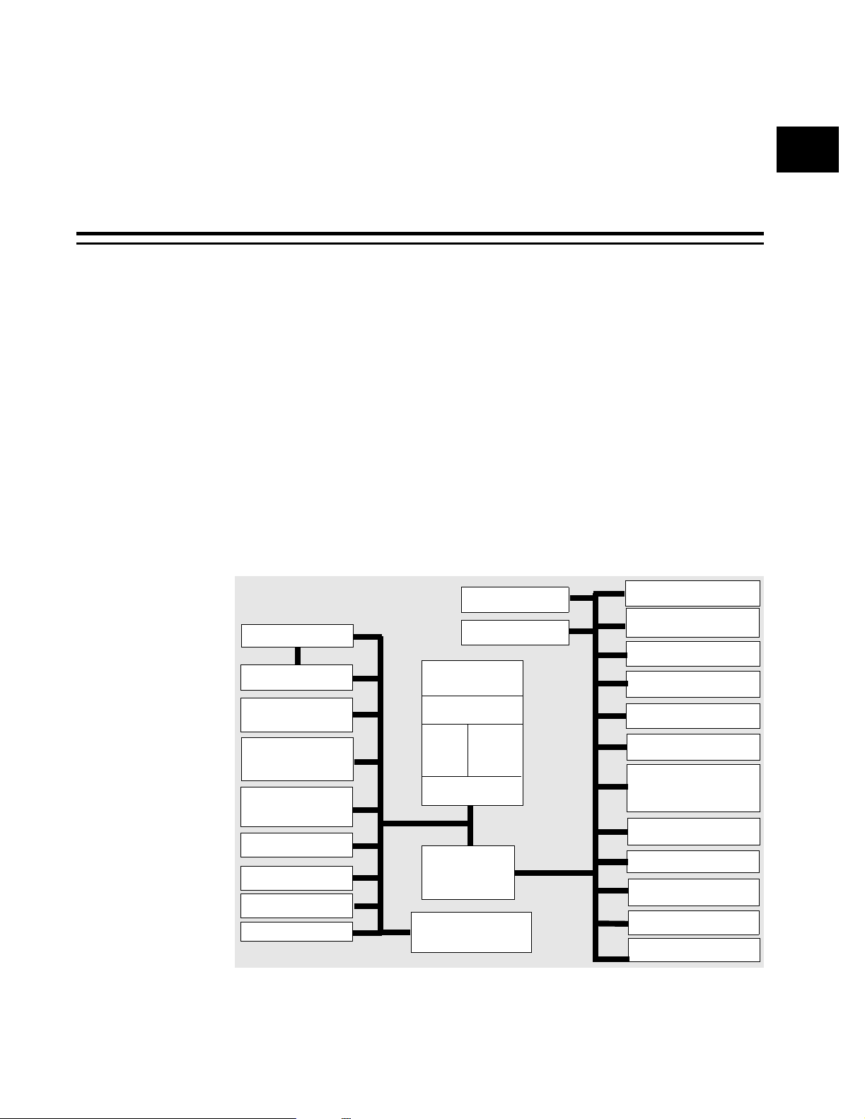
NN
)
C
1.1 Introduction
The EP93 12 is a highly integr ated system-on -chip processor th at paves the
way for a multitude of next-generation consumer and industrial electronic
products. De signers of digital m edia se rvers and jukebo xes, te lematic control
systems, thin client s, set-top boxes, point-of -sal e ter minals, industrial control s,
biometric security systems, and GPS devices will benefit f rom the EP93 12’s
integrated architecture and advanced features. In fact, with amazingly agile
performance provided by a 200 MHz ARM920T processor, and featuring an
incredibly wide breadth of perip heral interface s, the EP9312 is well suited to
an even bro ade r rang e of hig h volu me a pp licatio ns. Furthe rmo re, by enab ling
or disabling the EP9312’s peripheral interfaces, designers can reduce
development costs and accelerate time-to-market by creating a single platform
that can be easily mod if ied to deliver a v ariety of differe nt iated end p roducts.
Figure 1-1. EP9312 Block Diagram
Chapter 1
1Introduction
1
18-bit Raster LCD
SDRAM
SRAM/
FLASH/ROM
12 Channel DMA
Engine
1/10/100 Ethernet
MAC
JTAG
USB Host, 3 Ports
IDE
Boot ROM
UART1 w/ HDLC
UART3 w/ HDLC
MaverickCrunch
Coprocessor
ARM920T
I-Cache
AMBA High-Speed Bus (AHB)
Vectored Interrupt
Controllers (2)
D-Cache
16KB
AHB/APB
16KB
MMU
Bridge
UART2 w/ IrDA
System Ctrl - PLLs (2
Touch Screen AD
TM
8x8 Key Scan
PWM
2
S (IIS)
I
AMBA Peripheral Bu s (APB)
Enhanced GPIO
EEPROM, LED (2)
SPI
AC’97
RTC with Trim
Watchdog Timer
Timers
EP9312 User’s Manual - DS515UM2 27
Copyright 2004 Cirrus Logi c
Page 28

Introduction
1 1.2 EP9312 Features
The EP9312 system-on-chip processor has the following features:
• 200 MHz ARM920T Processor
• 16 KByte data cache and 16 KByte instruction cache
• MMU enabling Linux
• 100 MHz system bus
• MaverickCrunch
• Floating point, intege r and signal p roc essing ins tr uc t ions
• Optimized for digital music compression algorith ms
• Hardwar e interlocks allow in-lin e c oding
• MaverickKey
• 32-bit unique ID
• 128-bit random ID
• Integrated Peripheral Interfa c es
• EIDE, up to 2 devices
• 1/10/10 0 M bps Et hernet MAC
• Three-port USB 2.0 Full Speed host (OHCI)
™
™
IDs for Digital Rights Management or Design IP Security
®
and Windows® CE
Coprocessor
–
• Three UA RTs (16550 Type)
• IrDA interface, slow and fast mode
• LCD interface
• Touch screen interface
•SPI port
• AC ‘97 inte rf ac e
• I2S interface, up to 6 channels
• 8x8 keypad scanner
• External Memory Options
• 32-bit SDRAM interface, up to four banks
• 32/16/8-bit SRAM/Flash/ROM interface (I/F)
• Serial EE PR OM interfa c e
• Internal P eripherals
• Real-Time clock with software trim
28 EP9312 User’s Manual - DS515UM2
Copyright 2004 Cirrus Logic
Page 29

Introduction
NN
• 12 DMA channels for data transfer that maximizes syste m
performance
•Boot ROM
• Dual PLLs c ont rol all clock dom ains
• Watchdog timer
• Two general purpose 16-bit timers
• General pu rpose 32-bit t im er
• 40-bit debug timer
• General-Purpose I/Os
• 16 enhanced GPIOs inc luding inte rrupt capability
• 31 additional optional GPIOs multiplexed on peripherals
• Available in 352-pin PBGA package
1.3 EP9312 Applications
The EP9312 can be used in a variety of applications, such as:
• Digital media servers
1
• Integrated home media gateways
• Digital audi o juk eboxes
• Portable audio/video players
• Streaming audio / v ideo players
• Telematic control syste ms
• Set-top boxes
• Point-of-sale terminals
• Thin clients
• Internet T Vs
• Biometric security systems
• Industrial controls
• GPS & fleet management systems
• Educational toys
• Voting machines
• Medical e quipment
EP9312 User’s Manual - DS515UM2 29
Copyright 2004 Cirrus Logi c
Page 30

Introduction
1 1.4 Overview of EP9312 Features
1.4.1 High-Performance ARM920T Processor Core
The EP9312 features an advanced ARM920T processor design with an MMU
that supports Linux®, Windows® CE, and many other embedded operating
systems . T he ARM920T’s 32-bit m ic rocontroller arch ite c tu re, with a f iv e-stage
pipeline , del ivers impr ess ive perfo rma nce at ve ry lo w po wer. The in clud ed 16
KByte instruction cache and 16 KByte data cache provide zero-cycle latency
to the cu rrent pr ogram and d ata, or c an be lo cked to pro vide gu arantee d nolatency access to critical instructions and data. For applications with
instruction memory size restrictions, the ARM920T’s compressed Thumb
instruction set provides a space-efficient design that maximizes external
instruction memory usage.
1.4.2 MaverickCrunch™ Coprocessor for Ultra-Fast Math Processing
The MaverickCrunch coprocessor is an advanced, mixed-mode math
coprocessor that greatly accelerates the single and double-precision integer
and floating-point processing capabilities of the ARM920T processor core.
The engi ne simplifies th e end-user ’s programmin g task by using predefin ed
coprocessor instructions, by utilizing standard ARM compiler tools, and by
requiring just one debugger session for the entire system. Furthermore, the
integrate d design provides a single instructio n stream and the ad vantage of
zero latency for cached instructions. To emulate this capability, competitors’
solutions add a DSP to the system, which requires separate
compiler /l ink er/debug ger tool sets. Th is additional D SP requires program m ers
to write two separate programs and debug them simultaneously, which can
result in frus t ration and cos t ly delays.
®
The single-cycle integer multiply-accumulate instruction in the
MaverickCrunch coprocessor allows the EP9312 to offer unique speed and
performa nce whi le enco ding d igital aud io and v ideo f ormats, pr ocessin g data
via Ethernet, and performing other math-intensive computing and dataprocessing functio ns in c onsumer and industrial electronics.
1.4.3 MaverickKey™ Unique I D Secures Di gital Content and OEM Designs
Maverick Key uni que hardw are prog ramm ed IDs pro vide an ex cellen t solution
to the growing concern over secure Web content and commerce. With Internet
security playing an important role in the delivery of digital media such as books
or music, traditiona l software method s are quickly beco ming unreliable. T he
MaverickKey unique IDs provide OEMs with a method of utilizing specific
hardware IDs for DRM (D igital Rights Ma nagemen t) me c hanisms.
30 EP9312 User’s Manual - DS515UM2
Copyright 2004 Cirrus Logic
Page 31

Introduction
NN
MaverickKey uses a specific 32-bit ID and a 128-bit random ID that are
programmed into the EP9312 through the use of laser probing technology.
These IDs can then be used to match secure copyrighted content with the ID
of the target device that the EP9312 is powering, and then deliver the
copyrighted information over a secure connection. In addition, secure
transactions can benefit by matching d evice IDs to server IDs.
MaverickKey IDs can also be used by OEMs and design houses to protect
against design piracy by presetting ranges for unique IDs. For more
information on securing your design using MaverickKey, please contact your
Cirrus Log ic s ales representative.
1.4.4 Integrated Three-port USB 2.0 Full Speed Host with Transceivers
The EP931 2 integrat es three US B 2.0 Full Speed host po rts. Fully comp liant
to the OHCI USB 2.0 Full Speed specification (12 Mbps), the host ports can be
used to provide connections to a number of external devices including mass
storage d evice s, ext erna l po rtable d evice s su ch as au dio play ers o r came ras,
printers, or USB hubs. Naturally, the three-port USB host also supports the
USB 2.0 L ow Speed standa rd. This provide s the oppo rtunity t o create a wide
array of flexible system configurations.
1.4.5 Integrated Ethernet MAC Reduces BOM Costs
1
The EP9312 integrates a 1/10/100 Mbps Ethernet Media Access Controller
(MAC) on the device. With a simple connection to an MII-based external PHY,
an EP9312-based system has easy, high-performance, cost-effective Internet
capability.
1.4.6 8x8 Keypad Interface Reduces BOM Costs
The keypad circuitry scans an 8x8 array of 64 normally open, single pole
switches. Any one o r two keys d epressed w ill be de-boun ced and dec oded.
An interrupt is generated whenever a stable set of depressed keys is detected.
If the k eypad is not utilize d, t he 1 6 colum n/row pi ns m a y b e us ed a s ge ne ralpurpose I /O s .
1.4.7 Multiple Booting Mechanisms Increase Flexibility
The processor includes a 16 KByte boot ROM to set up standard
configurations. Optionally, the processor may be booted from FLASH memory,
over the SPI serial interface, or through the UART. This boot flexibility makes it
easy to design user-controlled, field-upgrad able systems. See Chapter 4 on
page 119, for additi onal details.
EP9312 User’s Manual - DS515UM2 31
Copyright 2004 Cirrus Logi c
Page 32

Introduction
1
1.4.8 Abundant General Purpose I/Os Build Flexible Systems
The EP93 12 includes both enha nced and sta ndard gene ral-purpo se I/O pins
(GPIOs) . The 16 differ ent e nhanc ed G PIOs ma y ind ividu ally b e con figu red as
inputs, outputs, or interrupt-enabled inputs. There are an additional 31
standard GPIOs that may individually be used as inputs, outputs, or opendrain pin s. T he s tanda rd G PIOs are mu ltiple xed wit h pe riph eral func tion pins ,
so the nu mber available de pends on the u tilizatio n of peripherals. Toge ther,
the enhanced and standard GPIOs facilitate easy system design with external
peripher als not integrat ed on the EP 9312.
1.4.9 General-Purpose Memory Interface (SDRAM, SRAM, ROM and FLASH)
The EP9 312 feature s a unified m emory addre ss model in which all memory
devices a re access ed over a common address/d ata bus. A sepa rate inte rnal
bus is ded ic at ed to the read-only R as t er/ D is play refres h engine, w hile the rest
of the memory accesses are performed via the high-speed processor bus. The
SRAM memory controller supports 8, 16 and 32-bit devices and
accommodates an internal boot ROM concurrently with a 32-bit SDRAM
memory.
1.4.10 12-Bit Analog-to-Digital Converter (ADC) Provides an Integrated
Touch-Screen Interf ace or General ADC Functionality
The EP9312 includes a 12-bit ADC, which can be utilized either as a touchscreen inter face or for general ADC functionalit y. The touch-screen int erface
performs all sampling, averaging, ADC range checking, and control for a wide
variety of ana log-re sis tive to uchsc reen s. To improve system perfor man ce, the
controller only interrupts the processor when a meaningful change occurs.
The touch -sc reen har dwa re m ay b e di sab led, a nd t he s witch ma trix an d A DC
controlle d directly for general AD C us age if desired.
32 EP9312 User’s Manual - DS515UM2
Copyright 2004 Cirrus Logic
Page 33

Chapter 2
OO
2ARM920T Core and Advanced High-Sp eed Bus (AHB)
2.1 Introduction
This section discus s es t he ARM920T proces s or core an d t he Advan c ed HighSpeed Bus (AHB ).
2.2 Overview: ARM920T Processor Core
The ARM920T is a Harvard architecture processor core with separate
16 kb yte instruction and data caches wit h an 8-word line l ength used in the
EP9312 . The process or core utilize s a five-stage pip eline consis ting of fetch,
decode, execute, data memory acces s , and write stages.
2.2.1 Features
Key fea t ures include:
• ARM V4T (32-bit) an d T humb (16-b it co m pressed) ins t ruction sets
• 32-bit Adv anced Micr o-C ontrolle r Bus Archite c tu re (AMBA)
2
• 16 kbyte Instructio n Cache with lockdown
• 16 kbyte Data Cache (programmable write-through or write-back) with
lockdown
• Write Buffer
• MMU for Microsoft Windows CE and Linux operating systems
• Translation Look-aside Buffers (TLB) with 64 Data and 64 Instruction
Entries
• Programmable Page Sizes of 64 kbyte, 4 kbyte, and 1 kbyte
• Independent lockd ow n of TLB Ent ries
• JTAG Interface for Debug Control
• Coprocessor Interface
EP9312 User’s Manual - DS515UM2 33
Copyright 2004 Cirrus Logi c
Page 34

2
ARM920T Core and Advanced High-Speed Bus (AHB)
2.2.2 Block Diagram
Figure 2-1. ARM920T Block Diagram
External
Co-Proc
Interface
JTAG
Instruction
cache
R13
ARM9TDMI
Processor core
(Integral
EmbeddedICE)
R13
Data cache Data MMU
Instruction
MMU
CP15
Write
Buffer
Write Back
PA TAG
RAM
AMBA
Bus
Int.
APB
2.2.3 Operations
The ARM920T core follows a Harvard architecture and consists of an
ARM9TD MI core, MMU , instruction and data ca che. The core supports both
the 32-bit AR M and 16-bit Thumb inst ruc t ion sets.
The inte rnal bus struct ure (AMBA) i ncludes both an internal hi gh speed and
external low speed bus. The high speed bus AHB (Advanced Highperformance Bus) contains a high speed internal bus clock to synchronize
coprocessor, MMU, cache, DMA controller, and memory modules. AMBA
includes a AHB/APB bridge to the lower speed APB (Advanced Peripheral
Bus). The APB bus connects to lower speed peripheral devices such as
UARTs a nd GPIOs.
The MMU provides memory address translation for all memory and
peripherals designed to remap memory devices and peripheral address
locations. Sections, large, small and tiny pages are programmable to map
memory in 1 Mbyte, 64 kbyte, 4 kbyte, 1 kbyte size blocks. To increase syst em
34 EP9312 User’s Manual - DS515UM2
Copyright 2004 Cirrus Logic
Page 35

ARM920T Core and Advanced High-Speed Bus (AHB)
performance, a 64-entry translation look-aside buffer will cache 64 address
locations before a TLB miss occurs.
OO
A 16 kbyte instruction and a 16 kbyte data cache are included to increase
performance for cache-enabled memory regions. The 64-way associative
cache a lso has l ock-do wn capab ility. Cached ins tructio ns and data also have
access to a 16 -word data an d 4-word instr uction write bu ffer to allow cach ed
instructions to be fetched and decoded while the write buffer sends the
information to the ex te rnal bus.
The ARM920T core supports a number of coprocessors, including the
MaverickCrunch coprocessor by means of a specific pipeline architecture
interface.
2.2.3.1 ARM9TDMI Core
ARM9TDMI core is responsible for executing both 32-bit ARM and 16-bit
Thumb instructions. Each provides a unique advantage to a system design.
Internally, the instructions enter a 5-stage pipeline. These stages are:
• Instruction Fetch
• Instruction Decode
• Execute
• Data Memory Access
• Register Wr ite
2
All instruct ions are fully interlocke d. This mec hanism will d elay the exec ution
stage of a instruction if data in that instruction comes from a previous
instruction that is not available yet. This simply insures that software will
function identically across different implementations.
For memor y ac cess instru ctio ns, th e bas e regis te r used for the acces s will be
restored by the processor in the event of an Abort exception. The base
register will be restored to the v alue contained in th e processor regis t er before
exec ut ion of the instruction.
The ARM9TDMI core memory interface includes a separate instruction and
data interfac e to allow concurr ent access of inst ructions and data t o reduce
the number of CPI (cycles per instruction). Both interfaces use pipeline
addressing. The core can operate in big and little endian mode. End ianess
affects both the address and the data int erf ac es.
The memory interface executes four types of memory transfers: sequential,
non-sequential, internal, and coprocessor. It will also support uni- and bidirection al t ransfer mo des.
The core provides a debug interface called JTAG (Joint Testing Action Group).
This interf ac e provides debug capa bility with five ex t ernal control signals:
EP9312 User’s Manual - DS515UM2 35
Copyright 2004 Cirrus Logi c
Page 36

ARM920T Core and Advanced High-Speed Bus (AHB)
• TDO - Test Data Out
• TDI - Test Data In
2
• TMS - Test Mode Select
• TCK - Test Clo c k
• nTRST - Test Reset
There are s ix scan chains (0 through 5) in th e ARM9TDMI controlled by the
JTAG Test Access Port (TAP) controller. Details on the individual scan chain
function and bit order can be found in the ARM920T Technical Reference
Manual.
2.2.3.2 Memory Management Unit
The MMU provides the translation and access permissions for the address
and data ports for the ARM9TDMI core. The MMU is controlled by page tables
stored in system memory and accessed using the CP15 register 1. The main
features of t he M M U are as follow s:
• Address Translation
• Access P erm issions an d D omains
• MMU Cache and Write Buffer Access
2.2.3.2.1 Address Translation
The virtual address from the ARM920T core is modified by R13 internally to
create a modified virtual address. The MMU then translates the modified
virtual address from R13 by the CP15 register 3 into a physical address to
access external memory or a device. The MMU loo ks for the physical address
from the Translati on Table Base (TTB ) in system memory. It will also update
the TLB cac he.
The TLB is two 64-entry caches, one for data and one for in struction. If the
physical address f or the current virtu al address is not found in the TLB (miss ),
the processor will go to external memory and look for the TTB in system
memory. The internal translation table walks hardware steps through the page
table setup in external memory for the appropriate physical address.
When the physical address is acquired, the TLB is updated. When the address
is found in the TLB, system performance will increase since it will take
additional cycles to access memory and update the TLB.
Translation of system memory is done by breaking up the memory into
different si ze bl ocks cal l ed sect i ons, l arg e pa ges, sma l l p ages, an d t iny p a ges.
System memory and registers can be remapped by the MMU. The block sizes
are as follo w s :
• Section - 1 Mbyte
36 EP9312 User’s Manual - DS515UM2
Copyright 2004 Cirrus Logic
Page 37

• Large Pa ge - 64 kby t e
• Small Page - 16 kbyte
ARM920T Core and Advanced High-Speed Bus (AHB)
OO
• Tiny Page - 1 kbyte
2.2.3.2.2 Access Permission and Domains
Access to any s ection or page of memory is dep endent on its do main. The
page table in exte rnal memory als o contains access permissions fo r all subdivisions of e xternal memory. Access to specific instructions or data h as three
possible states, assuming access is permitted:
• Client: Access permissions based on the section or page table descriptor
• Manager: Ignore access permissions in the section or page table
descriptor
• No access: any attempted access generates a domain fault
2.2.3.2.3 MMU Enable
Enabling the MMU all ows for system mem ory control, but is also r equired if
the data cache and the write buffer are to be used. These features are
enabled for specific memory regions, as defined in the system page table.
MMU enable is done via C P15 register 1. The proc edure is as fol low s :
1. Program the Translation Table Base (TTB) and domain access control
registers.
2
2. Create level 1 and level 2 pages for the system and enable the cache and
the write buffer.
3. Enab le M M U - bit 0 of CP15 register 1.
2.2.3.3 Cache and Write Buffer
Cache configuration is 64-way set associative. There is a separate 16 kbyte
instruction and data cache. The cache has the following characteristics:
• 8 words per lin e with 1 val id bit a nd 2 di rty bi ts per line for al lowing halfline write- backs.
• Write-through and write-back capable, selectable per memory region
defined by th e M M U .
• Pseudo random or round robin replacement alg orit hms for c ac he miss es .
This is determi ned by the R R bit (bit 14 in CP15 register 1). An 8-word line
is reloaded on a cache m is s .
• Independent cache lock-down with granularity of 1/64th of total cache
size or 256 bytes for both instructions and data. Lock-down of the cache
will prevent an eight-word cache line fill of that region of cache.
• For compatibility with Windows CE and to reduce latency, physical
EP9312 User’s Manual - DS515UM2 37
Copyright 2004 Cirrus Logi c
Page 38

2
ARM920T Core and Advanced High-Speed Bus (AHB)
address es stored for data c ac he entries are stored in th e PA TAG RAM to
be used fo r cache line write-b ack operations with out need of the MMU ,
which pre v ent s a pos s ible TLB mis s th at w ould degrade performance.
• Write Buffer is a 4-word instruction x 16-word data buffer. If enabled,
writes are s ent to b uffer dire ctly f rom cach e o r from t he C PU in the eve nt
of a cache m is s or c ac he not ena bled.
2.2.3.3.1 Instruction Cache Enable
• At reset, the cache is di sa bled.
• A write to CP15 register 1, bit 12, will enable or disable the Instruction
Cache. If the Instruction Cache (I-Cache) is enabled without the MMU
enabled , a ll ac c es s es are treat ed as cachea ble.
• If disabled, current contents are ignored. If re-enabled before a reset,
contents will be unchange d but m ay not be c oherent with main memory. If
so, contents must be flushed before re-enabling.
2.2.3.3.2 Data Cache Enable
• A write to CP15 register 1, bit 0, will enable or disable the Data Cache (DCache)/Write Buffer.
• D-Cache must only be enabled when the MMU is enabled. All data
accesses are subject to MMU and permission che cks.
• If disabled, current contents are ignored. If re-enabled before a reset,
contents will be unchanged but may not be coherent with main memory.
Depending on system software, a clean and invalidate action may be
requ ired before re- enabling.
2.2.3.3.3 Write Buffer Enable
• The Write b ugger is enabled by the page table ent ries in the MMU. T he
Write buffer is not enabled unless MMU is enabled .
2.2.4 Coprocessor Interface
The MaverickCrunch coprocessor is explained in detail in Chapter 3. The
relations hip between the ARM coprocessor ins tructions and Ma verickCrunch
coproce s so r is als o explaine d in Chapter 3.
The ARM c oprocesso r ins t ruction se t in cl udes the follo w ing:
• LDC - Load co processo r fr om m emory
• STC - Store coprocessor regis t er from memory
• MRC - Move to ARM register from coprocessor register
• MCR - Move to coprocessor register fr om ARM register
38 EP9312 User’s Manual - DS515UM2
Copyright 2004 Cirrus Logic
Page 39

ARM920T Core and Advanced High-Speed Bus (AHB)
• Access to sixteen (C0 through C15) 64-bit registers to access the
coproce ssor for d ata transfer and da ta manipulat ion to b e used wi th the
above instructions. See Chapter 3, Section 3.2 on page 73 for a code
example.
2.2.5 AMBA AHB Bus Interface Overview
The AMBA AHB is designed for use with high-performance, high clock
frequency system modules. The AHB acts as the high-performance system
backbon e bus. AHB su pports the efficie nt connection of processo rs, on-chip
memorie s and off-chip e xternal m emory inte rfaces with low-pow er periphera l
functions. AHB is also specified to ensure ease of use in an efficient design
flow using synthesis and automated test techniques. Figure 2-2 shows a
typical AM BA AHB Sys t em .
AHB (Advanced High-Performance Bus) connects with devices that require
greater bandwidth, such as DMA controllers, external system memory, and
coprocessors. The AMBA AHB bus has the following characteristics:
OO
2
• Burst Transactions
• Split Transactions
• Bus Mast er hand-ove r t o devices, th at is , DSP or DMA c ont roller
• Single cloc k edge operat ions
APB (Advanced Peripheral Bus) is a lower bandwidth lower power bus which
provides the following:
• Low Power Operations
• Latched address and control
• Simple Interface
Figure 2-2. Typical AMBA AHB System
External
Memory
Inte r fac e
ARM9TDMI
Co-
Processo
USB
r
AHB APB
DMA
Controller
AHB/
APB
B
r
i
d
g
e
UART SPI
GPIO
AC97
EP9312 User’s Manual - DS515UM2 39
Copyright 2004 Cirrus Logi c
Page 40

2
ARM920T Core and Advanced High-Speed Bus (AHB)
2.2.6 EP9312 AHB Implementation Details
Periphe rals that ha ve high ban dwidth or late ncy requirem ents are c onnected
to the EP9312 processor using the AHB bus. These include the external
memory interface, Vectored Interrupt Controllers (VIC1, VIC2), DMA,
LCD/Raster registers, USB host, IDE, Ethernet MAC and the bridge to the
APB interf ace. The AHB/A PB Bridge transpare ntly converts the AH B access
into the slower sp eed APB ac cesses. All of the c ontrol re gisters for t he APB
peripherals are programmed using the AHB/APB bridge interface. The main
AHB data and address lines are configured using a multiplexed bus. This
removes t he need for three s tate buffers and bus hold ers and simplif ies bus
arbitration. Figure 2-3 shows the main data paths in the EP9312 AHB
implementation.
Figure 2-3. EP9312 Main Data Paths
VIC2
VIC1
Ethernet
ARM920T
18 Bit Raster
LCD I/ F
SDRAM
Controller
E
B
I
Static
Memory
Controller
IDE
USB
Host
AHB
Maverick
Crunch
Boot ROM
DMA
UARTs
Timers
AHB/APB
bridge
RTC
Watchdog
Test
Support
APB
Touchscreen
8x8 Key Mtx
GPIOs
PWM
SPI
I2S
IrDA
PLL1 PLL2
Clock & State
Control
AC97
40 EP9312 User’s Manual - DS515UM2
Copyright 2004 Cirrus Logic
Page 41

ARM920T Core and Advanced High-Speed Bus (AHB)
Before an AMBA-to-AHB transfer can commence, the bus master must be
granted ac cess to th e bus. This pro cess is star ted by the ma ster asser ting a
requ es t signal to t he arbiter. Then the arbiter i ndicates when the master will be
gran t ed use of the bus. A granted bus master starts an AMBA-to- AH B transfer
by drivin g the ad dress and contr ol signa ls. These signals provid e inform ation
on the address, direction and width of the transfer, as well as indicating
whether th e tr ansfer forms part of a burst.
Two different forms of burst transf ers are allowed:
• Incrementing bursts, w hic h do not wrap at address boundaries
• Wrapping bursts, which w rap at particul ar address boundaries .
A write data bus is us ed to move da ta from the mast er t o a s lav e, while a read
data bus is used to move data from a slave to the master. Every transfer
consists of:
• An address and control cycle
• One or more cycles for the data.
OO
2
In normal operation a master is allowed to complete all the transfers in a
particular burst before the arbiter grants another master access to the bus.
However, in orde r t o av oid exces s iv e arbitration latencies, it is pos s ible for the
arbiter to break up a bu rst , and , i n such cases, th e master must re - arbitr a te for
the bus in order to complete the remaining transfers in the burst.
2.2.7 Memory and Bus Access Errors
There are several possible sources of access errors.
• Reads to reserved or undefined register memory addresses will return
indeterm inate data. Writes to re served or undefin ed memory addre sses
are gene rally ig nored, but this behav ior is no t guara nteed. M any re gister
addresses are not fully decoded, so aliasing may occur. A ddresses and
memory ranges listed as Reserved should not be accessed; access
behavior to these regions is not defined.
• Access to non-exist ent register s or m em ory may re s ult in a bus error.
• Any acce ss in the APB co ntrol regi ster space w ill com plete norm ally, as
thes e devices have no mea ns of sign aling an error.
• Access to non-existent AHB/APB registers may result in a bus error,
dependi ng on the de vice and nat ure of the erro r. Devic e specific ac cess
rules are def ined in the d ev ic e descripti ons.
• External memory access is controlled by the Static Memory Controller
(SMC) and the Synchronous Dynamic RAM (SDRAM) controller. In
general, a ccess to non-exis tent externa l memor y will comp lete norm ally,
with reads returning random false data.
EP9312 User’s Manual - DS515UM2 41
Copyright 2004 Cirrus Logi c
Page 42

2
ARM920T Core and Advanced High-Speed Bus (AHB)
2.2.8 Bus Arbitration
The arbitration mechanism is used to ensure that only one master has access
to the bus it controls at any one time. The arbiter performs this function by
observing a number of different requests to use the bus and deciding which is
currently t he highest priority mast er requesting the bus.
The arbitration scheme can be broken down into three main areas:
• The main AHB system bus arbiter
• The SDRAM slave interface arbiter
• The EBI bus arbiter
2.2.8.1 Main AHB Bus Arbiter
This arb it er controls t he bus master arbitration f or the A H B bus. Th e AHB b us
has eight Ma s te r interfaces, t hes e are:
• ARM920T
• DMA controller
• USB host (USB1, 2, 3)
• Ethernet MAC
• LCD/Raster and Raster Hardware Cursor.
These inte rfac es ha ve an order of priori ty tha t is lin ked clo sely with t he pow er
saving mod es. The po wer saving m ode s of H alt an d Standby force t he arbit er
to grant the default bus master, in this case, the ARM920T.
In summa ry, the order of priority of the bus m aste rs, from highe st to lowes t, is
shown in Table 2-1.
T able 2-1: AHB Arbiter Priority Scheme
Priority
Number
1 Raster Cursor Raster Raster Raster
2 MAC Raster Cursor Raster Cursor DMA
3 USB MAC DMA MAC
4 DMA USB USB USB
5 ARM920T ARM920T MAC Raster Cursor
6 Raster DMA ARM920T ARM920T
PRIORITY 00
(Reset value)
PRIORITY 01 PRIORITY 10 PRIORITY 11
The priority of the Arbiter can be programmed in the BusMstrArb register in
the Clock and State Controller. The Arbiter can also be programmed to
degrant one of the following master s : DMA, USB Host o r Etherne t MAC, if an
interrupt (IRQ or FIQ) is pending or being serviced. This prevents one of these
masters fr om blocking important int errupt s erv ic e routine s . These mas t ers are
42 EP9312 User’s Manual - DS515UM2
Copyright 2004 Cirrus Logic
Page 43

prevente d from acces sing the bus , and their bus requests are masked, un til
the IRQ/FIQ is removed (by the Interrupt Service Routine), at which point their
bus requests will be recognized. The default is to program the Arbiter so that it
does not degrant any of thes e m asters.
In norma l operat ion, whe n the AR M920 T is gran ted th e bus an d a requ est to
enter H alt mode is received, the ARM 920T is d e-granted from the AHB bus .
Any othe r master request ing the bus in Ha lt mode (accordin g to the priority )
will be granted the bus. In the case of the entry into Standby, the dummy
master will be granted the bus, which simply performs IDLE transfers. In this
way, all the masters except the ARM920T can be used during Halt mode, but
are shutdown during an entry into Standby.
2.2.8.2 SDRAM Slave Arbiter
The SDR AM controller ha s a slave inter face fo r the main AHB bus and the
Raster controller DMA bus. In order to control the accesses to these memory
systems, the SDRAM controller has an arbiter that prioritizes between the
AHB and t he Rast er DMA bu s. In th is case the Raster contro ller bus is given
priority. If an access from the AHB is requested at the same tim e as a Raster
DMA, the Ra s te r w ill be given acc ess while the AHB requ es t is queued.
ARM920T Core and Advanced High-Speed Bus (AHB)
OO
2
2.2.8.3 EBI Bus Arbiter
This arbiter is used to arbitrat e bet wee n acces ses f rom the SD RA M cont rolle r
and the Static Mem ory controller. The prio rity is given to acc esses from the
SDRAM controller.
2.3 AHB Decoder
The AHB decoder contains the memory map for all the AHB masters/slaves
and the APB bridge. When a particular address range is selected, the
appropr iat e s ignal is gene rated. It is de fin ed in Tab le 2-2.
(For additional information, see “Reference Documents”, on Page 4.)
EP9312 User’s Manual - DS515UM2 43
Copyright 2004 Cirrus Logi c
Page 44

2
ARM920T Core and Advanced High-Speed Bus (AHB)
Table 2-2: AHB Peripher al Address Range
Address Range Register Width Peripheral Type Peripheral
0x800D_0000 - 0x800F_FFFF - - Reserved
0x800C_0000 - 0x800C_FFFF 32 AHB VIC2
0x800 B_0 000 - 0x800 B_FFFF 32 AH B VIC1
0x800 A_0 000 - 0x800 A_FFFF 32 AH B IDE
0x80 09 _0 000 - 0x800 9_ FFFF 3 2 AHB
0x8008_0000 - 0x8008_FFFF 32 AHB SRAM Controller
0x80 07 _0 000 - 0x800 7_ FF F F - - Reser ve d
0x8006_0000 - 0x8006_FFFF 32 AHB SDRAM Controller
0x80 05 _0 000 - 0x800 5_ FF F F - - Reser ve d
0x80 04 _0 000 - 0x800 4_ FF F F - - Reser ve d
0x8003_0000 - 0x8003_FFFF 32 AHB Raster
0x8002_0000 - 0x8002_FFFF 32 AHB USB Host
0x8001_0000 - 0x8001_FFFF 32 AHB Ethernet MAC
0x80 00 _0 000 - 0x800 0_ FFFF 3 2 AHB DMA
Note: Due to decoding optimization, the AHB peripheral registers are aliased
throughout each peripherals register bank. Do not program access to an
unspecified register within the bank.
Boot ROM physical
address
2.3.1 AHB Bus Slave
An AHB slave responds to transfers initiated by bus masters within the
system. The slave uses signals from the decoder to determine when it should
respond to a bus transfer. All ot her signa ls require d for the transfer, such as
the addres s and control informatio n, are generat ed by the bus master.
2.3.2 AHB to APB Bridge
The AH B to AP B bridge is an AHB s lave, pr oviding an in terface between the
high-speed AHB and the low-power APB. Read and write transfers on the
AHB are co nverted into equivale nt transfers on the A PB. As the APB is not
pipelined. Wait states are added during transfers to and from the APB when
the AHB is required to wa it fo r th e APB.
The main se c tio ns of t his m odule are:
• AHB slave bus interfa c e
• APB transfer state machine, which is independent of the device memory
map
• APB output signal generation.
44 EP9312 User’s Manual - DS515UM2
Copyright 2004 Cirrus Logic
Page 45

ARM920T Core and Advanced High-Speed Bus (AHB)
2.3.2.1 Function and Operation of APB Bridge
The APB bridge responds to transaction requests from the currently granted
AHB master. The AHB transactions are then converted into APB transactions.
If an undefined location is accessed, operation of the system continues as
normal, but no peripherals are selected. The APB bridge acts as the only
master on the APB.
The APB memory map is shown in Table 2-3.
T able 2-3: APB Peripheral Address Range
OO
2
Address Range
0x8095_0000 - 0x9000_FFFF - - Reserved
0x8094_0000 - 0x 8094_FFFF 16 APB Wa tchdog Timer
0x8093_0000 - 0x8093_FFFF 32 APB Syscon
0x8092_0000 - 0x8092_FFFF 32 APB Real tim e clock
0x8091_0000 - 0x8091_FFFF 16 APB Pulse Width Modulation
0x8090_0000 - 0x8090_FFFF 32 APB Touchscreen
0x808F_0000 - 0x808F_FFFF 16 APB Key Matrix
0x808E_0000 - 0x808E_FFFF 32 APB UART3
0x808D_0000 - 0x808D_FFFF 8 APB UART2
0x808C_0000 - 0x808C_FFFF 32 APB UART1
0x808B_0000 - 0x808B_FFFF 32 APB IrDA
0x808A_0000 - 0x808A_FFFF 16 APB SPI
0x8089_0000 - 0x8089_FFFF - - Reserved
0x8088_0000 - 0x 8088_FFFF 32 APB AAC
0x8087_0000 - 0x8087_FFFF - - Reserved
0x8086_0000 - 0x8086_FFFF - - Reserved
0x8085_0000 - 0x8085_FFFF - - Reserved
0x8084_0000 - 0x 8084_FFFF 16 APB GPIO
0x8083_0000 - 0x8083_FFFF 32 APB Security
0x8082_0000 - 0x 8082_FFFF 32 APB I2S
0x8081_0000 - 0x 8081_FFFF 32 APB Ti mers
0x8080_0000 - 0x8080_FFFF - - Reserved
0x8010_0000 - 0x807F_FFFF - - Reserved
Register
Width
Peripheral
Type
Peripheral
Note: Due to decoding optimization, the APB peripheral registers are aliased
throughout each peripherals register bank. Do not program access to an
unspecified register within the bank.
2.3.3 APB Bus Slave
An APB slave responds to transfers initiated by bus masters within the
system. The slave uses signals from the decoder to determine when it should
respond to a bus transfer. All ot her signa ls require d for the transfer, such a s
the addres s and control informatio n, are generat ed by the APB bridge.
EP9312 User’s Manual - DS515UM2 45
Copyright 2004 Cirrus Logi c
Page 46

2
ARM920T Core and Advanced High-Speed Bus (AHB)
2.3.4 Register Definitions
ARM has thirty seven 32-bit internal registers, some are modal, some are
banked. If operating in Thumb mode, the processor must switch to ARM mode
before taking an exception. The return instruction will restore the processor to
Thumb state. Most tasks are execu ted out of User mode.
User: Unprivileged norma l operating mode
FIQ: Fas t int errupt (hig h priority) mo de w hen FIQ is a s se rt ed
IRQ: Interrupt request (normal) mode when IRQ is asserted
Supervisor: Software interrupt instruction (SWI) or reset will cause entry
into this mode
Abort: Memory ac c ess violation will caus e entry into this m ode
Undef: Undefined instructions
System: Privileged mode. Uses sam e regis t ers as user mode
Table 2-4 illustrates the use of all registers for the following ARM920T
operating modes. Each will bank or store a specific number of registers.
Banked register information is not shared between modes. FIQs bank the
fewest number of registers which increases performance.
46 EP9312 User’s Manual - DS515UM2
Copyright 2004 Cirrus Logic
Page 47

Table 2-4: Register Organization Summary
User System Supervisor Abort Undefined IRQ FIQ
r0 r0 r0 r0 r0 r0 r0
r1 r1 r1 r1 r1 r1 r1
r2 r2 r2 r2 r2 r2 r2
r3 r3 r3 r3 r3 r3 r3
r4 r4 r4 r4 r4 r4 r4
r5 r5 r5 r5 r5 r5 r5
r6 r6 r6 r6 r6 r6 r6
r7 r7 r7 r7 r7 r7 r7
r8 r8 r8 r8 r8 r8
r9 r9 r9 r9 r9 r9
r10 r10 r10 r10 r10 r10
r11 r11 r11 r11 r11 r11
r12 r12 r12 r12 r12 r12
r13(sp) r13
r14(lr) r14
r15(pc) pc pc pc pc pc p c
ARM920T Core and Advanced High-Speed Bus (AHB)
Priveledged Modes
Exception Modes
r8_fiq
r9_fiq
r10_fiq
r11_fiq
r12_fiq
r13_svc r13_abt r13_und r13_irq r13_fiq
r14_svc r14_abt r14_und r14_irq r14_fiq
OO
2
Thumb
state lo w
registers
Thumb
state high
registers
cpsr cpsr cpsr cpsr cpsr cpsr cpsr
spsr_svc spsr_abt spsr_und spsr_irq spsr_fiq
Note: Colored areas represent banked regist ers.
User mode in Thumb state generally limits access to r0-r7. There are six
inst ructions that allow ac c ess to the high registers. For these 6 exceptions, the
processor must revert to ARM state. These exceptions are:
• r0-r12: General purpos e read/writ e 32-bit regist ers
• r13 (sp): Stack Pointer
• r14 (lr): Link Register
• r15 (pc): Prog ram C ounter
• cpsr: Current Program Status Register (contains condition codes and
operating modes)
• spsr: Saved Program Status R egister (saves CPSR when exception
EP9312 User’s Manual - DS515UM2 47
Copyright 2004 Cirrus Logi c
Page 48

2
ARM920T Core and Advanced High-Speed Bus (AHB)
occurs)
The ARM920T core has 16 coprocessor registers for control ove r the core.
Updates t o the coprocess or registers ar e written using th e CP15 instruct ion.
Table 2-5 describes the CP15 ARM920T registers.
Table 2-5: CP15 ARM920T Register Description
Register Description
ID Code: (Read/Only) This register returns a 32-bit device code. ID Code data represents
the core type, revision, part number etc. Access to this register is done with the following
instruction:
0
1
MRC p15 0, Rd, c0 , c0 , 0
Cache Code: This will also return cache type, size and length of both I-Cache and D-
Cache, size, and associativity. This is accessed with:
MRC p15 0, Rd, c0 , c0 , 1
Control Register: (Read/Wri te) Use this register to enable MM U, instruction and data
cache, round ro bin replacement ‘RR’-bi t, system p rotection, ROM protection, clocking
mode. Read/Write Instructions:
MRC p15 , 0, Rd, c1, c 0, 0 - Read control re gister - value stored in Rd
MCR p15, 0, Rd, c1, c0, 0 - Write control register - value first loaded into Rd
Translation Base Table: (Read/Write) Thi s register contains the start address of the firs t
level translation table. Upper18 bits represent the pointer to table base. Lower 14 bits
2
3
4
5
6
7
8
should be 0 for a write, unpredictable if read.
MRC p15, 0, Rd, c2, c0, 0 - Read TTB
MCR p15, 0, Rd, c2, c0, 0 - Write TTB
Domain Access Control: (Read/Write) This register sp ec ifies pe rmi ssions f or all 16
domains.
MRC p15, 0, Rd, c3, c0, 0
MCR p15, 0, Rd, c3, c0, 0
Reserved: Do not access. Unpredictable behavior may result.
Fault Status: (Read/Write) This regist er indicates type of fault and doma in of last data
abort.
MRC p15, 0, Rd, c5, c0, 0 - read data FSR value
MCR p15, 0, Rd, c5, c0, 0 - write data FSR value
Fault Address: (Read/Wr ite) This regist er contains address of the last data access abort.
MRC p15, 0, Rd, c6, c0, 0 - read data FAR data
MCR p15, 0, Rd, c6, c0, 0 - write data FAR data
Cache Operation: (Write/Only) This register will configure or perform a clean (flush) of the
cache and write buffer when written to. An example:
MRC p 1 5, 0, Rd, c7, c7, 0 - Inva lidate I/D- c ache
MRC p 1 5, 0, Rd, c7, c5, 0 - Inva lidate I-Cache
TLB Operatio n: (Write/Only) This register can configure or clean (flu sh) when written to:
MRC p15, 0, Rd, c8, c7, 0 - Invalidate TLB
Cache Lockdown: (Read/Write) Prevents certain cache-line fills from being overwritten
9
(locked).
MRC p15, 0, Rd, c9, c0, 1- Write lockdown base pointer for D-Cache
MRC p15, 0, Rd, c9, c0, 1 - Write lockdown base pointer for I-Cache
48 EP9312 User’s Manual - DS515UM2
Copyright 2004 Cirrus Logic
Page 49

Table 2-5: CP15 ARM920T Register Description (Continued)
Register Description
ARM920T Core and Advanced High-Speed Bus (AHB)
OO
11,12,14
2.3.5 Memory Map
The overall memory map for the device is shown in Table 2-6.
If internal Boot Mode is selected and the register BootModeClr has been
written, the address range 0x00 00_0000 -> 0x0000_FFFF is occupied by the
internal Boot ROM until the internal Boot Code is completed and then the map
reverts back to either Synchronous or Asynchronous memory in this address
space.
NOTE: Some memory locations are listed as Reserved. These memory
location s shou ld not b e us ed. Re ad ing f rom these mem ory loc atio ns will yield
invalid data. Writing to these memory locations may cause unpredictable
results.
10
13
15
TLB Lockdown: (Read/Write) Prevents TLB entries from being erased during a table walk.
MRC p15 , 0, Rd, c10, c0, 1- Write lockdown base pointer for data TLB entry
MRC p15, 0, Rd, c10, c0, 1 - Write lockdown base pointer for instruction TLB entry
Reserved
FCSE PID Register: (Read/Write) Addresses by the ARM9TDMI core in a range from 0 to
32MB are translated by this register to A + FCSE*32MB and remapped. If turned off,
straight address map to the MMU result.
Test Register O nly: Reads or writ es will ca use unpredictable behavior.
2
T able 2-6: Global Memory Map for the Two Boot Modes
Address Range Sync Memory Boot Async Memory Boot
ASD0 Pin = 1 ASD0 Pi n = 0
0xF000_0000 - 0xFFFF_FFFF Async memory (nCS0) Sync memory (nSDCE3)
0xE000_0000 - 0xEFFF_FFFF Sync memory (nSDCE2) Sync memory (nSDCE2)
0xD000_0000 - 0xDFFF_FFFF Sync memory (nSDCE1) Sync m emory (nSDCE1)
0xC000_0000 - 0xCFFF_FFFF Sync memory (nSDCE0) Sync m emory (nSDCE0)
0x9000_0000 - 0xBFFF_FFFF Not Used Not Us ed
0x8080_0000 - 0x8FFF_FFFF APB ma pped registers APB mapped registers
0x80 10 _0 000 - 0x807 F_ FF F F Reserved Reserved
0x80 00 _0 000 - 0x800 F_ FF F F AHB mapped re gisters AHB mapped registers
0x7000_0000 - 0x7FFF_FFFF Async memory (nCS7) Async memory (nCS7)
0x6000_0000 - 0x6FFF_FFFF Async memory (nCS6) Async memory (nCS6)
0x5000_0000 - 0x5FFF_FFFF Reserved Reserved
0x4000_0000 - 0x4FFF_FFFF Reserved Reserved
0x3000_0000 - 0x3FFF_FFFF Async memory (nCS3) Async memory (nCS3)
0x2000_0000 - 0x2FFF_FFFF Async memory (nCS2) Async memory (nCS2)
0x1000_0000 - 0x1FFF_FFFF Async memory (nCS1) Async memory (nCS1)
0x0001_0000 - 0x0FFF_FFFF Sync memory (nSDCE3) Async memory (nCS0)
EP9312 User’s Manual - DS515UM2 49
Copyright 2004 Cirrus Logi c
Page 50

ARM920T Core and Advanced High-Speed Bus (AHB)
T able 2-6: Global Memory Map for the Two Boot Modes (Continued)
Address Range Sync Memory Boot Async Memory Boot
2
0x00 00 _0 000 - 0x000 0_ FFFF
Note: The shaded areas are the memory areas dedicated t o system registers. Details
of these registers are in Table 2-7.
2.3.6 Internal Register Map
Registers are set to their default s tate by the RSTOn pin an d by t he PRSTn pin
inputs. Som e state conser ving registers ar e reset only by the PRSTn pin. All
registers are read/write unless s pec if ied otherwise.
2.3.6.1 Memory Access Rules
Any memory address not specifically assigned to a register should be
avoided. Read s to regis ter me mory addres ses labe lled Re serve d, Unus ed or
Undefined will return indeterminate data. Writes to register memory addresses
labelled Reserved, Unused or Undefined are generally ignored, but this
behavior is not guaranteed. Many register addresses are not fully decoded, so
aliasing may occur. Addresses and memory ranges listed as Reserved
(RSVD) should not be accessed; access behavior to these regions is not
defined.
ASD0 Pin = 1 ASD0 Pi n = 0
Sync memory (nSDCE3)
or
Internal Boot ROM
if INTBOOT selected
Async memory (nCS0)
Internal Boot ROM
if INTBOOT selected
or
The SW Lock field identifies registers with a software lock. The software lock
prevents t he register from be ing written unle ss a proper unlo ck operation is
performe d imme diately prior t o writin g the ta rget re gister. Any reg ister whose
accidental alteration could cause system damage is controlled with a software
lock. Each peripheral with software lock capability has its own software lock
register.
Within a register definition, a reserved bit, indicated the name RSVD, means
the bit is n ot a cce ssible . So ftware sho uld ma sk th e R SVD bits w hen d oin g bit
reads. RSV D bits will ignore write s, that is writing a zero or a o ne does not
matter.
Register bits identified as NC must be treated in a specific manner for reads
and writes; see the register description for each register for information on
how to re ad and writ e reg ist er bits ide ntif ied as NC. Re gister bits id ent ified as
NC are functionally alive but have an undocumented or a “don’t care”
operating fun cti on. The regis ter des crip tion wil l prov ide info rmat ion on how to
handle NC bit s .
Unless specified otherwise, all registers can be accessed as a byte, half-word,
or word.
50 EP9312 User’s Manual - DS515UM2
Copyright 2004 Cirrus Logic
Page 51

CAUTION: Some memory locations are listed as Reserved. These memory
location s shou ld not b e us ed. Re ad ing f rom these mem ory loc atio ns will yield
invalid data. Writing to these memory locations may cause unpredictable
results.
T able 2-7: Internal Registe r Map
ARM920T Core and Advanced High-Speed Bus (AHB)
OO
2
Address Register Name Register Description
0x8000_xxxx
0x8000_0000 - 0x8000_003C M2P C hannel 0 Registers (Tx) Memory -to-Peripheral Channel 0 Regis ters (Tx) N
0x8000_0040 - 0x8000_007C M2P Channel 1 Register s (Rx) Memor y-to-Peripheral Channel 1 Registers (Rx) N
0x8000_0080 - 0x8000_00BC M2P Channel 2 Reg isters (Tx) Memory-to-Peripheral Channel 2 R egisters (Tx) N
0x8000_00C0 - 0x8000_00 FC M2P Channel 3 Registers (Rx) Memory-to-Peripheral C hannel 3 Register s (Rx) N
0x8000_0100 - 0x8000_013C M2M Channel 0 Registers Memory-to-Memory Channel 0 Registers N
0x8000_0140 - 0x8000_017C M2M Channel 1 Registers Memory-to-Memory Channel 1 Registers N
0x8000_0180 - 0x 8000_01FC Reserved
0x8000_0200 - 0x8000_023C M2P Channel 5 Register s (Rx) Memor y-to-Peripheral Channel 5 Registers (Rx) N
0x8000_0240 - 0x8000_027C M2P C hannel 4 Registers (Tx) Memory -to-Peripheral Channel 4 Regis ters (Tx) N
0x8000_0280 - 0x8000_02BC M2P Channel 7 Registers (Rx) Memory-to-Peripheral Channel 7 R egisters (Rx) N
0x8000_02C0 - 0x8000_02FC M2P Channel 6 Registers (Tx) Memory-to-Peripheral Channel 6 Registers (Tx) N
0x8000_0300 - 0x8000_033C M2P Channel 9 Register s (Rx) Memor y-to-Peripheral Channel 9 Registers (Rx) N
0x8000_0340 - 0x8000_037C M2P C hannel 8 Registers (Tx) Memory -to-Peripheral Channel 8 Regis ters (Tx) N
0x8000_0380 DMAChArb DMA Cha nnel Arbitration Register N
0x8000_03C0 DMAGlInt DMA Global Interrupt R egister N
0x8000_03C4 - 0x8000_FFFC Reserved
0x8001_xxxx
0x8001_0000 RXCtl MAC Rec eiver Control Register N
0x8001_0004 TXCtl MAC Transmitter Control Reg ister N
0x8001_0008 TestCtl MAC Test Contr ol Register N
0x8001_0010 MIICmd MAC MII Command Register N
0x8001_0014 MIIData MAC MI I Data Register N
0x8001_0018 MIISts MAC MI I St atus Register N
0x8001_0020 SelfCtl MAC Self Control Register N
0x8001_0024 IntEn MAC Interru pt Enable Register N
0x8001_0028 IntStsP MAC Interrupt Status P reserve Register N
0x8001_002C IntStsC MAC Interrupt Status Clear Register N
0x8001_0030 - 0x 8001_0034 Re served
0x8001_0038 DiagAd MAC Diagnostic Address R egister N
0x8001_003C DiagDa MAC Diagnostic Data Register N
0x8001_0040 GT MAC Gen eral Timer Register N
0x8001_0044 FCT MAC Flow Control Timer Regist er N
0x8001_0048 FCF MAC Flow Control Format Register N
0x8001_004C AFP MA C Address Filter Pointer Register N
0x8001_0050 - 0x 8001_0055 IndAd
DMA DMA Control Registers
Ethernet MAC Ethernet MAC Control Registers
MAC Ind ividual Address Re gister, (shares address space with
HashTbl)
SW
Lock
N
EP9312 User’s Manual - DS515UM2 51
Copyright 2004 Cirrus Logi c
Page 52

ARM920T Core and Advanced High-Speed Bus (AHB)
T able 2-7: Internal Register Map (Continued)
2
Address Register Name Register Description
0x8001_0050 - 0x8001_0057 HashTbl MAC Hash Table Register, ( s hares address space with IndAd) N
0x8001_0060 GlIntSts MAC Gl obal Interrupt Status Register N
0x8001_0064 GlIntMsk MAC Global Interrup t Mask Register N
0x8001_0068 GlIntROSts MAC Global Interr upt Read Only Status Register N
0x8001_006C GlIntFrc MAC Global Interr upt Force Register N
0x8001_0070 TXCollCnt MAC T ransmit Collision Coun t R egister N
0x8001_0074 RXMissCnt MAC Receive Miss Count Register N
0x8001_0078 RXRuntCnt MAC Receive Runt Cou nt Register N
0x8001_0080 BMCtl MAC Bus Master Control Re gister N
0x8001_0084 BMSts MAC Bus Ma ster Status Register N
0x8001_0088 RXBCA MAC Receive Buffer Current Address Register N
0x8001_0090 RXDQBAdd MAC Receive Descriptor Queue Base Address Register N
0x8001_0094 RXDQBLen MAC Receive De scriptor Queue Base Length Register N
0x8001_0096 RXDQCurLen MAC Receive Descriptor Queue Current Length Register N
0x8001_0098 RXDCurAdd MAC Rec eive Descriptor Current Address Register N
0x8001_009C RXDEnq MAC Receive Descr iptor Enqueue R egister N
0x8001_00A0 RXStsQBAdd MAC Receive Status Queue Base Address Register N
0x8001_00A4 RXStsQBLen MAC Rec eive Status Q ueue Base Length Register N
0x8001_00A6 RXStsQCurLen MAC Receive Status Queue Current Length Register N
0x8001_00A8 RXStsQCurAdd MAC Receive Status Queue Current Address Register N
0x8001_00AC RXStsEnq MAC Rec eive Statu s Enqueue Register N
0x8001_00B0 TXDQBAdd MAC Transmit Descri ptor Queue Base Address Register N
0x8001_00B4 TXDQBLen MAC Tr ansmit Descriptor Queue Base Length Register N
0x8001_00B6 TXDQCurLen MAC Transmit Descriptor Queue Cur rent Length Regi ster N
0x8001_ 00B8 TXDQCurAdd MAC Transm it Descriptor Current Add ress Register N
0x8001_ 00BC TXDEnq MAC Transmit Descript or Enqueue Register N
0x8001_ 00C0 TXStsQBAdd MAC Transmit Status Queue Base Address Register N
0x8001_ 00C4 TXStsQBLen MAC Tran sm it Status Queue Base Length Register N
0x8001_00C6 TXStsQCurLen MAC Tr ansmit Status Queue Current Length Register N
0x8001_ 00C8 TXStsQCurAdd MAC Transmit Status Queue Current Address Register N
0x8001_00D0 RXBufThr shld MAC Receive Buffer Threshold Register N
0x8001_00D4 TXBufThrshld MAC Transmit Buffer Threshold Register N
0x8001_00D8 RXStsThrshld MAC Receive Status Threshold Regist er N
0x8001_00DC TXSt sThrshld MAC Transmit Status Threshold Register N
0x8001_00E0 RXDThrshld MAC Receive Descriptor Threshold Register N
0x8001_00E4 TXDThrshld MAC Transmit Descriptor Threshol d Register N
0x8001_00E8 MaxFrmLen MAC Maximum Fr ame Length Register N
0x8001_00EC RXHdrLen MAC Receiv e Header Length Register N
0x8001_0100 - 0x 8001_010C Reserved
0x8001_4000 - 0x 8001_50FF MACFIFO MAC FIFO RAM N
SW
Lock
0x8002_xxxx
0x8002_0000 HcRevision USB Host Controller Revision N
USB USB Registers N
52 EP9312 User’s Manual - DS515UM2
Copyright 2004 Cirrus Logic
Page 53

T able 2-7: Internal Register Map (Continued)
ARM920T Core and Advanced High-Speed Bus (AHB)
OO
Address Register Name Register Description
0x8002_0004 HcControl USB Host Controller Control N
0x8002_0008 HcCommandStatus USB Host Controller Command Status N
0x8002_000C HcInterruptStatus USB Host Controller Interrupt Status N
0x8002_0010 HcInterruptEnable USB Host Controller Interrupt Enable N
0x8002_0014 HcInterruptDisable USB Host Controller Interrupt Disable N
0x8002_0018 HcHCCA USB Host Controller HCCA N
0x8002_001C HcPeri odCurrentED USB Host Con tr oller Period Cu rrentED N
0x8002_0020 HcControlHeadED USB Host Controller Control HeadED N
0x8002_0024 HcControlCurrentED USB Host Controller Control Curr entED N
0x8002_0028 HcBulkHeadED USB Ho st Controller Bulk HeadED N
0x8002_002C HcBulkC urrentED USB Host Controller Bulk CurrentED N
0x8002_0030 HcDoneHead USB Host Con tr oller Done Head N
0x8002_0034 HcFmInterva l USB Ho st Controller Fm Interval N
0x8002_0038 HcFmRemaining USB Host Controller Fm Remaining N
0x8002_003C HcFmNumber USB Host Controller Fm Number N
0x8002_0040 HcPeri odicStart USB Host Con tr oller Periodic Start N
0x8002_0044 HcLSThreshold USB Host Controller LS Threshold N
0x8002_0048 HcRhDescriptorA USB Host Controller Root Hub Descriptor A N
0x8002_004C HcRhDescriptorB USB Host Controller Root Hub Descriptor B N
0x8002_0050 HcRhStatus USB Host Controller Root Hu b Status N
0x8002_0054 HcRhPortStatus[1] USB Host Contro ller Root Hub Port Status 1 N
0x8002_0058 HcRhPortStatus[2] USB Host Contro ller Root Hub Port Status 2 N
0x8002_005C HcRhPo rtStatus[3] USB Host Controller Root Hub Port Status 3 N
0x8002_0080 USBCtrl USB Configuration Control N
0x8002_0084 USBHCI USB Host Contr oller Interface Status N
SW
Lock
2
0x8003_xxxx
0x8003_0000 VLines Total Total Numbe r of vertical frame lines Y
0x8003_ 0004 VSyncStrtStop Vertical sync pulse setup Y
0x8003_0008 VActiveStrtStop Vertical blan king setup Y
0x8003_000C VClkStrtStop Vertical clock act ive frame Y
0x8003_0010 HClkTotal Total Number of horizontal lin e clocks Y
0x8003_0014 HSyncStrtStop Horizo ntal sync puls e setup Y
0x800 3 _0 018 HAct iv eStrtSto p Horizontal blanki ng setu p Y
0x8003_001C HClkStrtStop Horizontal clock active frame Y
0x8003_0020 Brightness PWM brightness control N
0x8003_0024 VideoAttribs Video state machine paramet ers Y
0x8003_0028 VidScrnPage Starting address of video screen N
0x800 3 _0 02C VidScrnHPage Starti ng address of vi de o sc r ee n half page N
0x8003_0030 ScrnLines Number of active lines scanned to the screen N
0x8003_0034 LineLength Length in w ords of da ta for lines N
0x8003_0038 VLineStep Memo ry step for each line N
0x8003_003C LineCar ry Horizontal/vertical offset parameter Y
EP9312 User’s Manual - DS515UM2 53
Copyright 2004 Cirrus Logi c
RASTER Raster Control Registers
Page 54

ARM920T Core and Advanced High-Speed Bus (AHB)
T able 2-7: Internal Register Map (Continued)
2
Address Register Name Register Description
0x8003_0040 BlinkRate Blink counte r setup N
0x8003_0044 BlinkMask Logic mask applied to pixel to perform blink operation N
0x8003_0048 BlinkPattrn Compare value for determining blinking pixels N
0x8003_004C PattrnMask Mask to limit pattern N
0x8003_0050 BkgrndOffset Background color or bl ink offset value N
0x8003_0054 PixelMode Pixel mode definition setup Register N
0x8003_0058 ParllIfOut Parallel interface write/control Register N
0x8003_005C ParllI fIn Parallel interface read/setup Register N
0x8003_0060 CursorAdrStart Word locat ion of the top left corner of cursor to be displayed N
0x8003_0064 CursorAdrReset L ocation of first word of cursor to be scanned after last line N
0x8003_0068 CursorSize Cursor height, width, and step size Register N
0x8003_006C Cursor Color1 Cursor color overlaid when cursor value is 10 N
0x8003_0070 CursorColor 2 Curs or color overlaid when cursor value is 11 N
0x8003_0074 CursorXYLoc Cursor X and Y location Register N
0x8003_0078 CursorDScanLHYLoc Cursor dual scan lower half Y lo cation Register N
0x8003_007C RasterSWLock
0x8003_0080 - 0x8003_00FC GrySclLUTR Graysc ale Look Up Table N
0x8003_0200 VidSigRsltVal Video signature result value N
0x8003_0204 VidSigCtrl Vi deo signature Control Register N
0x8003_0208 VSigStrtStop V ertical signat ure bounds setup N
0x8003_020C HSigStrtStop Horizontal signat ure bounds setup N
0x8003_0210 SigClrSt r Signature clear and store location N
0x8003_0214 ACRate LCD AC voltage bias control coun ter setup N
0x8003_0218 LUTSwCtrl LUT switching control Register N
0x8003_021C CursorBlinkColor1 Cursor Blink color 1 N
0x8003_0220 CursorBlinkColor2 Cursor Blink color 2 N
0x8003_0224 CursorBlinkRateCtrl Cursor Blink rate control Register N
0x8003_0228 VBlankStrtStop Vertical Bla nk signal Sta rt/Stop Register N
0x8003_022C HBlankStrtStop Horizontal Blank signal Start/Stop Register N
0x8003_0230 EOLOffset End Of Line Offset value N
0x8003_0234 FIFOLevel FIFO refill level Register N
0x8003_0280 - 0x8003_02FC GrySclLUTG Grayscale Look Up Table N
0x8003_0300 - 0x8003_037C GrySclLUTB Grayscale Look Up Table N
0x8003_0400 - 0x 8003_07FC ColorLUT Color Look U p Table N
Software Lock Register. Register used to unlock registers that
have SWLOCK
SW
Lock
N
0x8004_ xxxx - 0x8005_xxxx Reserved
0x8006_xxxx
0x8006_0000 Reserved
0x8006_0004 GlConfig Control and status bit s used in configuration N
0x8006_0008 RefrshTimr Set the pe riod between refresh cycles N
0x8006_000C BootSts Reflec t the state of the boot mode option pins N
SDRAM SDRAM Registers N
54 EP9312 User’s Manual - DS515UM2
Copyright 2004 Cirrus Logic
Page 55

T able 2-7: Internal Register Map (Continued)
ARM920T Core and Advanced High-Speed Bus (AHB)
OO
Address Register Name Register Description
0x8006_0010 SDRAMDevCfg0 Device configuration 0 N
0x8006_0014 SDRAMDevCfg1 Device configuration 1 N
0x8006_0018 SDRAMDevCfg2 Device configuration 2 N
0x8006_001C SDRAMDe v Cfg3 Device configuration 3 N
0x8008_xxxx
0x8008_0000 SMCBCR0
0x8008_0004 SMCBCR1
0x8008_0008 SMCBCR2
0x8008_000C SMCBCR3
0x8008_0010 - 0x 8008_0014 Re served
0x8008_0018 SMCBCR6
0x8008_001C SMCBCR7
0x8008_0020 - 0x 8008_FFFC Reserved
0x8009_xxxx
0x8009_0000 Boot ROM Start N
0x8009_3FFF Boot ROM End N
SMC SMC Control Registers
Bank config Register 0 (used to program characteristics of th e
SRAM/ROM memory)
Bank config Register 1 (used to program characteristics of th e
SRAM/ROM memory)
Bank config Register 2 (used to program characteristics of th e
SRAM/ROM memory)
Bank config Register 3 (used to program characteristics of th e
SRAM/ROM memory)
Bank config Register 6 (used to program characteristics of th e
SRAM/ROM memory)
Bank config Register 7 (used to program characteristics of th e
SRAM/ROM memory)
Boot ROM Boot ROM Memory Locations
SW
Lock
2
N
N
N
N
N
N
0x800A_xxxx
0x800A_0000 IDECtrl IDE Control Register N
0x800A_0004 IDECfg IDE Configuration Register N
0x800A_0008 IDEMDMAOp IDE MDMA Operation Register N
0x800A_000C I DEUDMAOp IDE UDMA Operation Register N
0x800A_0010 IDEDataOut IDE PIO Dat a Output Register N
0x800A_0014 IDEDataIn IDE PIO Data Input Register N
0x800A_0018 IDEMDMADataOut IDE MDMA Data Output Register N
0x800A_00 1C IDEMD MAD ataIn IDE MDMA Data Input Regi ster N
0x800A _0020 IDEUDMADataOut IDE UDMA Dat a O utput Register N
0x800A_0024 IDEUDMADataIn IDE UDMA Data Input Register N
0x800A_0028 IDEUDMASts IDE UDMA Status Register N
0x800A_002C IDEUDMADebug IDE UDMA Debug Registe r N
0x800A _0030 IDEUDMAWrBufSts IDE UDMA Write Buffer Status Register N
0x800A_0034 IDEUDMARdBufSts IDE UDMA Read Buffer Status Register N
0x800B_xxxx
0x800B_0000 VIC1IRQStatus IRQ status R egister N
EP9312 User’s Manual - DS515UM2 55
Copyright 2004 Cirrus Logi c
IDE IDE Control Registers
VIC1 Vectored Interrupt Controller 1 Registers
Page 56

ARM920T Core and Advanced High-Speed Bus (AHB)
T able 2-7: Internal Register Map (Continued)
2
Address Register Name Register Description
0x800B_0004 VIC1FIQStatus FIQ status Register N
0x800B_0008 VIC1RawInt r Raw interrupt status Register N
0x800B_000C VIC1In tS elect Interrupt select Register N
0x800B _0010 VIC1IntEn able Interr upt enable Regi ster N
0x800B _0014 VIC1IntEn Clear Interrupt enable clear Register N
0x800B _0018 VIC1Soft Int Softwa re interrupt Register N
0x800B _001C VIC1SoftIntClear Software interr upt clear Regis ter N
0x800B_0020 VIC1Protection Protection enable Register N
0x800B_0030 VIC1VectAddr Vect or address Register N
0x800B_0034 VIC1DefVectAddr Default ve ctor address Register N
0x800B_0100 VIC1VectAddr0 Vector address 0 Register N
0x800B_0104 VIC1VectAddr1 Vector address 1 Register N
0x800B_0108 VIC1VectAddr2 Vector address 2 Register N
0x800B_010C VIC1VectAddr3 Vector address 3 Register N
0x800B_0110 VIC1VectAddr4 Vector address 4 Register N
0x800B_0114 VIC1VectAddr5 Vector address 5 Register N
0x800B_0118 VIC1VectAddr6 Vector address 6 Register N
0x800B_011C VIC1VectAddr7 Vecto r address 7 Register N
0x800B_0120 VIC1VectAddr8 Vector address 8 Register N
0x800B_0124 VIC1VectAddr9 Vector address 9 Register N
0x800B_0128 VIC1VectAddr10 Vector address 10 Register N
0x800B_012C VIC1VectAddr11 Vector address 11 Register N
0x800B_0130 VIC1VectAddr12 Vector address 12 Register N
0x800B_0134 VIC1VectAddr13 Vector address 13 Register N
0x800B_0138 VIC1VectAddr14 Vector address 14 Register N
0x800B_013C V IC1VectA ddr15 Vector address 15 Register N
0x800B_0200 VIC1VectCntl0 Vector control 0 Register N
0x800B_0204 VIC1VectCntl1 Vector control 1 Register N
0x800B_0208 VIC1VectCntl2 Vector control 2 Register N
0x800B_020C V IC1VectCntl3 Vector control3 Register N
0x800B_0210 VIC1VectCntl4 Vector control 4 Register N
0x800B_0214 VIC1VectCntl5 Vector control 5 Register N
0x800B_0218 VIC1VectCntl6 Vector control 6 Register N
0x800B_021C V IC1VectCntl7 Vector control 7 Register N
0x800B_0220 VIC1VectCntl8 Vector control 8 Register N
0x800B_0224 VIC1VectCntl9 Vector control 9 Register N
0x800B _0228 VIC1VectCntl10 Vector control 10 Register N
0x800B_022C V IC1VectCntl11 Vector control 11 Register N
0x800B _0230 VIC1VectCntl12 Vector control 12 Register N
0x800B _0234 VIC1VectCntl13 Vector control 13 Register N
0x800B _0238 VIC1VectCntl14 Vector control 14 Register N
0x800B _023C VIC1VectCntl15 Vector control 15 Register N
0x800B _0FE0 VIC1PeriphID 0 Peripheral identification Register bits 7:0 N
SW
Lock
56 EP9312 User’s Manual - DS515UM2
Copyright 2004 Cirrus Logic
Page 57

T able 2-7: Internal Register Map (Continued)
ARM920T Core and Advanced High-Speed Bus (AHB)
OO
Address Register Name Register Description
0x800B _0FE4 VIC1PeriphID 1 Peripheral identification Register bits 15:8 N
0x800B _0FE8 VIC1PeriphID 2 Peripheral identification Register bits 23:16 N
0x800B _0FEC VIC1Per iphID3 Peripheral identification Register bits 31:24 N
0x800B _0FF0 - 0x800B_0FFC Reser ved N
0x800C_xxxx
0x800C_0000 VIC2IR Q Status IRQ sta tus Register N
0x800C_0004 VIC2FIQStatus FIQ status Register N
0x800C_0008 VIC2Ra wIntr Raw interrupt status R egister N
0x800C_000C VIC2IntSelect Inte rrupt select Register N
0x800C_0010 VIC2IntEnable Interrupt enable Regist er N
0x800C_0014 VIC2IntEnClear Int errupt enable clear Register N
0x800C_0018 VIC2SoftInt Software i nterrupt Register N
0x800C_001C VIC2SoftIntClear Sof tw are interrupt c lear Register N
0x800C_0020 VIC2Pr otection Protection enable Register N
0x800C_0030 VIC2VectAddr Vector address Register N
0x800C_0034 VIC2DefVectAddr Default vector address Register N
0x800C_0100 VIC2VectAddr0 Vector address 0 Register N
0x800C_0104 VIC2VectAddr1 Vector address 1 Register N
0x800C_0108 VIC2VectAddr2 Vector address 2 Register N
0x800C_010C VIC2VectAddr3 Vector address 3 Register N
0x800C_0110 VIC2VectAddr4 Vector address 4 Register N
0x800C_0114 VIC2VectAddr5 Vector address 5 Register N
0x800C_0118 VIC2VectAddr6 Vector address 6 Register N
0x800C_011C VIC2VectAddr7 Vector address 7 Register N
0x800C_0120 VIC2VectAddr8 Vector address 8 Register N
0x800C_0124 VIC2VectAddr9 Vector address 9 Register N
0x800C_0128 VIC2VectAddr10 Vector address 10 Register N
0x800C_012C VIC2VectAddr1 1 Vector address 11 Registe r N
0x800C_0130 VIC2VectAddr12 Vector address 12 Register N
0x800C_0134 VIC2VectAddr13 Vector address 13 Register N
0x800C_0138 VIC2VectAddr14 Vector address 14 Register N
0x800C_013C VIC2VectAddr15 Vector address 15 Register N
0x800C_0200 VIC2VectCntl0 Vector control 0 Register N
0x800C_0204 VIC2VectCntl1 Vector control 1 Register N
0x800C_0208 VIC2VectCntl2 Vector control 2 Register N
0x800C_020C VIC2VectCntl3 Vector control3 Register N
0x800C_0210 VIC2VectCntl4 Vector control 4 Register N
0x800C_0214 VIC2VectCntl5 Vector control 5 Register N
0x800C_0218 VIC2VectCntl6 Vector control 6 Register N
0x800C_021C VIC2VectCntl7 Vector control 7 Register N
0x800C_0220 VIC2VectCntl8 Vector control 8 Register N
0x800C_0224 VIC2VectCntl9 Vector control 9 Register N
VIC2 Vectored Interrupt Controller 2 Registers
SW
Lock
2
EP9312 User’s Manual - DS515UM2 57
Copyright 2004 Cirrus Logi c
Page 58

ARM920T Core and Advanced High-Speed Bus (AHB)
T able 2-7: Internal Register Map (Continued)
2
Address Register Name Register Description
0x800C_0228 VIC2VectCntl10 Vector control 10 Register N
0x800C_022C VIC2VectCntl11 Vector control 11 Register N
0x800C_0230 VIC2VectCntl12 Vector control 12 Register N
0x800C_0234 VIC2VectCntl13 Vector control 13 Register N
0x800C_0238 VIC2VectCntl14 Vector control 14 Register N
0x800C_023C VIC2VectCntl15 Vector control 15 Register N
0x800C_0FE0 VIC2PeriphID0 Peripheral ident ification Regist er bits 7:0 N
0x800C_0FE4 VIC2PeriphID1 Peripheral ident ification Regist er bits 15:8 N
0x800C_0FE8 VIC2PeriphID2 Peripheral ident ification Regist er bits 23:16 N
0x800C_0FEC VIC2Perip hID3 Peripheral identification Register bits 31:24 N
0x800C_0FF0 - 0x800C_0FFC Reserved N
0x8081_xxxx
0x8081_0000 Timer1Load Contains the initial value of the timer N
0x8081_0004 Time r1Value Gives the cur rent value of th e timer N
0x8081_0008 Timer1Control Provides enable/disable and mode configurations for the timer N
0x8081_000C Time r1Clear Clears an interrupt ge nerated by the timer N
0x8081_0020 Timer2Load Contains the initial value of the timer N
0x8081_0024 Time r2Value Gives the cur rent value of th e timer N
0x8081_0028 Timer2Control Provides enable/disable and mode configurations for the timer N
0x8081_002C Time r2Clear Clears an interrupt ge nerated by the timer N
0x8081_0060 - 0x 8081_0064 Re served
0x8081_0080 Timer3Load Contains the initial value of the timer N
0x8081_0084 Time r3Value Gives the cur rent value of th e timer N
0x8081_0088 Timer3Control Provides enable/disable and mode configurations for the timer N
0x8081_008C Time r3Clear Clears an interrupt ge nerated by the timer N
TIMER Timer Registers
SW
Lock
0x8082_xxxx
0x8082_0000 I2STXClkCfg Transmitter clock configuration Register N
0x8082_0004 I2SRXClkCfg Receiver clock configuration Register N
0x8082_0008 I2SGlSts
0x8082_000C I2SGlCtrl I2S Global Control Register N
0x8082_0010 I2STX0Lft Left Transmit data Register for ch annel 0 N
0x8082_0014 I2STX0Rt Right Transmit data Registe r for channel 0 N
0x8082_0018 I2STX1Lft Left Transmit data Register for ch annel 1 N
0x8082_001C I2STX1Rt Right Transmit data Register fo r channel 1 N
0x8082_0020 I2STX2Lft Left Transmit data Register for ch annel 2 N
0x8082_0024 I2STX2Rt Right Transmit data Registe r for channel 2 N
0x8082_0028 I2STXLinCtrlData Transmit Line Contr ol Register N
0x8082_002C I2STXCtrl Transmit Control R egister N
0x8082_0030 I2STXWrdLen Transm it Word Length N
0x8082_0034 I2STX0En TX0 Channel En able N
I2S I2S Registers
I2S Global Status Registe r. This refle c ts the status of the 3 RX
FIFOs and the 3 TX FIFOs
N
N
58 EP9312 User’s Manual - DS515UM2
Copyright 2004 Cirrus Logic
Page 59

T able 2-7: Internal Register Map (Continued)
ARM920T Core and Advanced High-Speed Bus (AHB)
OO
Address Register Name Register Description
0x8082_0038 I2STX1En TX1 Channel En able N
0x8082_003C I2STX2E n TX2 Channel En able N
0x8082_0040 I2SRX0Lft Left Receive data Register for channel 0 N
0x8082_0044 I2SRX0Rt Right R eceive data Register for chann el 0 N
0x8082_0048 I2SRX1Lft Left Receive data Register for channel 1 N
0x8082_004C I2SRX1Rt Right Re ceive data Register for c hannel 1 N
0x8082_0050 I2SRX2Lft Left Receive data Register for channel 2 N
0x8082_0054 I2SRX2Rt Right R eceive data Register for chann el 2 N
0x8082_0058 I2SRXLinCtrlDat a Receive Line Control Registe r N
0x8082_005C I2SRXCt rl Receive Contro l Register N
0x8082_0060 I2SRXWrdLen Receive Word Length N
0x8082_0064 I2SRX0En RX0 Channel Enable N
0x8082_0068 I2SRX1En RX1 Channel Enable N
0x8082_006C I2SRX2En RX2 Channel Enable N
0x8083_xxxx
0x8083_2714 ExtensionID Contains the Par t ID for EP93XX devices N
Contact Cirrus Logic f or details regar ding implementation of device Security measures.
0x8084_xxxx
0x8084_0000 PADR GPIO Port A Data Register N
0x8084_0004 PBDR GPIO Port B Data Register N
0x8084_0008 PCDR GPIO Por t C Data Register N
0x8084_000C PDDR GPIO Port D Data Register N
0x8084_0010 PADDR GPIO Port A Data Dir ection Register N
0x8084_0014 PBDDR GPIO Port B D ata Direction Registe r N
0x8084_0018 PCDDR GPIO Port C Data Direction Register N
0x8084_001C PDDDR GPIO Port D Data Direction Register N
0x8084_0020 PEDR GPIO Port E Data Register N
0x8084_0024 PEDDR GPIO Port E D ata Direction Registe r N
0x8084_0028 - 0x 8084_002C Reserved
0x8084_0030 PFDR GPIO Po rt F Data Register N
0x8084_0034 PFDDR GPIO Port F Data Direction Register N
0x8084_0038 PGDR GPIO Port G Data Register N
0x8084_003C PGDDR GPIO Port G D ata Direction Register N
0x8084_0040 PHDR GPIO Por t H Data Register N
0x8084_0044 PHDDR GPIO Port H Data Direction Register N
0x8084_0048 Reserved
0x8084_004C GPIOFIntType1
0x8084_0050 GPIOFIntType2
0x8084_0054 GPIOFEOI GPIO Port F En d Of Inter rupt Register N
SECURITY Security Registers
GPIO GPIO Control Registers
Regist er co nt rol l ing t yp e, le ve l o r ed ge , of i nte r rupt g ener ate d by
the pins of Port F
Register controlling polarity, high/low or rising/falling, of interrupt
generated by Port F
SW
Lock
2
N
N
EP9312 User’s Manual - DS515UM2 59
Copyright 2004 Cirrus Logi c
Page 60

ARM920T Core and Advanced High-Speed Bus (AHB)
T able 2-7: Internal Register Map (Continued)
2
Address Register Name Register Description
0x8084_0058 GPIOFI ntEn Interrupt Enable for Port F N
0x8084_005C IntStsF
0x8084_0060 RawIntStsF
0x8084_0064 GPIOFDB GPIO F Debounce Register N
0x8084_0068 - 0x8084_008C Reserved
0x8084_0090 GPIOAIntType1
0x8084_0094 GPIOAIntType2
0x8084_0098 GPIOAEO I GPIO Port A End Of Interrupt Register N
0x8084_009C GPIOAIntEn Controlling the generation of interrupts by the pins of Port A N
0x8084_00A0 IntStsA
0x8084_00A4 RawIntStsA
0x8084_00A8 GPIOADB GPIO A Debounce Register N
0x8084_00AC GPIOBIntType1
0x8084_00B0 GPIOBIntType2
0x8084_00B4 GPIOBEOI GPIO Port B End Of Interrupt Regist er N
0x8084_00B8 GPIOBIntEn Controlling the generation of interrupts by the pins of Por t B N
0x8084_00BC IntStsB
0x8084_00C0 RawIntStsB
0x8084_00C4 GPIOBDB GPIO B Debounce Regist er N
0x8084_00C8 EEDrive
GPIO Interrupt Status Register. Contains status of Port F
interrupts afte r mask ing .
Raw Interrupt Status Register. Contains raw interrupt status of
Port F before masking.
Regist er co nt rol l ing t yp e, le ve l o r ed ge , of i nte r rupt g ener ate d by
the pins of Port A
Register controlling polarity, high/low or rising/falling, of interrupt
generated by Port A
GPIO Interrupt Status Register. Contains status of Port A
interrupts afte r mask ing .
Raw Interrupt Status Register. Contains raw interrupt status of
Port A before masking.
Regist er co nt rol l ing t yp e, le ve l o r ed ge , of i nte r rupt g ener ate d by
the pins of Port B
Register controlling polarity, high/low or rising/falling, of interrupt
generated by Port B
GPIO Interrupt Status Register. Contains status of Port B
interrupts afte r mask ing .
Raw Interrupt Status Register. Contains raw interrupt status of
Port B before masking.
EEPROM pin drive type control. Defines the driver type for the
EECLK and EEDAT pi ns
SW
Lock
N
N
N
N
N
N
N
N
N
N
N
0x8088_xxxx
0x8088_0000 AC97DR1 Data read or writt en from/to FIFO1 N
0x8088_0004 AC97RXCR1 Control Register for receive N
0x8088_0008 AC97TXCR1 Control Register for transmit N
0x8088_000C AC97SR1 Status Register N
0x8088_0010 AC97RISR1 Raw interrupt status R egister N
0x8088_0014 AC97ISR1 Interrupt Status N
0x8088_0018 AC97IE1 Interrupt Enable N
0x8088_001C Reserved
0x8088_0020 AC97DR2 Data read or writt en from/to FIFO2 N
0x8088_0024 AC97RXCR2 Control Register for receive N
0x8088_0028 AC97TXCR2 Control Register for transmit N
0x8088_002C AC97SR2 Status Register N
AC’97 AC’97 Control Register s
60 EP9312 User’s Manual - DS515UM2
Copyright 2004 Cirrus Logic
Page 61

T able 2-7: Internal Register Map (Continued)
ARM920T Core and Advanced High-Speed Bus (AHB)
OO
Address Register Name Register Description
0x8088_0030 AC97RISR2 Raw interrupt status R egister N
0x8088_0034 AC97ISR2 Interrupt Status N
0x8088_0038 AC97IE2 Interrupt Enable N
0x8088_003C Reserved
0x8088_0040 AC97DR3 Data read or writt en from/to FIFO3 N
0x8088_0044 AC97RXCR3 Control Register for receive N
0x8088_0048 AC97TXCR3 Control Register for transmit N
0x8088_004C AC97SR3 Status Register N
0x8088_0050 AC97RISR3 Raw interrupt status Regist er N
0x8088_0054 AC97ISR3 Interrupt Status N
0x8088_0058 AC97IE3 Interrupt Enable N
0x8088_005C Reserved
0x8088_0060 AC97DR4 Data read or writt en from/to FIFO4 N
0x8088_0064 AC97RXCR4 Control Register for receive N
0x8088_0068 AC97TXCR4 Control Register for transmit N
0x8088_006C AC97SR4 Status Register N
0x8088_0070 AC97RISR4 Raw interrupt status Regist er N
0x8088_0074 AC97ISR4 Interrupt Status N
0x8088_0078 AC97IE4 Interrupt Enable N
0x8088_007C Reserved
0x8088_0080 AC97S1Data Data received/transmitted on SLOT1 N
0x8088_0084 AC97S2Data Data received/transm itted on SLOT2 N
0x8088_0088 AC97S12Data Data received/trans mitted on SLOT12 N
0x8088_008C AC97RGIS Raw Global interrupt status Register N
0x8088_0090 AC97GIS Global interrupt status Registe r N
0x8088_0094 AC97IM Interrupt mask Register N
0x8088_0098 AC97EOI End Of Interrupt Register N
0x8088_009C AC97GCR Main Control R egister N
0x8088_00A0 AC97Reset RESET control Register N
0x8088_00A4 AC97SYNC SYNC control Register N
0x8088_00A8 AC97GCIS Global channel FIFO interrupt status Register N
SW
Lock
2
0x808A_xxxx
0x808A _0000 SSP1CR0 SPI1 Contr ol Register 0 N
0x808A _0004 SSP1CR1 SPI1 Contr ol Register 1 N
0x808A_0008 SSP1DR SPI1 Dat a Register N
0x808A_000C SSP1SR SPI1 Status Register N
0x808A_0010 SSP1CPSR SPI1 Clock Prescale Register N
0x808A_0014 SSP1IIR SPI1 Interrupt/Interrupt C lear Register N
0x808B_xxxx
0x808B_0000 IrEnable IrDA Interf ace Enable N
EP9312 User’s Manual - DS515UM2 61
Copyright 2004 Cirrus Logi c
SPI SPI Control Registers
IrDA IrDA Control Registers
Page 62

ARM920T Core and Advanced High-Speed Bus (AHB)
T able 2-7: Internal Register Map (Continued)
2
Address Register Name Register Description
0x808B_0004 IrCtrl IrDA Control Register N
0x808B _0008 IrAdrMatchVal IrDA Address Match Value Register N
0x808B_000C I rFlag IrDA Flag Register N
0x808B _0010 IrData IrDA Transmit and Receive FIFOs N
0x808B _0014 IrDataTail IrDA Data Tail Register N
0x808B _0018 - 0x808B_00 1C Reserved
0x808B_0020 IrRIB IrDA Receive Information Buffer N
0x808B_0024 IrTR0 IrDA Test Register, Received byte count N
0x808B_0088 MIIR IrDA MIR Inter rupt Register N
0x808B_008C - 0x808B_018C Reserved
0x808C_xxxx
0x808C_0000 UART1Data UART1 Data Register N
0x808C_0004 UART1 RXSts UAR T1 Receive Status Register N
0x808C_0008 UART1LinCtrlHigh UART1 Line Control Register - High Byt e N
0x808C_000C UART1LinCtrlMid UART1 Line Control Register - Middle Byte N
0x808C_0010 UART1LinCtr lLow UART1 Line Control Register - Low Byte N
0x808C_0014 UART1Ctrl UART1 Control Register N
0x808C_0018 UART1Flag UART1 Flag Register N
0x808C_001C UART1IntIDInt Cl r UART1 Interrupt ID and Inte rrupt Clear Regi ster N
0x808C_0020 Reserved
0x808C_0028 UART1DMACtrl UART1 DMA Control Register N
0x808C_0100 UART1ModemCtrl UART1 Modem Contr ol Register N
0x808C_0104 UART1ModemSts UART1 Modem Status Register N
0x808C_0114 - 0x808C_0208 Reserved
0x808C_020C UART1HDLCCtrl UART1 HDLC Control Register N
0x808C_0210 UART1HDLCAddMtchVal UART1 HDLC Address Match Value N
0x808C_0214 U ART1HDLCAddMask UART1 HDLC Address Mask N
0x808C_0218 U ART1HDLCRXInfoBuf UART1 HDLC Receive Information Buffer N
0x808C_021C UART1HDLCSts UART1 HDLC Status Register N
UART1 UART1 Control Registers
SW
Lock
0x808D_xxxx
0x808D_0000 UART2Data UART2 Data Register N
0x808D_0004 UART2 RXSts UAR T2 Receive Status Register N
0x808D_0008 UART2LinCtrlHigh UART2 Line Control Register - High Byt e N
0x808D_000C UART2LinCtrlMid UART2 Line Control Register - Middle Byte N
0x808D_0010 UART2LinCtr lLow UART2 Line Control Register - Low Byte N
0x808D_0014 UART2Ctrl UART2 Control Register N
0x808D_0018 UART2Flag UART2 Flag Register N
0x808D_001C UART2IntIDInt Cl r UART2 Interrupt ID and Inte rrupt Clear Regi ster N
0x808D_0020 UART2IrLowPwrCntr UART2 IrDA Low-power Counter Register N
0x808D_0028 UART2DMACtrl UART2 DMA Control Register N
UART2 UART2 Control Registers
62 EP9312 User’s Manual - DS515UM2
Copyright 2004 Cirrus Logic
Page 63

T able 2-7: Internal Register Map (Continued)
ARM920T Core and Advanced High-Speed Bus (AHB)
OO
Address Register Name Register Description
0x808E_xxxx
0x808E_0000 UART3Data UART3 Data Register N
0x808E_0004 UART3RXSts UART3 Receive Status Regi ster N
0x808E _0008 UART3LinCtrlHigh UART3 Line Control Register - High By te N
0x808E _000C UART3LinCtr lMid UART3 Line Contr ol Regist er - Middle Byte N
0x808E _0010 UART3LinCtrlLow UART3 Line C ontrol Register - Low Byte N
0x808E_0014 UART3Ctrl UART3 Control Register N
0x808E_0018 UART3Flag UART3 Flag Register N
0x808E _001C UART3IntIDIntClr UART3 Interrupt ID and Interrup t C lear Register N
0x808E_0020 UART3IrLowPwrCntr UART3 IrDA Low-power Counter Register N
0x808E_0028 UART3DMACtrl UART3 DMA Control Register N
0x808E_0100 UART3ModemCtrl UART3 Modem Contr ol Register N
0x808E_0104 UART3ModemSts UART3 Modem Status Register N
0x808E_0108 UART3ModemTstC trl UART3 Modem Support Test Control Reg ister N
0x808E_0114 - 0x808E_0208 Reserved
0x808E_020C UA RT3HDLCCtrl UART3 HDLC Control Register N
0x808E_0210 UART3HDLCAddMtchVal UART3 HDLC Address Match Value N
0x808E_0214 UART3HDLCAddMask UART3 HDLC Address Mask N
0x808E_0218 UART3HDLCRXInfoBuf UART3 HDLC Receive Information Buffer N
0x808E_021C UA RT3HDLCSts UART3 HDLC Status Register N
UART3 UART3 Control Registers
SW
Lock
2
0x808F_xxxx
0x808F_0000 KeyScanInit Key Matrix Scan Initialize N
0x808F_0004 KeyDiagnostic Key Matrix Diagnostic N
0x808F _0008 KeyRegister Key Mat rix Key Register N
0x8090_xxxx
0x8090_0000 TSSetup Touchscreen Setup Register N
0x8090_0004 TSXYMaxMin Touchscreen X/Y Max Min Register N
0x8090_0008 TSXYResult Touchscreen X/Y Result Register N
0x8090_000C TSDisch arge Touchscreen Switch Matrix Dis c harge Control Register Y
0x8090_0010 TSXSample Touchscreen Switch Matrix X-Sample Control Register Y
0x8090_0014 TSYSample Touchscreen Switch Matrix Y-Sample Control Register Y
0x8090_0018 TSDirect Touchscreen Sw itch Matrix Direct Control Register Y
0x8090_001C TSDetect Touchscreen Direct Contr ol Touch Detect Register N
0x8090_0020 TSSWLock Touchscreen Softwar e Lock Register N
0x8090_0024 TSSetup2 Touchscree n Setup Register 2 N
0x8091_xxxx
0x8091_0000 PWM0TermCnt PWM0 Terminal Count N
0x8091_0004 PWM0DutyCycle PWM 0 Duty Cycle N
KEY Key Matrix Control Registers
TOUCH Touchscreen Control Registers
PWM PWM Control Registers
EP9312 User’s Manual - DS515UM2 63
Copyright 2004 Cirrus Logi c
Page 64

ARM920T Core and Advanced High-Speed Bus (AHB)
T able 2-7: Internal Register Map (Continued)
2
Address Register Name Register Description
0x8091_0008 PWM0En PWM0 Enable N
0x8091_000C PWM0Invert PWM0 Invert N
0x8091_0010 PWM0Sync PWM0 Synchronous N
0x8091_0020 PWM1_TC PWM1 Terminal Count N
0x8091_0024 PWM1_DC PWM1 Duty Cycle N
0x8091_0028 PWM1_EN PWM1 Enable N
0x8091_002C PWM1_INV P WM1 Invert N
0x8091_0030 PWM1_SYNC PWM1 Synchrono us N
0x8092_xxxx
0x8092_0000 RTCData RTC Data Register N
0x8092_0004 RTCMatch RTC Match Register N
0x8092_0008 RTCSts RTC Status/EOI Register N
0x8092_000C RTCLo ad RTC Load Registe r N
0x8092_0010 RTCCtrl RTC Control Register N
0x8092_0108 RTCSWComp RTC Sof tware Compensation N
0x8093_xxxx
0x8093_0000 PwrSts Power/state control state N
0x8093_0004 PwrCnt Clock/debug co ntrol status N
0x8093_0008 Halt Enter IDLE mode N
0x8093_000C Stby Enter Standby mode N
0x8093_0018 TEOI Write to clea r Watchdog interrupt N
0x8093_001C STFClr Write to clear Nbfl g, rstflg, pfflg and cldflg N
0x8093_0020 ClkSet1 Clock speed control 1 N
0x8093_0024 ClkSet2 Clock speed control 2 N
0x8093_0040 ScratchReg0 Scratch Register 0 N
0x8093_0044 ScratchReg1 Scratch Register 1 N
0x8093_0050 APBW ait APB wait N
0x8093_0054 BusMstrArb Bus Master Arbitration N
0x8093_0058 BootModeClr Boot M ode Clear Regist er N
0x8093_0080 DeviceCfg Device configuration Y
0x8093_0084 VidClkDiv Video Clock Divider Y
0x8093_0088 MIRClkDiv MIR C lock Divider. Configures vi deo clock for the raster engine. Y
0x8093_008C I2SClkDiv I2S Audio Clock Divider
0x8093_ 0090 KeyTchClkDiv Keyscan/Touch Clock Divider Y
0x8093_0094 ChipID Chip ID Register Y
0x8093_009C SysCfg System Configuration Y
0x8093_00C0 SysSWLock Syscon Software Lock Register N
RTC RTC Control Registers
Syscon System Control Registers
SW
Lock
0x8094_xxxx
0x8094_0000 Watchdog Watchdog Timer Regist er N
WATCHDOG Watchdog Control Register
N
64 EP9312 User’s Manual - DS515UM2
Copyright 2004 Cirrus Logic
Page 65

T able 2-7: Internal Register Map (Continued)
ARM920T Core and Advanced High-Speed Bus (AHB)
OO
Address Register Name Register Description
0x8094_0004 WDStat us Watchdog Status Register N
0x8095_0000 - 0x 8FFF_FFFF Reserved
SW
Lock
2
EP9312 User’s Manual - DS515UM2 65
Copyright 2004 Cirrus Logi c
Page 66

2
ARM920T Core and Advanced High-Speed Bus (AHB)
This page intentionally blank.
66 EP9312 User’s Manual - DS515UM2
Copyright 2004 Cirrus Logic
Page 67

3.1 Introduction
The MaverickCrunch coprocessor accelerates IEEE-754 floating point
arithmetic and 32-bit and 64-bit fi xed point arithmetic op erations. It provide s
an integer multiply-accumulate (MAC) that is considerably faster than the
native MAC implementation in the ARM920T. The MaverickCrunch
coprocessor significantly accelerates the arithmetic processing required to
encode/decode digital audio formats.
The Maveri ckCrunch coproc essor uses the standa rd ARM920T copr ocessor
interface, sharing its memory interface and instruction stream. All
MaverickCrunch operations are simply ARM920T coprocessor instructions.
The copr ocessor hand les all internal int er-instruction d ependencies by using
internal data forwarding and inserting wait states.
PP
Chapter 3
3MaverickCru nch Co proces sor
3
3.1.1 Features
Key fea t ures include:
• IEEE-754 single an d double prec is ion floating point
• 32/64-bit integer
• Add/multiply/compare
• Integer Multiply-Ac c um ulate (MAC ) 32-bit inpu t wi th 72-bit accumulate
• Integer S hifts
• Floating point to/from integer conversion
• Sixteen 64-bit registers
• Four 72-bit ac c umulators
3.1.2 Operational Overview
The MaverickCrunch coprocessor is a true ARM920T coprocessor. It
communicates with the ARM920T via the coprocessor bus and shares the
instruction stream and memory interface of the ARM920T. It runs at the
ARM920T core clock frequency (either FCLK or BCLK).
The copro c es s or supports four primary data formats:
EP9312 User’s Manual - DS515UM2 67
Copyright 2004 Cirrus Logi c
Page 68

MaverickCrunch Coprocessor
• IEEE-754 single prec ision floatin g point (24-b it signed sig nificand and 8 -
• IEEE-754 double precision floating point (53-bit signed significand and
bit biased ex ponent)
11-bit bias ed exponen t )
3
• 32-bit inte ger
• 64-bit inte ger
The coprocessor performs the following standard operations on all four
supporte d data formats:
• addition
• subtraction
• multiplication
• absolute value
• negation
• logical left/right shift
• comparison
In addition, for 32-bit integers, the coprocessor provides:
• multiply-accumulate (MAC)
• multiply-subtract (MSB)
Any of the four data fo rmats may b e conver ted to anot her of the f ormats. All
four data types may be loaded directly from and stored directly to memory via
the ARM920T coprocessor interface. They may also be moved to or from
ARM920T registers.
The MaverickCrunch coprocessor also provides a 72-bit extended precision
integer f ormat that is used only in the accum ulators. The accumulato rs may
also be use d in MAC and M SB operat ions.
IEEE-754 rounding and except ions are also provided. Four round ing modes
for floating point ope rat ions are:
• round to nearest
• round tow ard
• round tow ard -∞
• round tow ard 0
Exceptions include:
• Invalid op erator
•Overflow
68 EP9312 User’s Manual - DS515UM2
+∞
Copyright 2004 Cirrus Logic
Page 69

• Underflow
• Inexact
Note that the division by zero exception is not supported as the
MaverickCrunch coprocessor does not provide division or square root.
3.1.3 Pipelines and Latency
There are tw o prim ary pipe line s wit hin t he M ave rickC runc h c opr ocess or. One
handles all c omm uni cation with the ARM 920 T, while the othe r, the “data path”
pipeline , handles all a rithmetic operation s (this one actually op erates at one
half the MaverickCrunch coprocessor clock frequency).
The data path pipeline may run synchro nously or asynchrono us ly w it h res pect
to the ARM instructio n pipe line. If run asynch ronousl y, data path com putation
is decoupled from the ARM, allowing high throughput, though arithmetic
exceptions are not synchronous. If run synchronously, exceptions are
synchronous, but throughput s uffers.
MaverickCrunch Coprocessor
PP
3
Assuming no inter-instruction dependencies causing pipeline stalls, arithmetic
instructions can produce a new result every two A RM920T clocks which is a
maximum throughput of one data path instruction per eight ARM920T clocks.
The only exc ept ion is 64 -bit mul tiplie s (CFM UL D or CF MUL6 4) , which require
six extra ARM920T clocks to produce their result, which is maximum
throughput of eight ARM920T clocks per instruction.
The normal latency for an arithmetic instruction is approximately nine
ARM920T clocks, from initial decode to the time the result is written to the
register file. A 64-bit m ult iply requires 15 c locks.
3.1.4 Data Registers
The MaverickCrunch coprocessor contains the following registers:
• 16 64-bit general purpose regist ers, c0 through c15
• 4 72-bit accumulators, a0 through a 3
• 1 status and control register, DSPSC
A single pre cis ion f loati ng poi nt v alue is store d in the u pper 3 2 b its of a 6 4-bit
register and must be explicitly promoted to double precision to be used in
double pr ec is ion calculat ions:
63 62 55 32 31 0
Sign Exponent Significand
EP9312 User’s Manual - DS515UM2 69
Copyright 2004 Cirrus Logi c
not used
Page 70

MaverickCrunch Coprocessor
A double p rec is ion value re quires all 64 bits:
63 62 52 51 0
Sign Exponent Significand
3
A 32-bit integer is stored in the lower 32 bits of a 64-bit register and sign-
extended when written, provided the UI bit in the DSPSC is clear:
63 32 31 30 0
Sign Extension Sign Data
Hence, 32-bit integers may be used directly in calculations with 64-bit
integers , which are sto red as show n:
63 62 0
Sign Data
3.1.5 Integer Saturation Arithmetic
By default, the coprocessor treats all 32-bit and 64-bit integers as signed
values and auto mat ical ly sa tura tes the res ults o f m ost integ er ope ratio ns a nd
all conversions from floating-point to integer format. Instructions that may
saturate their results are:
• CFADD32 and CFADD64
• CFSUB32 and CFSU B64
• CFMUL32 and CFMUL64
• CFMAC32 and CFMSC32
• CFCVTS32 and CFCVTD32
• CFTRUNCS 32 and CFTRUNCD32
This beha v ior, howev er, can be alt ered by set ti ng the UI bit and the ISAT bit in
the DSPSC. With the UI bit clear (the default), 32-bit and 64-bit integer
operations are treated as signed with respect to overflow and underflow
detection and saturation as well as compare operations. Setting the UI bit
causes th e MaverickCrun ch coprocesso r to treat all 32-bit and 64 -bit integer
operations as unsigned with respect to overflow, underflow, saturation, and
comparison.
With saturation enabled (the default), the maximum representable value is
returned on overflow and the minimum representable value is returned on
70 EP9312 User’s Manual - DS515UM2
Copyright 2004 Cirrus Logic
Page 71

underflow. The maxim um a nd min imum value s dep ends o n the operand size
and whet her the UI bit in th e D SPSC is se t, as shown in Table 3-1.
T able 3-1: Saturation for Non-accum ulator Instructi ons
Signed
Overflow
Unsigned
Signed
Underflow
Unsigned
To disable saturation on overflow and underflow, set the ISAT bit in the
DSPSC.
Normally, arithme tic instruc tions that write to a n accumu lator do n ot satura te
their resu lts on overflow or underflow. These in structions a re:
• CFMAD D32 and CFMSUB32
• CFMAD DA32 and CFMSUBA32
MaverickCrunch Coprocessor
32-bit 0x7FFF_FFFF
64-bit 0x7FFF_FFFF_FFFF_FFFF
32-bit 0xFFFF_FFFF
64-bit 0xFFFF_FFFF_FFFF_FFFF
32-bit 0x8000_0000
64-bit 0x8000_0000_0000_0000
32-bit 0x0000_0000
64-bit 0x0000_0000_0000_0000
PP
3
However, the SAT[1:0] bits in the DSPSC may be set to select one of several
kinds of sa tu ration to occur on the re su lts of t hes e instructions before they are
written to an accumulator.
Note: This action does not affect the operation of instructions that do not write their
result to an accumul ator.
Enabling saturation also modifies the representation of data stored in the
accumulator. The three supported bit formats and their maximum and
minimum s at uration values are shown in Table 3-2 on page 71.
Table 3-2: Accumulator Bit Formats fo r Satur a tion
Bit Format Maximum Value (hex) Minimum Value (hex)
2.62 64 bits - 0x3F F F FFFF FFFF FF FF 64 bits - 0xC000 00 00 000 0 0000
1.63 64 bits - 0x7FFF FFFF FFFF FFFF 64 bits - 0x800 0 0000 0000 0000
1.31 32 bits - 0x7FFF FFFF 32 bits - 0x8000 0000
The bit form at x.yy represents x bi nary bits before the deci mal point and yy
fraction bits after decimal point, as for example, when the bit format 2.62 has
two bin ary bits and si xty-two fractio n bits. Th ough these f ormats utilize e ither
32- or 64-bit integers , the accum ulators are 72 bits wide. If the acc umulator
saturation mode is disabled (the default), the accumulator bit fields are
assigne d as below for a 2’s com plement int eger.
71 70 0
Sign Data
EP9312 User’s Manual - DS515UM2 71
Copyright 2004 Cirrus Logi c
Page 72

MaverickCrunch Coprocessor
If the saturation mode 1.63 is selected, the bit field assignments are:
71 64 63 62 0
Sign Extension Sign Data
3
If the saturation mode 1.31 is selected, the bit field assignments are:
71 64 63 62 32 31 0
Sign Extension Sign Data Unused
If the saturation mode 2.62 is selected, the bit field assignments are:
71 63 62 61 0
Sign Extension Sign Data
3.1.6 Comparisons
The Crun ch c oprocesso r provides fo ur c om pare operat ions:
• CFCMP 32 - 32-bit integer
• CFCMP 64 - 64-bit integer
• CFCMP S - s ingle floating point
• CFCMPD - double floating point
The DSP SC re gister bit UINT a ffects the operat ion of i nteger comparis ons. If
clear, integers are treated as signed values, and if set, they are treated as
unsigned. DSPSC .UI N T has no effect on fl oat ing point c om parisons.
All compar e operatio ns update b oth the FC C[1:0] bits in the DSP SC registe r
and an ARM register. Though any of the ARM general purpose registers r0
through r14 may be specified as the destination, specifying r15 actually
updates th e C PSR flag bits N Z C V. This permits the co ndition code field of any
subsequent ARM instruction to gate the execution of that instruction based on
the result of a C runch com pare operatio n.
Table 3 -3 on page 73 illustrat es the leg al rela tionships and, for ea ch one , the
values written to the FCC bits and the NZCV flags. The FCC bits and the
NZCV f lags provide the same in f or m ation, but i n different ways and in different
places. T heir values depe nd only on the re lationship bet ween the operan ds,
regardle ss of whet her the ope rands are considered signed int eger, unsigned
integer, or floating p oint. The unordered relat ionship can only apply to floating
point operands.
72 EP9312 User’s Manual - DS515UM2
Copyright 2004 Cirrus Logic
Page 73

T able 3-3: Comparison Relationships and Their Results
AB=
AB
AB
AB=
AB
AB
AB
AB
A B
MaverickCrunch Coprocessor
Relationship FCC[1:0] NCZV
00 0100
PP
The NZC V flags are not com puted ex actly as with in teger com parison s using
the ARM CMP instruction. Hence, when examining the result of Crunch
comparisons, the condition codes field of ARM instructions should be
interpreted differently, as shown in Table 3-4 on page 73. The same six
condition codes should be used whether the comparison operands were
signed integers, unsigned integers, or floating point . N o other c ondition c odes
are meaningful.
T able 3-4: ARM Condition Codes and Crunch Compare Results
Condition Code
Opcode[31:28] Mnemonic
0000 EQ Equal Equal
0001 NE Not Equ al Not Equal
1010 GE Signed Greater Than or Equal Greater Than or Equal
1011 LT Signed Less Than Less Than
Relationship ARM Meaning Crunch Meaning
≠
≥
<
<
>
Unordered 11 0000
01 1000
10 1001
3
1100 GT Signed Greater Than Greater Than
1101 LE Signed Less Than or Equal Less Than or Equal
1110 AL N/A Always (unconditional) Always (unconditional)
1111 NV N/A Never Never
>
≤
3.2 Programming Examples
The examples below show two algorithms, each implemented using the
standard programming languages and the MaverickCrunch instruction set.
3.2.1 Example 1
Sections 3.2. 1.2 , 3.2 .1.3 , an d 3. 2.1 .4, s how thr ee c oding sa m ples perf orm ing
the same operation. S ection 3.2.1. 1 on page 74 shows commo n setup code
used by all three samples. Section 3.2.1.2 on page 74 shows the program
implemented in C code. Section 3.2.1.3 on page 74 uses ARM assembly
language, accessing the MaverickCru nch with ARM coprocessor instructions.
EP9312 User’s Manual - DS515UM2 73
Copyright 2004 Cirrus Logi c
Page 74

3
MaverickCrunch Coprocessor
Section 3.2.1.4 on page 74 uses MaverickCrunch assembly language
instructions.
3.2.1.1 Setup Code
ldr r0, =80930000 ; Syscon base address
mov r1, #0xaa ; SW lock key
str r1, [r0, #0xc0] ; unlock by writing key to SysSW Lock register
ldr r1, [r0, #0x80] ; Turn on CPENA bit in DEVCFG register to
orr r1, r1, #0x00800000 ; enable MaverickCrunch coprocessor
str r1, [r0, #0x80] ;
3.2.1.2 C Code
int num = 0;
for(num=0; num < 10; num++)
num = num * 5;
3.2.1.3 Accessing MaverickCrunch with ARM Coprocessor Instructions
ldc p5, c0, [r0, #0 x0] ; data section preloaded with 0x0 (“num”)
ldc p5, c1, [r0, #0 x4] ; data section preloaded with 0xa
ldc p5, c2, [r0, #0 x8] ; data section preloaded with 0x1
ldc p5, c3, [r0, #0 xc] ; data section preloaded with 0x5
loop
cdp p5, 1, c0, c0, c3, 0 ; c0 <= c0 * 5
cdp p5, 3, c0, c0, c2, 6 ; c0 <= c0 - 1
mrc p5, 0, r15 c0, c1, 4 ; c0 < 10 ?
blt loop ; yes
stc p5, c0, [r0, #0x0] ; no, store result
3.2.1.4 MaverickCrunch Assembly Language Instructions
cfldr32 c0, [r0, #0x0] ; data section pr eloaded with 0x0 (“num”)
cfldr32 c1, [r0, #0x4] ; data section pr eloaded with 0xa
cfldr32 c2, [r0, #0x8] ; data section pr eloaded with 0x1
cfldr32 c3, [r0, #0xc] ; data section preloaded with 0x5
loop
cfmul32 c0, c0, c3 ; c0 <= c0 * 5
cfsub32 c0, c0, c2 ; c0 <= c0 - 1
cfcmp32 r15, c0, c1 ; c0 < 10 ?
blt loop ; yes
cfstr32 c0, [r0, #0x0] ; no, store result
3.2.2 Example 2
The followin g function perform s an FIR filter on the give n input stream. The
variable “data” points to an array of floating point values to be filtered, “n” is the
number of samples for which the filter should be applied, “filter” is the FIR filter
74 EP9312 User’s Manual - DS515UM2
Copyright 2004 Cirrus Logic
Page 75

3.2.2.1 C Code
MaverickCrunch Coprocessor
to be applied , and “m” is the numb er of taps in the FIR filter. The “data” array
must be “n + m - 1” samples in length, and “n” sam ples will be produced .
void
Compute F IR ( float *data, int n, flo at *fi lte r, int m )
{
int i, j;
float sum;
for(i = 0; i < n; i++)
{
sum = 0;
for(j = 0; j < m; j++)
{
sum += data[i + j] * filter[j];
}
PP
3
data[i] = sum;
}
}
3.2.2.2 MaverickCrunch Assembly Language Instructions
ComputeFIR
mov r1, r1, lsl #2 ; n *= 4
mov r3, r3, lsl #2 ; m *= 4
outer_loop
mov r12, r3 ; j = m * 4
cfsub64 c0, c0, c0 ; int_sum = 0;
cfcvt32s c0, c0 ; sum = float(int_sum);
inner_loop
cfldrs c2, [r0], #4 ; c2 = *data++;
cfldrs c3, [r2], #4 ; c3 = *filter++;
cfmuls c1, c2, c3 ; c1 = c2 * c3;
cfadds c0, c0, c1 ; sum += c1;
subs r12, r12, #4 ; j -= 4;
bne inner_loop ; branch if j != 0
sub r0, r3 ; data -= m * 4;
cfstrs c0, [r0], #4 ; *data++ = sum;
sub r2, r3 ; filter -= m * 4;
subs r1, r1, #4 ; n -= 4;
bne outer_loop ; branch if n != 0
mov pc, lr ; return to caller
EP9312 User’s Manual - DS515UM2 75
Copyright 2004 Cirrus Logi c
Page 76

3
MaverickCrunch Coprocessor
3.3 DSPSC Register
63 62 61 60 59 58 57 56 55 54 53 52 51 50 49 48
INST
47 46 45 44 43 42 41 40 39 38 37 36 35 34 33 32
INST
31 30 29 28 27 26 25 24 23 22 21 20 19 18 17 16
DAID HVID RSVD ISAT UI INT AEXC SAT[1:0] FCC[1:0]
15 14 13 12 11 10 9 8 7 6 5 4 3 2 1 0
V FWDEN Invalid Denorm RM[1:0] IXE UFE OFE RSVD IOE IX UF OF RSVD IO
Default:
Definition:
Bit Descriptions:
0x0000_0000_0000_0000
MaverickCrunch Status and Control Register. Accessed only via the
MaverickCrunch instruction set. All bits, including status bits, are both
readable and writable. This register should generally be w ritten only using a
read-modify-write sequence.
RSVD: Reserved. Unknown During Read.
INST: Exception Instruction. Whenever an unmasked exception
occurs, thes e 32 b its are loaded with the in struction that
caused the exception. Hence, this contains the instruction
that caus ed t he most recent unmas k ed exceptio n.
DAID: MaverickCrunch Architecture ID. This read-only value is
incremented for each revision of the overall
MaverickCrunch coprocessor architecture. These bits are
“000” for this revision.
HVID: H ardwa re Version ID. This re ad-on ly value is increme nted
each time the h ardware im plementati on of the architec t ure
named by DAID[2:0] is chan ged, typically don e in
response to bugs. These bits are “000” for this version.
76 EP9312 User’s Manual - DS515UM2
Copyright 2004 Cirrus Logic
Page 77

MaverickCrunch Coprocessor
ISAT: Integer Saturate Enable. This bit controls whether non-
accumulator integer operations, both signed and
unsigned, will saturat e on overflow or underflow.
0 = Saturation enabled.
1 = Saturation disable d.
PP
UI: Unsigned Integer Enable. This bit controls whether non-
accumulator integer operations treat their operands as
signed or unsigned. It als o determines the saturation value
if the ISAT bit is clear.
0 = Signed int egers.
1 = Unsigned integers.
INT: MaverickCrunch Interrupt. This bit indicates whether an
interrupt has occurred. This bit is identical to the external
interrupt signal.
0 = No inter rupt signaled.
1 = Interrupt s ignaled.
AEXC: Asynchronous Exception Enable. This bit determines
whether exceptions generated by the coproces sor are
signaled synchronously or asynchronously to the
ARM920T. Synchronous exceptions force all data path
instruction s to be seri alized an d to stall the AR M920 T. If
exceptions are asynchron ous, they are s ignalled by
assertion of the DSPINT output of the coprocessor, which
may interrupt the ARM920T via the interrupt controller.
Enabling asynchronous exceptions does provide a
performance improvement, but m akes it difficult for an
interrupt handler to determine the coprocessor instruction
that caused the exception b ecause the address of the
instruction is not preserved. Exceptions may be
individually enabled by other bits in this register (IXE, UFE,
OFE, and IOE). This bit has no effect if no exceptions are
enabled.
0 = Exceptions are synchronous.
1 = Exceptions are asy nchrono us
3
SAT[1:0]: Accumulator saturation mode select. These bits are set to
select the saturation mode or to disable the saturation for
accumulator opera t ions.
0X = Satura t ion disabled fo r ac c umulator operation s
10 = Ac c umulator saturation e nabled, bit formats 1.63 a nd
1.31
11 = Accumulator saturation enabled, bit format 2.62
EP9312 User’s Manual - DS515UM2 77
Copyright 2004 Cirrus Logi c
Page 78

MaverickCrunch Coprocessor
FCC[1:0] : FCC flags out of comparator.
00 = Operand A equals operand B.
01 = Operand A less than operand B.
10 = Operand A grea te r th an operand B.
11 = Operands are unordered (at least one is NaN).
3
V: Overflow Flag. Indicates the overflow status of the
previous integer operation.
0 = No over fl ow.
1 = Overfl ow.
FWDEN : Forward ing E nab le. This b it de term ines w heth er da ta path
writeback results are forwarded to the data path operand
fetch stage and to the STC/MRC execute stage. When
pipeline interlocks occur due to dependencies of data
path, STC, and MRC instruction source operands on data
path results, setting this bit will improve instruction
throughput.
0 = Forwarding not enabled.
1 = Forwarding enabled.
Invalid: 0 = No invalid o perations det ected
1 = An invalid operation was perform ed.
Denorm: 0 = No denormalized numbers have been supplied as
instructi on operands
1 = a denorm alized number has been supplied as an
instructi on operand.
RM[1:0]: Rounding Mode. Selects IEEE 754 rounding mode.
0 0 = Round to nearest .
0 1 = Round tow ard 0.
1 0 = Round to
1 1 = Round to
-∞.
+∞.
IXE: Inexact Trap Enable. Enables/disables software trapping
for IEEE 75 4 inexact exc eptions.
0 = Disabl e s oftw are trappin g f or inexact exc eptions.
1 = Enable s oftw are trappin g f or inexact exc eptions.
UFE: Underflow Trap Enable. Enables/disables software
trapping for IEEE 754 underflow exceptions.
0 = Disabl e s oftw are trappin g f or underflo w ex c ept ions.
1 = Enable s oftw are trappin g f or underflow exceptio ns .
OFE: Ove rflow Trap Enab le. Enab les/di sables software tra pping
for IEEE 75 4 overflow ex ce pt ions.
0 = Disabl e s oftw are trappin g f or overflow ex c ept ions.
1 = Enable s oftw are trappin g f or ov erflow e x ce pt ions.
78 EP9312 User’s Manual - DS515UM2
Copyright 2004 Cirrus Logic
Page 79

MaverickCrunch Coprocessor
IOE: Invalid Operator Trap Enable. Enables/disables software
trapping f or I EEE 754 inv alid operato r ex c eptions.
0 = Disable softw are trapping for invalid ope rator
exceptions.
1 = Enable software trapping for invalid operator
exceptions.
IX: Inexac t. Set when an IEEE 754 ine xact excep tion occ urs,
regardless of whether or not software trapping for inexact
exceptions is enabled. Writing a “0” to this position clears
the status bit.
0 = No inexact excep tio n detected .
1 = Inexact exception detected.
UF: Underflow. Set when an IEEE 754 underflow exception
occurs, regardless of whether or not software trapping for
underflow exceptions is enabled. Writing a “0” to this
position clears the status bit.
0 = No underflow exception detected.
1 = Underflow exceptio n detected.
PP
3
OF: Overflow. Set when an IEEE 754 overflow exception
occurs, regardless of whether or not software trapping for
overflow excep tions is enabled. Writing a “0” to this
position clears the status bit.
0 = No over fl ow ex c eption detected.
1 = Overflow exception detected.
IO: Invalid Operator. Set when an IEEE 754 invalid operator
exceptio n occur s, rega rdl ess o f w het her or not so ftware
trapping for in v alid operator e xceptions is ena bled. Writ ing
a “0” to this pos it ion clears t he s ta tu s bit .
0 = No invalid operator exceptio n detected .
1 = Inval id operator exc eption detec t ed.
3.4 ARM Coprocessor Instruction Format
The ARM V4T architecture defines five ARM coprocessor instructions:
• CDP - Coprocessor Data Processing
• LDC - Load C oprocesso r
• STC - Store Coprocessor
• MCR - Move to Coproc es s or Registe r fr om AR M Register
• MRC - Move to ARM Register from Coprocessor Register
The coprocessor instruction assembler notation is found in the ARM
programming manuals or the Quick Reference Card. (For additional
EP9312 User’s Manual - DS515UM2 79
Copyright 2004 Cirrus Logi c
Page 80

MaverickCrunch Coprocessor
informatio n, see “Referen ce Do cuments”, item 4, o n page 5.) Formats for t he
above ins tr uc t ions and variants of these ins t ruc t ions are detailed below.
CDP (Coprocessor Data Processing) Instruction Form at
31 28 27 24 23 20 19 16 15 12 11 8 7 5 4 3 0
3
cond 1110 opcode1 CRn CRd cp num opcode2 0 CRm
LDC (Load Coprocessor) Instruction Format
31 28 27 25 24 23 22 21 20 19 16 15 12 11 8 7 0
cond 110 P U N W 1 Rn CRd cp num offset
STC (Store Coprocessor) Instruction Format
31 28 27 25 24 23 22 21 20 19 16 15 12 11 8 7 0
cond 110 P U N W 0 Rn CRd cp num offset
MCR (Move to Coprocessor from ARM Register) Instruction Format
31 28 27 24 23 21 20 19 16 15 12 11 8 7 5 4 3 0
cond 1110 opcode1 0 CRn Rd cp num opcode2 1 CRm
MRC (Move to ARM Register from Coprocessor) Instruction Format
31 28 27 24 23 21 20 19 16 15 12 11 8 7 5 4 3 0
cond 1110 opcode1 1 CRn Rd cp num opcode2 1 CRm
80 EP9312 User’s Manual - DS515UM2
Copyright 2004 Cirrus Logic
Page 81

Table 3-5 shows the condition codes, which are bits [31:28] for each
instruction format.
Table 3-5: Condition Code Definition s
MaverickCrunch Coprocessor
PP
Cond
[31:28]
0000 EQ Equal Z set
0001 NE Not Equal Z clear
0010 CS/HS Carry Set/Unsigned Higher or Same C set
0011 CC/LO Carry Clear/Unsigned Lower C clear
0100 MI Minus/Negative N set
0101 PL Plus/Positive or Zero N clear
0110 VS Overflow V set
01 11 VC No Overflow V clear
1000 HI Unsigned Higher C set and Z clear
1001 LS Unsigned Lower or Same C clear or Z set
1010 GE Signed Greater Than or Equal N set and V set, or N clear and V clear (N = V)
1011 LT Signed Less Th an N set and V clear, or N clear an d V set (N ! = V)
1 100 GT Signed Greater Than Z clear, and either N set and V set , or N clear and V clear (Z = 0, N = V)
1 101 LE Signed Less Than or Equal Z set, or N set and V clear, or N clear and V set (Z = 1, N ! = V)
1 110 AL Always (un conditional) -
Mnemonic
Extension
1111 NV Never -
Meaning Stat us Flag State
3
The rema ining bits in the in s tr uc t ion formats are interpreted as follow s :
• opcode1: Maveric k C runch coproc essor-def ined opco de.
• opcode2: Maveric k C runch coproc essor-def ined opco de.
• CRn: MaverickCrunch coprocessor-defined register ID.
• CRd: MaverickCrunch coprocessor-defined register ID.
• CRm: MaverickCrunch coprocessor-defined register ID.
• Rn: Specifies an ARM bas e address re gister. These bits ar e ignored b y
the Maveric k C runch coprocesso r.
• Rd: Specifies a source or destination ARM register.
• cp_num: Coproces s or number.
• P: Pre-indexing (P=1) or post-indexing (P=0) addressing. This bit is
ignored by the MaverickCrunch coprocessor.
• U: Specifies whether the supplied 8-bit offset is added to a base register
EP9312 User’s Manual - DS515UM2 81
Copyright 2004 Cirrus Logi c
Page 82

3
MaverickCrunch Coprocessor
(U=1) or subtra ct ed fr om a b ase reg is ter ( U=0). Th is bit i s ign ore d by the
MaverickCrunch coprocessor.
• N: Specifies the width of a data type involved in a mo ve operation. The
Maverick Crunch coproces sor uses this bit to dist inguish between s ingle
precision floating point/32-bit integer numbers (N=0) and double precision
floating point/64-bit integer numbers (N=1).
• W: Specifies whether or not a calculated address is written back to a base
register (W=1) or not (W= 0). This bit is ign ored by the Ma verickCrunch
coprocessor.
• offset: An 8-bit word offs et us ed in addres s ca lc ulations. These bits are
ignored by the MaverickCrunch coprocessor.
Table 3-6, below, and Table 3-7, Table 3 -8, and Table 3-9 o n page 83, d efine
the bit values for opcode2, opcode1, and cp_num for all of the
MaverickCrunch instructions.
T able 3-6: LDC/STC Opcode Map
cp num [3:0] Opcode Bits 22 and 20
00 01 10 11
0100
0101
cfstrs
cfstr32
cfldrs
cfldr32
cfstrd
cfstr64
cfldrd
cfldr64
82 EP9312 User’s Manual - DS515UM2
Copyright 2004 Cirrus Logic
Page 83

Table 3-7: CDP Opcode Map
MaverickCrunch Coprocessor
PP
op
code
[1:0]
00
01
10
11
T able 3-8: MCR Opcode Map
cp
num
1
[3:0]
000 001 010 011 100 101 110 111
0100 cfcpys cfcpyd cfcvtds cfcvtsd cfcvt32s cfcvt32d cfcvt64s cfcvt64d
0101 cfsh32
0110 cfmadd32
0100 cfmuls cfmuld cfmv32al cfmv32am cfmv32ah cfmv32a cfmv64a cfmv32sc
0101 cfmul32 cfmul64 cfmac32 cfmsc32 cfcvts32 cfcvtd32 cftruncs32 cftruncd32
0110 cfmsub32
0100 cfmval32 cfmvam32 cfmvah32 cfmva32 cfmva64 cfmvsc32
0101 cfsh64
0110 cfmadda32
0100 cfabss cfabsd cfnegs cfnegd cfadds cfaddd cfsubs cfsubd
0101 cfabs32 cfabs64 cfneg32 cfneg64 cfadd32 cfadd64 cfsub32 cfsub64
0110 cfmsuba32
opcode2[2:0]
3
op
code1cpnum
[3:0]
000 001 010 011 100 101 110 111
0100
0
0101
0110
T able 3-9: MRC Opcode Map
op
code1cpnum
[3:0]
0100
0
0101
0110
cfmvdlr
cfmv64lr
000 001 010 011 100 101 110 111
cfmvrdl
cfmvr64l
cfmvdhr
cfmv64hr
cfmvrdh
cfmvr64h
opcode2[2:0]
cfmvsr
cfrshl32 cfrshl64
opcode2[2:0]
cfmvrs cfcmps
cfcmp32
cfcmpd
cfcmp64
EP9312 User’s Manual - DS515UM2 83
Copyright 2004 Cirrus Logi c
Page 84

3
MaverickCrunch Coprocessor
3.5 Instruction Set for the MaverickCr unch Coprocessor
Table 3-10 summarizes the MaverickCrunch coprocessor instruction set.
Plea s e note that:
• CRd, CRn, and CRm each refer to any 16 general purpose
MaverickCrunch registers unless otherwise specifie d
• CRa refers to any of the MaverickCr unch accumulators
• Rd and Rn re fe r t o any of the ARM 920T gen eral purpos e registers
• <imm> refers to a seven-bit immediate value
The remainder of this section describes in detail each of the individual
MaverickCrunch instructions. The fields in the opcode for each
Maverick Crunch instru ction are show n. Whe n spec ific bit values a re re quired
for the instru ction, they are shown a s either '1' or '0'. Any field who se value
may vary, such as a register index, is named as in the ARM programming
manuals, and its fu nc tion descri be d below.
Fields tha t are ig nored by the coproc essor a re sha ded. D ark sha ding i mplies
that a field is p roce ssed by the A RM itself and ca n ha ve an y value , whi le light
shading indicates that the field, though ignored by both the ARM and the
coproce s so r, should have the valu e s hown.
T able 3-10: MaverickCrunch Instruction Set .
Maverick
Crunch
Coprocessor
Instruction
Type
Loads LDC
Stores STC
Move s t o
coprocessor
ARM
Coprocessor
Instruction
Type
MCR
Instruction Description
cfldrs C Rd, [Rn] Load CRd with single stored at address in Rn
cfldrd C Rd, [Rn] Load CRd with double stored at address in Rn
cfldr32 CRd, [Rn]
cfldr64 CRd, [Rn] Load CRd with 64-bit integer stored at address in Rn
cfstrs CR d, [Rn] Store single in C Rd at address in Rn
cfstrd CRd, [Rn] Store double in CRd at address in Rn
cflstr32 CRd, [Rn] Store 32-bit integer in CRd at address in Rn
cfstr64 CRd, [Rn ] Sto re 64 - bi t int eger in CRd at ad dr e ss in R n
cfmvsr CRn, Rd Move single from Rd to CRn[63:32]
cfmvdlr CRn, Rd Move lower half of double from Rd to CRn[31:0]
cfmvdhr CRn, Rd Move upper half of double from Rd to CRn[63:32]
cfmv64lr CRn, Rd
cfmv64hr CRn, Rd Move upper half of 64-bit integer from Rd to CRn[63:32]
Load CRd with 32-bit integer stored at address in Rn, sign extend th rough
bit 63
Move low er half of 64-bit integer from Rd to CRn[31:0], sign extend bit 31
through bits [63 :31]
84 EP9312 User’s Manual - DS515UM2
Copyright 2004 Cirrus Logic
Page 85

T able 3-10: MaverickCrunch Instruction Set (Continued).
MaverickCrunch Coprocessor
PP
Maverick
Crunch
Coprocessor
Instruction
Type
Moves from
coprocessor
Moves to
accumulator
Moves fr om
accumulator
Move to
DSPSC
Move from
DSPSC
ARM
Coprocessor
Instruction
Type
MRC
CDP
CDP
CDP
Instruction Description
cfmvsr Rd, CRn Move single from CRn[63:32] to Rd
cfmvrdl Rd, CRn Move lower half of double from CRn[31:0] to Rd
cfmvrdh Rd, CRn Move upper half of dou ble from CRn[63:32] to Rd
cfmvr64l Rd, CRn Move lower half of 64-bit integer from CRn[31:0] to Rd
cfmvr64h Rd, CRn Move upper half of 64-bit integer from CRn[63:32] to Rd
cfmval32 CRd, CRn Move 32-bit integer from CRn [31:0] to accumulator CRd[31:0]
cfmvam32 CRd, CRn Move 32-bit integer f rom CRn [31:0] to accumulator CRd[63:32]
cfmvah32 CRd, CRn
cfmva32 CRd, CRn
cfmva64 CRd, CRn
cfmv32al CRd, CRn Move accumulator CRn[31:0] to 32-bit integer CRd[31:0]
cfmv32am CRd, CRn Move accumulator CRn[63:32] to 32-bit integer CRd[31:0]
cfmv32ah CRd, CRn Move accumulator CRn[71:64] to lower 8 bits of 32-bit integer CRd[31:0]
cfmv32a CRd, CRn
cfmv64a CRd, CRn
cfmvsc32 CRd, CRn Move CRd to DSPSC; CRn is ignored
cfmv32sc CRd, CRn Moves DSPSC to CRd; CRn is ignored
Move lower 8 bits of 32-bit integer from CRn [7:0] to accumulator
CRd[71:64]
Move 32-bit integer from CRn[31:0] to accu m ulator CRd[31:0] and sig n
extend through b it 71
Move 64-bit in teg e r from CRn to acc um ulat or CR d[6 3: 0] and si gn extend
through bit 71
Saturate to 32-bit integer and move accumulator CRn[31:0] to 32-bit
integer CRd[31:0]
Saturate to 64-bit integer and move accumulator CRn[63:0] to 64-bit
integer CRd
3
EP9312 User’s Manual - DS515UM2 85
Copyright 2004 Cirrus Logi c
Page 86

MaverickCrunch Coprocessor
T able 3-10: MaverickCrunch Instruction Set (Continued).
3
Maverick
Crunch
Coprocessor
Instruction
Type
Conversions
and copies
Shifts
Comparisons MRC
Floa ting point
arithmetic,
single precision
ARM
Coprocessor
Instruction
Type
CDP
MCR
CDP
CDP
Instruction Description
cfcpys CRd, CRn Copy a single from CRn to CRd
cfcpyd CRd, CRn Copy a double from CRn to CRd
cfcvtsd C Rd, CRn Convert a single in CRn to a double in CRd
cfcvtds C Rd, CRn Convert a double in CRn to a single in CRd
cfcvt32s CRd, CRn Convert a 32-bit integer in CRn to a single in CRd
cfcvt32d C Rd, CRn Convert a 32-bit integer i n CRn to a double in CRd
cfcvt64s CRd, CRn Convert a 64-bit integer in CRn to a single in CRd
cfcvt64d C Rd, CRn Convert a 64-bit integer i n CRn to a double in CRd
cfcvts32 CRd, CRn Convert a single in CRn to a 32-bit integer in CRd
cfcvtd32 CRd, CRn Convert a double in CRn to a 32-bi t integer in CRd
cftruncs32 CRd, CRn Truncate a single in CRn to a 32-bit integer in CRd
cftruncd32 CRd, CRn Truncate a double in CRn to a 32-bit integer in CRd
cfrshl32 CRm, CRn, RdShift 32-bit integer in CRn by two’s complement value in Rd an d store in
cfrshl64 CRm, CRn, RdShift 64-bit integer in CRn by two’s complement value in Rd an d store in
cfsh32 CRd, CRn,
<imm>
cfsh64 CRd, CRn,
<imm>
cfcmps Rd, CRn, CRm Compare singles in CRn to CRm, result in Rd, or CPSR if Rd == R15
cfcmpd Rd, CRn, CRm Compare doubles in CRn to CRm, result in Rd, or CPSR if Rd == R15
cfcmp32 Rd, CRn,
CRm
cfcmp64 Rd, CRn,
CRm
cfabss CRd, CRn CRd get s absolute value of CRn
cfnegs CRd, CRn CRd gets negation of CRn
cfadds CRd, CRn,
CRm
cfsubs CRd, CRn,
CRm
cfmuls CRd, CRn,
CRm
CRm
CRm
Shift 32-bit integer in CRn by <imm> bits and store in CRd, where <imm>
is between -32 and 31, inclusive
Shift 64-bit integer in CRn by <imm> bits and store in CRd, where <imm>
is between -32 and 31, inclusive
Compare 32-bit integers in CRn to CRm, result in Rd, or CPSR if Rd ==
R15
Compare 64-bit integers in CRn to CRm, result in Rd, or CPSR if Rd ==
R15
CRd gets sum of CRn and CRm
CRd gets CRn minus CRm
CRd gets the product of CRn and CRm
86 EP9312 User’s Manual - DS515UM2
Copyright 2004 Cirrus Logic
Page 87

T able 3-10: MaverickCrunch Instruction Set (Continued).
MaverickCrunch Coprocessor
PP
Maverick
Crunch
Coprocessor
Instruction
Type
Floa ting point
arithmetic,
double
precision
32-b it integer
arithmetic
64-b it integer
arithmetic
Accumulator
arithmetic
ARM
Coprocessor
Instruction
Type
CDP
CDP
CDP
CDP
Instruction Description
cfabsd CRd, CRn CRd gets absolute value of CRn
cfnegd CRd, CRn CRd gets negation of CRn
cfaddd CRd, CRn,
CRm
cfsubd CRd, CRn,
CRm
cfmuld CRd, CRn,
CRm
cfabs32 CRd, CRn CRd gets absolu te value of CRn
cfneg32 CRd, CRn CRd gets negation of CRn
cfadd32 CRd, CRn,
CRm
cfsub32 CRd, CRn,
CRm
cfmul32 CRd, CRn,
CRm
cfmac32 CRd, CRn,
CRm
cfmsc32 CRD, CRn,
CRm
cfabs64 CRd, CRn CRd gets absolu te value of CRn
cfneg64 CRd, CRn CRd gets negation of CRn
cfadd64 CRd, CRn,
CRm
cfsub64 CRd, CRn,
CRm
cfmul64 CRd, CRn,
CRm
cfmadd32 CRa, CRd,
CRn, CRm
cfmsub32 CRa, CRd,
CRn, CRm
cfmadda32 CRa, CRd,
CRn, CRm
cfmsuba32 CRa, CRd,
CRn, CRm
CRd gets sum of CRn and CRm
CRd gets CRn minus CRm
CRd gets the product of CRn and CRm
CRd gets sum of CRn and CRm
CRd gets CRn minus CRm
CRd gets the product of CRn and CRm
CRd gets sum of CRd and the pr oduct of CRn and CRm
CRd gets CRd minus the prod uct of CRn and CRm
CRd gets sum of CRn and CRm
CRd gets CRn minus CRm
CRd gets the product of CRn and CRm
Accumulator CRa gets sum of CRd and the product of CRn and CRm
Accumulator CRa gets CRd minus the product of CRn and CRm
Accumulator CRa gets sum of accumulator CRd and the product of CRn
and CRm
Accumul ator CRa gets acc um ulator CRd minus the product of CRn and
CRm
3
EP9312 User’s Manual - DS515UM2 87
Copyright 2004 Cirrus Logi c
Page 88

MaverickCrunch Coprocessor
3.5.1 Load and Store Instructions
Loading Floating Point V alue from Memory
31:28 27:25 24 23 22 21 20 19:16 15:12 11:8 7:0
cond 1 1 0 P UNW1 Rn CRd 0 1 0 0 8_bit_word_offset
3
Description:
Loads a single or double precision floating point value from memory into
MaverickCrunch register.
T able 3-11: Mnemonic Codes
Mnemonic Addr essing Mode N
CFLDRS<cond> CRd, [Rn, <offset>]{!} Immediate pre-indexed 0
CFLDRS <cond> CRd, [Rn], <offset> Immediate post-indexed 0
CFLDRD<cond> CRd, [Rn, <offset>]{!} Immediate pre-indexed 1
CFLDRD<cond> CRd, [Rn], <offset> Immediate post-indexed 1
Bit Definitions:
N: F loating poin t prec ision - 0 fo r si ngle, 1 for double.
Rn: Base register in ARM
CRd: Destination register.
88 EP9312 User’s Manual - DS515UM2
Copyright 2004 Cirrus Logic
Page 89

MaverickCrunch Coprocessor
Loading Integer Value from Memory
31:28 27:25 24 23 22 21 20 19:16 15:12 11:8 7:0
cond 1 1 0 P UNW1 Rn CRd 0 1 0 1 8_bit_word_offset
Description:
Loads a 32- or 64-bit in te ger from memory into a M av erickCrun c h register.
Table 3-12: Mnemonic Codes
Mnemonic Addr essing Mode N
CFLDR32<cond> CRd, [Rn, <offset>]{!} Immediate pre-indexed 0
CFLDR32<cond> CRd, [Rn ], <offset> Immediate post-indexed 0
CFLDR64<cond> CRd, [Rn, <offset>]{!} Immediate pre-indexed 1
CFLDR64<cond> CRd, [Rn], <off set> I mm ediate post-indexed 1
Bit Definitions:
PP
3
N: I nt eger width - 0 for 32-bit integer, 1 for 64-bit integer
Rn: Base register in ARM
CRd: Destination register.
EP9312 User’s Manual - DS515UM2 89
Copyright 2004 Cirrus Logi c
Page 90

3
MaverickCrunch Coprocessor
Store Floating Point V a lue s to Memory
31:28 27:25 24 23 22 21 20 19:16 15:12 11:8 7:0
cond 1 1 0 P UNW0 Rn CRd 0 1 0 0 8_bit_word_offset
Description:
Stores a single or double precision floating point value from a MaverickCrunch
register into memory.
Mnemonic:
Mnemonic Addressing Mode N
CFSTRS<cond> CRd, [Rn, <offset>]{!} Immediate pre-indexed 0
CFSTRS<cond> CRd, [Rn], <offset> Immediate post-indexed 0
CFSTRD<cond> CRd, [Rn, <offset>]{!} Immediate pre-indexed 1
CFSTRD<cond> CRd, [Rn], <offset> Immediate post-indexed 1
Bit Definitions:
N: F loating poin t prec ision - 0 fo r si ngle, 1 for double.
Rn: Base register in ARM
CRd: Source register.
90 EP9312 User’s Manual - DS515UM2
Copyright 2004 Cirrus Logic
Page 91

MaverickCrunch Coprocessor
Store Integer Values to Memory
31:28 27:25 24 23 22 21 20 19:16 15:12 11:8 7:0
cond 1 1 0 P UNW0 Rn CRd 0 1 0 1 8_bit_word_offset
Description:
Stores a 32- or 64-bit integer value from a MaverickCrunch register into
memory.
Mnemonic:
Mnemonic Addressing Mode N
CFSTR32< cond > CR d, [Rn , <offset> ]{! } Immediate pre-indexed 0
CFSTR32<cond> CRd, [Rn], <offset> Immediate post-ind exed 0
CFSTR64< cond > CR d, [Rn , <offset> ]{! } Immediate pre-indexed 1
CFSTR64<cond> CRd, [Rn], <offset> Immediate post-indexed 1
Bit Definitions:
PP
3
N: I nt eger width - 0 for 32-bit integer, 1 for 64-bit integer
Rn: Base register in ARM
CRd: Source register.
EP9312 User’s Manual - DS515UM2 91
Copyright 2004 Cirrus Logi c
Page 92

MaverickCrunch Coprocessor
3.5.2 Move Instructions
Move Single Precision Floating Point from ARM to MaverickCrunch
31:28 27:24 23:22 21 20 19:16 15:12 11:8 7:5 4 3:0
cond 1 1 1 0 0 0 0 0 CRn Rd 0 1 0 0 0 1 0 1 CRm
3
Description:
Moves a single precision floating point number from an ARM register into the
upper hal f o f a MaverickCrunch reg is te r.
Mnemonic:
CFMVSR<cond> CRn, Rd
Bit Definitions:
Rd: Source ARM regis t er
CRn: Destination register
Move Single Precision Floating Point from Maverick Crunch to ARM
31:28 27:24 23:22 21 20 19:16 15:12 11:8 7:5 4 3:0
cond 1 1 1 0 0 0 0 1 CRn Rd 0 1 0 0 0 1 0 1 CRm
Description:
Moves a sing le precision floating point numbe r from the upper h alf of a
MaverickCrunch register to an ARM registe r.
Mnemonic:
CFM VRS<co n d> Rd, CRn
Bit Definitions:
Rd: Destination ARM register
CRn: Source register
Move Lower Half Double Precision Float from ARM to MaverickCrunch
31:28 27:24 23:22 21 20 19:16 15:12 11:8 7:5 4 3:0
cond 1 1 1 0 0 0 0 0 CRn Rd 0 1 0 0 0 0 0 1 CRm
Description:
Moves the lower half of a double precision floating point value from an ARM
register in to th e lower half of a M av erickCru nc h register.
Mnemonic:
CFM VDLR<cond> CRn, Rd
Bit Definitions:
CRn: Destination register
Rd: Source ARM regis t er
92 EP9312 User’s Manual - DS515UM2
Copyright 2004 Cirrus Logic
Page 93

MaverickCrunch Coprocessor
Move Lower Half Double Precision Float from MaverickCrunch to ARM
31:28 27:24 23:22 21 20 19:16 15:12 11:8 7:5 4 3:0
cond 1 1 1 0 0 0 0 1 CRn Rd 0 1 0 0 0 0 0 1 CRm
Description:
Moves the lower half of a double precision floating point value stored in a
Maverick C runch regist er into an ARM register.
Mnemonic:
CFM VRDL<cond> Rd, CRn
Bit Definitions:
Rd: Destination ARM register
CRn: Source register
Move Upper Half Double Precision Float from ARM to MaverickCrunch
31:28 27:24 23:22 21 20 19:16 15:12 11:8 7:5 4 3:0
cond 1 1 1 0 0 0 0 0 CRn Rd 0 1 0 0 0 0 1 1 CRm
PP
3
Description:
Moves the upper half of a double precision floating point value from an ARM
register in to th e upper half of a M av erickCrun c h register.
Mnemonic:
CFMVDHR<cond> CRn, Rd
Bit Definitions:
CRn: Destination register
Rd: Source ARM regis t er
Move Upper Half Double Precision Float from Maverick Crunch to ARM
31:28 27:24 23:22 21 20 19:16 15:12 11:8 7:5 4 3:0
cond 1 1 1 0 0 0 0 1 CRn Rd 0 1 0 0 0 0 1 1 CRm
Description:
Moves th e upper half of a double precis ion floa ting po int value s tored in a
Maverick C runch regist er into an ARM register.
Mnemonic:
CFMVRDH<cond> Rd, CRn
Bit Definitions:
Rd: Destination ARM register
CRn: Source register
EP9312 User’s Manual - DS515UM2 93
Copyright 2004 Cirrus Logi c
Page 94

3
MaverickCrunch Coprocessor
Move Lower Half 64-bit Integer from ARM to MaverickCrunch
31:28 27:24 23:22 21 20 19:16 15:12 11:8 7:5 4 3:0
cond 1 1 1 0 0 0 0 0 CRn Rd 0 1 0 1 0 0 0 1 CRm
Description:
Moves the lower half of a 64-bit integer from an ARM register into the lower
half of a Mav erickCrun c h register and s ign extend it .
Mnemonic:
CFMV64LR<cond> CRn, Rd
Bit Definitions:
CRn: Destination register
Rd: Source ARM regis t er
Move Lower Half 64-bit Integer from MaverickCrunch to ARM
31:28 27:24 23:22 21 20 19:16 15:12 11:8 7:5 4 3:0
cond 1 1 1 0 0 0 0 1 CRn Rd 0 1 0 1 0 0 0 1 CRm
Description:
Moves the lower half of a 64-bit integer stored in a MaverickCrunch register
into an ARM regis ter.
Mnemonic:
CFMVR64L<cond> Rd, CRn
Bit Definitions:
Rd: Destination ARM register
CRn: Source register
Move Upper Half 64-bit Integer from ARM to MaverickCrunch
31:28 27:24 23:22 21 20 19:16 15:12 11:8 7:5 4 3:0
cond 1 1 1 0 0 0 0 0 CRn Rd 0 1 0 1 0 0 1 1 CRm
Description:
Moves the upper half of a 64-bit integer from an ARM register into the upper
half of a MaverickCrunch register.
Mnemonic:
CFMV64HR<cond> CRn, Rd
Bit Definitions:
CRn: Destination register
Rd: Source ARM regis t er
94 EP9312 User’s Manual - DS515UM2
Copyright 2004 Cirrus Logic
Page 95

MaverickCrunch Coprocessor
Move Upper Half 64-bit Integer from MaverickCrunch to ARM
31:28 27:24 23:22 21 20 19:16 15:12 11:8 7:5 4 3:0
cond 1 1 1 0 0 0 0 1 CRn Rd 0 1 0 1 0 0 1 1 CRm
Description:
Moves the upper half of a 64-bit integer stored in a MaverickCrunch register
into an ARM regis ter.
Mnemonic:
CFMVR64H<cond> Rd, CRn
Bit Definitions:
Rd: Destination ARM register
CRn: Source register
PP
3
EP9312 User’s Manual - DS515UM2 95
Copyright 2004 Cirrus Logi c
Page 96

MaverickCrunch Coprocessor
3.5.3 Accumulator and DSPSC Move Instructions
Move MaverickCrunch Register to Lower Accumulator
31:28 27:24 23:22 21:20 19:16 15:12 11:8 7:5 4 3:0
cond 1 1 1 0 0 0 1 0 CRn CRd 0 1 0 0 0 1 0 0 CRm
3
Description:
Moves th e low 32 b its of a Mav eric k C runch re gis t er to the lowest 32 bits of an
accumulator (31:0).
Mnemonic:
CFMVAL32<cond> CRd, CRn
Bit Definitions:
CRd: Destination accumulator
CRn: Source register
Move Low er Accum u la to r to M averickC run ch Register
31:28 27:24 23:22 21:20 19:16 15:12 11:8 7:5 4 3:0
cond 1 1 1 0 0 0 0 1 CRn CRd 0 1 0 0 0 1 0 0 CRm
Description:
Moves the lowest 32 bits of an accumulator (31:0) to the low 32 bits of a
MaverickCrunch register.
Mnemonic:
CFMV32AL<cond> CRd, CRn
Bit Definitions:
CRd: Destination register
CRn: Source accumulator
Move MaverickCrunch Register t o Middle Accumulator
31:28 27:24 23:22 21:20 19:16 15:12 11:8 7:5 4 3:0
cond 1 1 1 0 0 0 1 0 CRn CRd 0 1 0 0 0 1 1 0 CRm
Description:
Moves th e low 32 bits of a M av erickCru nc h registe r to th e m iddle 32 bits of an
accumulator (63:32).
Mnemonic:
CFMVA M32<cond> CRd, CRn
Bit Definitions:
CRd: Destination accumulator
CRn: Source register
96 EP9312 User’s Manual - DS515UM2
Copyright 2004 Cirrus Logic
Page 97

MaverickCrunch Coprocessor
Move Middle Accumulator to MaverickCrunch Register
31:28 27:24 23:22 21:20 19:16 15:12 11:8 7:5 4 3:0
cond 1 1 1 0 0 0 0 1 CRn CRd 0 1 0 0 0 1 1 0 CRm
Description:
Moves th e middle 32 bits of an accum ulator (6 3:32) to t he low 32 bits of a
MaverickCrunch register.
Mnemonic:
CFMV32AM<cond> CRd, CRn
Bit Definitions:
CRd: Destination register
CRn: Source accumulator
Move MaverickCrunch Register to High Accumulator
31:28 27:24 23:22 21:20 19:16 15:12 11:8 7:5 4 3:0
cond 1 1 1 0 0 0 1 0 CRn CRd 0 1 0 0 1 0 0 0 CRm
PP
3
Description:
Moves the lowest 8 bits (7:0) of a MaverickCrunch register to the highest 8 bits
of an accumulator (71:64).
Mnemonic:
CFMVA H32<cond> CRd, CRn
Bit Definitions:
CRd: Destination accumulator
CRn: Source register
Move High Accumulator to MaverickCrunch Register
31:28 27:24 23:22 21:20 19:16 15:12 11:8 7:5 4 3:0
cond 1 1 1 0 0 0 0 1 CRn CRd 0 1 0 0 1 0 0 0 CRm
Description:
Moves the highest 8 bits of an accumulator (71:6 4) to the low est 8 b its of a
Maverick C runch regist er (7:0).
Mnemonic:
CFMV32AH<cond> CRd, CRn
Bit Definitions:
CRd: Destination register
CRn: Source accumulator
EP9312 User’s Manual - DS515UM2 97
Copyright 2004 Cirrus Logi c
Page 98

3
MaverickCrunch Coprocessor
Move 32- b it Integer from A ccumula to r
31:28 27:24 23:22 21:20 19:16 15:12 11:8 7:5 4 3:0
cond 1 1 1 0 0 0 0 1 CRn CRd 0 1 0 0 1 0 1 0 CRm
Description:
Saturate s and rounds an accum ulator value t o 32 bits and moves the result to
the low 32 b its of a M av erickCrun c h register.
Mnemonic:
CFMV32A<cond> CRd, CRn
Bit Definitions:
CRd: Destination register
CRn: Source accumulator
Move 32-bit Integer to Accumulator
31:28 27:24 23:22 21:20 19:16 15:12 11:8 7:5 4 3:0
cond 1 1 1 0 0 0 1 0 CRn CRd 0 1 0 0 1 0 1 0 CRm
Description:
Moves a 32-bit value from a MaverickCrunch register to an accumulator and
sign extend to 72 bits.
Mnemonic:
CFMVA 32<cond> CRd, CRn
Bit Definitions:
CRd: Destination accumulator
CRn: Source register
Move 64- b it Integer from A ccumula to r
31:28 27:24 23:22 21:20 19:16 15:12 11:8 7:5 4 3:0
cond 1 1 1 0 0 0 0 1 CRn CRd 0 1 0 0 1 1 0 0 CRm
Description:
Saturate s and rounds an accum ulator value t o 64 bits and moves the result to
a Maverick C runch regi s te r.
Mnemonic:
CFMV64A<cond> CRd, CRn
Bit Definitions:
CRd: Destination register
CRn: Source accumulator
98 EP9312 User’s Manual - DS515UM2
Copyright 2004 Cirrus Logic
Page 99

MaverickCrunch Coprocessor
Move 64-bit Integer to Accumulator
31:28 27:24 23:22 21:20 19:16 15:12 11:8 7:5 4 3:0
cond 1 1 1 0 0 0 1 0 CRn CRd 0 1 0 0 1 1 0 0 CRm
Description:
Moves a 64-bit value from a MaverickCrunch register to an accumulator and
sign extend to 72 bits.
Mnemonic:
CFMVA 64<cond> CRd, CRn
Bit Definitions:
CRd: Destination accumulator
CRn: Source register
Move from MaverickCrunch Register to Control/Status Register
31:28 27:24 23:22 21:20 19:16 15:12 11:8 7:5 4 3:0
cond 1 1 1 0 0 0 1 0 CRn CRd 0 1 0 0 1 1 1 0 CRm
PP
3
Description:
Moves a 64-bit val ue from a MaverickCr unch re gister to the MaverickCr unch
Status/Control register, DSPSC. All DSPSC bits are writable. CRn is ignored.
Mnemonic:
CFMVSC32<cond> CRd, CRn
Bit Definitions:
CRd: Source register
Move from Control/Status Register to MaverickCrunch Register
31:28 27:24 23:22 21:20 19:16 15:12 11:8 7:5 4 3:0
cond 1 1 1 0 0 0 0 1 CRn CRd 0 1 0 0 1 1 1 0 CRm
Description:
Moves a 64-bit value from the MaverickCrunch Status/Control register,
DSPSC, to a MaverickCrunch register. CRn is ignored.
Mnemonic:
CFMV32SC<cond> CRd, CRn
Bit Definitions:
CRd: Destination register
EP9312 User’s Manual - DS515UM2 99
Copyright 2004 Cirrus Logi c
Page 100

MaverickCrunch Coprocessor
3.5.4 Copy and Conversion Instructions
Copy Single Precision Floating Point
31:28 27:24 23:22 21:20 19:16 15:12 11:8 7:5 4 3:0
cond 1 1 1 0 0 0 0 0 CRn CRd 0 1 0 0 0 0 0 0 CRm
3
Description:
Copies a single precision floating point value from one register to another.
Mnemonic:
CFCPYS<cond> CRd, CRn
Bit Definitions:
CRd: Destination register
CRn: Source register
Copy Double Precision Floating Point
31:28 27:24 23:22 21:20 19:16 15:12 11:8 7:5 4 3:0
cond 1 1 1 0 0 0 0 0 CRn CRd 0 1 0 0 0 0 1 0 CRm
Description:
Copies a d ouble preci si on f loating poi nt value from one register to another.
Mnemonic:
CFCPYD<cond> CRd, CRn
Bit Definitions:
CRd: Destination register
CRn: Source register
Convert Single Precision Floating Point to Double Precision Floating Point
31:28 27:24 23:22 21:20 19:16 15:12 11:8 7:5 4 3:0
cond 1 1 1 0 0 0 0 0 CRn CRd 0 1 0 0 0 1 1 0 CRm
Description:
Converts a single precision floating point value to a double precision floating
point valu e.
Mnemonic:
CFCVTSD<cond> CRd, CRn
Bit Definitions
CRd: Destination register
CRn: Source register
100 EP9312 User’s Manual - DS515UM2
Copyright 2004 Cirrus Logic
 Loading...