

Page 1

EP9307 User’s Guide
http://www.cirrus.com
Copyright © Cirrus Logic, Inc. 2004
(All Rights Reserved)
AUG ‘04
DS667UM1
Page 2

Revision Date Changes
1 August 2004 Initial Release
Contacting Cirrus Logic Support
For all product questions and inquiries contact a Cirrus Logic Sales Representative.
To find one nearest you go to www.cirrus.com
IMPORTANT NOTICE
“Preliminary” product information describes products that are in production, but for which full characterizati on data is not yet avai lable. Cirrus Logic, Inc. and
its subsidiaries (“Cirrus”) believe that the i nformati on contained in this document is accurate and reliabl e. However, the information is subject to change without
notice and is provided “AS IS” without warranty of any kind (express or implied). Customers are advised to obtain the latest versi on of r elevant information to
verify, before placing orders, that informati on being relied on is current and complete. All products are sold subject to the terms and condi tions of sale supplied
at the ti me of order acknowledgment, incl uding those pertai ning to warrant y, patent infringement, and limitatio n of liabili ty. No responsi bility is assumed by Cirr us
for the use of this information, including use of this information as the basis for manufacture or sale of any items, or for infringement of patents or other rights
of third parties. This document is the property of Ci rrus and by furni shing this information, Cirrus grants no license, express or implied under any patents, mask
work rights, copyrights, tr ademarks, trade secrets or other intellectual property rights. Cirrus owns the copyrights associated with the information contained
herein and gi ves consent for copies to be made of the information onl y for use with in your organizat ion with respect to Ci rrus integra ted circuit s or other product s
of Cirrus. This consent does not extend to other copying such as copying for general distr ibution, advertisi ng or promotional purposes, or for creating any work
for resale.
CERTAIN APPLICATIONS USI NG SEMI CONDUCTOR PRODUCTS MAY INVOLVE POTENTIAL RISKS OF DEATH, PERSONAL INJURY, OR SEVERE
PROPERTY OR ENVIRONMENTAL DAMAGE (“CRITICAL APPLICATIONS”). CIRRUS PRODUCTS ARE NOT DESIGNED, AUTHORIZED OR WARRANTED FOR USE IN AIRCRAFT SYSTEMS, MILITARY APPLICATIONS, PRODUCTS SURGICALLY IMPLANTED INTO THE BODY, LIFE SUPPORT PRODUCTS OR OTHER CRITICAL APPLICATIONS ( INCLUDING MEDICAL DEVICES, AIRCRAFT SYSTEMS OR COMPONENTS AND PERSONAL OR
AUTOMOTIVE SAFETY OR SECURITY DEVICES). I NCLUSION OF CIRRUS PRODUCTS IN SUCH APPLICATIONS IS UNDERSTOOD TO BE FULLY AT
THE CUSTOMER'S RISK AND CIRRUS DISCLAIMS AND MAKES NO WARRANTY, EXPRESS, STATUTORY OR IMPLIED, INCLUDING THE IMPLIED
WARRANTIES OF MERCHANTABILITY AND FITNESS FOR PARTICULAR PURPOSE, WITH REGARD TO ANY CIRRUS PRODUCT THAT IS USED IN
SUCH A MANNER. IF THE CUSTOMER OR CUSTOMER'S CUSTOMER USES OR PERMITS THE USE OF CIRRUS PRODUCTS IN CRITICAL APPLICATIONS, CUSTOMER AGREES, BY SUCH USE, TO FULLY INDEMNIFY CIRRUS, ITS OFFICERS, DIRECTORS, EMPLOYEES, DISTRIBUTORS AND OTHER AGENTS FROM ANY AND ALL LIABILITY, I NCLUDING ATTORNEYS' FEES AND COSTS, THAT MAY RESULT FROM OR ARISE I N CONNECTION
WITH THESE USES.
Cirrus Logic, Cirrus, MaverickCrunch, MaverickKey, and the Cirrus Logic logo designs are trademarks of Cirrus Logic, Inc. All other brand and product names
in this document may be trademarks or service marks of their respective owners.
Microsoft and Windows are registered trademarks of Microsoft Corporation.
MicrowireTM is a trademark of National Semiconductor Corp. Nati onal Semiconductor is a registered trademark of National Semiconductor Corp.
Texas Instruments is a registered trademark of Texas Instruments, Inc.
Motorola is a registered trademark of Motorola, Inc.
LINUX is a registered trademark of Linus Torval ds.
2 EP9307 User’s Manual - DS667UM1
Copyright 2004 Cirrus Logic
Page 3

About the EP9307 User’s Guide
This Guide describes the architecture, hardware, and operation of the Cirrus
Logic EP9307. It is intended to be used in conjunction with the EP9307
Datasheet, which contains the full electrical specifications for the device.
How to Use this Guide
Subject Matter Location
AC’97 Chapter 22 - AC’97 Controller
ARM920T Processor
Boot ROM, Hardware and Software Chapter 3 - Boot ROM
Booting From SROM or SyncFlash Chapter 12 - SDRAM, SyncROM, and SyncFLASH Controller
Buses - AMBA, AHB, APB
Coprocessor Unit Chapter 2 - MaverickCrunch Coprocessor
DMA Controller Chapter 9 - DMA Controller
EP9307 Block Diagram
Ethernet Chapter 8 - 1/10/100 Mbps Ethernet LAN Controller
GPIO Chapter 27 - GPIO Interface
Graphics Accelerator Chapter 7 - Graphics Accelerator
HDLC
2
I
S Chapter 21 - I2S Controller
Infra-Red Interface Chapter 17 - IrDA
Interrupt Registers Chapter 5 - Vectored Interrupt Controller
Interrupts Chapter 5 - Vectored Interrupt Controller
IrDA Chapter 17 - IrDA
Key Pad Matrix Chapter 26 - Keypad Interface
LCD Interface
MAC Chapter 8 - 1/10/100 Mbps Ethernet LAN Controller
Chapter 13 - ARM920T Core and Advanced High-Speed Bus
(AHB)
Chapter 13 - ARM920T Core and Advanced High-Speed Bus
(AHB)
Chapter 13 - ARM920T Core and Advanced High-Speed Bus
(AHB)
Chapter 14 - UART1 With HDLC and Modem Control Signals
Chapter 16 - UART3 With HDLC Encoder
Chapter 6 - Raster Engine With Analog/LCD Integrated Timing
and Interface
Preface
EP9307 User’s Manual - DS667UM1 3
Copyright 2004 Cirrus Logic
Page 4

Subject Matter Location
Memory Map
Modem Chapter 14 - UART1 With HDLC and Modem Control Signals
Power Management Chapter 4 - System Controller
Programming Clocks Chapter 4 - System Controller
PWM Chapter 24 - Pulse Width Modulator
Raster Graphics
Real Time Clock Chapter 20 - Real Time Clock With Software Trim
Register List Chapter 1 - Introduction
RTC Chapter 20 - Real Time Clock With Software Trim
SDRAM Chapter 12 - SDRAM, SyncROM, and SyncFLASH Controller
Security Chapter 28 - Security
SMC Chapter 11 - Static Memory Controller
SSP Chapter 23 - Synchronous Serial Port
Static Memory Controller Chapter 11 - Static Memory Controller
System Configuration Chapter 4 - System Controller
System Registers Chapter 4 - System Controller
Timers Chapter 18 - Timers
Touch Screen Chapter 25 - Analog Touch Screen Interface
UART
USB Chapter 10 - Universal Serial Bus Host Controller
Vectored Interrupt Registers Chapter 5 - Vectored Interrupt Controller
Vectored Interrupts Chapter 5 - Vectored Interrupt Controller
Watchdog Timer Chapter 19 - Watchdog Timer
Chapter 13 - ARM920T Core and Advanced High-Speed Bus
(AHB)
Chapter 6 - Raster Engine With Analog/LCD Integrated Timing
and Interface
Chapter 14 - UART1 With HDLC and Modem Control Signals
Chapter 15 - UART2
Chapter 16 - UART3 With HDLC Encoder
Related Documents from Cirrus Logic
1. EP9307 Data Sheet, Document Number - DS667
Reference Documents
1. ARM920T Technical Reference Manual
2. AMBA Specification (Rev. 2.0), ARM IHI 0011A, ARM Limited.
3. AHB Example AMBA System (Addendum 01), ARM DDI 0170A, ARM
Limited.
4 EP9307 User’s Manual - DS667UM1
Copyright 2004 Cirrus Logic
Page 5

4. The coprocessor instruction assembler notation can be referenced from
ARM programming manuals or the Quick Reference Card, document
number ARM QRC 0001D.
5. The MAC engine is compliant with the requirements of ISO/IEC 8802-3
(1993), Sections 3 and 4.
6. OpenHCI - Open Host Controller interface Specification for USB, Release
1.0a; Compaq, Microsoft, National Semiconductor.
7. ARM Coprocessor Quick Reference Card, document number ARM QRC
0001D.
8. Information Technology, AT Attachment with Packet Interface - 5
(ATA/ATAPI-5) ANSI NCITS document T13 1321D, Revision 3, 29
February 2000
9. OpenHCI - Open Host Controller Interface Specification for USB,
Release: 1.0a, Released - 09/14/99 2:33 PM
10. ARM PrimeCell PL190-Rel1v1 Revision 1.7 Technical Reference Manual
DDI0181C
11. Audio Codec ‘97, Revision 2.3, April 2002, Intel Corporation
Notational Conventions
This document uses the following conventions:
• Internal and external Signal Names, and Pin Names use mixed upper and
lower case alphanumeric, and are shown in bold font: RDLED.
• Register Bit Fields are named using upper and lower case alphanumeric:
that is, SBOOT, LCSn1.
• Registers are named using mixed upper and lower case alphanumeric:
that is, SysCfg or PxDDR. (Where there are multiple registers with similar
names, a lower case “x” is used as a place holder. For example, in the
PxDDR registers, x represents a letter between A and H, indicating the
specific port being discussed.)
Caution: In the Internal Register Map in Table 13-7 on page 18-491, some
memory locations are listed as Reserved. These memory
locations should not be used. Reading from these memory
locations will yield invalid data. Writing to these memory locations
may cause unpredictable results.
(An example register description is shown below. This description is used for
the following examples.)
A specific bit may be specified in one of two ways:
EP9307 User’s Manual - DS667UM1 5
Copyright 2004 Cirrus Logic
Page 6
By
register name[bit number]: SysCfg[29]
or by
register name.bit field[bit number]: SysCfg.REV[1]
Both of these representations refer to the same bit.
The following:
,
SysCfg[8]
, or
SysCfg.SBOOT
also refer to the same bit.
Hexidecimal numbers are referred to as
Binary numbers are referred to as
0000_0000b
0x0000_0000
.
.
Register Example
Note: This is only an example. For actual SysCfg register information, see “SysCfg” on
page 128.
SysCfg
31 30 29 28 27 26 25 24 23 22 21 20 19 18 17 16
REV RSVD
15 14 13 12 11 10 9 8 7 6 5 4 3 2 1 0
RSVD SBOOT LCSn7 LCSn6 LASDO LEEDA LEECLK RSVD LCSn2 LCSn1
Address:
0x8093_009C - Read/Write, Software locked
Default:
0x0000_0000
Definition:
System Configuration Register. Provides various system configuration
options.
Bit Descriptions:
RSVD: Reserved. Unknown During Read.
REV: Revision, reads chip Version number: 0 - Rev A, 1 - Rev B,
2 - Rev C, 3 - Rev D.
SBOOT: Serial Boot Flag. This bit is read-only.
1 hardware detected Serial Boot selection,
0 hardware detected Normal Boot.
6 EP9307 User’s Manual - DS667UM1
Copyright 2004 Cirrus Logic
Page 7

LCSn7, LCSn6: Latched version of CSn7 and CSn6 respectively. These
are used to define the external bus width for the boot code
boot.
LASDO: Latched version of ASDO pin. Used to select synchronous
versus asynchronous boot device.
LEEDA: Latched version of EEDAT pin.
LEECLK: Define Internal or external boot:
1 Internal
0 External
LCSn2, LCSn1: Define Watchdog startup action:
0 0 Watchdog disabled, Reset duration disabled
0 1 Watchdog disabled, Reset duration active
1 0 Watchdog active, Reset duration disabled
1 1 Watchdog active, Reset duration active
EP9307 User’s Manual - DS667UM1 7
Copyright 2004 Cirrus Logic
Page 8

This page intentionally blank.
8 EP9307 User’s Manual - DS667UM1
Copyright 2004 Cirrus Logic
Page 9

Table of Contents
Preface............................................................................................................. 3
About the EP9307 User’s Guide ............................................................................................................ 3
How to Use this Guide ...........................................................................................................................3
Related Documents from Cirrus Logic ...................................................................................................4
Reference Documents ...........................................................................................................................4
Notational Conventions ..........................................................................................................................5
Chapter 1 Introduction ............................................................................... 29
1.1 Introduction ...................................................................................................................................29
1.2 EP9307 Features ..........................................................................................................................30
1.3 EP9307 Applications .....................................................................................................................31
1.4 Overview of EP9307 Features ...................................................................................................... 32
1.4.1 High-Performance ARM920T Processor Core ....................................................................32
1.4.2 MaverickCrunch™ Coprocessor for Ultra-Fast Math Processing........................................32
1.4.3 MaverickKey™ Unique ID Secures Digital Content and OEM Designs ..............................32
1.4.4 Integrated Three-port USB 2.0 Full Speed Host with Transceivers.....................................33
1.4.5 Integrated Ethernet MAC Reduces BOM Costs ..................................................................33
1.4.6 8x8 Keypad Interface Reduces BOM Costs ........................................................................33
1.4.7 Multiple Booting Mechanisms Increase Flexibility ...............................................................33
1.4.8 Abundant General Purpose I/Os Build Flexible Systems ....................................................34
1.4.9 General-Purpose Memory Interface (SDRAM, SRAM, ROM and FLASH) .........................34
1.4.10 12-Bit Analog-to-Digital Converter (ADC) Provides an Integrated
Touch-Screen Interface or General ADC Functionality..............................................34
1.4.11 Graphics Accelerator .........................................................................................................34
Chapter 2 MaverickCrunch Coprocessor ................................................. 35
2.1 Introduction ...................................................................................................................................35
2.1.1 Features ..............................................................................................................................35
2.1.2 Operational Overview..........................................................................................................35
2.1.3 Pipelines and Latency .........................................................................................................37
2.1.4 Data Registers.....................................................................................................................37
2.1.5 Integer Saturation Arithmetic ...............................................................................................38
2.1.6 Comparisons .......................................................................................................................40
2.2 Programming Examples................................................................................................................41
2.2.1 Example 1............................................................................................................................41
2.2.1.1 Setup Code ................................................................................................................42
2.2.1.2 C Code.......................................................................................................................42
2.2.1.3 Accessing MaverickCrunch with ARM Coprocessor Instructions...............................42
2.2.1.4 MaverickCrunch Assembly Language Instructions ....................................................42
2.2.2 Example 2............................................................................................................................42
2.2.2.1 C Code.......................................................................................................................43
2.2.2.2 MaverickCrunch Assembly Language Instructions ....................................................43
2.3 DSPSC Register ...........................................................................................................................44
2.4 ARM Coprocessor Instruction Format........................................................................................... 47
2.5 Instruction Set for the MaverickCrunch Coprocessor....................................................................52
2.5.1 Load and Store Instructions.................................................................................................56
2.5.2 Move Instructions ................................................................................................................60
2.5.3 Accumulator and DSPSC Move Instructions .......................................................................64
EP9307 User’s Manual - DS667UM1 9
Copyright 2004 Cirrus Logic
Page 10

2.5.4 Copy and Conversion Instructions ...................................................................................... 68
2.5.5 Shift Instructions.................................................................................................................. 72
2.5.6 Compare Instructions.......................................................................................................... 74
2.5.7 Floating Point Arithmetic Instructions.................................................................................. 76
2.5.8 Integer Arithmetic Instructions............................................................................................. 80
2.5.9 Accumulator Arithmetic Instructions.................................................................................... 84
Chapter 3 Boot ROM ...................................................................................87
3.1 Introduction ................................................................................................................................... 87
3.1.1 Boot ROM Hardware Operational Overview ....................................................................... 87
3.1.1.1 Memory Map.............................................................................................................. 87
3.1.2 Boot ROM Software Operational Overview......................................................................... 87
3.1.2.1 Image Header ............................................................................................................ 88
3.1.2.2 Boot Algorithm ........................................................................................................... 88
3.1.2.3 Flowchart................................................................................................................... 90
3.2 Boot Options................................................................................................................................. 91
3.2.1 UART Boot.......................................................................................................................... 91
3.2.2 SPI Boot.............................................................................................................................. 92
3.2.3 FLASH Boot ........................................................................................................................ 92
3.2.4 SDRAM or SyncFLASH Boot.............................................................................................. 93
3.2.5 Synchronous Memory Operation ........................................................................................ 93
Chapter 4 System Controller .....................................................................95
4.1 Introduction ................................................................................................................................... 95
4.1.1 System Startup.................................................................................................................... 95
4.1.2 System Reset...................................................................................................................... 95
4.1.3 Hardware Configuration Control.......................................................................................... 96
4.1.4 Software System Configuration Options ............................................................................. 98
4.1.5 Clock Control....................................................................................................................... 98
4.1.5.1 Oscillators and Programmable PLLs ......................................................................... 98
4.1.5.2 Bus and Peripheral Clock Generation ....................................................................... 99
4.1.5.3 Steps for Clock Configuration.................................................................................. 103
4.1.6 Power Management .......................................................................................................... 104
4.1.6.1 Clock Gatings ..........................................................................................................104
4.1.6.2 System Power States .............................................................................................. 104
4.1.7 Interrupt Generation .......................................................................................................... 106
4.2 Registers .................................................................................................................................... 108
Chapter 5 Vectored Interrupt Controller ................................................. 131
5.1 Introduction ................................................................................................................................. 131
5.1.1 Interrupt Priority................................................................................................................. 132
5.1.2 Interrupt Descriptions ........................................................................................................ 134
5.2 Registers .................................................................................................................................... 139
Chapter 6 Raster Engine With Analog/LCD Integrated Timing and
Interface ....................................................................................................... 149
6.1 Introduction ................................................................................................................................. 149
6.2 Features ..................................................................................................................................... 151
10 EP9307 User’s Manual - DS667UM1
Copyright 2004 Cirrus Logic
Page 11

6.3 Raster Engine Features Overview ..............................................................................................151
6.3.1 Hardware Blinking .............................................................................................................151
6.3.2 Color Look-Up Tables........................................................................................................152
6.3.3 Grayscale/Color Generation for Monochrome/Passive Low Color Displays ..................... 152
6.3.4 Frame Buffer Organization ................................................................................................152
6.3.5 Frame Buffer Memory Size................................................................................................154
6.3.6 Pulse Width Modulated Brightness....................................................................................154
6.3.7 Hardware Cursor ...............................................................................................................155
6.4 Functional Details........................................................................................................................156
6.4.1 VILOSATI (Video Image Line Output Scanner and Transfer Interface) ............................ 156
6.4.2 Video FIFO ........................................................................................................................ 158
6.4.3 Video Pixel MUX................................................................................................................158
6.4.4 Blink Function .................................................................................................................... 158
6.4.5 Color Look-Up-Tables .......................................................................................................159
6.4.6 Color RGB Mux .................................................................................................................160
6.4.7 Pixel Shift Logic................................................................................................................. 160
6.4.8 Grayscale/Color Generator for Monochrome/Passive Low Color Displays .......................164
6.4.8.1 HORZ_CNT3, HORZ_CNT4 Counters ....................................................................165
6.4.8.2 VERT_CNT3, VERT_CNT4 Counters......................................................................165
6.4.8.3 FRAME_CNT3, FRAME_CNT4 Counters................................................................165
6.4.8.4 HORZ_CNTx (pixel) timing ...................................................................................... 165
6.4.8.5 VERT_CNTx (line) timing.........................................................................................165
6.4.8.6 FRAME_CNTx timing...............................................................................................165
6.4.8.7 Grayscale Look-Up Table (GrySclLUT) ...................................................................166
6.4.8.8 GrySclLUT Timing Diagram .....................................................................................167
6.4.9 Hardware Cursor ...............................................................................................................176
6.4.9.1 Registers Used for Cursor........................................................................................ 178
6.4.10 Video Timing....................................................................................................................179
6.4.10.1 Setting the Video Memory Parameters ..................................................................182
6.4.10.2 PixelMode ..............................................................................................................184
6.4.11 Blink Logic .......................................................................................................................184
6.4.11.1 BlinkRate................................................................................................................184
6.4.11.2 Defining Blink Pixels...............................................................................................185
6.4.11.3 Types of Blinking.................................................................................................... 185
6.4.12 Color Mode Definition......................................................................................................187
6.4.12.1 Pixel Look-up Table ...............................................................................................187
6.4.12.2 Triple 8-bit Mode ....................................................................................................188
6.4.12.3 16-bit 565 Mode .....................................................................................................188
6.4.12.4 16-bit 555 Mode .....................................................................................................188
6.5 Registers.....................................................................................................................................189
Chapter 7 Graphics Accelerator.............................................................. 231
7.1 Overview .....................................................................................................................................231
7.2 Block Processing Modes.............................................................................................................231
7.2.1 Copy ..................................................................................................................................231
7.2.2 Transparency.....................................................................................................................232
7.2.3 Logical Mask...................................................................................................................... 232
EP9307 User’s Manual - DS667UM1 11
Copyright 2004 Cirrus Logic
Page 12

7.2.3.1 Logical Destination .................................................................................................. 232
7.2.3.2 Operation Precedence............................................................................................. 232
7.2.4 Remapping........................................................................................................................ 233
7.2.5 Block Fills .......................................................................................................................... 233
7.2.6 Packed Memory Transfer.................................................................................................. 233
7.3 Line Draws.................................................................................................................................. 233
7.3.1 Breshenham Line Draws................................................................................................... 234
7.3.2 Pixel Step Line Draws....................................................................................................... 234
7.4 Memory Organization for Graphics Accelerator ......................................................................... 234
7.4.1 Memory Organization for 1 Bit Per Pixel (bpp)................................................................. 235
7.4.2 Memory Organization for 4 Bit Per Pixel ........................................................................... 235
7.4.3 Memory Organization for 8 Bit Per Pixel ........................................................................... 235
7.4.4 Memory Organization for 24 Bit Per Pixel ......................................................................... 237
7.5 Register Programming................................................................................................................ 238
7.6 Word Count ................................................................................................................................ 238
7.6.1 Example: 8 BPP mode ...................................................................................................... 239
7.6.2 Example: 24 BPP (packed) mode..................................................................................... 239
7.7 Pixel End and Start..................................................................................................................... 240
7.7.1 4 BPP mode ...................................................................................................................... 240
7.7.1.1 4 BPP Word Layout ................................................................................................. 240
7.7.1.2 8 BPP Word Layout ................................................................................................. 241
7.7.1.3 16 BPP WORD Layout ............................................................................................ 241
7.7.1.4 24 BPP mode .......................................................................................................... 241
7.8 Register Usage........................................................................................................................... 242
7.8.1 Line (Bresenham’s Algorithm)........................................................................................... 242
7.8.2 DX/DY Line Draw Function ............................................................................................... 244
7.8.3 Block Fill............................................................................................................................ 245
7.8.4 Block Copy........................................................................................................................ 246
7.8.4.1 Source Memory Setup............................................................................................. 246
7.8.4.2 Destination Memory Setup ...................................................................................... 246
7.9 Registers ................................................................................................................................... 248
Chapter 8 1/10/100 Mbps Ethernet LAN Controller ................................ 263
8.1 Introduction ................................................................................................................................. 263
8.1.1 Detailed Description.......................................................................................................... 263
8.1.1.1 Host Interface and Descriptor Processor................................................................. 263
8.1.1.2 Reset and Initialization ............................................................................................ 264
8.1.1.3 Powerdown Modes .................................................................................................. 264
8.1.1.4 Address Space ........................................................................................................ 265
8.1.2 MAC Engine...................................................................................................................... 265
8.1.2.1 Data Encapsulation ................................................................................................. 265
8.1.3 Packet Transmission Process........................................................................................... 266
8.1.3.1 Carrier Deference .................................................................................................... 267
8.1.4 Transmit Back-Off ............................................................................................................. 269
8.1.4.1 Transmission ...........................................................................................................269
8.1.4.2 The FCS Field ......................................................................................................... 270
8.1.4.3 Bit Order .................................................................................................................. 270
8.1.4.4 Destination Address (DA) Filter ............................................................................... 270
12 EP9307 User’s Manual - DS667UM1
Copyright 2004 Cirrus Logic
Page 13

8.1.4.5 Perfect Address Filtering..........................................................................................270
8.1.4.6 Hash Filter................................................................................................................271
8.1.4.7 Flow Control .............................................................................................................272
8.1.4.8 Receive Flow Control...............................................................................................272
8.1.4.9 Transmit Flow Control ..............................................................................................273
8.1.4.10 Rx Missed and Tx Collision Counters....................................................................273
8.1.4.11 Accessing the MII...................................................................................................274
8.2 Descriptor Processor...................................................................................................................275
8.2.1 Receive Descriptor Processor Queues .............................................................................275
8.2.2 Receive Descriptor Queue ................................................................................................276
8.2.3 Receive Status Queue.......................................................................................................278
8.2.3.1 Receive Status Format.............................................................................................281
8.2.3.2 Receive Flow............................................................................................................284
8.2.3.3 Receive Errors .........................................................................................................285
8.2.3.4 Receive Descriptor Data/Status Flow ......................................................................286
8.2.3.5 Receive Descriptor Example....................................................................................287
8.2.3.6 Receive Frame Pre-Processing ...............................................................................287
8.2.3.7 Transmit Descriptor Processor.................................................................................288
8.2.3.8 Transmit Descriptor Queue ......................................................................................288
8.2.3.9 Transmit Descriptor Format .....................................................................................291
8.2.3.10 Transmit Status Queue ..........................................................................................292
8.2.3.11 Transmit Status Format..........................................................................................294
8.2.3.12 Transmit Flow.........................................................................................................296
8.2.3.13 Transmit Errors ......................................................................................................297
8.2.3.14 Transmit Descriptor Data/Status Flow ...................................................................298
8.2.4 Interrupts ...........................................................................................................................299
8.2.4.1 Interrupt Processing.................................................................................................299
8.2.5 Initialization........................................................................................................................299
8.2.5.1 Interrupt Processing.................................................................................................300
8.2.5.2 Receive Queue Processing......................................................................................300
8.2.5.3 Transmit Queue Processing.....................................................................................300
8.2.5.4 Other Processing .....................................................................................................301
8.2.5.5 Transmit Restart Process.........................................................................................301
8.3 Registers.....................................................................................................................................303
Chapter 9 DMA Controller........................................................................ 357
9.1 Introduction .................................................................................................................................357
9.1.1 DMA Features List.............................................................................................................357
9.1.2 Managing Data Transfers Using a DMA Channel .............................................................358
9.1.3 DMA Operations ................................................................................................................359
9.1.3.1 Memory-to-Memory Channels..................................................................................360
9.1.3.2 Memory-to-Peripheral Channels ..............................................................................360
9.1.4 Internal M2P or P2M AHB Master Interface Functional Description..................................361
9.1.5 M2M AHB Master Interface Functional Description...........................................................362
9.1.5.1 Software Trigger Mode.............................................................................................362
9.1.5.2 Hardware Trigger Mode for Internal Peripherals (SSP) and for External
Peripherals without Handshaking Signals .........................................................................362
EP9307 User’s Manual - DS667UM1 13
Copyright 2004 Cirrus Logic
Page 14

9.1.5.3 Hardware Trigger Mode for External Peripherals with Handshaking Signals .......... 362
9.1.6 AHB Slave Interface Limitations........................................................................................ 363
9.1.7 Interrupt Interface.............................................................................................................. 363
9.1.8 Internal M2P/P2M Data Unpacker/Packer Functional Description.................................... 363
9.1.9 Internal M2P/P2M DMA Functional Description................................................................ 364
9.1.9.1 Internal M2P/P2M DMA Buffer Control Finite State Machine.................................. 364
9.1.9.2 Data Transfer Initiation and Termination ................................................................. 366
9.1.10 M2M DMA Functional Description................................................................................... 367
9.1.10.1 M2M DMA Control Finite State Machine ............................................................... 367
9.1.10.2 M2M Buffer Control Finite State Machine.............................................................. 369
9.1.10.3 Data Transfer Initiation .......................................................................................... 371
9.1.10.4 Data Transfer Termination..................................................................................... 373
9.1.10.5 Memory Block Transfer ......................................................................................... 374
9.1.10.6 Bandwidth Control ................................................................................................. 374
9.1.10.7 External Peripheral DMA Request (DREQ) Mode ................................................. 374
9.1.11 DMA Data Transfer Size Determination.......................................................................... 376
9.1.11.1 Software Initiated M2M and M2P/P2M Transfers.................................................. 376
9.1.11.2 Hardware Initiated M2M Transfers ........................................................................ 376
9.1.12 Buffer Descriptors ........................................................................................................... 377
9.1.12.1 Internal M2P/P2M Channel Rx Buffer Descriptors ................................................ 377
9.1.12.2 Internal M2P/P2M Channel Tx Buffer Descriptors................................................. 377
9.1.12.3 M2M Channel Buffer Descriptors........................................................................... 377
9.1.13 Bus Arbitration................................................................................................................. 377
9.2 Registers .................................................................................................................................... 379
9.2.1 DMA Controller Memory Map............................................................................................ 379
9.2.2 Internal M2P/P2M Channel Register Map......................................................................... 379
Chapter 10 Universal Serial Bus Host Controller .................................. 407
10.1 Introduction............................................................................................................................... 407
10.1.1 Features .......................................................................................................................... 407
10.2 Overview................................................................................................................................... 407
10.2.1 Data Transfer Types ....................................................................................................... 408
10.2.2 Host Controller Interface ................................................................................................. 409
10.2.2.1 Communication Channels ..................................................................................... 409
10.2.2.2 Data Structures...................................................................................................... 410
10.2.3 Host Controller Driver Responsibilities............................................................................ 412
10.2.3.1 Host Controller Management................................................................................. 412
10.2.3.2 Bandwidth Allocation ............................................................................................. 412
10.2.3.3 List Management ................................................................................................... 413
10.2.3.4 Root Hub ............................................................................................................... 414
10.2.4 Host Controller Responsibilities ...................................................................................... 414
10.2.4.1 USB States............................................................................................................414
10.2.4.2 Frame management .............................................................................................. 414
10.2.4.3 List Processing ...................................................................................................... 414
10.2.5 USB Host Controller Blocks ............................................................................................ 415
10.2.5.1 AHB Slave .............................................................................................................415
10.2.5.2 AHB Master ........................................................................................................... 415
14 EP9307 User’s Manual - DS667UM1
Copyright 2004 Cirrus Logic
Page 15

10.2.5.3 HCI Slave Block .....................................................................................................415
10.2.5.4 HCI Master Block ...................................................................................................416
10.2.5.5 USB State Control..................................................................................................416
10.2.5.6 Data FIFO ..............................................................................................................416
10.2.5.7 List Processor ........................................................................................................416
10.2.5.8 Root Hub and Host SIE..........................................................................................416
10.3 Registers...................................................................................................................................417
Chapter 11 Static Memory Controller ..................................................... 445
11.1 Introduction ...............................................................................................................................445
11.2 Static Memory Controller Operation..........................................................................................446
11.3 Byte Lane Write / Read Control ................................................................................................448
11.4 Registers...................................................................................................................................450
Chapter 12 SDRAM, SyncROM, and SyncFLASH Controller................ 453
12.1 Introduction ...............................................................................................................................453
12.1.1 Booting (from SROM or SyncFLASH) .............................................................................453
12.1.1.1 Address Pin Usage ................................................................................................454
12.1.1.2 SDRAM Initialization ..............................................................................................456
12.1.1.3 Programming External Device Mode Register .......................................................457
12.1.1.4 SDRAM Self Refresh .............................................................................................460
12.1.1.5 SROM and SyncFlash............................................................................................460
12.1.1.6 External Synchronous Memory System .................................................................461
12.2 Registers...................................................................................................................................465
Chapter 13 ARM920T Core and Advanced High-Speed Bus (AHB) ..... 473
13.1 Introduction ...............................................................................................................................473
13.2 Overview: ARM920T Processor Core.......................................................................................473
13.2.1 Features ..........................................................................................................................473
13.2.2 Block Diagram .................................................................................................................474
13.2.3 Operations ....................................................................................................................... 474
13.2.3.1 ARM9TDMI Core....................................................................................................475
13.2.3.2 Memory Management Unit.....................................................................................476
13.2.3.3 Cache and Write Buffer..........................................................................................477
13.2.4 Coprocessor Interface .....................................................................................................478
13.2.5 AMBA AHB Bus Interface Overview................................................................................479
13.2.6 EP9307 AHB Implementation Details..............................................................................480
13.2.7 Memory and Bus Access Errors ......................................................................................481
13.2.8 Bus Arbitration.................................................................................................................482
13.2.8.1 Main AHB Bus Arbiter............................................................................................482
13.2.8.2 SDRAM Slave Arbiter.............................................................................................483
13.2.8.3 EBI Bus Arbiter.......................................................................................................483
13.3 AHB Decoder ............................................................................................................................483
13.3.1 AHB Bus Slave ................................................................................................................484
13.3.2 AHB to APB Bridge..........................................................................................................484
13.3.2.1 Function and Operation of APB Bridge ..................................................................484
13.3.3 APB Bus Slave ................................................................................................................485
13.3.4 Register Definitions .........................................................................................................485
EP9307 User’s Manual - DS667UM1 15
Copyright 2004 Cirrus Logic
Page 16

13.3.5 Memory Map ................................................................................................................... 489
13.3.6 Internal Register Map...................................................................................................... 490
13.3.6.1 Memory Access Rules........................................................................................... 490
Chapter 14 UART1 With HDLC and Modem Control Signals ................ 505
14.1 Introduction............................................................................................................................... 505
14.2 UART Overview........................................................................................................................ 505
14.2.1 UART Functional Description.......................................................................................... 506
14.2.1.1 AMBA APB Interface ............................................................................................. 506
14.2.1.2 DMA Block.............................................................................................................506
14.2.1.3 Register Block ....................................................................................................... 507
14.2.1.4 Baud Rate Generator ............................................................................................ 508
14.2.1.5 Transmit FIFO ....................................................................................................... 508
14.2.1.6 Receive FIFO ........................................................................................................ 508
14.2.1.7 Transmit Logic ....................................................................................................... 508
14.2.1.8 Receive Logic ........................................................................................................ 508
14.2.1.9 Interrupt Generation Logic ..................................................................................... 508
14.2.1.10 Synchronizing Registers and Logic ..................................................................... 509
14.2.2 UART Operation.............................................................................................................. 509
14.2.2.1 Error Bits................................................................................................................ 510
14.2.2.2 Disabling the FIFOs............................................................................................... 510
14.2.2.3 System/diagnostic Loopback Testing .................................................................... 510
14.2.2.4 UART Character Frame......................................................................................... 510
14.2.3 Interrupts......................................................................................................................... 511
14.2.3.1 UARTMSINTR....................................................................................................... 511
14.2.3.2 UARTRXINTR ....................................................................................................... 511
14.2.3.3 UARTTXINTR........................................................................................................ 512
14.2.3.4 UARTRTINTR........................................................................................................ 512
14.2.3.5 UARTINTR ............................................................................................................ 512
14.3 Modem...................................................................................................................................... 512
14.4 HDLC........................................................................................................................................ 513
14.4.1 Overview of HDLC Modes............................................................................................... 513
14.4.2 Selecting HDLC Modes................................................................................................... 514
14.4.3 HDLC Transmit ............................................................................................................... 515
14.4.4 HDLC Receive ................................................................................................................ 516
14.4.5 CRCs............................................................................................................................... 517
14.4.6 Address Matching ........................................................................................................... 517
14.4.7 Aborts.............................................................................................................................. 518
14.4.8 DMA ................................................................................................................................ 518
14.4.9 Writing Configuration Registers ...................................................................................... 519
14.5 UART1 Package Dependency..................................................................................................519
14.5.1 Clocking Requirements ...................................................................................................520
14.5.2 Bus Bandwidth Requirements......................................................................................... 520
14.6 Registers .................................................................................................................................. 522
Chapter 15 UART2 .................................................................................... 543
15.1 Introduction............................................................................................................................... 543
15.2 IrDA SIR Block.......................................................................................................................... 543
16 EP9307 User’s Manual - DS667UM1
Copyright 2004 Cirrus Logic
Page 17

15.2.1 IrDA SIR Encoder/decoder Functional Description .........................................................543
15.2.1.1 IrDA SIR Transmit Encoder....................................................................................544
15.2.1.2 IrDA SIR Receive Decoder ....................................................................................544
15.2.2 IrDA SIR Operation..........................................................................................................545
15.2.2.1 System/diagnostic Loopback Testing.....................................................................546
15.2.3 IrDA Data Modulation ......................................................................................................546
15.2.4 Enabling Infrared (Ir) Modes ............................................................................................547
15.3 UART2 Package Dependency ..................................................................................................547
15.3.1 Clocking Requirements ...................................................................................................547
15.3.2 Bus Bandwidth Requirements .........................................................................................548
15.4 Registers...................................................................................................................................549
Chapter 16 UART3 With HDLC Encoder ................................................. 561
16.1 Introduction ...............................................................................................................................561
16.2 Implementation Details..............................................................................................................561
16.2.1 UART3 Package Dependency.........................................................................................561
16.2.2 Clocking Requirements ...................................................................................................562
16.2.3 Bus Bandwidth Requirements .........................................................................................562
16.3 Registers...................................................................................................................................563
Chapter 17 IrDA ........................................................................................ 581
17.1 Introduction ...............................................................................................................................581
17.2 IrDA Interfaces ..........................................................................................................................581
17.3 Shared IrDA Interface Feature..................................................................................................582
17.3.1 Overview..........................................................................................................................582
17.3.2 Functional Description .....................................................................................................582
17.3.2.1 General Configuration ............................................................................................583
17.3.2.2 Transmitting Data................................................................................................... 583
17.3.2.3 Receiving Data.......................................................................................................586
17.3.2.4 Special Conditions .................................................................................................588
17.3.3 Control Information Buffering...........................................................................................588
17.4 Medium IrDA Specific Features ................................................................................................589
17.4.1 Introduction ......................................................................................................................589
17.4.1.1 Bit Encoding...........................................................................................................589
17.4.1.2 Frame Format ........................................................................................................589
17.4.2 Functional Description .....................................................................................................591
17.4.2.1 Baud Rate Generation ...........................................................................................591
17.4.2.2 Receive Operation .................................................................................................592
17.4.2.3 Transmit Operation ................................................................................................593
17.5 Fast IrDA Specific Features ......................................................................................................594
17.5.1 Introduction ......................................................................................................................594
17.5.1.1 4PPM Modulation...................................................................................................594
17.5.1.2 4.0 Mbps FIR Frame Format..................................................................................596
17.5.2 Functional Description .....................................................................................................597
17.5.2.1 Baud Rate Generation ...........................................................................................598
17.5.2.2 Receive Operation .................................................................................................598
17.5.2.3 Transmit Operation ................................................................................................600
17.5.3 IrDA Connectivity.............................................................................................................601
EP9307 User’s Manual - DS667UM1 17
Copyright 2004 Cirrus Logic
Page 18

17.5.4 IrDA Integration Information............................................................................................602
17.5.4.1 Enabling Infrared Modes ....................................................................................... 602
17.5.4.2 Clocking Requirements ......................................................................................... 602
17.5.4.3 Bus Bandwidth Requirements ............................................................................... 603
17.6 Registers .................................................................................................................................. 604
Chapter 18 Timers..................................................................................... 619
18.1 Introduction............................................................................................................................... 619
18.1.1 Features .......................................................................................................................... 619
18.1.2 16 and 32-bit Timer Operation ........................................................................................ 619
18.1.2.1 Free Running Mode ............................................................................................... 620
18.1.2.2 Pre-load Mode ....................................................................................................... 620
18.1.3 40-bit Timer Operation .................................................................................................... 620
18.2 Registers .................................................................................................................................. 621
Chapter 19 Watchdog Timer .................................................................... 627
19.1 Introduction............................................................................................................................... 627
19.1.1 Watchdog Activation ....................................................................................................... 628
19.1.2 Clocking Requirements ...................................................................................................628
19.1.3 Reset Requirements ....................................................................................................... 628
19.1.4 Watchdog Status............................................................................................................. 628
19.2 Registers .................................................................................................................................. 630
Chapter 20 Real Time Clock With Software Trim................................... 633
20.1 Introduction............................................................................................................................... 633
20.1.1 Software Trim.................................................................................................................. 633
20.1.1.1 Software Compensation ........................................................................................ 634
20.1.1.2 Oscillator Frequency Calibration............................................................................ 634
20.1.1.3 RTCSWComp Value Determination ...................................................................... 634
20.1.1.4 Example - Measured Value Split Into Integer and Fractional Component............. 635
20.1.1.5 Maximum Error Calculation vs. Real Time Clock Accuracy................................... 635
20.1.1.6 Real-Time Interrupt................................................................................................ 636
20.1.2 Reset Control.................................................................................................................. 636
20.2 Registers .................................................................................................................................. 637
Chapter 21 I2S Controller ......................................................................... 641
21.1 Introduction............................................................................................................................... 641
2
21.2 I
21.3 I
21.4 I
21.5 I
21.6 I
21.7 Interrupts .................................................................................................................................. 653
21.8 Registers .................................................................................................................................. 655
18 EP9307 User’s Manual - DS667UM1
S Transmitter Channel Overview ........................................................................................... 643
2
S Receiver Channel Overview ............................................................................................... 647
21.3.1 Receiver FIFO’s .............................................................................................................. 647
2
S Configuration and Status Registers.................................................................................... 649
2
S Master Clock Generation.................................................................................................... 649
2
S Bit Clock Rate Generation .................................................................................................. 651
21.6.1 Example of the Bit Clock Generation. ............................................................................. 652
21.6.2 Example of Right Justified LRCK format......................................................................... 652
2
21.8.1 I
21.8.2 I
S TX Registers ............................................................................................................. 655
2
S RX Registers............................................................................................................. 662
Copyright 2004 Cirrus Logic
Page 19

21.8.3 I2S Configuration and Status Registers...........................................................................668
21.8.4 I
2
S Global Status Registers.............................................................................................672
Chapter 22 AC’97 Controller.................................................................... 675
22.1 Introduction ...............................................................................................................................675
22.2 Interrupts...................................................................................................................................677
22.2.1 Channel Interrupts ...........................................................................................................677
22.2.1.1 RIS .........................................................................................................................677
22.2.1.2 TIS..........................................................................................................................678
22.2.1.3 RTIS.......................................................................................................................678
22.2.1.4 TCIS.......................................................................................................................678
22.2.2 Global Interrupts..............................................................................................................678
22.2.2.1 CODECREADY......................................................................................................678
22.2.2.2 WINT......................................................................................................................678
22.2.2.3 GPIOINT ................................................................................................................679
22.2.2.4 GPIOTXCOMPLETE..............................................................................................679
22.2.2.5 SLOT2INT..............................................................................................................679
22.2.2.6 SLOT1TXCOMPLETE ...........................................................................................679
22.2.2.7 SLOT2TXCOMPLETE ...........................................................................................679
22.3 System Loopback Testing .........................................................................................................679
22.4 Registers...................................................................................................................................680
Chapter 23 Synchronous Serial Port ...................................................... 699
23.1 Introduction ...............................................................................................................................699
23.2 Features....................................................................................................................................699
23.3 SSP Functionality......................................................................................................................700
23.4 SSP Pin Multiplex......................................................................................................................700
23.5 Configuring the SSP..................................................................................................................700
23.5.1 Enabling SSP Operation..................................................................................................701
23.5.2 Master/Slave Mode..........................................................................................................701
23.5.3 Serial Bit Rate Generation...............................................................................................701
23.5.4 Frame Format.................................................................................................................701
23.5.5 Texas Instruments® Synchronous Serial Frame Format ................................................702
23.5.6 Motorola® SPI Frame Format .........................................................................................703
23.5.6.1 SPO Clock Polarity.................................................................................................703
23.5.6.2 SPH Clock Phase...................................................................................................703
23.5.7 Motorola SPI Format with SPO=0, SPH=0......................................................................703
23.5.8 Motorola SPI Format with SPO=0, SPH=1.....................................................................705
23.5.9 Motorola SPI Format with SPO=1, SPH=0......................................................................706
23.5.10 Motorola SPI Format with SPO=1, SPH=1....................................................................708
23.5.11 National Semiconductor® Microwire® Frame Format ...................................................709
23.5.11.1 Setup and Hold Time Requirements on SFRMIN with
Respect to SCLKIN in Microwire Mode.............................................................................711
23.6 Registers...................................................................................................................................712
Chapter 24 Pulse Width Modulator ......................................................... 719
24.1 Introduction ...............................................................................................................................719
24.2 Theory of Operation ..................................................................................................................719
EP9307 User’s Manual - DS667UM1 19
Copyright 2004 Cirrus Logic
Page 20

24.2.1 PWM Programming Examples........................................................................................ 720
24.2.1.1 Example................................................................................................................. 720
24.2.1.2 Static Programming (PWM is Not Running) Example ........................................... 720
24.2.1.3 Dynamic Programming (PWM is Running) Example............................................. 721
24.2.2 Programming Rules ........................................................................................................ 721
24.3 Registers .................................................................................................................................. 722
Chapter 25 Analog Touch Screen Interface ........................................... 727
25.1 Introduction............................................................................................................................... 727
25.2 Touch Screen Controller Operation.......................................................................................... 727
25.2.1 Touch Screen Scanning: Four-wire and Eight-wire Operation ........................................ 730
25.2.2 Five-wire and Seven-wire Operation............................................................................... 737
25.2.3 Direct Operation.............................................................................................................. 740
25.2.4 Measuring Analog Input with the Touch Screen Controls Disabled ................................ 742
25.2.5 Measuring Touch Screen Resistance ............................................................................. 744
25.2.6 Polled and Interrupt-Driven Modes ................................................................................. 746
25.2.7 Touch Screen Package Dependency.............................................................................. 746
25.3 Registers .................................................................................................................................. 747
Chapter 26 Keypad Interface ................................................................... 755
26.1 Introduction............................................................................................................................... 755
26.2 Theory of Operation.................................................................................................................. 756
26.2.1 Apparent Key Detection ..................................................................................................757
26.2.2 Scan and Debounce........................................................................................................ 759
26.2.3 Interrupt Generation ........................................................................................................ 760
26.2.4 Low Power Mode ............................................................................................................ 760
26.2.5 Three-key Reset.............................................................................................................. 761
26.3 Registers .................................................................................................................................. 762
Chapter 27 GPIO Interface ....................................................................... 767
27.1 Introduction............................................................................................................................... 767
27.1.1 Memory Map ................................................................................................................... 768
27.1.2 Functional Description..................................................................................................... 769
27.1.3 Reset............................................................................................................................... 771
27.1.4 GPIO Pin Map................................................................................................................. 771
27.2 Registers .................................................................................................................................. 773
Chapter 28 Security .................................................................................. 781
28.1 Introduction............................................................................................................................... 781
28.2 Features ................................................................................................................................... 781
28.3 Contact Information .................................................................................................................. 781
28.4 Registers .................................................................................................................................. 782
Chapter 29 Glossary ................................................................................. 783
20 EP9307 User’s Manual - DS667UM1
Copyright 2004 Cirrus Logic
Page 21

List of Figures
Figure 1-1. EP9307 Block Diagram .................................................................................. 29
Figure 3-1. Flow Chart of Boot ROM Software ................................................................ 90
Figure 3-2. Flow chart of Boot Sequence for 16-bit SDRAM Devices ............................... 93
Figure 4-1. Phase Locked Loop (PLL) Structure .............................................................. 99
Figure 4-2. EP9307 Clock Generation System.................................................................. 100
Figure 4-3. Bus Clock Generation ................................................................................... 101
Figure 4-4. EP9307 Power States and Transitions ......................................................... 105
Figure 5-1. Vectored Interrupt Controller Block Diagram ................................................ 132
Figure 6-1. Raster Engine Block Diagram ...................................................................... 156
Figure 6-2. Video Buffer Diagram ................................................................................... 157
Figure 6-3. Graphics Matrix for 50% Duty Cycle ............................................................. 170
Figure 6-4. Sample Matrix Causing Flickering ................................................................ 171
Figure 6-5. Sample Matrix That Avoids Flickering .......................................................... 172
Figure 6-6. Programming for One-third Luminous Intensity ............................................ 173
Figure 6-7. Creating Bit Patterns that Move to the Right ................................................ 174
Figure 6-8. Three and Four Count Axis .......................................................................... 175
Figure 6-9. Progressive/Dual Scan Video Signals .......................................................... 181
Figure 6-10. Interlaced Video Signals ............................................................................... 182
Figure 8-1. Block Diagram ................................................................................................ 263
Figure 8-2. Ethernet Frame / Packet Format (Type II only) ............................................... 266
Figure 8-3. Packet Transmission Process ......................................................................... 267
Figure 8-4. Carrier Deference State Diagram .................................................................... 268
Figure 8-5. Data Bit Transmission Order .......................................................................... 270
Figure 8-6. CRC Logic .................................................................................................... 271
Figure 8-7. Receive Descriptor Format and Data Fragments ......................................... 277
Figure 8-8. Receive Status Queue .................................................................................. 280
Figure 8-9. Receive Flow Diagram ................................................................................. 284
Figure 8-10. Receive Descriptor Data/Status Flow ........................................................... 286
Figure 8-11. Receive Descriptor Example ........................................................................ 287
Figure 8-12. Receive Frame Pre-processing .................................................................. 288
Figure 8-13. Transmit Descriptor Format and Data Fragments ........................................ 290
Figure 8-14. Multiple Fragments Per Transmit Frame ...................................................... 290
Figure 8-15. Transmit Status Queue ............................................................................... 293
Figure 8-16. Transmit Flow Diagram .............................................................................. 296
Figure 8-17. Transmit Descriptor Data/Status Flow ........................................................ 298
Figure 9-1. DMA M2P/P2M Finite State Machine.............................................................. 364
Figure 9-2. M2M DMA Control Finite State Machine ......................................................... 367
Figure 9-3. M2M DMA Buffer Finite State Machine .......................................................... 369
Figure 9-4. Edge-triggered DREQ Mode ........................................................................... 375
Figure 10-1. USB Focus Areas .......................................................................................... 408
Figure 10-2. Communication Channels ............................................................................ 409
Figure 10-3. Typical List Structure .................................................................................... 410
Figure 10-4. Interrupt Endpoint Descriptor Structure ........................................................ 411
EP9307 User’s Manual - DS667UM1 21
Copyright 2004 Cirrus Logic
Page 22

Figure 10-5. Sample Interrupt Endpoint Schedule ............................................................ 412
Figure 10-6. Frame Bandwidth Allocation ......................................................................... 413
Figure 10-7. USB Host Controller Block Diagram .............................................................. 415
Figure 11-1. 32-bit read, 32-bit Memory, 0 wait cycles, RBLE = 1,
WAITn Inactive ................................................................................................................ 446
Figure 11-2. 32-bit write, 32-bit Memory, 0 wait cycles, RBLE = 1,
WAITn Inactive ............................................................................................................... 447
Figure 11-3. 16-bit read, 16-bit Memory, RBLE = 1, WAITn Active ................................... 447
Figure 11-4. 16-bit write, 16-bit Memory, RBLE = 1, WAITn Active................................... 448
Figure 13-1. ARM920T Block Diagram ............................................................................. 474
Figure 13-2. Typical AMBA AHB System ........................................................................ 479
Figure 13-3. EP9307 Main Data Paths .............................................................................. 480
Figure 14-1. UART Block Diagram .................................................................................... 507
Figure 14-2. UART Character Frame ................................................................................ 511
Figure 15-1. IrDA SIR Encoder/decoder Block Diagram ................................................... 544
Figure 15-2. IrDA Data Modulation (3/16) ......................................................................... 546
Figure 17-1. RZ1/NRZ Bit Encoding Example .................................................................. 589
Figure 17-2. 4PPM Modulation Encoding ......................................................................... 595
Figure 17-3. 4PPM Modulation Example .......................................................................... 595
Figure 17-4. IrDA (4.0 Mbps) Transmission Format........................................................... 596
2
Figure 21-1. Architectural Overview of the I
S Controller ............................................... 642
Figure 21-2. Transmitter FIFO’s ...................................................................................... 644
Figure 21-3. Bit Clock Generation Example ................................................................. 652
Figure 21-4. Frame Format for Right Justified Data .................................................... 653
Figure 23-1. Texas Instruments Synchronous Serial Frame Format (Single Transfer) ..... 702
Figure 23-2. TI Synchronous Serial Frame Format (Continuous Transfer)........................ 703
Figure 23-3. Motorola SPI Frame Format (Single Transfer) with SPO=0 and SPH=0....... 704
Figure 23-4. Motorola SPI Frame Format (Continuous Transfer)
with SPO=0 and SPH=0 .................................................................................................. 704
Figure 23-5. Motorola SPI Frame Format with SPO=0 and SPH=1................................... 705
Figure 23-6. Motorola SPI Frame Format (Single Transfer) with SPO=1 and SPH=0....... 706
Figure 23-7. Motorola SPI Frame Format (Continuous Transfer)
with SPO=1 and SPH=0 .................................................................................................. 707
Figure 23-8. Motorola SPI Frame Format with SPO=1 and SPH=1................................... 708
Figure 23-9. Microwire Frame Format (Single Transfer).................................................... 709
Figure 23-10. Microwire Frame Format (Continuous Transfers)........................................ 710
Figure 23-11. Microwire Frame Format, SFRMIN Input Setup and Hold Requirements.... 711
Figure 24-1. PWM_INV Example ....................................................................................... 725
Figure 25-1. Different Types of Touch Screens ................................................................ 728
Figure 25-2. 8-Wire Resistive Interface Switching Diagram.............................................. 732
Figure 25-3. 4-Wire Analog Resistive Interface Switching Diagram .................................. 733
Figure 25-4. Analog Resistive Touch Screen Scan Flow Chart ........................................ 736
Figure 25-5. 5-Wire Analog Resistive Interface Switching Diagram ................................. 738
Figure 25-6. 5-Wire Feedback (7-Wire) Analog Resistive Interface Switching Diagram ... 739
22 EP9307 User’s Manual - DS667UM1
Copyright 2004 Cirrus Logic
Page 23

Figure 25-7. Power Down Detect Press Switching Diagram ............................................. 741
Figure 25-8. Other Switching Diagrams ............................................................................ 743
Figure 25-9. Measure Resistance Switching Diagram ...................................................... 745
Figure 26-1. Key Array Block Diagram ......................................................................... 755
Figure 26-2. 8 x 8 Key Array Diagram ............................................................................ 757
Figure 26-3. Apparent Key 00H .................................................................................... 759
Figure 27-1. System Level GPIO Connectivity ............................................................... 768
Figure 27-2. Signal Connections Within the Standard GPIO Port Control Logic
(Ports C, D, E, G, H) ..................................................................................................... 770
Figure 27-3. Signal Connections Within the Enhanced GPIO Port Control Logic
(Ports A, B, F) .............................................................................................................. 771
EP9307 User’s Manual - DS667UM1 23
Copyright 2004 Cirrus Logic
Page 24

List of Tables
Table 2-1: Saturation for Non-accumulator Instructions ...................................................... 39
Table 2-2: Accumulator Bit Formats for Saturation.............................................................. 39
Table 2-3: Comparison Relationships and Their Results ................................................... 41
Table 2-4: ARM Condition Codes and Crunch Compare Results ....................................... 41
Table 2-5: Condition Code Definitions ................................................................................ 49
Table 2-6: LDC/STC Opcode Map ...................................................................................... 50
Table 2-7: CDP Opcode Map .............................................................................................. 51
Table 2-8: MCR Opcode Map .......................................................................................... 51
Table 2-9: MRC Opcode Map ............................................................................................. 51
Table 2-10: MaverickCrunch Instruction Set ...................................................................... 52
Table 2-11: Mnemonic Codes.............................................................................................. 56
Table 2-12: Mnemonic Codes ........................................................................................... 57
Table 3-1: Boot Configuration Options (Normal Boot) ........................................................ 91
Table 4-1: Boot Configuration Options ............................................................................... 97
Table 4-2: Clock Speeds and Sources ........................................................................... 103
Table 4-3: Peripherals with PCLK gating ........................................................................ 104
Table 4-4: Syscon Register List ....................................................................................... 108
Table 4-5: Audio Interfaces Pin Assignment ..................................................................... 121
Table 5-1: Interrupt Configuration...................................................................................... 133
Table 5-2: VICx Register Summary ................................................................................... 139
Table 6-1: Raster Engine Video Mode Output Examples ............................................... 150
Table 6-2: Byte Oriented Frame Buffer Organization ..................................................... 153
Table 6-3: Output Pixel Transfer Modes ........................................................................... 162
Table 6-4: Grayscale Lookup Table (GrySclLUT) ........................................................... 166
Table 6-5: Grayscale Timing Diagram ............................................................................... 168
Table 6-6: Programming Format ..................................................................................... 169
Table 6-7: Programming 50% Duty Cycle Into Lookup Table ......................................... 173
Table 6-8: Programming 33% Duty Cycle into the Lookup Table ................................... 175
Table 6-9: Programming 33% Duty Cycle into the Lookup Table ................................... 176
Table 6-10: Cursor Memory Organization.......................................................................... 176
Table 6-11: Bits P[2:0] in the PixelMode Register ............................................................. 184
Table 6-12: Register List ................................................................................................. 189
Table 6-13: Color Mode Definition Table ........................................................................ 209
Table 6-14: Blink Mode Definition Table ......................................................................... 209
Table 6-15: Output Shift Mode Table .............................................................................. 209
Table 6-16: Bits per Pixel Scanned Out ............................................................................ 210
Table 6-17: Grayscale Look-Up-Table (LUT) .................................................................... 223
Table 7-1: Screen Pixels ................................................................................................... 234
Table 7-2: 1 bpp Memory Organization ............................................................................ 235
Table 7-3: 4 bpp Memory Organization .......................................................................... 235
Table 7-4: 8 bpp Memory Organization ............................................................................ 236
Table 7-5: 16 bpp Memory Organization .......................................................................... 237
Table 7-6: 24 bpp Packed Memory Organization (4 pixel/ 3 words) ................................. 237
EP9307 User’s Manual - DS667UM1 24
Copyright 2004 Cirrus Logic
Page 25

Table 7-7: 24 bpp Unpacked Memory Organization (1 pixel/ 1 word) ............................... 238
Table 7-8: Transfer Example 1 ......................................................................................... 239
Table 7-9: Transfer Example 2 ........................................................................................ 239
Table 7-10: Transfer Example 3 ...................................................................................... 239
Table 7-11: Transfer Example 4 ...................................................................................... 239
Table 7-12: Transfer Example 5 ..................................................................................... 240
Table 7-13: 4 BPP Memory Layout .................................................................................. 240
Table 7-14: 8 BPP Memory Layout ................................................................................. 241
Table 7-15: 16 BPP Memory Layout ................................................................................ 241
Table 7-16: 24 BPP Memory Layout ................................................................................ 242
Table 8-1: FIFO RAM Address Map ................................................................................. 265
Table 8-2: RXCtl.MA and RXCtl.IAHA[0] Relationships .................................................. 272
Table 8-3: Ethernet Register List .................................................................................... 303
Table 8-4: Individual Accept, RxFlow Control Enable and Pause Accept Bits ................ 305
Table 8-5: Address Filter Pointer .................................................................................... 315
Table 9-1: Data Transfer Size............................................................................................ 376
Table 9-2: M2P DMA Bus Arbitration................................................................................. 378
Table 9-3: DMA Memory Map............................................................................................ 379
Table 9-4: Internal M2P/P2M Channel Register Map ........................................................ 380
Table 9-5: PPALLOC Register Bits Decode for a Transmit Channel ............................ 383
Table 9-6: PPALLOC Register Bits Decode for a Receive Channel ................................. 383
Table 9-7: PPALLOC Register Reset Values ................................................................... 383
Table 9-8: M2M Channel Register Map ......................................................................... 389
Table 9-9: BWC Decode Values........................................................................................ 392
Table 9-10: DMA Global Interrupt (DMAGlInt) Register .................................................... 404
Table 10-1: OpenHCI Register Addresses ....................................................................... 417
Table 11-1: nXBLS[3:0] Multiplexing.................................................................................. 448
Table 11-2: WRITING to an External Memory System ...................................................... 449
Table 11-3: SMC Register Map ......................................................................................... 450
Table 12-1: Boot Device Selection..................................................................................... 454
Table 12-2: Synchronous Memory Address Decoding ..................................................... 456
Table 12-3: General SDRAM Initialization Sequence ........................................................ 457
Table 12-4: Mode Register Command Decoding............................................................... 458
Table 12-5: Sync Memory CAS Settings ........................................................................... 458
Table 12-6: Sync Memory RAS, (Write) Burst Type Settings ............................................ 459
Table 12-7: Burst Length Settings ..................................................................................... 459
Table 12-8: Chip Select Decoding ..................................................................................... 461
Table 12-9: Memory System Examples ............................................................................. 462
Table 12-10: Memory Address Decoding for 256 Mbit, 16-Bit Wide, and
13-Row x 9-Column x 2-Bank Device ............................................................................. 462
Table 12-11: 32-Bit Wide Data Systems............................................................................ 463
Table 12-12: 16-Bit Wide Data Systems............................................................................ 464
Table 12-13: Synchronous Memory Controller Registers .................................................. 465
Table 12-14: Synchronous Memory Command Encoding ................................................. 467
EP9307 User’s Manual - DS667UM1 25
Copyright 2004 Cirrus Logic
Page 26

Table 13-1: AHB Arbiter Priority Scheme ...................................................................... 482
Table 13-2: AHB Peripheral Address Range .................................................................. 484
Table 13-3: APB Peripheral Address Range .................................................................. 485
Table 13-4: Register Organization Summary .................................................................... 487
Table 13-5: CP15 ARM920T Register Description ............................................................ 488
Table 13-6: Global Memory Map for the Two Boot Modes ................................................ 489
Table 13-7: Internal Register Map .................................................................................... 491
Table 14-1: Receive FIFO Bit Functions............................................................................ 510
Table 14-2: Legal HDLC Mode Configurations ............................................................... 515
Table 14-3: HDLC Receive Address Matching Modes....................................................... 518
Table 14-4: UART1 Pin Functionality ................................................................................ 520
Table 14-5: DeviceCfg Register Bit Functions .................................................................. 520
Table 15-1: UART2 / IrDA Modes ..................................................................................... 547
Table 15-2: IonU2 Pin Function ........................................................................................ 547
Table 16-1: UART3 Pin Functionality ................................................................................ 561
Table 16-2: DeviceCfg Register Bit Functions .................................................................. 561
Table 17-1: Bit Values to Select Ir Module ........................................................................ 583
Table 17-2: Address Offsets for End-of-frame Data .......................................................... 585
Table 17-3: MIR Frame Format.......................................................................................... 590
Table 17-4: DeviceCfg.IonU2 Pin Function ................................................................... 601
Table 17-5: UART2 / IrDA Modes ..................................................................................... 602
Table 17-6: IrDA Service Memory Accesses / Second ................................................... 603
Table 18-1: Timers Register Map....................................................................................... 621
Table 19-1: Register Memory Map ................................................................................. 630
Table 20-1: Register Memory Map .................................................................................. 637
2
Table 21-1: I
S Controller Input and Output Signals ......................................................... 642
Table 21-2: Audio Interfaces Pin Assignment ................................................................... 643
Table 21-3: I2SClkDiv SYSCON Register Effect on I2S Clock Generation ................... 651
Table 21-4: Bit Clock Rate Generation ........................................................................... 651
Table 21-5: FIFO Flags ..................................................................................................... 654
2
Table 21-6: I
Table 21-7: I
Table 21-8: I
S TX Registers .......................................................................................... 655
2
S RX Registers .......................................................................................... 662
2
S Configuration and Status Registers ......................................................... 668
Table 22-1: Register Memory Map .................................................................................. 680
Table 22-2: Interaction Between RSIZE and CM ......................................................... 683
Table 22-3: Interaction Between RSIZE and CM Bits ................................................... 685
Table 23-1: SSP Register Memory Map Description ......................................................... 712
Table 24-1: Static Programming Steps .............................................................................. 720
Table 24-2: Dynamic Programming Steps ......................................................................... 721
Table 24-3: PWM Registers Map .................................................................................. 722
Table 25-1: Switch Definitions and Logical Safeguards to Prevent Physical Damage ..... 730
Table 25-2: Touch Screen Switch Register Configurations ......................................... 734
Table 25-3: External Signal Functions ............................................................................ 746
26 EP9307 User’s Manual - DS667UM1
Copyright 2004 Cirrus Logic
Page 27

Table 25-4: Register Memory Map ................................................................................. 747
Table 26-1: Register Memory Map ................................................................................. 762
Table 27-1: GPIO Port to Pin Map .................................................................................... 772
Table 27-2: GPIO Register Address Map .......................................................................... 773
Table 28-1: Security Register List ................................................................................. 782
EP9307 User’s Manual - DS667UM1 27
Copyright 2004 Cirrus Logic
Page 28

This page intentionally blank.
28 EP9307 User’s Manual - DS667UM1
Copyright 2004 Cirrus Logic
Page 29
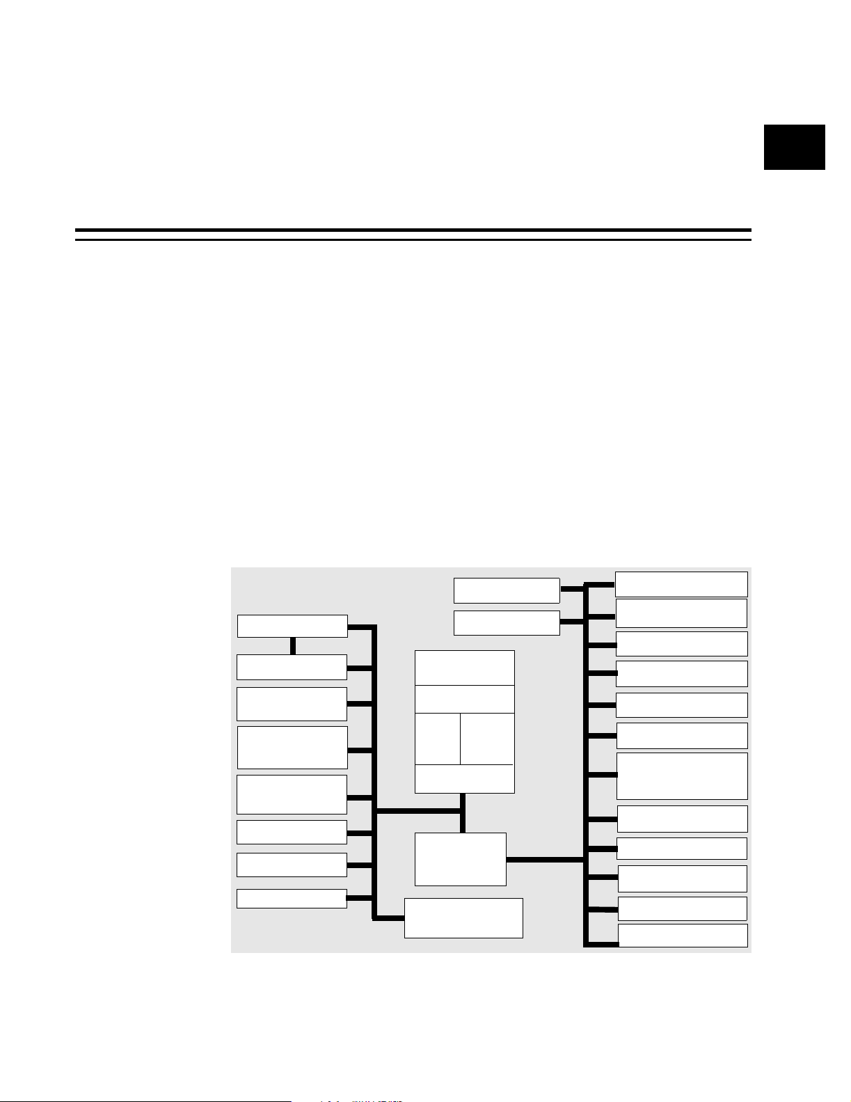
NN
1.1 Introduction
The EP9307 is a highly integrated system-on-chip processor that paves the
way for a multitude of next-generation consumer and industrial electronic
products. Designers of digital media servers and jukeboxes, telematic control
systems, thin clients, set-top boxes, point-of-sale terminals, industrial controls,
biometric security systems, and GPS devices will benefit from the EP9307’s
integrated architecture and advanced features. In fact, with amazingly agile
performance provided by a 200 MHz ARM920T processor, and featuring an
incredibly wide breadth of peripheral interfaces, the EP9307 is well suited to
an even broader range of high volume applications. Furthermore, by enabling
or disabling the EP9307’s peripheral interfaces, designers can reduce
development costs and accelerate time-to-market by creating a single platform
that can be easily modified to deliver a variety of differentiated end products.
Figure 1-1. EP9307 Block Diagram
Chapter 1
1Introduction
1
18-bit Raster LCD
SDRAM
SRAM/FLASH/
ROM
12 Channel DMA
Engine
1/10/100 Ethernet
MAC
JTAG
USB Host, 3 Ports
Boot ROM
UART1 w/ HDLC
UART3 w/ HDLC
MaverickCrunch
Coprocessor
ARM920T
I-Cache
AMBA High-Speed Bus (AHB)
Vectored Interrupt
Controllers (2)
D-Cache
16KB
AHB/APB
16KB
MMU
Bridge
UART2 w/ IrDA
System Ctrl - PLLs (2)
Touch Screen ADC
TM
8x8 Key Scan
PWM
2
S (IIS)
I
Enhanced GPIO
EEPROM, LED (2)
SPI
AMBA Peripheral Bus (APB)
AC’97
RTC with Trim
Watchdog Timer
Timers
EP9307 User’s Manual - DS667UM1 29
Copyright 2004 Cirrus Logic
Page 30

Introduction
1 1.2 EP9307 Features
The EP9307 system-on-chip processor has the following features:
• 200 MHz ARM920T Processor
• 16 KByte data cache and 16 KByte instruction cache
• MMU enabling Linux
• 100 MHz system bus
• MaverickCrunch
• Floating point, integer and signal processing instructions
• Optimized for digital music compression algorithms
• Hardware interlocks allow in-line coding
• MaverickKey
• 32-bit unique ID
• 128-bit random ID
• Integrated Peripheral Interfaces
• EIDE, up to 2 devices
• 1/10/100 Mbps Ethernet MAC
• Three-port USB 2.0 Full Speed host (OHCI)
• Three UARTs (16550 Type)
• IrDA interface, slow and fast mode
™
™
IDs for Digital Rights Management or Design IP Security
®
and Windows® CE
Coprocessor
• LCD and Raster Interface with Graphics Accelerator
• Touch screen interface
•SPI port
• AC ‘97 interface
• I2S interface, up to 6 channels
• 8x8 keypad scanner
• External Memory Options
• 32-bit SDRAM interface, up to four banks
• 32/16/8-bit SRAM/Flash/ROM interface (I/F)
• Serial EEPROM interface
30 EP9307 User’s Manual - DS667UM1
Copyright 2004 Cirrus Logic
Page 31

Introduction
NN
• Internal Peripherals
• Real-Time clock with software trim
• 12 DMA channels for data transfer that maximizes system
performance
•Boot ROM
• Dual PLLs control all clock domains
• Watchdog timer
• Two general purpose 16-bit timers
• General purpose 32-bit timer
• 40-bit debug timer
• General-Purpose I/Os
• 16 enhanced GPIOs including interrupt capability
• 31 additional optional GPIOs multiplexed on peripherals
• Available in 272-pin TFBGA package
1.3 EP9307 Applications
1
The EP9307 can be used in a variety of applications, such as:
• Digital media servers
• Integrated home media gateways
• Digital audio jukeboxes
• Portable audio/video players
• Streaming audio/video players
• Telematic control systems
• Set-top boxes
• Point-of-sale terminals
• Thin clients
• Internet TVs
• Biometric security systems
• Industrial controls
• GPS & fleet management systems
• Educational toys
• Voting machines
• Medical equipment
EP9307 User’s Manual - DS667UM1 31
Copyright 2004 Cirrus Logic
Page 32

Introduction
1 1.4 Overview of EP9307 Features
1.4.1 High-Performance ARM920T Processor Core
The EP9307 features an advanced ARM920T processor design with an MMU
that supports Linux®, Windows® CE, and many other embedded operating
systems. The ARM920T’s 32-bit microcontroller architecture, with a five-stage
pipeline, delivers impressive performance at very low power. The included 16
KByte instruction cache and 16 KByte data cache provide zero-cycle latency
to the current program and data, or can be locked to provide guaranteed nolatency access to critical instructions and data. For applications with
instruction memory size restrictions, the ARM920T’s compressed Thumb
instruction set provides a space-efficient design that maximizes external
instruction memory usage.
1.4.2 MaverickCrunch™ Coprocessor for Ultra-Fast Math Processing
The MaverickCrunch coprocessor is an advanced, mixed-mode math
coprocessor that greatly accelerates the single and double-precision integer
and floating-point processing capabilities of the ARM920T processor core.
The engine simplifies the end-user’s programming task by using predefined
coprocessor instructions, by utilizing standard ARM compiler tools, and by
requiring just one debugger session for the entire system. Furthermore, the
integrated design provides a single instruction stream and the advantage of
zero latency for cached instructions. To emulate this capability, competitors’
solutions add a DSP to the system, which requires separate
compiler/linker/debugger tool sets. This additional DSP requires programmers
to write two separate programs and debug them simultaneously, which can
result in frustration and costly delays.
®
The single-cycle integer multiply-accumulate instruction in the
MaverickCrunch coprocessor allows the EP9307 to offer unique speed and
performance while encoding digital audio and video formats, processing data
via Ethernet, and performing other math-intensive computing and dataprocessing functions in consumer and industrial electronics.
1.4.3 MaverickKey™ Unique ID Secures Digital Content and OEM Designs
MaverickKey unique hardware programmed IDs provide an excellent solution
to the growing concern over secure Web content and commerce. With Internet
security playing an important role in the delivery of digital media such as books
or music, traditional software methods are quickly becoming unreliable. The
MaverickKey unique IDs provide OEMs with a method of utilizing specific
hardware IDs for DRM (Digital Rights Management) mechanisms.
32 EP9307 User’s Manual - DS667UM1
Copyright 2004 Cirrus Logic
Page 33

Introduction
NN
MaverickKey uses a specific 32-bit ID and a 128-bit random ID that are
programmed into the EP9307 through the use of laser probing technology.
These IDs can then be used to match secure copyrighted content with the ID
of the target device that the EP9307 is powering, and then deliver the
copyrighted information over a secure connection. In addition, secure
transactions can benefit by matching device IDs to server IDs.
MaverickKey IDs can also be used by OEMs and design houses to protect
against design piracy by presetting ranges for unique IDs. For more
information on securing your design using MaverickKey, please contact your
Cirrus Logic sales representative.
1.4.4 Integrated Three-port USB 2.0 Full Speed Host with Transceivers
The EP9307 integrates three USB 2.0 Full Speed host ports. Fully compliant
to the OHCI USB 2.0 Full Speed specification (12 Mbps), the host ports can be
used to provide connections to a number of external devices including mass
storage devices, external portable devices such as audio players or cameras,
printers, or USB hubs. Naturally, the three-port USB host also supports the
USB 2.0 Low Speed standard. This provides the opportunity to create a wide
array of flexible system configurations.
1.4.5 Integrated Ethernet MAC Reduces BOM Costs
1
The EP9307 integrates a 1/10/100 Mbps Ethernet Media Access Controller
(MAC) on the device. With a simple connection to an MII-based external PHY,
an EP9307-based system has easy, high-performance, cost-effective Internet
capability.
1.4.6 8x8 Keypad Interface Reduces BOM Costs
The keypad circuitry scans an 8x8 array of 64 normally open, single pole
switches. Any one or two keys depressed will be de-bounced and decoded.
An interrupt is generated whenever a stable set of depressed keys is detected.
If the keypad is not utilized, the 16 column/row pins may be used as generalpurpose I/Os.
1.4.7 Multiple Booting Mechanisms Increase Flexibility
The processor includes a 16 KByte boot ROM to set up standard
configurations. Optionally, the processor may be booted from FLASH memory,
over the SPI serial interface, or through the UART. This boot flexibility makes it
easy to design user-controlled, field-upgradable systems. See Chapter 3 on
page 87, for additional details.
EP9307 User’s Manual - DS667UM1 33
Copyright 2004 Cirrus Logic
Page 34

Introduction
1
1.4.8 Abundant General Purpose I/Os Build Flexible Systems
The EP9307 includes both enhanced and standard general-purpose I/O pins
(GPIOs). The 16 different enhanced GPIOs may individually be configured as
inputs, outputs, or interrupt-enabled inputs. There are an additional 31
standard GPIOs that may individually be used as inputs, outputs, or opendrain pins. The standard GPIOs are multiplexed with peripheral function pins,
so the number available depends on the utilization of peripherals. Together,
the enhanced and standard GPIOs facilitate easy system design with external
peripherals not integrated on the EP9307.
1.4.9 General-Purpose Memory Interface (SDRAM, SRAM, ROM and FLASH)
The EP9307 features a unified memory address model in which all memory
devices are accessed over a common address/data bus. A separate internal
bus is dedicated to the read-only Raster/Display refresh engine, while the rest
of the memory accesses are performed via the high-speed processor bus. The
SRAM memory controller supports 8, 16 and 32-bit devices and
accommodates an internal boot ROM concurrently with a 32-bit SDRAM
memory.
1.4.10 12-Bit Analog-to-Digital Converter (ADC) Provides an Integrated
Touch-Screen Interface or General ADC Functionality
The EP9307 includes a 12-bit ADC, which can be utilized either as a touchscreen interface or for general ADC functionality. The touch-screen interface
performs all sampling, averaging, ADC range checking, and control for a wide
variety of analog-resistive touchscreens. To improve system performance, the
controller only interrupts the processor when a meaningful change occurs.
The touch-screen hardware may be disabled, and the switch matrix and ADC
controlled directly for general ADC usage if desired.
1.4.11 Graphics Accelerator
The EP9307 includes a hardware graphics acceleration engine that improves
graphic performance by handling block copy, block fill and hardware line draw
operations. The graphics accelerator is used in the system to off load graphics
operations from the processor.
34 EP9307 User’s Manual - DS667UM1
Copyright 2004 Cirrus Logic
Page 35

Chapter 2
OO
2.1 Introduction
The MaverickCrunch coprocessor accelerates IEEE-754 floating point
arithmetic and 32-bit and 64-bit fixed point arithmetic operations. It provides
an integer multiply-accumulate (MAC) that is considerably faster than the
native MAC implementation in the ARM920T. The MaverickCrunch
coprocessor significantly accelerates the arithmetic processing required to
encode/decode digital audio formats.
The MaverickCrunch coprocessor uses the standard ARM920T coprocessor
interface, sharing its memory interface and instruction stream. All
MaverickCrunch operations are simply ARM920T coprocessor instructions.
The coprocessor handles all internal inter-instruction dependencies by using
internal data forwarding and inserting wait states.
2.1.1 Features
Key features include:
2MaverickCrunch Coprocessor
2
• IEEE-754 single and double precision floating point
• 32/64-bit integer
• Add/multiply/compare
• Integer Multiply-Accumulate (MAC) 32-bit input with 72-bit accumulate
• Integer Shifts
• Floating point to/from integer conversion
• Sixteen 64-bit registers
• Four 72-bit accumulators
2.1.2 Operational Overview
The MaverickCrunch coprocessor is a true ARM920T coprocessor. It
communicates with the ARM920T via the coprocessor bus and shares the
instruction stream and memory interface of the ARM920T. It runs at the
ARM920T core clock frequency (either FCLK or BCLK).
The coprocessor supports four primary data formats:
EP9307 User’s Manual - DS667UM1 35
Copyright 2004 Cirrus Logic
Page 36

MaverickCrunch Coprocessor
• IEEE-754 single precision floating point (24-bit signed significand and 8bit biased exponent)
2
• IEEE-754 double precision floating point (53-bit signed significand and
11-bit biased exponent)
• 32-bit integer
• 64-bit integer
The coprocessor performs the following standard operations on all four
supported data formats:
• addition
• subtraction
• multiplication
• absolute value
• negation
• logical left/right shift
• comparison
In addition, for 32-bit integers, the coprocessor provides:
• multiply-accumulate (MAC)
• multiply-subtract (MSB)
Any of the four data formats may be converted to another of the formats. All
four data types may be loaded directly from and stored directly to memory via
the ARM920T coprocessor interface. They may also be moved to or from
ARM920T registers.
The MaverickCrunch coprocessor also provides a 72-bit extended precision
integer format that is used only in the accumulators. The accumulators may
also be used in MAC and MSB operations.
IEEE-754 rounding and exceptions are also provided. Four rounding modes
for floating point operations are:
• round to nearest
• round toward
• round toward -∞
• round toward 0
Exceptions include:
• Invalid operator
•Overflow
+∞
36 EP9307 User’s Manual - DS667UM1
Copyright 2004 Cirrus Logic
Page 37

• Underflow
• Inexact
MaverickCrunch Coprocessor
OO
Note that the division by zero exception is not supported as the
MaverickCrunch coprocessor does not provide division or square root.
2.1.3 Pipelines and Latency
There are two primary pipelines within the MaverickCrunch coprocessor. One
handles all communication with the ARM920T, while the other, the “data path”
pipeline, handles all arithmetic operations (this one actually operates at one
half the MaverickCrunch coprocessor clock frequency).
The data path pipeline may run synchronously or asynchronously with respect
to the ARM instruction pipeline. If run asynchronously, data path computation
is decoupled from the ARM, allowing high throughput, though arithmetic
exceptions are not synchronous. If run synchronously, exceptions are
synchronous, but throughput suffers.
Assuming no inter-instruction dependencies causing pipeline stalls, arithmetic
instructions can produce a new result every two ARM920T clocks which is a
maximum throughput of one data path instruction per eight ARM920T clocks.
The only exception is 64-bit multiplies (CFMULD or CFMUL64), which require
six extra ARM920T clocks to produce their result, which is maximum
throughput of eight ARM920T clocks per instruction.
The normal latency for an arithmetic instruction is approximately nine
ARM920T clocks, from initial decode to the time the result is written to the
register file. A 64-bit multiply requires 15 clocks.
2
2.1.4 Data Registers
The MaverickCrunch coprocessor contains the following registers:
• 16 64-bit general purpose registers, c0 through c15
• 4 72-bit accumulators, a0 through a3
• 1 status and control register, DSPSC
A single precision floating point value is stored in the upper 32 bits of a 64-bit
register and must be explicitly promoted to double precision to be used in
double precision calculations:
63 62 55 32 31 0
Sign Exponent Significand
EP9307 User’s Manual - DS667UM1 37
Copyright 2004 Cirrus Logic
not used
Page 38
2
MaverickCrunch Coprocessor
A double precision value requires all 64 bits:
63 62 52 51 0
Sign Exponent Significand
A 32-bit integer is stored in the lower 32 bits of a 64-bit register and signextended when written, provided the UI bit in the DSPSC is clear:
63 32 31 30 0
Sign Extension Sign Data
Hence, 32-bit integers may be used directly in calculations with 64-bit
integers, which are stored as shown:
63 62 0
Sign Data
2.1.5 Integer Saturation Arithmetic
By default, the coprocessor treats all 32-bit and 64-bit integers as signed
values and automatically saturates the results of most integer operations and
all conversions from floating-point to integer format. Instructions that may
saturate their results are:
• CFADD32 and CFADD64
• CFSUB32 and CFSUB64
• CFMUL32 and CFMUL64
• CFMAC32 and CFMSC32
• CFCVTS32 and CFCVTD32
• CFTRUNCS32 and CFTRUNCD32
This behavior, however, can be altered by setting the UI bit and the ISAT bit in
the DSPSC. With the UI bit clear (the default), 32-bit and 64-bit integer
operations are treated as signed with respect to overflow and underflow
detection and saturation as well as compare operations. Setting the UI bit
causes the MaverickCrunch coprocessor to treat all 32-bit and 64-bit integer
operations as unsigned with respect to overflow, underflow, saturation, and
comparison.
With saturation enabled (the default), the maximum representable value is
returned on overflow and the minimum representable value is returned on
38 EP9307 User’s Manual - DS667UM1
Copyright 2004 Cirrus Logic
Page 39

underflow. The maximum and minimum values depends on the operand size
and whether the UI bit in the DSPSC is set, as shown in Table 2-1.
Table 2-1: Saturation for Non-accumulator Instructions
Signed
Overflow
Unsigned
Signed
Underflow
Unsigned
To disable saturation on overflow and underflow, set the ISAT bit in the
DSPSC.
Normally, arithmetic instructions that write to an accumulator do not saturate
their results on overflow or underflow. These instructions are:
• CFMADD32 and CFMSUB32
• CFMADDA32 and CFMSUBA32
MaverickCrunch Coprocessor
32-bit 0x7FFF_FFFF
64-bit 0x7FFF_FFFF_FFFF_FFFF
32-bit 0xFFFF_FFFF
64-bit 0xFFFF_FFFF_FFFF_FFFF
32-bit 0x8000_0000
64-bit 0x8000_0000_0000_0000
32-bit 0x0000_0000
64-bit 0x0000_0000_0000_0000
OO
2
However, the SAT[1:0] bits in the DSPSC may be set to select one of several
kinds of saturation to occur on the results of these instructions before they are
written to an accumulator.
Note: This action does not affect the operation of instructions that do not write their
result to an accumulator.
Enabling saturation also modifies the representation of data stored in the
accumulator. The three supported bit formats and their maximum and
minimum saturation values are shown in Table 2-2 on page 39.
Table 2-2: Accumulator Bit Formats for Saturation
Bit Format Maximum Value (hex) Minimum Value (hex)
2.62 64 bits - 0x3FFF FFFF FFFF FFFF 64 bits - 0xC000 0000 0000 0000
1.63 64 bits - 0x7FFF FFFF FFFF FFFF 64 bits - 0x8000 0000 0000 0000
1.31 32 bits - 0x7FFF FFFF 32 bits - 0x8000 0000
The bit format x.yy represents x binary bits before the decimal point and yy
fraction bits after decimal point, as for example, when the bit format 2.62 has
two binary bits and sixty-two fraction bits. Though these formats utilize either
32- or 64-bit integers, the accumulators are 72 bits wide. If the accumulator
saturation mode is disabled (the default), the accumulator bit fields are
assigned as below for a 2’s complement integer.
71 70 0
Sign Data
EP9307 User’s Manual - DS667UM1 39
Copyright 2004 Cirrus Logic
Page 40
2
MaverickCrunch Coprocessor
If the saturation mode 1.63 is selected, the bit field assignments are:
71 64 63 62 0
Sign Extension Sign Data
If the saturation mode 1.31 is selected, the bit field assignments are:
71 64 63 62 32 31 0
Sign Extension Sign Data Unused
If the saturation mode 2.62 is selected, the bit field assignments are:
71 63 62 61 0
Sign Extension Sign Data
2.1.6 Comparisons
The Crunch coprocessor provides four compare operations:
• CFCMP32 - 32-bit integer
• CFCMP64 - 64-bit integer
• CFCMPS - single floating point
• CFCMPD - double floating point
The DSPSC register bit UINT affects the operation of integer comparisons. If
clear, integers are treated as signed values, and if set, they are treated as
unsigned. DSPSC.UINT has no effect on floating point comparisons.
All compare operations update both the FCC[1:0] bits in the DSPSC register
and an ARM register. Though any of the ARM general purpose registers r0
through r14 may be specified as the destination, specifying r15 actually
updates the CPSR flag bits NZCV. This permits the condition code field of any
subsequent ARM instruction to gate the execution of that instruction based on
the result of a Crunch compare operation.
Table 2-3 on page 41 illustrates the legal relationships and, for each one, the
values written to the FCC bits and the NZCV flags. The FCC bits and the
NZCV flags provide the same information, but in different ways and in different
places. Their values depend only on the relationship between the operands,
regardless of whether the operands are considered signed integer, unsigned
integer, or floating point. The unordered relationship can only apply to floating
point operands.
40 EP9307 User’s Manual - DS667UM1
Copyright 2004 Cirrus Logic
Page 41

Table 2-3: Comparison Relationships and Their Results
Relationship FCC[1:0] NCZV
AB=
MaverickCrunch Coprocessor
00 0100
OO
2
AB<
AB>
Unordered 11 0000
The NZCV flags are not computed exactly as with integer comparisons using
the ARM CMP instruction. Hence, when examining the result of Crunch
comparisons, the condition codes field of ARM instructions should be
interpreted differently, as shown in Table 2-4 on page 41. The same six
condition codes should be used whether the comparison operands were
signed integers, unsigned integers, or floating point. No other condition codes
are meaningful.
Table 2-4: ARM Condition Codes and Crunch Compare Results
Condition Code
Opcode[31:28] Mnemonic
0000 EQ Equal Equal
0001 NE Not Equal Not Equal
1010 GE Signed Greater Than or Equal Greater Than or Equal
1011 LT Signed Less Than Less Than
Relationship ARM Meaning Crunch Meaning
AB=
AB≠
AB≥
AB<
01 1000
10 1001
1100 GT Signed Greater Than Greater Than
1101 LE Signed Less Than or Equal Less Than or Equal
1110 AL N/A Always (unconditional) Always (unconditional)
1111 NV N/A Never Never
AB>
A B≤
2.2 Programming Examples
The examples below show two algorithms, each implemented using the
standard programming languages and the MaverickCrunch instruction set.
2.2.1 Example 1
Sections 2.2.1.2, 2.2.1.3, and 2.2.1.4, show three coding samples performing
the same operation. Section 2.2.1.1 on page 42 shows common setup code
used by all three samples. Section 2.2.1.2 on page 42 shows the program
implemented in C code. Section 2.2.1.3 on page 42 uses ARM assembly
language, accessing the MaverickCrunch with ARM coprocessor instructions.
EP9307 User’s Manual - DS667UM1 41
Copyright 2004 Cirrus Logic
Page 42

MaverickCrunch Coprocessor
Section 2.2.1.4 on page 42 uses MaverickCrunch assembly language
instructions.
2
2.2.1.1 Setup Code
ldr r0, =80930000 ; Syscon base address
mov r1, #0xaa ; SW lock key
str r1, [r0, #0xc0] ; unlock by writing key to SysSWLock register
ldr r1, [r0, #0x80] ; Turn on CPENA bit in DEVCFG register to
orr r1, r1, #0x00800000 ; enable MaverickCrunch coprocessor
str r1, [r0, #0x80] ;
2.2.1.2 C Code
int num = 0;
for(num=0; num < 10; num++)
num = num * 5;
2.2.1.3 Accessing MaverickCrunch with ARM Coprocessor Instructions
ldc p5, c0, [r0, #0x0] ; data section preloaded with 0x0 (“num”)
ldc p5, c1, [r0, #0x4] ; data section preloaded with 0xa
ldc p5, c2, [r0, #0x8] ; data section preloaded with 0x1
ldc p5, c3, [r0, #0xc] ; data section preloaded with 0x5
loop
cdp p5, 1, c0, c0, c3, 0 ; c0 <= c0 * 5
cdp p5, 3, c0, c0, c2, 6 ; c0 <= c0 - 1
mrc p5, 0, r15 c0, c1, 4 ; c0 < 10 ?
blt loop ; yes
stc p5, c0, [r0, #0x0] ; no, store result
2.2.1.4 MaverickCrunch Assembly Language Instructions
cfldr32 c0, [r0, #0x0] ; data section preloaded with 0x0 (“num”)
cfldr32 c1, [r0, #0x4] ; data section preloaded with 0xa
cfldr32 c2, [r0, #0x8] ; data section preloaded with 0x1
cfldr32 c3, [r0, #0xc] ; data section preloaded with 0x5
loop
cfmul32 c0, c0, c3 ; c0 <= c0 * 5
cfsub32 c0, c0, c2 ; c0 <= c0 - 1
cfcmp32 r15, c0, c1 ; c0 < 10 ?
blt loop ; yes
cfstr32 c0, [r0, #0x0] ; no, store result
2.2.2 Example 2
The following function performs an FIR filter on the given input stream. The
variable “data” points to an array of floating point values to be filtered, “n” is the
number of samples for which the filter should be applied, “filter” is the FIR filter
42 EP9307 User’s Manual - DS667UM1
Copyright 2004 Cirrus Logic
Page 43

MaverickCrunch Coprocessor
to be applied, and “m” is the number of taps in the FIR filter. The “data” array
must be “n + m - 1” samples in length, and “n” samples will be produced.
OO
2.2.2.1 C Code
void
ComputeFIR(float *data, int n, float *filter, int m)
{
int i, j;
float sum;
for(i = 0; i < n; i++)
{
sum = 0;
for(j = 0; j < m; j++)
{
sum += data[i + j] * filter[j];
}
data[i] = sum;
}
}
2.2.2.2 MaverickCrunch Assembly Language Instructions
2
ComputeFIR
mov r1, r1, lsl #2 ; n *= 4
mov r3, r3, lsl #2 ; m *= 4
outer_loop
mov r12, r3 ; j = m * 4
cfsub64 c0, c0, c0 ; int_sum = 0;
cfcvt32s c0, c0 ; sum = float(int_sum);
inner_loop
cfldrs c2, [r0], #4 ; c2 = *data++;
cfldrs c3, [r2], #4 ; c3 = *filter++;
cfmuls c1, c2, c3 ; c1 = c2 * c3;
cfadds c0, c0, c1 ; sum += c1;
subs r12, r12, #4 ; j -= 4;
bne inner_loop ; branch if j != 0
sub r0, r3 ; data -= m * 4;
cfstrs c0, [r0], #4 ; *data++ = sum;
sub r2, r3 ; filter -= m * 4;
subs r1, r1, #4 ; n -= 4;
bne outer_loop ; branch if n != 0
mov pc, lr ; return to caller
EP9307 User’s Manual - DS667UM1 43
Copyright 2004 Cirrus Logic
Page 44

2
MaverickCrunch Coprocessor
2.3 DSPSC Register
63 62 61 60 59 58 57 56 55 54 53 52 51 50 49 48
INST
47 46 45 44 43 42 41 40 39 38 37 36 35 34 33 32
INST
31 30 29 28 27 26 25 24 23 22 21 20 19 18 17 16
DAID HVID RSVD ISAT UI INT AEXC SAT[1:0] FCC[1:0]
15 14 13 12 11 10 9 8 7 6 5 4 3 2 1 0
V FWDEN Invalid Denorm RM[1:0] IXE UFE OFE RSVD IOE IX UF OF RSVD IO
Default:
Definition:
Bit Descriptions:
0x0000_0000_0000_0000
MaverickCrunch Status and Control Register. Accessed only via the
MaverickCrunch instruction set. All bits, including status bits, are both
readable and writable. This register should generally be written only using a
read-modify-write sequence.
RSVD: Reserved. Unknown During Read.
INST: Exception Instruction. Whenever an unmasked exception
occurs, these 32 bits are loaded with the instruction that
caused the exception. Hence, this contains the instruction
that caused the most recent unmasked exception.
DAID: MaverickCrunch Architecture ID. This read-only value is
incremented for each revision of the overall
MaverickCrunch coprocessor architecture. These bits are
“000” for this revision.
HVID: Hardware Version ID. This read-only value is incremented
each time the hardware implementation of the architecture
named by DAID[2:0] is changed, typically done in
response to bugs. These bits are “000” for this version.
44 EP9307 User’s Manual - DS667UM1
Copyright 2004 Cirrus Logic
Page 45

MaverickCrunch Coprocessor
ISAT: Integer Saturate Enable. This bit controls whether non-
accumulator integer operations, both signed and
unsigned, will saturate on overflow or underflow.
0 = Saturation enabled.
1 = Saturation disabled.
UI: Unsigned Integer Enable. This bit controls whether non-
accumulator integer operations treat their operands as
signed or unsigned. It also determines the saturation value
if the ISAT bit is clear.
0 = Signed integers.
1 = Unsigned integers.
INT: MaverickCrunch Interrupt. This bit indicates whether an
interrupt has occurred. This bit is identical to the external
interrupt signal.
0 = No interrupt signaled.
1 = Interrupt signaled.
OO
2
AEXC: Asynchronous Exception Enable. This bit determines
whether exceptions generated by the coprocessor are
signaled synchronously or asynchronously to the
ARM920T. Synchronous exceptions force all data path
instructions to be serialized and to stall the ARM920T. If
exceptions are asynchronous, they are signalled by
assertion of the DSPINT output of the coprocessor, which
may interrupt the ARM920T via the interrupt controller.
Enabling asynchronous exceptions does provide a
performance improvement, but makes it difficult for an
interrupt handler to determine the coprocessor instruction
that caused the exception because the address of the
instruction is not preserved. Exceptions may be
individually enabled by other bits in this register (IXE, UFE,
OFE, and IOE). This bit has no effect if no exceptions are
enabled.
0 = Exceptions are synchronous.
1 = Exceptions are asynchronous
SAT[1:0]: Accumulator saturation mode select. These bits are set to
select the saturation mode or to disable the saturation for
accumulator operations.
0X = Saturation disabled for accumulator operations
10 = Accumulator saturation enabled, bit formats 1.63 and
1.31
11 = Accumulator saturation enabled, bit format 2.62
EP9307 User’s Manual - DS667UM1 45
Copyright 2004 Cirrus Logic
Page 46

2
MaverickCrunch Coprocessor
FCC[1:0]: FCC flags out of comparator.
00 = Operand A equals operand B.
01 = Operand A less than operand B.
10 = Operand A greater than operand B.
11 = Operands are unordered (at least one is NaN).
V: Overflow Flag. Indicates the overflow status of the
previous integer operation.
0 = No overflow.
1 = Overflow.
FWDEN: Forwarding Enable. This bit determines whether data path
writeback results are forwarded to the data path operand
fetch stage and to the STC/MRC execute stage. When
pipeline interlocks occur due to dependencies of data
path, STC, and MRC instruction source operands on data
path results, setting this bit will improve instruction
throughput.
0 = Forwarding not enabled.
1 = Forwarding enabled.
Invalid: 0 = No invalid operations detected
1 = An invalid operation was performed.
Denorm: 0 = No denormalized numbers have been supplied as
instruction operands
1 = a denormalized number has been supplied as an
instruction operand.
RM[1:0]: Rounding Mode. Selects IEEE 754 rounding mode.
0 0 = Round to nearest.
0 1 = Round toward 0.
1 0 = Round to
1 1 = Round to
IXE: Inexact Trap Enable. Enables/disables software trapping
for IEEE 754 inexact exceptions.
0 = Disable software trapping for inexact exceptions.
1 = Enable software trapping for inexact exceptions.
UFE: Underflow Trap Enable. Enables/disables software
trapping for IEEE 754 underflow exceptions.
0 = Disable software trapping for underflow exceptions.
1 = Enable software trapping for underflow exceptions.
OFE: Overflow Trap Enable. Enables/disables software trapping
for IEEE 754 overflow exceptions.
0 = Disable software trapping for overflow exceptions.
1 = Enable software trapping for overflow exceptions.
-∞.
+∞.
46 EP9307 User’s Manual - DS667UM1
Copyright 2004 Cirrus Logic
Page 47

MaverickCrunch Coprocessor
IOE: Invalid Operator Trap Enable. Enables/disables software
trapping for IEEE 754 invalid operator exceptions.
0 = Disable software trapping for invalid operator
exceptions.
1 = Enable software trapping for invalid operator
exceptions.
IX: Inexact. Set when an IEEE 754 inexact exception occurs,
regardless of whether or not software trapping for inexact
exceptions is enabled. Writing a “0” to this position clears
the status bit.
0 = No inexact exception detected.
1 = Inexact exception detected.
UF: Underflow. Set when an IEEE 754 underflow exception
occurs, regardless of whether or not software trapping for
underflow exceptions is enabled. Writing a “0” to this
position clears the status bit.
0 = No underflow exception detected.
1 = Underflow exception detected.
OO
2
OF: Overflow. Set when an IEEE 754 overflow exception
occurs, regardless of whether or not software trapping for
overflow exceptions is enabled. Writing a “0” to this
position clears the status bit.
0 = No overflow exception detected.
1 = Overflow exception detected.
IO: Invalid Operator. Set when an IEEE 754 invalid operator
exception occurs, regardless of whether or not software
trapping for invalid operator exceptions is enabled. Writing
a “0” to this position clears the status bit.
0 = No invalid operator exception detected.
1 = Invalid operator exception detected.
2.4 ARM Coprocessor Instruction Format
The ARM V4T architecture defines five ARM coprocessor instructions:
• CDP - Coprocessor Data Processing
• LDC - Load Coprocessor
• STC - Store Coprocessor
• MCR - Move to Coprocessor Register from ARM Register
• MRC - Move to ARM Register from Coprocessor Register
The coprocessor instruction assembler notation is found in the ARM
programming manuals or the Quick Reference Card. (For additional
EP9307 User’s Manual - DS667UM1 47
Copyright 2004 Cirrus Logic
Page 48

MaverickCrunch Coprocessor
information, see “Reference Documents”, item 4, on page 5.) Formats for the
above instructions and variants of these instructions are detailed below.
2
CDP (Coprocessor Data Processing) Instruction Format
31 28 27 24 23 20 19 16 15 12 11 8 7 5 4 3 0
cond 1110 opcode1 CRn CRd cp num opcode2 0 CRm
LDC (Load Coprocessor) Instruction Format
31 28 27 25 24 23 22 21 20 19 16 15 12 11 8 7 0
cond 110 P U N W 1 Rn CRd cp num offset
STC (Store Coprocessor) Instruction Format
31 28 27 25 24 23 22 21 20 19 16 15 12 11 8 7 0
cond 110 P U N W 0 Rn CRd cp num offset
MCR (Move to Coprocessor from ARM Register) Instruction Format
31 28 27 24 23 21 20 19 16 15 12 11 8 7 5 4 3 0
cond 1110 opcode1 0 CRn Rd cp num opcode2 1 CRm
MRC (Move to ARM Register from Coprocessor) Instruction Format
31 28 27 24 23 21 20 19 16 15 12 11 8 7 5 4 3 0
cond 1110 opcode1 1 CRn Rd cp num opcode2 1 CRm
48 EP9307 User’s Manual - DS667UM1
Copyright 2004 Cirrus Logic
Page 49
MaverickCrunch Coprocessor
Table 2-5 shows the condition codes, which are bits [31:28] for each
instruction format.
OO
Table 2-5: Condition Code Definitions
Cond
[31:28]
0000 EQ Equal Z set
0001 NE Not Equal Z clear
0010 CS/HS Carry Set/Unsigned H igher or Same C set
0011 CC/LO Carry Clear/Unsigned Lower C clear
0100 MI Minus/Negative N set
0101 PL Plus/Positive or Zero N clear
0110 VS Overflow V set
0111 VC No Overflow V clear
1000 HI Unsigned Higher C set and Z clear
1001 LS Unsigned Lower or Same C clear or Z set
1010 GE Signed Greater Than or Equal N set and V set, or N clear and V clear (N = V)
1011 LT Signed Less Than N set and V clear, or N clear and V set (N ! = V)
1100 GT Signed Greater Than Z clear, and either N set and V set, or N clear and V clear (Z = 0, N = V)
1101 LE Signed Less Than or Equal Z set, or N set and V clear, or N clear and V set (Z = 1, N ! = V)
1110 AL Always (unconditional) -
Mnemonic
Extension
1111 NV Ne ver -
Meaning Status Flag State
2
The remaining bits in the instruction formats are interpreted as follows:
• opcode1: MaverickCrunch coprocessor-defined opcode.
• opcode2: MaverickCrunch coprocessor-defined opcode.
• CRn: MaverickCrunch coprocessor-defined register ID.
• CRd: MaverickCrunch coprocessor-defined register ID.
• CRm: MaverickCrunch coprocessor-defined register ID.
• Rn: Specifies an ARM base address register. These bits are ignored by
the MaverickCrunch coprocessor.
• Rd: Specifies a source or destination ARM register.
• cp_num: Coprocessor number.
• P: Pre-indexing (P=1) or post-indexing (P=0) addressing. This bit is
ignored by the MaverickCrunch coprocessor.
• U: Specifies whether the supplied 8-bit offset is added to a base register
EP9307 User’s Manual - DS667UM1 49
Copyright 2004 Cirrus Logic
Page 50
MaverickCrunch Coprocessor
(U=1) or subtracted from a base register (U=0). This bit is ignored by the
MaverickCrunch coprocessor.
2
• N: Specifies the width of a data type involved in a move operation. The
MaverickCrunch coprocessor uses this bit to distinguish between single
precision floating point/32-bit integer numbers (N=0) and double precision
floating point/64-bit integer numbers (N=1).
• W: Specifies whether or not a calculated address is written back to a base
register (W=1) or not (W=0). This bit is ignored by the MaverickCrunch
coprocessor.
• offset: An 8-bit word offset used in address calculations. These bits are
ignored by the MaverickCrunch coprocessor.
Table 2-6, below, and Table 2-7, Table 2-8, and Table 2-9 on page 51, define
the bit values for opcode2, opcode1, and cp_num for all of the
MaverickCrunch instructions.
Table 2-6: LDC/STC Opcode Map
cp num [3:0] Opcode Bits 22 and 20
0100
0101
00 01 10 11
cfstrs
cfstr32
cfldrs
cfldr32
cfstrd
cfstr64
cfldrd
cfldr64
50 EP9307 User’s Manual - DS667UM1
Copyright 2004 Cirrus Logic
Page 51
Table 2-7: CDP Opcode Map
MaverickCrunch Coprocessor
OO
op
code
[1:0]
00
01
10
11
Table 2-8: MCR Opcode Map
cp
num
1
[3:0]
000 001 010 011 100 101 110 111
0100 cfcpys cfcpyd cfcvtds cfcvtsd cfcvt32s cfcvt32d cfcvt64s cfcvt64d
0101 cfsh32
0110 cfmadd32
0100 cfmuls cfmuld cfmv32al cfmv32am cfmv32ah cfmv32a cfmv64a cfmv32sc
0101 cfmul32 cfmul64 cfmac32 cfmsc32 cfcvts32 cfcvtd32 cftruncs32 cftruncd32
0110 cfmsub32
0100 cfmval32 cfmvam32 cfmvah32 cfmva32 cfmva64 cfmvsc32
0101 cfsh64
0110 cfmadda32
0100 cfabss cfabsd cfnegs cfnegd cfadds cfaddd cfsubs cfsubd
0101 cfabs32 cfabs64 cfneg32 cfneg64 cfadd32 cfadd64 cfsub32 cfsub64
0110 cfmsuba32
opcode2[2:0]
2
op
code1cpnum
[3:0]
000 001 010 011 100 101 110 111
0100
0
0101
0110
Table 2-9: MRC Opcode Map
op
code1cpnum
[3:0]
0100
0
0101
0110
cfmvdlr
cfmv64lr
000 001 010 011 100 101 110 111
cfmvrdl
cfmvr64l
cfmvdhr
cfmv64hr
cfmvrdh
cfmvr64h
opcode2[2:0]
cfmvsr
cfrshl32 cfrshl64
opcode2[2:0]
cfmvrs cfcmps
cfcmp32
cfcmpd
cfcmp64
EP9307 User’s Manual - DS667UM1 51
Copyright 2004 Cirrus Logic
Page 52
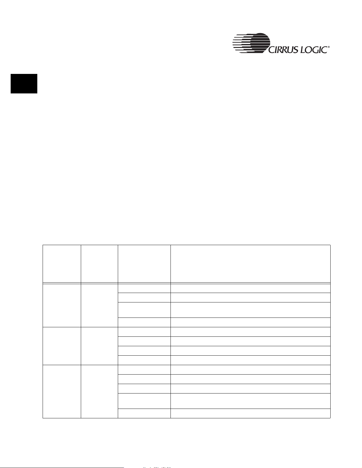
2
MaverickCrunch Coprocessor
2.5 Instruction Set for the MaverickCrunch Coprocessor
Table 2-10 summarizes the MaverickCrunch coprocessor instruction set.
Please note that:
• CRd, CRn, and CRm each refer to any 16 general purpose
MaverickCrunch registers unless otherwise specified
• CRa refers to any of the MaverickCrunch accumulators
• Rd and Rn refer to any of the ARM920T general purpose registers
• <imm> refers to a seven-bit immediate value
The remainder of this section describes in detail each of the individual
MaverickCrunch instructions. The fields in the opcode for each
MaverickCrunch instruction are shown. When specific bit values are required
for the instruction, they are shown as either '1' or '0'. Any field whose value
may vary, such as a register index, is named as in the ARM programming
manuals, and its function described below.
Fields that are ignored by the coprocessor are shaded. Dark shading implies
that a field is processed by the ARM itself and can have any value, while light
shading indicates that the field, though ignored by both the ARM and the
coprocessor, should have the value shown.
Table 2-10: MaverickCrunch Instruction Set
Maverick
Crunch
Coprocessor
Instruction
Type
Loads LDC
Stores STC
Moves to
coprocessor
ARM
Coprocessor
Instruction
Typ e
MCR
Instruction Description
cfldrs CRd, [Rn] Load CRd with single stored at address in Rn
cfldrd CRd, [Rn] Load CRd with double stored at address in Rn
cfldr32 CRd, [Rn]
cfldr64 CRd, [Rn] Load CRd with 64-bit integer stored at address in Rn
cfstrs CRd, [Rn] Store single in CRd at address in Rn
cfstrd CRd, [Rn] Store double in CRd at address in Rn
cflstr32 CRd, [Rn] Store 32-bit integer in CRd at address in Rn
cfstr64 CRd, [Rn] Store 64-bit integer in CRd at address in Rn
cfmvsr CRn, Rd Move single from Rd to CRn[63:32]
cfmvdlr CRn, Rd Move lower half of double from Rd to CRn[31:0]
cfmvdhr CRn, Rd Move upper half of double from Rd to CRn[63:32]
cfmv64lr CRn, Rd
cfmv64hr CRn, Rd Move upper half of 64-bit integer from Rd to CRn[63:32]
Load CRd with 32-bit integer stored at address in Rn, sign extend through
bit 63
Move lower half of 64-bit integer from Rd to CRn[31:0], sign extend bit 31
through bits [63:31]
52 EP9307 User’s Manual - DS667UM1
Copyright 2004 Cirrus Logic
Page 53

Table 2-10: MaverickCrunch Instruction Set (Continued)
MaverickCrunch Coprocessor
OO
Maverick
Crunch
Coprocessor
Instruction
Type
Moves from
coprocessor
Moves to
accumulator
Moves from
accumulator
Move to
DSPSC
Move from
DSPSC
ARM
Coprocessor
Instruction
Typ e
MRC
CDP
CDP
CDP
Instruction Description
cfmvsr Rd, CRn Move single from CRn[63:32] to Rd
cfmvrdl Rd, CRn Move lower half of double from CRn[31:0] to Rd
cfmvrdh Rd, CRn Move upper half of double from CRn[63:32] to Rd
cfmvr64l Rd, CRn Move lower half of 64-bit integer from CRn[31:0] to Rd
cfmvr64h Rd, CRn Move upper half of 64-bit integer from CRn[63:32] to Rd
cfmval32 CRd, CRn Move 32-bit integer from CRn [31:0] to accumulator CRd[31:0]
cfmvam32 CRd, CRn Move 32-bit integer from CRn [31:0] to accumulator CRd[63:32]
cfmvah32 CRd, CRn
cfmva32 CRd, CRn
cfmva64 CRd, CRn
cfmv32al CRd, CRn Move accumulator CRn[31:0] to 32-bit integer CRd[31:0]
cfmv32am CRd, CRn Move accumulator CRn[63:32] to 32-bit integer CRd[31:0]
cfmv32ah CRd, CRn Move accumulator CRn[71:64] to lower 8 bits of 32-bit integer CRd[31:0]
cfmv32a CRd, CRn
cfmv64a CRd, CRn
cfmvsc32 CRd, CRn Move CRd to DSPSC; CRn is ignored
cfmv32sc CRd, CRn Moves DSPSC to CRd; CRn is ignored
Move lower 8 bits of 32-bit integer from CRn [7:0] to accumulator
CRd[71:64]
Move 32-bit integer from CRn[31:0] to accumulator CRd[31:0] and sign
extend through bit 71
Move 64-bit integer from CRn to accumulator CRd[63:0] and sign extend
through bit 71
Saturate to 32-bit integer and move accumulator CRn[31:0] to 32-bit
integer CRd[31:0]
Saturate to 64-bit integer and move accumulator CRn[63:0] to 64-bit
integer CRd
2
EP9307 User’s Manual - DS667UM1 53
Copyright 2004 Cirrus Logic
Page 54
MaverickCrunch Coprocessor
Table 2-10: MaverickCrunch Instruction Set (Continued)
2
Maverick
Crunch
Coprocessor
Instruction
Type
Conversions
and copies
Shifts
Comparisons MRC
Floating point
arithmetic,
single precision
ARM
Coprocessor
Instruction
Typ e
CDP
MCR
CDP
CDP
Instruction Description
cfcpys CRd, CRn Copy a single from CRn to CRd
cfcpyd CRd, CRn Copy a double from CRn to CRd
cfcvtsd CRd, CRn Convert a single in CRn to a double in CRd
cfcvtds CRd, CRn Convert a double in CRn to a single in CRd
cfcvt32s CRd, CRn C onvert a 32-bit integer in CRn to a single in CRd
cfcvt32d CRd, CRn Convert a 32-bit integer in CRn to a double in CRd
cfcvt64s CRd, CRn C onvert a 64-bit integer in CRn to a single in CRd
cfcvt64d CRd, CRn Convert a 64-bit integer in CRn to a double in CRd
cfcvts32 CRd, CRn Convert a single in CRn to a 32-bit integer in CRd
cfcvtd32 CRd, CRn Convert a double in CRn to a 32-bit integer in CRd
cftruncs32 CRd, CRn Truncate a single in CRn to a 32-bit integer in CRd
cftruncd32 CRd, CRn Truncate a double in CRn to a 32-bit integer in CRd
cfrshl32 CRm, CRn, RdShift 32-bit integer in CRn by two’s complement value in Rd and store in
cfrshl64 CRm, CRn, RdShift 64-bit integer in CRn by two’s complement value in Rd and store in
cfsh32 CRd, CRn,
<imm>
cfsh64 CRd, CRn,
<imm>
cfcmps Rd, CRn, CRm Compare singles in CRn to CRm, result in Rd, or CPSR if Rd == R15
cfcmpd Rd, CRn, CRm Compare doubles in CRn to CRm, result in Rd, or CPSR if Rd == R15
cfcmp32 Rd, CRn,
CRm
cfcmp64 Rd, CRn,
CRm
cfabss CRd, CRn CRd gets absolute value of CRn
cfnegs CRd, CRn CRd gets negation of CRn
cfadds CRd, CRn,
CRm
cfsubs CRd, CRn,
CRm
cfmuls CRd, CRn,
CRm
CRm
CRm
Shift 32-bit integer in CRn by <imm> bits and store in CRd, where <imm>
is between -32 and 31, inclusive
Shift 64-bit integer in CRn by <imm> bits and store in CRd, where <imm>
is between -32 and 31, inclusive
Compare 32-bit integers in CRn to CRm, result in Rd, or CPSR if Rd ==
R15
Compare 64-bit integers in CRn to CRm, result in Rd, or CPSR if Rd ==
R15
CRd gets sum of CRn and CRm
CRd gets CRn minus CRm
CRd gets the product of CRn and CRm
54 EP9307 User’s Manual - DS667UM1
Copyright 2004 Cirrus Logic
Page 55
Table 2-10: MaverickCrunch Instruction Set (Continued)
MaverickCrunch Coprocessor
OO
Maverick
Crunch
Coprocessor
Instruction
Type
Floating point
arithmetic,
double
precision
32-bit integer
arithmetic
64-bit integer
arithmetic
Accumulator
arithmetic
ARM
Coprocessor
Instruction
Typ e
CDP
CDP
CDP
CDP
Instruction Description
cfabsd CRd, CRn CRd gets absolute value of CRn
cfnegd CRd, CRn CRd gets negation of CRn
cfaddd CRd, CRn,
CRm
cfsubd CRd, CRn,
CRm
cfmuld CRd, CRn,
CRm
cfabs32 CRd, CRn CRd gets absolute value of CRn
cfneg32 CRd, CRn CRd gets negation of CRn
cfadd32 CRd, CRn,
CRm
cfsub32 CRd, CRn,
CRm
cfmul32 CRd, CRn,
CRm
cfmac32 CRd, CRn,
CRm
cfmsc32 CRD, CRn,
CRm
cfabs64 CRd, CRn CRd gets absolute value of CRn
cfneg64 CRd, CRn CRd gets negation of CRn
cfadd64 CRd, CRn,
CRm
cfsub64 CRd, CRn,
CRm
cfmul64 CRd, CRn,
CRm
cfmadd32 CRa, CRd,
CRn, CRm
cfmsub32 CRa, CRd,
CRn, CRm
cfmadda32 CRa, CRd,
CRn, CRm
cfmsuba32 CRa, CRd,
CRn, CRm
CRd gets sum of CRn and CRm
CRd gets CRn minus CRm
CRd gets the product of CRn and CRm
CRd gets sum of CRn and CRm
CRd gets CRn minus CRm
CRd gets the product of CRn and CRm
CRd gets sum of CRd and the product of CRn and CRm
CRd gets CRd minus the product of CRn and CRm
CRd gets sum of CRn and CRm
CRd gets CRn minus CRm
CRd gets the product of CRn and CRm
Accumulator CRa gets sum of CRd and the product of CRn and CRm
Accumulator CRa gets CRd minus the product of CRn and CRm
Accumulator CRa gets sum of accumulator CRd and the product of CRn
and CRm
Accumulator CRa gets accumulator CRd minus the product of CRn and
CRm
2
EP9307 User’s Manual - DS667UM1 55
Copyright 2004 Cirrus Logic
Page 56
MaverickCrunch Coprocessor
2.5.1 Load and Store Instructions
Loading Floating Point Value from Memory
2
31:28 27:25 24 23 22 21 20 19:16 15:12 11:8 7:0
cond 1 1 0 P UNW1 Rn CRd 0 1 0 0 8_bit_word_offset
Description:
Loads a single or double precision floating point value from memory into
MaverickCrunch register.
Table 2-11: Mnemonic Codes
Mnemonic Addressing Mode N
CFLDRS<cond> CRd, [Rn, <offset>]{!} Immediate pre-indexed 0
CFLDRS<cond> CRd, [Rn], <offset> Immediate post-indexed 0
CFLDRD<cond> CRd, [Rn, <offset>]{!} Immediate pre-indexed 1
CFLDRD<cond> CRd, [Rn], <offset> Immediate post-indexed 1
Bit Definitions:
N: Floating point precision - 0 for single, 1 for double.
Rn: Base register in ARM
CRd: Destination register.
56 EP9307 User’s Manual - DS667UM1
Copyright 2004 Cirrus Logic
Page 57
MaverickCrunch Coprocessor
Loading Integer Value from Memory
31:28 27:25 24 23 22 21 20 19:16 15:12 11:8 7:0
cond 1 1 0 P UNW1 Rn CRd 0 1 0 1 8_bit_word_offset
Description:
Loads a 32- or 64-bit integer from memory into a MaverickCrunch register.
Table 2-12: Mnemonic Codes
Mnemonic Addressing Mode N
CFLDR32<cond> CRd, [Rn, <offset>]{!} Immediate pre-indexed 0
CFLDR32<cond> CRd, [Rn], <offset> Immediate post-indexed 0
CFLDR64<cond> CRd, [Rn, <offset>]{!} Immediate pre-indexed 1
CFLDR64<cond> CRd, [Rn], <offset> Immediate post-indexed 1
Bit Definitions:
OO
2
N: Integer width - 0 for 32-bit integer, 1 for 64-bit integer
Rn: Base register in ARM
CRd: Destination register.
EP9307 User’s Manual - DS667UM1 57
Copyright 2004 Cirrus Logic
Page 58

2
MaverickCrunch Coprocessor
Store Floating Point Values to Memory
31:28 27:25 24 23 22 21 20 19:16 15:12 11:8 7:0
cond 1 1 0 P UNW0 Rn CRd 0 1 0 0 8_bit_word_offset
Description:
Stores a single or double precision floating point value from a MaverickCrunch
register into memory.
Mnemonic:
Mnemonic Addressing Mode N
CFSTRS<cond> CRd, [Rn, <offset>]{!} Immediate pre-indexed 0
CFSTRS <cond> CRd, [Rn], <offset> Immediate post-indexed 0
CFSTRD<cond> CRd, [R n, <offset>]{!} Immediate pre-indexed 1
CFSTRD<cond> CRd, [Rn], <offset> Immediate post-indexed 1
Bit Definitions:
N: Floating point precision - 0 for single, 1 for double.
Rn: Base register in ARM
CRd: Source register.
58 EP9307 User’s Manual - DS667UM1
Copyright 2004 Cirrus Logic
Page 59

MaverickCrunch Coprocessor
Store Integer Values to Memory
31:28 27:25 24 23 22 21 20 19:16 15:12 11:8 7:0
cond 1 1 0 P UNW0 Rn CRd 0 1 0 1 8_bit_word_offset
Description:
Stores a 32- or 64-bit integer value from a MaverickCrunch register into
memory.
Mnemonic:
Mnemonic Addressing Mode N
CFSTR32<cond> CRd, [Rn, <offset>]{!} Immediate pre-indexed 0
CFSTR32<cond> CRd, [Rn], <offset> Immediate post-indexed 0
CFSTR64<cond> CRd, [Rn, <offset>]{!} Immediate pre-indexed 1
CFSTR64<cond> CRd, [Rn], <offset> Immediate post-indexed 1
Bit Definitions:
OO
2
N: Integer width - 0 for 32-bit integer, 1 for 64-bit integer
Rn: Base register in ARM
CRd: Source register.
EP9307 User’s Manual - DS667UM1 59
Copyright 2004 Cirrus Logic
Page 60

MaverickCrunch Coprocessor
2.5.2 Move Instructions
Move Single Precision Floating Point from ARM to MaverickCrunch
2
31:28 27:24 23:22 21 20 19:16 15:12 11:8 7:5 4 3:0
cond 1 1 1 0 0 0 0 0 CRn Rd 0 1 0 0 0 1 0 1 CRm
Description:
Moves a single precision floating point number from an ARM register into the
upper half of a MaverickCrunch register.
Mnemonic:
CFMVSR<cond> CRn, Rd
Bit Definitions:
Rd: Source ARM register
CRn: Destination register
Move Single Precision Floating Point from MaverickCrunch to ARM
31:28 27:24 23:22 21 20 19:16 15:12 11:8 7:5 4 3:0
cond 1 1 1 0 0 0 0 1 CRn Rd 0 1 0 0 0 1 0 1 CRm
Description:
Moves a single precision floating point number from the upper half of a
MaverickCrunch register to an ARM register.
Mnemonic:
CFMVRS<cond> Rd, CRn
Bit Definitions:
Rd: Destination ARM register
CRn: Source register
Move Lower Half Double Precision Float from ARM to MaverickCrunch
31:28 27:24 23:22 21 20 19:16 15:12 11:8 7:5 4 3:0
cond 1 1 1 0 0 0 0 0 CRn Rd 0 1 0 0 0 0 0 1 CRm
Description:
Moves the lower half of a double precision floating point value from an ARM
register into the lower half of a MaverickCrunch register.
Mnemonic:
CFMVDLR<cond> CRn, Rd
Bit Definitions:
CRn: Destination register
Rd: Source ARM register
60 EP9307 User’s Manual - DS667UM1
Copyright 2004 Cirrus Logic
Page 61

MaverickCrunch Coprocessor
Move Lower Half Double Precision Float from MaverickCrunch to ARM
31:28 27:24 23:22 21 20 19:16 15:12 11:8 7:5 4 3:0
cond 1 1 1 0 0 0 0 1 CRn Rd 0 1 0 0 0 0 0 1 CRm
Description:
Moves the lower half of a double precision floating point value stored in a
MaverickCrunch register into an ARM register.
Mnemonic:
CFMVRDL<cond> Rd, CRn
Bit Definitions:
Rd: Destination ARM register
CRn: Source register
Move Upper Half Double Precision Float from ARM to MaverickCrunch
31:28 27:24 23:22 21 20 19:16 15:12 11:8 7:5 4 3:0
cond 1 1 1 0 0 0 0 0 CRn Rd 0 1 0 0 0 0 1 1 CRm
OO
2
Description:
Moves the upper half of a double precision floating point value from an ARM
register into the upper half of a MaverickCrunch register.
Mnemonic:
CFMVDHR<cond> CRn, Rd
Bit Definitions:
CRn: Destination register
Rd: Source ARM register
Move Upper Half Double Precision Float from MaverickCrunch to ARM
31:28 27:24 23:22 21 20 19:16 15:12 11:8 7:5 4 3:0
cond 1 1 1 0 0 0 0 1 CRn Rd 0 1 0 0 0 0 1 1 CRm
Description:
Moves the upper half of a double precision floating point value stored in a
MaverickCrunch register into an ARM register.
Mnemonic:
CFMVRDH<cond> Rd, CRn
Bit Definitions:
Rd: Destination ARM register
CRn: Source register
EP9307 User’s Manual - DS667UM1 61
Copyright 2004 Cirrus Logic
Page 62

2
MaverickCrunch Coprocessor
Move Lower Half 64-bit Integer from ARM to MaverickCrunch
31:28 27:24 23:22 21 20 19:16 15:12 11:8 7:5 4 3:0
cond 1 1 1 0 0 0 0 0 CRn Rd 0 1 0 1 0 0 0 1 CRm
Description:
Moves the lower half of a 64-bit integer from an ARM register into the lower
half of a MaverickCrunch register and sign extend it.
Mnemonic:
CFMV64LR<cond> CRn, Rd
Bit Definitions:
CRn: Destination register
Rd: Source ARM register
Move Lower Half 64-bit Integer from MaverickCrunch to ARM
31:28 27:24 23:22 21 20 19:16 15:12 11:8 7:5 4 3:0
cond 1 1 1 0 0 0 0 1 CRn Rd 0 1 0 1 0 0 0 1 CRm
Description:
Moves the lower half of a 64-bit integer stored in a MaverickCrunch register
into an ARM register.
Mnemonic:
CFMVR64L<cond> Rd, CRn
Bit Definitions:
Rd: Destination ARM register
CRn: Source register
Move Upper Half 64-bit Integer from ARM to MaverickCrunch
31:28 27:24 23:22 21 20 19:16 15:12 11:8 7:5 4 3:0
cond 1 1 1 0 0 0 0 0 CRn Rd 0 1 0 1 0 0 1 1 CRm
Description:
Moves the upper half of a 64-bit integer from an ARM register into the upper
half of a MaverickCrunch register.
Mnemonic:
CFMV64HR<cond> CRn, Rd
Bit Definitions:
CRn: Destination register
Rd: Source ARM register
62 EP9307 User’s Manual - DS667UM1
Copyright 2004 Cirrus Logic
Page 63

MaverickCrunch Coprocessor
Move Upper Half 64-bit Integer from MaverickCrunch to ARM
31:28 27:24 23:22 21 20 19:16 15:12 11:8 7:5 4 3:0
cond 1 1 1 0 0 0 0 1 CRn Rd 0 1 0 1 0 0 1 1 CRm
Description:
Moves the upper half of a 64-bit integer stored in a MaverickCrunch register
into an ARM register.
Mnemonic:
CFMVR64H<cond> Rd, CRn
Bit Definitions:
Rd: Destination ARM register
CRn: Source register
OO
2
EP9307 User’s Manual - DS667UM1 63
Copyright 2004 Cirrus Logic
Page 64
MaverickCrunch Coprocessor
2.5.3 Accumulator and DSPSC Move Instructions
Move MaverickCrunch Register to Lower Accumulator
2
31:28 27:24 23:22 21:20 19:16 15:12 11:8 7:5 4 3:0
cond 1 1 1 0 0 0 1 0 CRn CRd 0 1 0 0 0 1 0 0 CRm
Description:
Moves the low 32 bits of a MaverickCrunch register to the lowest 32 bits of an
accumulator (31:0).
Mnemonic:
CFMVAL32<cond> CRd, CRn
Bit Definitions:
CRd: Destination accumulator
CRn: Source register
Move Lower Accumulator to MaverickCrunch Register
31:28 27:24 23:22 21:20 19:16 15:12 11:8 7:5 4 3:0
cond 1 1 1 0 0 0 0 1 CRn CRd 0 1 0 0 0 1 0 0 CRm
Description:
Moves the lowest 32 bits of an accumulator (31:0) to the low 32 bits of a
MaverickCrunch register.
Mnemonic:
CFMV32AL<cond> CRd, CRn
Bit Definitions:
CRd: Destination register
CRn: Source accumulator
Move MaverickCrunch Register to Middle Accumulator
31:28 27:24 23:22 21:20 19:16 15:12 11:8 7:5 4 3:0
cond 1 1 1 0 0 0 1 0 CRn CRd 0 1 0 0 0 1 1 0 CRm
Description:
Moves the low 32 bits of a MaverickCrunch register to the middle 32 bits of an
accumulator (63:32).
Mnemonic:
CFMVAM32<cond> CRd, CRn
Bit Definitions:
CRd: Destination accumulator
CRn: Source register
64 EP9307 User’s Manual - DS667UM1
Copyright 2004 Cirrus Logic
Page 65

MaverickCrunch Coprocessor
Move Middle Accumulator to MaverickCrunch Register
31:28 27:24 23:22 21:20 19:16 15:12 11:8 7:5 4 3:0
cond 1 1 1 0 0 0 0 1 CRn CRd 0 1 0 0 0 1 1 0 CRm
Description:
Moves the middle 32 bits of an accumulator (63:32) to the low 32 bits of a
MaverickCrunch register.
Mnemonic:
CFMV32AM<cond> CRd, CRn
Bit Definitions:
CRd: Destination register
CRn: Source accumulator
Move MaverickCrunch Register to High Accumulator
31:28 27:24 23:22 21:20 19:16 15:12 11:8 7:5 4 3:0
cond 1 1 1 0 0 0 1 0 CRn CRd 0 1 0 0 1 0 0 0 CRm
OO
2
Description:
Moves the lowest 8 bits (7:0) of a MaverickCrunch register to the highest 8 bits
of an accumulator (71:64).
Mnemonic:
CFMVAH32<cond> CRd, CRn
Bit Definitions:
CRd: Destination accumulator
CRn: Source register
Move High Accumulator to MaverickCrunch Register
31:28 27:24 23:22 21:20 19:16 15:12 11:8 7:5 4 3:0
cond 1 1 1 0 0 0 0 1 CRn CRd 0 1 0 0 1 0 0 0 CRm
Description:
Moves the highest 8 bits of an accumulator (71:64) to the lowest 8 bits of a
MaverickCrunch register (7:0).
Mnemonic:
CFMV32AH<cond> CRd, CRn
Bit Definitions:
CRd: Destination register
CRn: Source accumulator
EP9307 User’s Manual - DS667UM1 65
Copyright 2004 Cirrus Logic
Page 66
2
MaverickCrunch Coprocessor
Move 32-bit Integer from Accumulator
31:28 27:24 23:22 21:20 19:16 15:12 11:8 7:5 4 3:0
cond 1 1 1 0 0 0 0 1 CRn CRd 0 1 0 0 1 0 1 0 CRm
Description:
Saturates and rounds an accumulator value to 32 bits and moves the result to
the low 32 bits of a MaverickCrunch register.
Mnemonic:
CFMV32A<cond> CRd, CRn
Bit Definitions:
CRd: Destination register
CRn: Source accumulator
Move 32-bit Integer to Accumulator
31:28 27:24 23:22 21:20 19:16 15:12 11:8 7:5 4 3:0
cond 1 1 1 0 0 0 1 0 CRn CRd 0 1 0 0 1 0 1 0 CRm
Description:
Moves a 32-bit value from a MaverickCrunch register to an accumulator and
sign extend to 72 bits.
Mnemonic:
CFMVA32<cond> CRd, CRn
Bit Definitions:
CRd: Destination accumulator
CRn: Source register
Move 64-bit Integer from Accumulator
31:28 27:24 23:22 21:20 19:16 15:12 11:8 7:5 4 3:0
cond 1 1 1 0 0 0 0 1 CRn CRd 0 1 0 0 1 1 0 0 CRm
Description:
Saturates and rounds an accumulator value to 64 bits and moves the result to
a MaverickCrunch register.
Mnemonic:
CFMV64A<cond> CRd, CRn
Bit Definitions:
CRd: Destination register
CRn: Source accumulator
66 EP9307 User’s Manual - DS667UM1
Copyright 2004 Cirrus Logic
Page 67
MaverickCrunch Coprocessor
Move 64-bit Integer to Accumulator
31:28 27:24 23:22 21:20 19:16 15:12 11:8 7:5 4 3:0
cond 1 1 1 0 0 0 1 0 CRn CRd 0 1 0 0 1 1 0 0 CRm
Description:
Moves a 64-bit value from a MaverickCrunch register to an accumulator and
sign extend to 72 bits.
Mnemonic:
CFMVA64<cond> CRd, CRn
Bit Definitions:
CRd: Destination accumulator
CRn: Source register
Move from MaverickCrunch Register to Control/Status Register
31:28 27:24 23:22 21:20 19:16 15:12 11:8 7:5 4 3:0
cond 1 1 1 0 0 0 1 0 CRn CRd 0 1 0 0 1 1 1 0 CRm
OO
2
Description:
Moves a 64-bit value from a MaverickCrunch register to the MaverickCrunch
Status/Control register, DSPSC. All DSPSC bits are writable. CRn is ignored.
Mnemonic:
CFMVSC32<cond> CRd, CRn
Bit Definitions:
CRd: Source register
Move from Control/Status Register to MaverickCrunch Register
31:28 27:24 23:22 21:20 19:16 15:12 11:8 7:5 4 3:0
cond 1 1 1 0 0 0 0 1 CRn CRd 0 1 0 0 1 1 1 0 CRm
Description:
Moves a 64-bit value from the MaverickCrunch Status/Control register,
DSPSC, to a MaverickCrunch register. CRn is ignored.
Mnemonic:
CFMV32SC<cond> CRd, CRn
Bit Definitions:
CRd: Destination register
EP9307 User’s Manual - DS667UM1 67
Copyright 2004 Cirrus Logic
Page 68

MaverickCrunch Coprocessor
2.5.4 Copy and Conversion Instructions
Copy Single Precision Floating Point
2
31:28 27:24 23:22 21:20 19:16 15:12 11:8 7:5 4 3:0
cond 1 1 1 0 0 0 0 0 CRn CRd 0 1 0 0 0 0 0 0 CRm
Description:
Copies a single precision floating point value from one register to another.
Mnemonic:
CFCPYS<cond> CRd, CRn
Bit Definitions:
CRd: Destination register
CRn: Source register
Copy Double Precision Floating Point
31:28 27:24 23:22 21:20 19:16 15:12 11:8 7:5 4 3:0
cond 1 1 1 0 0 0 0 0 CRn CRd 0 1 0 0 0 0 1 0 CRm
Description:
Copies a double precision floating point value from one register to another.
Mnemonic:
CFCPYD<cond> CRd, CRn
Bit Definitions:
CRd: Destination register
CRn: Source register
Convert Single Precision Floating Point to Double Precision Floating Point
31:28 27:24 23:22 21:20 19:16 15:12 11:8 7:5 4 3:0
cond 1 1 1 0 0 0 0 0 CRn CRd 0 1 0 0 0 1 1 0 CRm
Description:
Converts a single precision floating point value to a double precision floating
point value.
Mnemonic:
CFCVTSD<cond> CRd, CRn
Bit Definitions
CRd: Destination register
CRn: Source register
68 EP9307 User’s Manual - DS667UM1
Copyright 2004 Cirrus Logic
Page 69

MaverickCrunch Coprocessor
Convert Double Precision Floating Point to Single Precision Floating Point
31:28 27:24 23:22 21:20 19:16 15:12 11:8 7:5 4 3:0
cond 1 1 1 0 0 0 0 0 CRn CRd 0 1 0 0 0 1 0 0 CRm
Description:
Converts a double precision floating point value to a single precision floating
point value.
Mnemonic:
CFCVTDS<cond> CRd, CRn
Bit Definitions:
CRd: Destination register
CRn: Source register
Convert 32-bit Integer to Single Precision Floating Point
31:28 27:24 23:22 21:20 19:16 15:12 11:8 7:5 4 3:0
cond 1 1 1 0 0 0 0 0 CRn CRd 0 1 0 0 1 0 0 0 CRm
OO
2
Description:
Converts a 32-bit integer to a single precision floating point value.
Mnemonic:
CFCVT32S<cond> CRd, CRn
Bit Definitions:
CRd: Destination register
CRn: Source register
Convert 32-bit Integer to Double Precision Floating Point
31:28 27:24 23:22 21:20 19:16 15:12 11:8 7:5 4 3:0
cond 1 1 1 0 0 0 0 0 CRn CRd 0 1 0 0 1 0 1 0 CRm
Description:
Converts a 32-bit integer to a double precision floating point value.
Mnemonic:
CFCVT32D<cond> CRd, CRn
Bit Definitions:
CRd: Destination register
CRn: Source register
EP9307 User’s Manual - DS667UM1 69
Copyright 2004 Cirrus Logic
Page 70
2
MaverickCrunch Coprocessor
Convert 64-bit Integer to Single Precision Floating Point
31:28 27:24 23:22 21:20 19:16 15:12 11:8 7:5 4 3:0
cond 1 1 1 0 0 0 0 0 CRn CRd 0 1 0 0 1 1 0 0 CRm
Description:
Converts a 64-bit integer to a single precision floating point value.
Mnemonic:
CFCVT64S<cond> CRd, CRn
Bit Definitions:
CRd: Destination register
CRn: Source register
Convert 64-bit Integer to Double Precision Floating Point
31:28 27:24 23:22 21:20 19:16 15:12 11:8 7:5 4 3:0
cond 1 1 1 0 0 0 0 0 CRn CRd 0 1 0 0 1 1 1 0 CRm
Description:
Converts a 64-bit integer to a double precision floating point value.
Mnemonic:
CFCVT64D<cond> CRd, CRn
Bit Definitions:
CRd: Destination register
CRn: Source register
Convert Single Precision Floating Point to 32-bit Integer
31:28 27:24 23:22 21:20 19:16 15:12 11:8 7:5 4 3:0
cond 1 1 1 0 0 0 0 1 CRn CRd 0 1 0 1 1 0 0 0 CRm
Description:
Converts a single precision floating point number to a 32-bit integer.
Mnemonic:
CFCVTS32<cond> CRd, CRn
Bit Definitions:
CRd: Destination register
CRn: Source register
70 EP9307 User’s Manual - DS667UM1
Copyright 2004 Cirrus Logic
Page 71
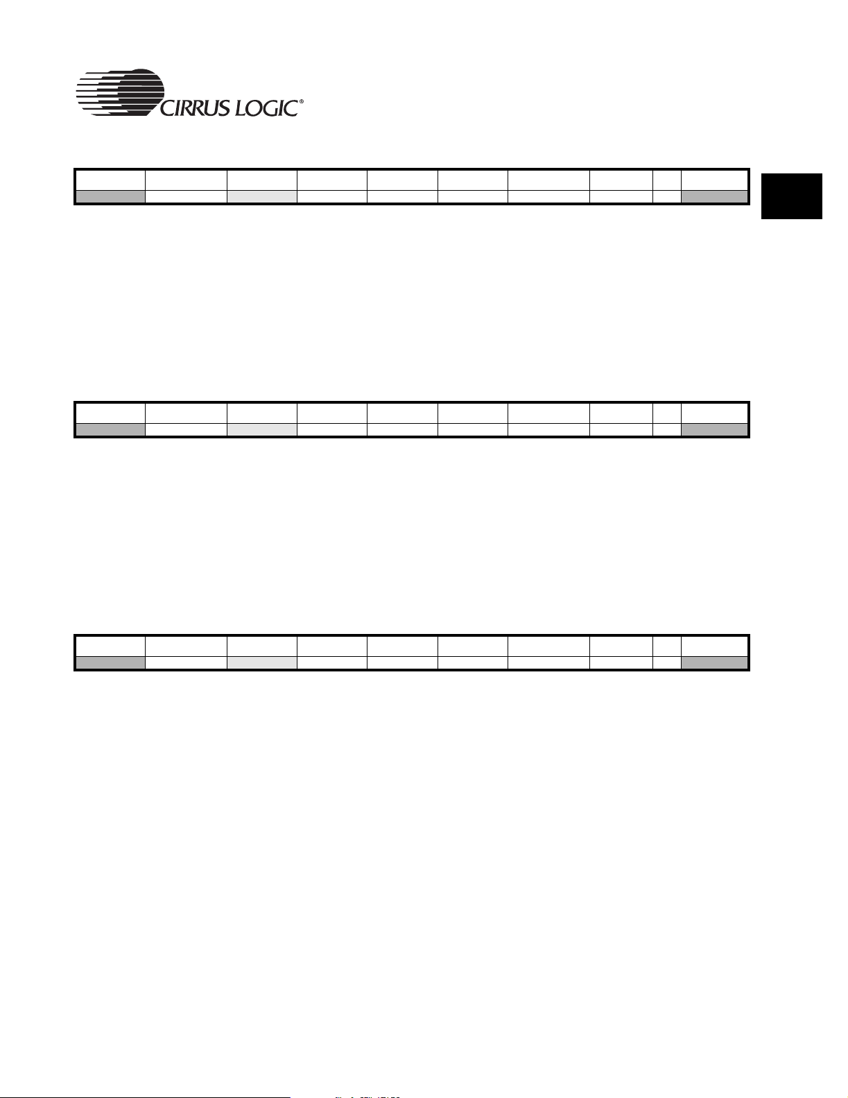
MaverickCrunch Coprocessor
Convert Double Precision Floating Point to 32-bit Integer
31:28 27:24 23:22 21:20 19:16 15:12 11:8 7:5 4 3:0
cond 1 1 1 0 0 0 0 1 CRn CRd 0 1 0 1 1 0 1 0 CRm
Description:
Converts a double precision floating point number to a 32-bit integer.
Mnemonic:
CFCVTD32<cond> CRd, CRn
Bit Definitions:
CRd: Destination register
CRn: Source register
Truncate Single Precision Floating Point to 32-bit Integer
31:28 27:24 23:22 21:20 19:16 15:12 11:8 7:5 4 3:0
cond 1 1 1 0 0 0 0 1 CRn CRd 0 1 0 1 1 1 0 0 CRm
Description:
Truncates a single precision floating point number to a 32-bit integer.
OO
2
Mnemonic:
CFTRUNCS32<cond> CRd, CRn
Bit Definitions:
CRd: Destination register.
CRn: Source register.
Truncate Double Precision Floating Point to 32-bit Integer
31:28 27:24 23:22 21:20 19:16 15:12 11:8 7:5 4 3:0
cond 1 1 1 0 0 0 0 1 CRn CRd 0 1 0 1 1 1 1 0 CRm
Description:
Truncates a double precision floating point number to a 32-bit integer.
Mnemonic:
CFTRUNCD32<cond> CRd, CRn
Bit Definitions:
CRd: Destination register
CRn: Source register
EP9307 User’s Manual - DS667UM1 71
Copyright 2004 Cirrus Logic
Page 72
MaverickCrunch Coprocessor
2.5.5 Shift Instructions
Shift 32-bit Integer
2
31:28 27:24 23:22 21 20 19:16 15:12 11:8 7:5 4 3:0
cond 1 1 1 0 0 0 0 0 CRn Rd 0 1 0 1 0 1 0 1 CRm
Description:
Shifts a 32-bit integer left or right. The shift count is a two’s complement
integer stored in an ARM register; the count is positive for left shifts and
negative for right shifts. This instruction may also be used to copy a 32-bit
integer from one register to another by using a shift value of 0.
Mnemonic:
CFRSHL32<cond> CRm, CRn, Rd
Bit Definitions:
CRm: Destination register
CRn: Source register
Rd: Shift count register in ARM
Shift 64-bit Integer
31:28 27:24 23:22 21 20 19:16 15:12 11:8 7:5 4 3:0
cond 1 1 1 0 0 0 0 0 CRn Rd 0 1 0 1 0 1 1 1 CRm
Definition:
Shifts a 64-bit integer left or right. The shift count is a two’s complement
integer stored in an ARM register; the count is positive for left shifts and
negative for right shifts. This instruction may also be used to copy a 64-bit
integer from one register to another using a shift value of 0.
Mnemonic:
CFRSHL64<cond> CRm, CRn, Rd
Bit Definitions:
CRm: Destination register
CRn: Source register
Rd: Shift count register in ARM
72 EP9307 User’s Manual - DS667UM1
Copyright 2004 Cirrus Logic
Page 73

MaverickCrunch Coprocessor
Shift 32-bit Integer Immediate
31:28 27:24 23:22 21:20 19:16 15:12 11:8 7:5 4 3:0
cond 1 1 1 0 0 0 0 0 CRn CRd 0 1 0 1 Shift[6:4] 0 Shift[3:0]
Definition:
Shift a 32-bit integer by the count specified in the seven bit, two’s complement
immediate value. A positive number indicates a left shift and a negative
number indicates a right shift. This instruction may also be used to copy a 32bit integer from one register to another using a shift value of 0.
Mnemonic:
CFSH32<cond> CRd, CRn, Shift[6:0]
Bit Definitions:
CRd: Destination register
CRn: Source register
Shift[6:0]: Shift count.
Shift 64-bit Integer Immediate
OO
2
31:28 27:24 23:22 21:20 19:16 15:12 11:8 7:5 4 3:0
cond 1 1 1 0 0 0 1 0 CRn CRd 0 1 0 1 Shift[6:4] 0 Shift[3:0]
Definition:
Shifts a 64-bit integer by a count specifies in the seven bit, two’s complement
immediate value. A positive number indicates a left shift and a negative
number indicates a right shift. This instruction may also be used to copy a 64bit integer from one register to another by using a shift value of 0.
Mnemonic:
CFSH64<cond> CRd, CRn, Shift[6:0]
Bit Definitions:
CRd: Destination register
CRn: Source register
Shift[6:0]: Shift count.
EP9307 User’s Manual - DS667UM1 73
Copyright 2004 Cirrus Logic
Page 74

MaverickCrunch Coprocessor
2.5.6 Compare Instructions
Compare Single Precision Floating Point
2
31:28 27:24 23:22 21 20 19:16 15:12 11:8 7:5 4 3:0
cond 1 1 1 0 0 0 0 1 CRn Rd 0 1 0 0 1 0 0 1 CRm
Definition:
Compares two single precision floating point numbers and stores an integer
representing the result in the ARM920T register; the highest four bits of the
integer result match the N, Z, C, and V bits, respectively, in the ARM920T’s
program status register, while the bottom 28 bits are zeros. If Rd = 15, then the
four status bits are stored in the ARM status register, CPSR.
Mnemonic:
CFCMPS<cond> Rd, CRn, CRm
Bit Definitions:
CRn: First source register
CRm: Second source register
Rd: Destination ARM register. If Rd = 15, destination is ARM
N, C, Z, and V flags.
Compare Double Precision Floating Point
31:28 27:24 23:22 21 20 19:16 15:12 11:8 7:5 4 3:0
cond 1 1 1 0 0 0 0 1 CRn Rd 0 1 0 0 1 0 1 1 CRm
Definition:
Compares two double precision floating point numbers and stores an integer
representing the result in the ARM920T register; the highest four bits of the
integer result match the N, Z, C, and V bits, respectively, in the ARM920T’s
program status register, while the bottom 28 bits are zeros. If Rd = 15, then the
four status bits are stored in the ARM status register, CPSR.
Mnemonic:
CFCMPD<cond> Rd, CRn, CRm
Bit Definitions:
CRn: First source register
CRm: Second source register
Rd: Destination ARM register. If Rd = 15, destination is ARM
N, C, Z, and V flags.
74 EP9307 User’s Manual - DS667UM1
Copyright 2004 Cirrus Logic
Page 75

MaverickCrunch Coprocessor
Compare 32-bit Integers
31:28 27:24 23:22 21 20 19:16 15:12 11:8 7:5 4 3:0
cond 1 1 1 0 0 0 0 1 CRn Rd 0 1 0 1 1 0 0 1 CRm
Definition:
Compares two 32-bit integers and stores an integer representing the result in
the ARM920T register; the highest four bits of the integer result match the N,
Z, C, and V bits, respectively, in the ARM920T’s program status register, while
the bottom 28 bits are zeros. If Rd = 15, then the four status bits are stored in
the ARM status register, CPSR.
Mnemonic:
CFCMP32<cond> Rd, CRn, CRm
Bit Definitions:
CRn: First source register
CRm: Second source register
Rd: Destination ARM register. If Rd = 15, destination is ARM
N, C, Z, and V flags.
OO
2
Compare 64-bit Integers
31:28 27:24 23:22 21 20 19:16 15:12 11:8 7:5 4 3:0
cond 1 1 1 0 0 0 0 1 CRn Rd 0 1 0 1 1 0 1 1 CRm
Description:
Compares two 64-bit integers and stores an integer representing the result in
the ARM920T register; the highest four bits of the integer result match the N,
Z, C, and V bits, respectively, in the ARM920T’s program status register, while
the bottom 28 bits are zeros. If Rd = 15, then the four status bits are stored in
the ARM status register, CPSR.
Mnemonic:
CFCMP64<cond> Rd, CRn, CRm
Bit Definitions:
CRn: First source register
CRm: Second source register
Rd: Destination ARM register. If Rd = 15, destination is ARM
N, C, Z, and V flags.
EP9307 User’s Manual - DS667UM1 75
Copyright 2004 Cirrus Logic
Page 76

MaverickCrunch Coprocessor
2.5.7 Floating Point Arithmetic Instructions
Single Precision Floating Point Absolute Value
2
31:28 27:24 23:22 21:20 19:16 15:12 11:8 7:5 4 3:0
cond 1 1 1 0 0 0 1 1 CRn CRd 0 1 0 0 0 0 0 0 CRm
Description:
Computes the absolute value of a single precision floating point number:
CRd = |CRn|
Mnemonic:
CFABSS<cond> CRd, CRn
Bit Definitions:
CRd: Destination register
CRn: Source register
Double Precision Floating Point Absolute Value
31:28 27:24 23:22 21:20 19:16 15:12 11:8 7:5 4 3:0
cond 1 1 1 0 0 0 1 1 CRn CRd 0 1 0 0 0 0 1 0 CRm
Description:
Computes the absolute value of a double precision floating point number.
Mnemonic:
CFABSD<cond> CRd, CRn
Bit Definitions:
CRd: Destination register
CRn: Source register
Single Precision Floating Point Negate
31:28 27:24 23:22 21:20 19:16 15:12 11:8 7:5 4 3:0
cond 1 1 1 0 0 0 1 1 CRn CRd 0 1 0 0 0 1 0 0 CRm
Description:
Takes the negative of a single precision floating point number:
CRd = -CRn
Mnemonic:
CFNEGS<cond> CRd, CRn
Bit Definitions:
CRd: Destination register
CRn: Source register
76 EP9307 User’s Manual - DS667UM1
Copyright 2004 Cirrus Logic
Page 77

MaverickCrunch Coprocessor
Double Precision Floating Point Negate
31:28 27:24 23:22 21:20 19:16 15:12 11:8 7:5 4 3:0
cond 1 1 1 0 0 0 1 1 CRn CRd 0 1 0 0 0 1 1 0 CRm
Description:
Takes the negative of a double precision floating point number.
Mnemonic:
CFNEGD<cond> CRd, CRn
Bit Definitions:
CRd: Destination register
CRn: Source register
Single Precision Floating Point Add
31:28 27:24 23:22 21:20 19:16 15:12 11:8 7:5 4 3:0
cond 1 1 1 0 0 0 1 1 CRn CRd 0 1 0 0 1 0 0 0 CRm
Description:
Adds two single precision floating point numbers:
CRd = CRn + CRm
OO
2
Mnemonic:
CFADDS<cond> CRd, CRn, CRm
Bit Definitions:
CRd: Destination register
CRn: Addend register
CRm: Addend register
Double Precision Floating Point Add
31:28 27:24 23:22 21:20 19:16 15:12 11:8 7:5 4 3:0
cond 1 1 1 0 0 0 1 1 CRn CRd 0 1 0 0 1 0 1 0 CRm
Description:
Adds two double precision floating point numbers.
Mnemonic:
CFADDD<cond> CRd, CRn, CRm
Bit Definitions:
CRd: Destination register
CRn: Addend register
CRm: Addend register
EP9307 User’s Manual - DS667UM1 77
Copyright 2004 Cirrus Logic
Page 78

2
MaverickCrunch Coprocessor
Single Precision Floating Point Subtract
31:28 27:24 23:22 21:20 19:16 15:12 11:8 7:5 4 3:0
cond 1 1 1 0 0 0 1 1 CRn CRd 0 1 0 0 1 1 0 0 CRm
Description:
Subtracts two single precision floating point numbers:
CRd = CRn - CRm
Mnemonic:
CFSUBS<cond> CRd, CRn, CRm
Bit Definitions:
CRd: Destination register
CRn: Minuend register
CRm: Subtrahend register
Double Precision Floating Point Subtract
31:28 27:24 23:22 21:20 19:16 15:12 11:8 7:5 4 3:0
cond 1 1 1 0 0 0 1 1 CRn CRd 0 1 0 0 1 1 1 0 CRm
Description:
Subtracts two double precision floating point numbers.
Mnemonic:
CFSUBD<cond> CRd, CRn, CRm
Bit Definitions:
CRd: Destination register
CRn: Minuend register
CRm: Subtrahend register
Single Precision Floating Point Multiply
31:28 27:24 23:22 21:20 19:16 15:12 11:8 7:5 4 3:0
cond 1 1 1 0 0 0 0 1 CRn CRd 0 1 0 0 0 0 0 0 CRm
Description:
Multiplies two single precision floating point numbers:
CRd = CRn
Mnemonic:
× CRm
CFMULS<cond> CRd, CRn, CRm
Bit Definitions:
CRd: Destination register
CRn: Multiplicand register
CRm: Multiplicand register
78 EP9307 User’s Manual - DS667UM1
Copyright 2004 Cirrus Logic
Page 79

MaverickCrunch Coprocessor
Double Precision Floating Point Multiply
31:28 27:24 23:22 21:20 19:16 15:12 11:8 7:5 4 3:0
cond 1 1 1 0 0 0 0 1 CRn CRd 0 1 0 0 0 0 1 0 CRm
Description:
Multiplies two double precision floating point numbers.
Mnemonic:
CFMULD<cond> CRd, CRn, CRm
Bit Definitions:
CRd: Destination register
CRn: Multiplicand register
CRm: Multiplicand register
OO
2
EP9307 User’s Manual - DS667UM1 79
Copyright 2004 Cirrus Logic
Page 80
MaverickCrunch Coprocessor
2.5.8 Integer Arithmetic Instructions
32-bit Integer Absolute Value
2
31:28 27:24 23:22 21:20 19:16 15:12 11:8 7:5 4 3:0
cond 1 1 1 0 0 0 1 1 CRn CRd 0 1 0 1 0 0 0 0 CRm
Description:
Computes the absolute value of a 32-bit integer.
Mnemonic:
CFABS32<cond> CRd, CRn
Bit Definitions:
CRd: Destination register
CRn: Source register
64-bit Integer Absolute Value
31:28 27:24 23:22 21:20 19:16 15:12 11:8 7:5 4 3:0
cond 1 1 1 0 0 0 1 1 CRn CRd 0 1 0 1 0 0 1 0 CRm
Description:
Computes the absolute value of a 64-bit integer.
Mnemonic:
CFABS64<cond> CRd, CRn
Bit Definitions:
CRd: Destination register
CRn: Source register
32-bit Integer Negate
31:28 27:24 23:22 21:20 19:16 15:12 11:8 7:5 4 3:0
cond 1 1 1 0 0 0 1 1 CRn CRd 0 1 0 1 0 1 0 0 CRm
Description:
Negate a 32-bit integer.
Mnemonic:
CFNEG32<cond> CRd, CRn
Bit Definitions:
CRd: Destination register
CRn: Source register
80 EP9307 User’s Manual - DS667UM1
Copyright 2004 Cirrus Logic
Page 81
MaverickCrunch Coprocessor
64-bit Integer Negate
31:28 27:24 23:22 21:20 19:16 15:12 11:8 7:5 4 3:0
cond 1 1 1 0 0 0 1 1 CRn CRd 0 1 0 1 0 1 1 0 CRm
Description:
Negate a 64-bit integer.
Mnemonic:
CFNEG64<cond> CRd, CRn
Bit Definitions:
CRd: Destination register
CRn: Source register
32-bit Integer Add
31:28 27:24 23:22 21:20 19:16 15:12 11:8 7:5 4 3:0
cond 1 1 1 0 0 0 1 1 CRn CRd 0 1 0 1 1 0 0 0 CRm
Description:
Adds two 32-bit integers.
OO
2
Mnemonic:
CFADD32<cond> CRd, CRn, CRm
Bit Definitions:
CRd: Destination register
CRn: Addend register
CRm: Addend register
64-bit Integer Add
31:28 27:24 23:22 21:20 19:16 15:12 11:8 7:5 4 3:0
cond 1 1 1 0 0 0 1 1 CRn CRd 0 1 0 1 1 0 1 0 CRm
Description:
Adds two 64-bit integers.
Mnemonic:
CFADD64<cond> CRd, CRn, CRm
Bit Definitions:
CRd: Destination register
CRn: Addend register
CRm: Addend register
EP9307 User’s Manual - DS667UM1 81
Copyright 2004 Cirrus Logic
Page 82
2
MaverickCrunch Coprocessor
32-bit Integer Subtract
31:28 27:24 23:22 21:20 19:16 15:12 11:8 7:5 4 3:0
cond 1 1 1 0 0 0 1 1 CRn CRd 0 1 0 1 1 1 0 0 CRm
Description:
Subtracts two 32-bit integers.
Mnemonic:
CFSUB32<cond> CRd, CRn, CRm
Bit Definitions:
CRd: Destination register
CRn: Minuend register
CRm: Subtrahend register
64-bit Integer Subtract
31:28 27:24 23:22 21:20 19:16 15:12 11:8 7:5 4 3:0
cond 1 1 1 0 0 0 1 1 CRn CRd 0 1 0 1 1 1 1 0 CRm
Description:
Subtracts two 64-bit integers.
Mnemonic:
CFSUB64<cond> CRd, CRn, CRm
Bit Definitions:
CRd: Destination register
CRn: Minuend register
CRm: Subtrahend register
32-bit Integer Multiply
31:28 27:24 23:22 21:20 19:16 15:12 11:8 7:5 4 3:0
cond 1 1 1 0 0 0 0 1 CRn CRd 0 1 0 1 0 0 0 0 CRm
Description:
Multiplies two 32-bit integers.
Mnemonic:
CFMUL32<cond> CRd, CRn, CRm
Bit Definitions:
CRd: Destination register
CRn: Multiplicand register
CRm: Multiplicand register
82 EP9307 User’s Manual - DS667UM1
Copyright 2004 Cirrus Logic
Page 83
MaverickCrunch Coprocessor
64-bit Integer Multiply
31:28 27:24 23:22 21:20 19:16 15:12 11:8 7:5 4 3:0
cond 1 1 1 0 0 0 0 1 CRn CRd 0 1 0 1 0 0 1 0 CRm
Description:
Multiplies two 64-bit integers.
Mnemonic:
CFMUL64<cond> CRd, CRn, CRm
Bit Definitions:
CRd: Destination register
CRn: Multiplicand register
CRm: Multiplicand register
32-bit Integer Multiply-Add
31:28 27:24 23:22 21:20 19:16 15:12 11:8 7:5 4 3:0
cond 1 1 1 0 0 0 0 1 CRn CRd 0 1 0 1 0 1 0 0 CRm
OO
2
Description:
Multiplies two 32-bit integers and adds the result to another 32-bit integer:
CRd = CRd + (CRn
Mnemonic:
CFMAC32<cond> CRd, CRn, CRm
Bit Definitions:
CRd: Destination/addend register
CRn: Multiplicand register
CRm: Multiplicand register
32-bit Integer Multiply-Subtract
31:28 27:24 23:22 21:20 19:16 15:12 11:8 7:5 4 3:0
cond 1 1 1 0 0 0 0 1 CRn CRd 0 1 0 1 0 1 1 0 CRm
Description:
Multiplies two 32-bit integers and subtracts the result from another 32-bit
integer:
CRd = CRd - (CRn
Mnemonic:
CFMSC32<cond> CRd, CRn, CRm
× CRm)
× CRm)
Bit Definitions:
CRd: Destination/minuend register
CRn: Multiplicand register
CRm: Multiplicand register
EP9307 User’s Manual - DS667UM1 83
Copyright 2004 Cirrus Logic
Page 84
MaverickCrunch Coprocessor
2.5.9 Accumulator Arithmetic Instructions
32-bit Integer Multiply-Add, Result to Accumulator
2
31:28 27:24 23:22 21:20 19:16 15:12 11:8 7:5 4 3:0
cond 1 1 1 0 0 0 0 0 CRn CRd 0 1 1 0 CRa 0 CRm
Description:
Multiplies two 32-bit integers, adds the product to a third 32-bit integer, and
stores the result in an accumulator:
CRa = CRd + (CRn
Mnemonic:
CFMADD32<cond> CRa, CRd, CRn, CRm
Bit Definitions:
CRa: Destination accumulator
CRd: Addend register
CRn: Multiplicand register
CRm: Multiplicand register
32-bit Integer Multiply-Subtract, Result to Accumulator
31:28 27:24 23:22 21:20 19:16 15:12 11:8 7:5 4 3:0
cond 1 1 1 0 0 0 0 1 CRn CRd 0 1 1 0 CRa 0 CRm
Description:
Multiplies two 32-bit integers, subtracts the product from a third 32-bit integer,
and stores the result in an accumulator:
CRa = CRd - (CRn
× CRm)
× CRm)
Mnemonic:
CFMSUB32<cond> CRa, CRd, CRn, CRm
Bit Definitions:
CRa: Destination accumulator
CRd: Minuend register
CRn: Multiplicand register
CRm: Multiplicand register
84 EP9307 User’s Manual - DS667UM1
Copyright 2004 Cirrus Logic
Page 85
MaverickCrunch Coprocessor
32-bit Integer Multiply-Add to Accumulator
31:28 27:24 23:22 21:20 19:16 15:12 11:8 7:5 4 3:0
cond 1 1 1 0 0 0 1 0 CRn CRd 0 1 1 0 CRa 0 CRm
Description:
Multiplies two 32-bit integers, adds the product to an accumulator, and stores
the result in an accumulator:
CRa = CRd + (CRn
Mnemonic:
CFMADDA32<cond> CRa, CRd, CRn, CRm
Bit Definitions:
CRa: Destination accumulator
CRd: Addend accumulator
CRn: Multiplicand register
CRm: Multiplicand register
× CRm)
OO
2
32-bit Integer Multiply-Subtract from Accumulator
31:28 27:24 23:22 21:20 19:16 15:12 11:8 7:5 4 3:0
cond 1 1 1 0 0 0 1 1 CRn CRd 0 1 1 0 CRa 0 CRm
Description:
Multiplies two 32-bit integers, subtracts the product from an accumulator, and
stores the result in an accumulator:
CRa = CRd - (CRn
Mnemonic:
CFMSUBA32<cond> CRa, CRd, CRn, CRm
Bit Definitions:
CRa: Destination accumulator
CRd: Specifies minuend accumulator
CRn: Multiplicand register
CRm: Multiplicand register
× CRm)
EP9307 User’s Manual - DS667UM1 85
Copyright 2004 Cirrus Logic
Page 86

2
MaverickCrunch Coprocessor
This page intentionally blank.
86 EP9307 User’s Manual - DS667UM1
Copyright 2004 Cirrus Logic
Page 87

3.1 Introduction
The Boot ROM allows a program or OS to boot from the following devices:
• SPI EEPROM
• FLASH/SyncFLASH or SROM/SDRAM
• Serial port
3.1.1 Boot ROM Hardware Operational Overview
PP
Chapter 3
3Boot ROM
3
The Boot ROM is an AHB slave device containing a 16 kbyte maskprogrammed ROM. The AHB slave always operates with one wait state, so all
data reads from the ROM use 2 HCLK cycles.
The ROM contains 3 code sections. The lower 8 kbytes contain the system
boot code. The next 4 kbytes contain the first secure code block, and the top
4 kbytes contain the second secure code block. In non-secure boot, the lower
8 kbytes are accessible. In secure boot, one of the two secure code blocks is
accessible. See Chapter 28, “Security,” for details.
On system reset, the ARM920T begins executing code at address zero. The
system follows the Hardware Configuration controls to select the boot device
that appears at address zero. If Internal Boot is selected, the Boot ROM is
mapped to address zero and the ARM920T will execute the Boot ROM code.
3.1.1.1 Memory Map
The Boot ROM base address (ROM base) is fixed in the EP9307 at
0x8009_0000. It will alias on 16 kbyte intervals. When internal boot is active,
the Boot ROM is double decoded and appears at its normal address space
and at address zero. (The Boot ROM writes the BootModeClr in order to remap
address 0x0 to be external memory while the Boot ROM code continues execution at
0x8009_0000.
)
3.1.2 Boot ROM Software Operational Overview
The Boot ROM is a 16 kbyte mask-programmed ROM that controls the source
of the first off-chip code executed by the EP9307. The code within the Boot
ROM supports the following sources for the EP9307 initialization program:
EP9307 User’s Manual - DS667UM1 87
Copyright 2004 Cirrus Logic
Page 88

Boot ROM
• UART1: Code is downloaded through UART1 into an on chip buffer and
executed.
• SPI Serial ROM: Code is copied from an SPI Serial ROM into an on-chip
buffer and executed.
3
• FLASH: Code present in FLASH memory is executed directly.
Note that the code retrieved via UART1 and the SPI Serial ROM is not
intended to be a complete operating system image. It is intended to be a small
(up to 2 kbyte) loader that will, in turn, retrieve a complete operating system
image. This small loader can retrieve this complete image through UART1 or
the SPI Serial ROM (just as the Boot ROM did) or it can be more sophisticated
and retrieve it through the IrDA, USB, or Ethernet interfaces.
The Boot ROM code disables the ARM920T’s MMU, so any loader program
that is downloaded sees physical addresses. The loader is free to initialize the
page tables and start the MMU and caches if needed.
The Boot ROM code also does not enable interrupts or timers, so that the
system delivered to the user is in a known safe state and is ready for an
operating system or for user code to be loaded.
3.1.2.1 Image Header
One of ASCII strings, “CRUS” or “SURC” must be present as a HeaderID
prefixed to an executable image. This HeaderID must be present in images
copied from the SPI serial ROM and from images programmed into FLASH.
3.1.2.2 Boot Algorithm
Following are the steps in the software boot process:
1. Remap memory.
2. Turn the green LED off and the red LED on.
3. Disable the watchdog.
4. Read the Boot State
5. Set up the Clocks to run from external clocks
6. Based on the Boot State memory width, do the following:
A. initialize the SDRAM and FLASH memory interfaces for slow
(maximum compatibility) operation.
B. Initialize SRAM interfaces for slow operation as well.
C. Perform minimal memory tests.
7. Based on the contents of the SysCfg register, start serial download.
A. Initialize UART1 to 9600 baud, 8 bits, no parity, 1 stop bit.
88 EP9307 User’s Manual - DS667UM1
Copyright 2004 Cirrus Logic
Page 89

Boot ROM
B. Output a “<” character.
C. Read 2048 (decimal count) characters from UART1 and store these
in the internal Boot buffer (alias for the Ethernet Mac buffer)
D. Output a “>” to signify 2048 characters have been read.
PP
E. Turn on Green LED
F. Jump to the start of the internal Boot Buffer.
8. If it is not Serial Download, attempt to read from SPI serial ROM, and then
do the following:
A. Check if the first 4 bytes from the serial ROM are equal to “CRUS” or
to “SURC” in ASCII, verifying the HeaderID.
B. Read the next 2048 (decimal count) bytes into the Internal Boot
Buffer.
C. Turn on Green LED
D. Jump to the start of the Internal Boot Buffer.
9. Attempt to read the “CRUS” or “SURC” HeaderID in ASCII in FLASH
memory at (FLASH Base + 0x0000), verifying the HeaderID. This is read
in for each FLASH Chip select, then do the following:
A. Turn on Green LED
B. Jump to the start of FLASH memory plus four bytes.
10. Attempt to read the “CRUS” or “SURC” HeaderID in ASCII in FLASH
memory at (FLASH Base + 0x1000), verifying the HeaderID. This is read
in for each FLASH Chip select, and then do the following:
3
A. Turn on Green LED
B. Jump to the start of FLASH memory.
11. Attempt to read the “CRUS” or “SURC” HeaderID in ASCII in memory at
0xC000_0000 and 0xF000_0000, verifying the HeaderID. This is read in
for SDRAM or SyncFLASH boot.
A. Turn on Green LED
B. Jump to memory location 0xC000_0004 or 0xF000_0004.
12. Attempt to read the “CRUS” or “SURC” HeaderID in ASCII in memory at
0xC000_1000 and 0xF000_1000, verifying the HeaderID. This is read in
for SDRAM or SyncFLASH boot.
A. Turn on Green LED
B. Jump to memory location 0xC000_0000 or 0xF000_0000 .
13. Copy dummy vectors into low SDRAM
EP9307 User’s Manual - DS667UM1 89
Copyright 2004 Cirrus Logic
Page 90

Boot ROM
3.1.2.3 Flowchart
A. Flash Green LED
Figure 3-1 provides a flow chart for operation of the Boot ROM software.
3
Figure 3-1. Flow Chart of Boot ROM Software
Start Internal Boot
Read Boot
State
UART Download ?
SPI Boot ?
Flash Boot ?
Set Up
Clocks
Download
Code
Copy
Code
Boot Flash
SDCS (6 or 7)
See 4.2.3
Set Up
Memory
Boot
Download
Boot Code
Copy
Sync Boot ?
Copy
Vectors
Flash
Green Led
90 EP9307 User’s Manual - DS667UM1
Boot Sync
SDCS (0 or 3)
See 4.2.4
Copyright 2004 Cirrus Logic
Page 91

3.2 Boot Options
Table 3-1 shows configuration settings that are common to all boot modes.
Table 3-1: Boot Configuration Options (Normal Boot)
Boot ROM
PP
EECLK EEDAT LBOOT1 LBOOT0 ASDO CSn[7:6] Boot Configuration
External boot from Sync memory space selected by
DevCfg3 through the SDRAM Controller. The media
type must be either SROM or SyncFLASH. The
selection of the SRAM width is determined by latched
01 0 0 1
01 0 0 0
11 0 1 x1110
11 0 0 xxx
11 0 0 1
0 0
0 1
1 0
1 1
0 0
0 1
1 0
1 1
01
0 0
0 1
1 0
1 1
CSn[7:6] value:
16-bit SFLASH
16-bit SROM
32-bit SFLASH
32-bit SROM
External boot from Async memory space selected by
nCS0 through Synchronous Memory Controller. The
selection of the SRAM width is determined by latched
CSn[7:6] value:
8-bit SRAM
16-bit SRAM
32-bit SRAM
32-bit SRAM
32-bit serial boot
32-bit serial boot
16-bit serial boot
Internal SPI boot from on-chip ROM, if HeaderID is
found.
Internal boot from on-chip ROM using Synchronous
memory at the chip select where the HeaderID exists.
The selection of the ROM width is determined by
latched CSn[7:6] value:
16-bit
16-bit
32-bit
32-bit
3
Internal boot from on-chip ROM using Asynchronous
memory at the chip select where the HeaderID exists.
The selection of the ROM width is determined by
latched CSn[7:6] value:
8-bit
16-bit
32-bit
32-bit
11 0 0 0
0 0
0 1
1 0
1 1
3.2.1 UART Boot
Make sure that the test pins are configured for internal boot mode. EEDAT
and LBOOT0 should be pulled high and LBOOT1 should be pulled low as
shown in Table 4-1 on page 97. UART 1 is configured at 9600 bps, 8-bits, No
Parity, No flow control. The code performs the following steps:
EP9307 User’s Manual - DS667UM1 91
Copyright 2004 Cirrus Logic
Page 92

Boot ROM
1. A single “<“ is output by UART 1.
2. The “CRUS” or “SURC” HeaderID is read.
3. 2048 characters are received by UART 1 and copied to the Ethernet
buffer at address 0x8001_4000.
3
4. The processor will jump to 0x8001_4000. The processor will be in ARM
SVC mode when the jump occurs.
3.2.2 SPI Boot
To boot from an SPI memory device, make sure that the test pins are
configured for internal boot mode. EEDAT should be pulled high and LBOOT1
and LBOOT0 should be pulled low as shown in Table 4-1 on page 97.
To boot from FLASH, put the “CRUS” or “SURC” HeaderID at the first location
in the SPI memory. The code will be copied from the SPI memory to the
Ethernet buffer at address 0x8001_4000 with a length of 2048 bytes. Code
execution will start at 0x8001_4000 (MAC base + 0x4000). Processor will be
in ARM SVC mode. At this point the user can use the code in the MAC RAM to
load the rest of the SPI memory data.
3.2.3 FLASH Boot
To enable FLASH boot, make sure that the pins are configured for normal boot
mode, as shown in Table 3-1. Also make sure that the FLASH word size is
correct as shown in Table 3-1.
To boot from FLASH, put the “CRUS” or “SURC” HeaderID at one of the
following locations (this location will be referred to as FLASH base + 0x0):
0x1000_0000
0x2000_0000
0x3000_0000
0x6000_0000
0x7000_0000
Code execution will start at address (FLASH base + 0x4). Processor will be in
ARM SVC mode.
Alternatively, to boot from FLASH, put the “CRUS” or “SURC” HeaderID at one
of the following locations (this location will be referred to as FLASH base
+0x1000):
0x1000_1000
0x2000_1000
0x3000_1000
0x6000_0000
0x7000_0000
92 EP9307 User’s Manual - DS667UM1
Copyright 2004 Cirrus Logic
Page 93

Code execution will start at address (FLASH base + 0x0). The processor will
be in ARM SVC mode.
3.2.4 SDRAM or SyncFLASH Boot
Boot ROM
PP
To enable SDRAM or SyncFLASH boot, make sure that the pins are
configured for normal boot mode, as shown in Table 3-1. If booting with
SyncFLASH or a 32-bit SDRAM device, make sure the SDRAM or
SyncFLASH wordsize is correct, as shown in Table 3-1. If booting with a 16-bit
SDRAM device, follow the suggested software sequence of commands, as
shown in Figure 3-2.
Figure 3-2. Flow chart of Boot Sequence for 16-bit SDRAM Devices
Boot Internally with Asynchronous Device
Re-configure SDRAM for 16-bit access
Branch to desired SDRAM memory
To boot from SDRAM or SyncFLASH, put the “CRUS” or “SURC” HeaderID at
one of the following locations (this location is Base + 0x0):
0xC000_0000
0xF000_0000
Code execution will start at address (Base + 0x4). Processor will be in ARM
SVC mode.
3
Alternatively, to boot from SDRAM or SyncFLASH, put the “CRUS” or “SURC”
HeaderID at one of the following locations (this is Base + 0x1000):
0xC000_1000
0xF000_1000
Code execution will start at address (Base + 0x0). The processor will be in
ARM SVC mode.
3.2.5 Synchronous Memory Operation
If running from Synchronous memory, before issuing a software reset, perform
the following procedure:
1. Run from SDRAM.
2. Perform a software reset (because of the SWRST bit in DEVCFG).
3. Run the internal boot code and boot to FLASH.
EP9307 User’s Manual - DS667UM1 93
Copyright 2004 Cirrus Logic
Page 94

3
Boot ROM
4. Set the PLL back to use the external clock.
5. Set up the SDRAM.
6. Load the programs to SDRAM.
7. Run from SDRAM.
94 EP9307 User’s Manual - DS667UM1
Copyright 2004 Cirrus Logic
Page 95

Chapter 4
4System Controller
QQ
4.1 Introduction
The System Controller (Syscon) provides the EP9307 central clock and
control resources. These central resources are:
• Clock control
• Power management
• System configuration management.
These resources are controlled by a set of software-locked registers which
can be used to prevent accidental accesses. Syscon generates the various
bus and peripheral clocks as well as controls the system startup configuration.
4.1.1 System Startup
System startup begins with the assertion of a reset signal. There are five
different categories of reset events in the device. In order of decreasing effect,
the reset events are:
• PRSTn (external pin for power-on reset)
• RSTOn (external pin for user reset)
• Three-key reset (externally generated, behaves like user reset)
4
• Watchdog reset (internally generated)
• Software reset (internally generated)
During the time that any reset is active, the system is halted until it exits the
reset state.
When the device starts with an external PRSTn or RSTOn, certain hardware
configurations are determined, and some system configuration information will
be recorded so that software can access it. See the details in “System Reset”
on page 95 and “Hardware Configuration Control” on page 96.
4.1.2 System Reset
The device system reset consists of several events and signals. It has four
levels of reset control. They are:
EP9307 User’s Manual - DS667UM1 95
Copyright 2004 Cirrus Logic
Page 96

System Controller
• Power-on-reset, controlled by PRSTn pin. It resets the entire chip with no
exceptions.
• User reset, controlled by RSTOn pin. While active, it resets the entire
chip, except certain system variables such as RTC, SDRAM refresh
control/global configuration, and the registers in the Syscon.
Note: If PLLs are enabled, user reset does NOT disable or reset the PLLs. They retain
their frequency settings.
4
• Three-key reset. When F2, F4, and F7 are pressed, a user reset (above)
occurs.
• Software reset and watchdog reset. They perform the functions of the
user reset (above), but are under software control.
Watchdog and PwrSts registers contain the information regarding which reset
event occurred. Note that only the Watchdog timer contains information about
a user-generated 3-key reset.
4.1.3 Hardware Configuration Control
The Hardware Configuration controls provide a mechanism to place the
system into various boot configurations. In addition, one of several external
boot memory options can be selected at system wake up.
The Hardware Configuration controls are defined by a set of device pins that
are latched into configuration control bits on the assertion of chip reset on the
rising edge of the PRSTn or RSTOn pin. The different hardware configuration
bits define watchdog behavior, boot mode (internal or external), boot
synchronicity, and external boot width. The latched pins are:
CSn[1] - Disable Watchdog reset timer
CSn[2] - Disable Watchdog reset duration
CSn[3] - Should be pulled up to “1”
EECLK - Select internal or external boot
EEDAT - Should be pulled upto “1”
BOOT[1:0] - Select boot mode
ASDO - Select synchronous or asynchronous boot
CSn[7:6] - Select external boot width
The latched version of these signals have an “L” prefix, and are readable by
software in the SysCfg register. Note that the signals EECLK and EEDAT may
have 1 kΩ pull-ups if used in an open-drain two-wire serial port application.
(The default state assignments will assume this pull-up.)
The Hardware Control configurations are as show in Table 4-1.
The normal boot function is described in Chapter 3, Boot ROM.
96 EP9307 User’s Manual - DS667UM1
Copyright 2004 Cirrus Logic
Page 97
System Controller
Serial boot is functionally identical to normal boot except that the SBoot bit in
the SysCfg register is set. This mode is available for a software configuration
option that is readable by the boot code.
In either normal boot or serial boot mode, once the chip starts up, it will begin
to execute the instruction at logical address 0x0000_0000. Various
configuration options are provided to select the different memory elements for
booting from location 0. The options are listed in Table 4-1.
QQ
Table 4-1: Boot Configuration Options
EECLK EEDAT LBOOT1 LBOOT0 ASDO CSn[7:6] Boot Configuration
01 0 0 1
01 0 0 0
11 0 1 x1110
11 0 0 xxx
0 0
0 1
1 0
1 1
0 0
0 1
1 0
1 1
01
4
External boot from Sync memory space selected by
DevCfg3 through the SDRAM Controller. The media
type must be either SROM or SyncFLASH. The
selection of the SRAM width is determined by latched
CSn[7:6] value:
16-bit SFLASH
16-bit SROM
32-bit SFLASH
32-bit SROM
External boot from Async memory space selected by
nCS0 through Synchronous Memory Controller. The
selection of the SRAM width is determined by latched
CSn[7:6] value:
8-bit SRAM
16-bit SRAM
32-bit SRAM
32-bit SRAM
32-bit serial boot
32-bit serial boot
16-bit serial boot
Internal SPI boot from on-chip ROM, if HeaderID is
found.
Internal boot from on-chip ROM using Synchronous
memory at the chip select where the HeaderID exists.
The selection of the ROM width is determined by
latched CSn[7:6] value:
0 0
11 0 0 1
11 0 0 0
EP9307 User’s Manual - DS667UM1 97
Copyright 2004 Cirrus Logic
0 1
1 0
1 1
0 0
0 1
1 0
1 1
16-bit
16-bit
32-bit
32-bit
Internal boot from on-chip ROM using Asynchronous
memory at the chip select where the HeaderID exists.
The selection of the ROM width is determined by
latched CSn[7:6] value:
8-bit
16-bit
32-bit
32-bit
Page 98

4
System Controller
4.1.4 Software System Configuration Options
There are several system configuration options selectable by the DeviceCfg
and SysCfg registers. These registers provide the selection of several pin
multiplexing options and also provide software access to the system reset
configuration options. Please refer to the descriptions of the registers,
“DeviceCfg” on page 120 and “SysCfg” on page 128, for a detailed
explanation.
4.1.5 Clock Control
The device uses a flexible system to generate the required clocks. The goal of
the clock system is to generate as many as 20 independent clock frequencies,
some with very tight accuracy requirements, all from a single external lowfrequency crystal or other external clock source. The system was designed so
that once it has been configured, the processor speed, bus speeds, and video
clocks can be set to a number of different speeds without affecting the speeds
of the other clocks in the system.
4.1.5.1 Oscillators and Programmable PLLs
The device has an interface to two external crystal oscillators with the
frequency of 32 KHz and 14.7456 MHz. To generate the required highfrequency clocks, the system uses two phase-locked-loops (PLLs) to multiply
the incoming 14.7456 MHz low frequency signal to much higher frequencies
(up to about 400 MHz) that are then divided down by programmable dividers
to produce the needed clocks. The PLLs operate independently of one
another.
The system is split into two “trunks”, each of which is driven by one of the
PLLs. The processor and bus clocks are derived from trunk 1 (PLL1). The
USB and FIR clocks are derived from trunk 2 (PLL2). Other low-frequency
clocks are divided from the original crystal frequency. The MIR, audio, and
video clocks can be independently sourced from either trunk. Figure 4-1,
below, shows the PLL1 structure used in the EP9307. Since PLL2 is identical
to PLL1, wherever the phrase of “PLL1” is used in the figure, it applies to PLL2
as well.
98 EP9307 User’s Manual - DS667UM1
Copyright 2004 Cirrus Logic
Page 99
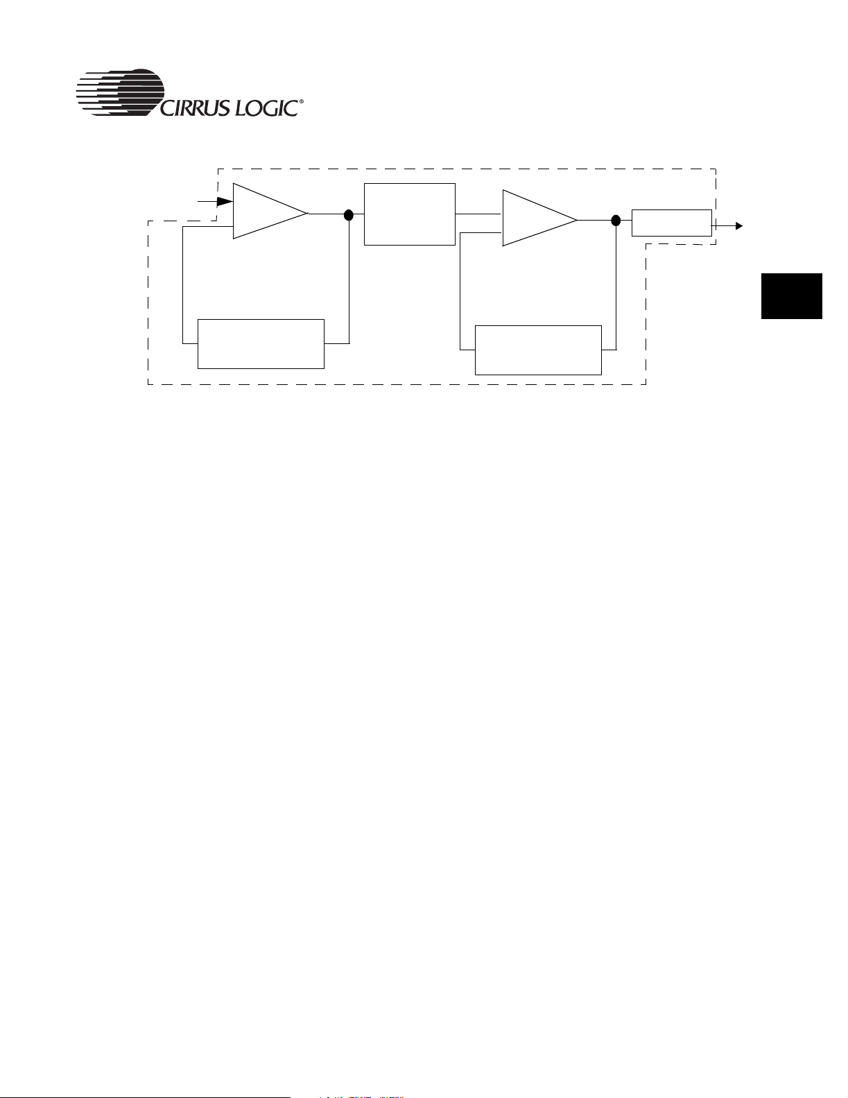
Figure 4-1. Phase Locked Loop (PLL) Structure
System Controller
QQ
14.7456
MHz
PLL1_X1
Feedback Divider
PLL1_X1FBD
Both PLLs are software programmable (each value is defined in ClkSet1 and
ClkSet2 registers respectively). The frequency of output clock Fout shows in
the next equation:
Fout 14.7456M Hz
Here PLL1_X1FBD, PLL1_X2FBD, PLL1_X2IPD and PLL1_PS are the bit
fields in ClkSet1 register. The user must be aware of the requirements of PLL
operation. They are:
Input Divider
PLL1_X2IPD
PLL1_X1FBD 1+()PLL1_X2FBD 1+()×
------- ------------- ------------ ------------- ------------ ------------- --------- ------------ ------------- --
⋅=
PLL1_X2
Feedback Divider
PLL1_X2FBD
PLL1_X2IPD 1+()2
×
2^(PLL1_PS)
PLL1_PS
Fout
4
• PLL1_X1 desired reference clock frequency range is > 11.058 MHz and <
200 MHz
• PLL1_X1 output frequency range is > 294 MHz and < 368 MHz
• PLL1_X2 desired reference clock frequency (after PLL1_X2IPD divider) is
> 12.9 MHz and < 200 MHz.
• PLL1_X2 output, BEFORE the PS divide, must be > 290 MHz and <=
528 MHz
Again, the same conditions are applied to PLL2 as well.
4.1.5.2 Bus and Peripheral Clock Generation
Figure 4-2 illustrates the clock generation system.
EP9307 User’s Manual - DS667UM1 99
Copyright 2004 Cirrus Logic
Page 100
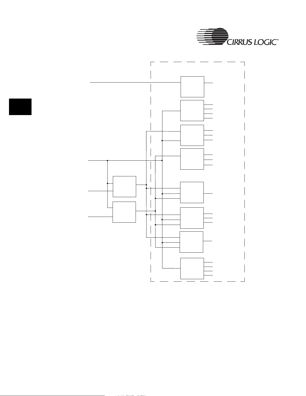
System Controller
Figure 4-2. EP9307 Clock Generation System
Syscon
4
32 KHz Oscillator
14.7456 MHz Oscillator
PLL1 CFG
PLL2 CFG
PLL1
PLL2
32 KHz
Divide
Peripheral
Clocks
CPU an d
Bus Clocks
USB an d
FIR Clocks
Vi de o
Clocks
CPU and
Audi o
Bus Clocks
Clocks
WAT C H _ C L K
UARTxCLK
SSPCLK
PWMCLK
Timer Clocks
FCLK
HCLK
PCLK
USBHost48MHz
USBHost12MHz
FIR_ CLK
VCLK
SCLK
LRCLK
MCLK
MIR
Clock
Key
Tou ch
Clock
MIR_CLK
KEY_CLK
TOUCH_ CLK
ADC_CLK
FILT_CLK
4.1.5.2.1 Bus Clock Generation
Figure 4-3 shows the flow of generated system bus clocks, including the ARM
processor clock (FCLK), the AHB bus clock (HCLK), and the APB bus clock
(PCLK).
100 EP9307 User’s Manual - DS667UM1
Copyright 2004 Cirrus Logic
 Loading...