

Page 1

EP9301 User’s Guide
http://www.cirrus.com
Release 1.00
Copyright © Cirrus Logic, Inc. 2004
(All Rights Reserved)
FEB ‘04
DS636UM2
Page 2

Revision Date Changes
1 12 December 2003 Initial Release
2 12 February 2004
Updated ChipID, SysCfg and DeviceCfg register information.
Added ExtensionID register information to the Security section.
Contacting Cirrus Logic Support
For all product questions and inquiries contact a Cirrus Logic Sales Representative.
To find one nearest you go to www.cirrus.com
IMPORTANT NOTICE
Cirrus Logic, Inc. and i ts subsidiaries (“Ci rrus”) beli eve that the informati on contai ned in this document is accurate and reli able. However, the information is
subject to change without notice and is provided “AS IS” without warranty of any kind (express or implied). Customers are advised to obtain the latest version
of relevant information to verify, before placing orders, that information being relied on is current and complete. All products are sold subject to the terms and
conditions of sale supplied at the ti me of order acknowledgment, including those pertaini ng to warranty, patent infringement, and limitation of li ability. No responsibility i s assumed by Cirrus for the use of this information, incl uding use of this informati on as the basis for manufacture or sale of any items, or for i nfringement of patents or other rights of third parties. This document is the property of Cirrus and by furnishing this information, Cirrus grants no license, express
or implied under any patents, mask work rights , copyrights, trademarks, trade secret s or other int ellectual pr operty right s. Cirrus owns the copyrights associated
with the informati on contained herein and gives consent for copies to be made of the information only for use within your organi zation with respect to Cirrus
integrated circui ts or other products of Cirrus. This consent does not extend to other copying such as copying for general distribution, adverti sing or promotional
purposes, or for creating any work for resale.
CERTAIN APPLICATIONS USI NG SEMI CONDUCTOR PRODUCTS MAY INVOLVE POTENTIAL RISKS OF DEATH, PERSONAL INJURY, OR SEVERE
PROPERTY OR ENVIRONMENTAL DAMAGE (“CRITICAL APPLICATIONS”). CIRRUS PRODUCTS ARE NOT DESIGNED, AUTHORIZED OR WARRANTED FOR USE IN AIRCRAFT SYSTEMS, MILITARY APPLICATIONS, PRODUCTS SURGICALLY IMPLANTED INTO THE BODY, LIFE SUPPORT PRODUCTS OR OTHER CRITICAL APPLICATIONS ( INCLUDING MEDICAL DEVICES, AIRCRAFT SYSTEMS OR COMPONENTS AND PERSONAL OR
AUTOMOTIVE SAFETY OR SECURITY DEVICES). I NCLUSION OF CIRRUS PRODUCTS IN SUCH APPLICATIONS IS UNDERSTOOD TO BE FULLY AT
THE CUSTOMER’ S RISK AND CIRRUS DISCLAIMS AND MAKES NO WARRANTY, EXPRESS, STATUTORY OR IMPLIED, I NCLUDI NG THE I MPLIED
WARRANTIES OF MERCHANTABILITY AND FITNESS FOR PARTICULAR PURPOSE, WITH REGARD TO ANY CIRRUS PRODUCT THAT IS USED IN
SUCH A MANNER. IF THE CUSTOMER OR CUSTOMER’S CUSTOMER USES OR PERMITS THE USE OF CIRRUS PRODUCTS IN CRITICAL APPLICATIONS, CUSTOMER AGREES, BY SUCH USE, TO FULLY INDEMNIFY CIRRUS, ITS OFFICERS, DIRECTORS, EMPLOYEES, DISTRIBUTORS AND OTHER AGENTS FROM ANY AND ALL LIABILITY, INCLUDING ATTORNEYS’ FEES AND COSTS, THAT MAY RESULT FROM OR ARISE IN CONNECTION
WITH THESE USES.
Cirrus Logi c, Cirrus, MaverickKey, and the Cirrus Logic logo de signs are trademarks of Cirrus Logic, I nc. All other brand and product names in thi s document
may be trademarks or service marks of their respective owners.
Microsoft and Windows are registered trademarks of Microsoft Corporation.
Microwire is a trademark of National Semiconductor Corp. National Semiconductor is a registered trad emark of National Semiconductor Corp.
Texas Instruments is a registered trademark of Texas Instruments, Inc.
Motorola is a registered trademark of Motorola, Inc.
LINUX is a registered trademark of Linus Torval ds.
2 EP9301 User’s Manual - DS636UM2
Copyright 2004 Cirrus Logic
Page 3

About the EP9301 User’s Guide
This Guide describes the architecture, hardware and operation of the Cirrus
Logic EP9301. It is intended to be used in conjunction with the EP9301
Datasheet, which contains the full electrical specifications for the device.
How to Use this Guide
Subject Matter Location
AC’97 Chapter 18 - AC’97 Controller
ARM920T Processor
Boot ROM, Hardware and Software Chapter 3 - Boot ROM
Booting From SROM or SyncFlash Chapter 10 - SDRAM, SyncROM, and SyncFLASH Controller
Buses - AMBA, AHB, APB
DMA Controller Chapter 7 - DMA Controller
EP9301 Block Diagram
Ethernet Chapter 6 - 1/10/100 Mbps Ethernet LAN Controller
GPIO Chapter 21 - GPIO Interface
HDLC Chapter 11 - UART1 With HDLC and Modem Control Signals
2
I
S Chapter 17 - I2S Controller
Infra-Red Interface Chapter 13 - IrDA
Interrupt Registers Chapter 5 - Vectored Interrupt Controller
Interrupts Chapter 5 - Vectored Interrupt Controller
IrDA Chapter 13 - IrDA
MAC Chapter 6 - 1/10/100 Mbps Ethernet LAN Controller
Memory Map Chapter 1 - Introduction
Modem Chapter 11 - UART1 With HDLC and Modem Control Signals
Power Management Chapter 4 - System Controller
Programming Clocks Chapter 4 - System Controller
Real Time Clock Chapter 16 - Real Time Clock With Software Trim
Register List Chapter 1 - Introduction
Chapter 2 - ARM920T Core and Advanced High-Speed Bus
(AHB)
Chapter 2 - ARM920T Core and Advanced High-Speed Bus
(AHB)
Chapter 2 - ARM920T Core and Advanced High-Speed Bus
(AHB)
Preface
EP9301 User’s Manual - DS636UM2 3
Copyright 2004 Cirrus Logic
Page 4

Subject Matter Location
RTC Chapter 16 - Real Time Clock With Software Trim
SDRAM Chapter 10 - SDRAM, SyncROM, and SyncFLASH Controller
Security Chapter 22 - Security
SMC Chapter 9 - Static Memory Controller
SSP Chapter 19 - Synchronous Serial Port
Static Memory Controller Chapter 9 - Static Memory Controller
System Configuration Chapter 4 - System Controller
System Registers Chapter 4 - System Controller
Timers Chapter 14 - Timers
Touch Screen Chapter 20 - Analog-to-Digital Converter (ADC) Interface
UART
USB Chapter 8 - Universal Serial Bus Host Controller
Vectored Interrupt Registers Chapter 5 - Vectored Interrupt Controller
Vectored Interrupts Chapter 5 - Vectored Interrupt Controller
Watchdog Timer Chapter 15 - Watchdog Timer
Chapter 11 - UART1 With HDLC and Modem Control Signals
Chapter 12 - UART2
Related Documents from Cirrus Logic
1. EP9301 Datasheet, document number - DS636PP1
Reference Documents
1. ARM920T Technical Reference Manual
2. AMBA Specification (Rev. 2.0), ARM IHI 0011A, ARM Limited.
3. AHB Example AMBA System (Addendum 01), ARM DDI 0170A, ARM
Limited.
4. The coprocessor instruction assembler notation can be referenced from
ARM programming manuals or the Quick Reference Card, document
number ARM QRC 0001D.
5. The MAC engine is compliant with the requirements of ISO/IEC 8802-3
(1993), Sections 3 and 4.
6. OpenHCI - Open Host Controller interface Specification for USB, Release
1.0a; Compaq, Microsoft, National Semiconductor.
7. ARM Coprocessor Quick Reference Card, document number ARM QRC
0001D.
4 EP9301 User’s Manual - DS636UM2
Copyright 2004 Cirrus Logic
Page 5

8. Information Technology, AT Attachment with Packet Interface - 5
(ATA/ATAPI-5) ANSI NCITS document T13 1321D, Revision 3, 29
February 2000
9. OpenHCI - Open Host Controller Interface Specification for USB,
Release: 1.0a, Released - 09/14/99 2:33 PM
10. ARM PrimeCell PL190-Rel1v1 Revision 1.7 Technical Reference Manual
DDI0181C
11. Audio Codec ‘97, Revision 2.3, April 2002, Intel Corporation
Notational Conventions
This document uses the following conventions:
• Internal and external Signal Names, and Pin Names use mixed upper and
lower case alphanumeric, and are shown in bold font: RDLED.
• Register Bit Fields are named using upper and lower case alphanumeric:
that is, SBOOT, LCSn1.
• Registers are named using mixed upper and lower case alphanumeric:
that is, SysCfg or PxDDR. (Where there are multiple registers with similar
names, a lower case “x” is used as a place holder. For example, in the
PxDDR registers, x represents a letter between A and H, indicating the
specific port being discussed.)
Caution: In the Internal Register Map in Table 2-7 on page 7-47, some
memory locations are listed as Reserved. These memory
locations should not be used. Reading from these memory
locations will yield invalid data. Writing to these memory locations
may cause unpredictable results.
(An example register description is shown below. This description is used for
the following examples.)
A specific bit may be specified in one of two ways:
register name[bit number]: SysCfg[29]
By
or by
register name.bit field[bit number]: SysCfg.REV[1]
Both of these representations refer to the same bit.
The following:
SysCfg[8]
, or
,
SysCfg.SBOOT
also refer to the same bit.
Hexidecimal numbers are referred to as
0x0000_0000
.
EP9301 User’s Manual - DS636UM2 5
Copyright 2004 Cirrus Logic
Page 6
Binary numbers are referred to as
0000_0000b
.
Register Example
Note: This is only and example. For actual SysCfg register information, see “SysCfg”
on page 97.
SysCfg
31 30 29 28 27 26 25 24 23 22 21 20 19 18 17 16
REV RSVD
15 14 13 12 11 10 9 8 7 6 5 4 3 2 1 0
RSVD SBOOT LCSn7 LCSn6 LASDO LEEDA LEECLK RSVD LCSn2 LCSn1
Address:
0x8093_009C - Read/Write, Software locked
Default:
0x0000_0000
Definition:
System Configuration Register. Provides various system configuration
options.
Bit Descriptions:
RSVD: Reserved. Unknown During Read.
REV: Revision, reads chip Version number: 0 - Rev A, 1 - Rev B,
2 - Rev C, 3 - Rev D.
SBOOT: Serial Boot Flag. This bit is read-only.
1 hardware detected Serial Boot selection,
0 hardware detected Normal Boot.
LCSn7, LCSn6: Latched version of CSn7 and CSn6 respectively. These
are used to define the external bus width for the boot code
boot.
LASDO: Latched version of ASDO pin. Used to select synchronous
versus asynchronous boot device.
LEEDA: Latched version of EEDAT pin.
LEECLK: Define Internal or external boot:
1 Internal
0 External
6 EP9301 User’s Manual - DS636UM2
Copyright 2004 Cirrus Logic
Page 7

LCSn2, LCSn1: Define Watchdog startup action:
0 0 Watchdog disabled, Reset duration disabled
0 1 Watchdog disabled, Reset duration active
1 0 Watchdog active, Reset duration disabled
1 1 Watchdog active, Reset duration active
EP9301 User’s Manual - DS636UM2 7
Copyright 2004 Cirrus Logic
Page 8

This page intentionally blank.
8 EP9301 User’s Manual - DS636UM2
Copyright 2004 Cirrus Logic
Page 9

Table of Contents
Preface............................................................................................................. 3
About the EP9301 User’s Guide ............................................................................................................ 3
How to Use this Guide ...........................................................................................................................3
Related Documents from Cirrus Logic ...................................................................................................4
Reference Documents ...........................................................................................................................4
Notational Conventions ..........................................................................................................................5
Chapter 1 Introduction ............................................................................... 23
1.1 Introduction ...................................................................................................................................23
1.2 EP9301 Features ..........................................................................................................................23
1.3 EP9301 Applications .....................................................................................................................25
1.4 Overview of EP9301 Features ......................................................................................................25
1.4.1 High-Performance ARM920T Processor Core ....................................................................25
1.4.2 MaverickKey™ Unique ID Secures Digital Content and OEM Designs ..............................26
1.4.3 Integrated Two-port USB 2.0 Full Speed Host with Transceivers .......................................26
1.4.4 Integrated Ethernet MAC Reduces BOM Costs ..................................................................26
1.4.5 Multiple Booting Mechanisms Increase Flexibility ...............................................................26
1.4.6 Abundant General Purpose I/Os Build Flexible Systems ....................................................27
1.4.7 General-Purpose Memory Interface (SDRAM, SRAM, ROM and FLASH) .........................27
1.4.8 12-Bit Analog-to-Digital Converter (ADC) Functionality....................................................... 27
Chapter 2 ARM920T Core and Advanced High-Speed Bus (AHB) ......... 29
2.1 Introduction ...................................................................................................................................29
2.2 Overview: ARM920T Processor Core ...........................................................................................29
2.2.1 Features ..............................................................................................................................29
2.2.2 Block Diagram .....................................................................................................................30
2.2.3 Operations...........................................................................................................................30
2.2.3.1 ARM9TDMI Core........................................................................................................31
2.2.3.2 Memory Management Unit .........................................................................................32
2.2.3.3 Cache and Write Buffer..............................................................................................33
2.2.4 AMBA AHB Bus Interface Overview....................................................................................34
2.2.5 EP9301 AHB Implementation Details..................................................................................36
2.2.6 Memory and Bus Access Errors ..........................................................................................37
2.2.7 Bus Arbitration .....................................................................................................................37
2.2.7.1 Main AHB Bus Arbiter ................................................................................................38
2.2.7.2 EBI Bus Arbiter...........................................................................................................39
2.3 AHB Decoder ................................................................................................................................39
2.3.1 AHB Bus Slave ....................................................................................................................40
2.3.2 AHB to APB Bridge..............................................................................................................40
2.3.2.1 Function and Operation of APB Bridge......................................................................41
2.3.3 APB Bus Slave ....................................................................................................................41
2.3.4 Register Definitions .............................................................................................................42
2.3.5 Memory Map........................................................................................................................45
2.3.6 Internal Register Map ..........................................................................................................46
2.3.6.1 Memory Access Rules ...............................................................................................46
Chapter 3 Boot ROM .................................................................................. 59
3.1 Introduction ...................................................................................................................................59
EP9301 User’s Manual - DS636UM2 9
Copyright 2004 Cirrus Logic
Page 10

3.1.1 Boot ROM Hardware Operational Overview ....................................................................... 59
3.1.1.1 Memory Map.............................................................................................................. 59
3.1.2 Boot ROM Software Operational Overview......................................................................... 59
3.1.2.1 Image Header ............................................................................................................ 60
3.1.2.2 Boot Algorithm ........................................................................................................... 60
3.1.2.3 Flowchart................................................................................................................... 62
3.2 Boot Options................................................................................................................................. 62
3.2.1 UART Boot.......................................................................................................................... 63
3.2.2 SPI Boot.............................................................................................................................. 63
3.2.3 FLASH Boot ........................................................................................................................ 64
3.2.4 SDRAM or SyncFLASH Boot.............................................................................................. 64
3.2.5 Synchronous Memory Operation ........................................................................................ 65
Chapter 4 System Controller .....................................................................67
4.1 Introduction ................................................................................................................................... 67
4.1.1 System Startup.................................................................................................................... 67
4.1.2 System Reset...................................................................................................................... 67
4.1.3 Hardware Configuration Control.......................................................................................... 68
4.1.4 Software System Configuration Options ............................................................................. 69
4.1.5 Clock Control....................................................................................................................... 69
4.1.5.1 Oscillators and Programmable PLLs ......................................................................... 70
4.1.5.2 Bus and Peripheral Clock Generation ....................................................................... 71
4.1.5.3 Steps for Clock Configuration.................................................................................... 74
4.1.6 Power Management ............................................................................................................ 75
4.1.6.1 Clock Gatings ............................................................................................................ 75
4.1.6.2 System Power States ................................................................................................ 75
4.1.7 Interrupt Generation ............................................................................................................ 77
4.2 Registers ...................................................................................................................................... 79
Chapter 5 Vectored Interrupt Controller ................................................... 99
5.1 Introduction ................................................................................................................................... 99
5.1.1 Interrupt Priority................................................................................................................. 100
5.1.2 Interrupt Descriptions ........................................................................................................ 102
5.2 Registers .................................................................................................................................... 106
Chapter 6 1/10/100 Mbps Ethernet LAN Controller ................................ 119
6.1 Introduction ................................................................................................................................. 119
6.1.1 Detailed Description.......................................................................................................... 119
6.1.1.1 Host Interface and Descriptor Processor................................................................. 119
6.1.1.2 Reset and Initialization ............................................................................................ 120
6.1.1.3 Powerdown Modes .................................................................................................. 120
6.1.1.4 Address Space ........................................................................................................ 121
6.1.2 MAC Engine...................................................................................................................... 121
6.1.2.1 Data Encapsulation ................................................................................................. 121
6.1.3 Packet Transmission Process........................................................................................... 122
6.1.3.1 Carrier Deference .................................................................................................... 123
6.1.4 Transmit Back-Off ............................................................................................................. 125
6.1.4.1 Transmission ...........................................................................................................125
10 EP9301 User’s Manual - DS636UM2
Copyright 2004 Cirrus Logic
Page 11

6.1.4.2 The FCS Field..........................................................................................................126
6.1.4.3 Bit Order...................................................................................................................126
6.1.4.4 Destination Address (DA) Filter................................................................................126
6.1.4.5 Perfect Address Filtering..........................................................................................126
6.1.4.6 Hash Filter................................................................................................................127
6.1.4.7 Flow Control .............................................................................................................128
6.1.4.8 Receive Flow Control...............................................................................................128
6.1.4.9 Transmit Flow Control ..............................................................................................129
6.1.4.10 Rx Missed and Tx Collision Counters....................................................................129
6.1.4.11 Accessing the MII...................................................................................................130
6.2 Descriptor Processor...................................................................................................................131
6.2.1 Receive Descriptor Processor Queues .............................................................................131
6.2.2 Receive Descriptor Queue ................................................................................................132
6.2.3 Receive Status Queue.......................................................................................................134
6.2.3.1 Receive Status Format.............................................................................................137
6.2.3.2 Receive Flow............................................................................................................140
6.2.3.3 Receive Errors .........................................................................................................141
6.2.3.4 Receive Descriptor Data/Status Flow ......................................................................142
6.2.3.5 Receive Descriptor Example....................................................................................143
6.2.3.6 Receive Frame Pre-Processing ...............................................................................143
6.2.3.7 Transmit Descriptor Processor.................................................................................144
6.2.3.8 Transmit Descriptor Queue ......................................................................................144
6.2.3.9 Transmit Descriptor Format .....................................................................................147
6.2.3.10 Transmit Status Queue ..........................................................................................148
6.2.3.11 Transmit Status Format..........................................................................................150
6.2.3.12 Transmit Flow.........................................................................................................152
6.2.3.13 Transmit Errors ......................................................................................................153
6.2.3.14 Transmit Descriptor Data/Status Flow ...................................................................154
6.2.4 Interrupts ...........................................................................................................................155
6.2.4.1 Interrupt Processing.................................................................................................155
6.2.5 Initialization........................................................................................................................155
6.2.5.1 Interrupt Processing.................................................................................................156
6.2.5.2 Receive Queue Processing......................................................................................156
6.2.5.3 Transmit Queue Processing.....................................................................................156
6.2.5.4 Other Processing .....................................................................................................157
6.2.5.5 Transmit Restart Process.........................................................................................157
6.3 Registers.....................................................................................................................................159
Chapter 7 DMA Controller........................................................................ 213
7.1 Introduction .................................................................................................................................213
7.1.1 DMA Features List.............................................................................................................213
7.1.2 Managing Data Transfers Using a DMA Channel .............................................................214
7.1.3 DMA Operations ................................................................................................................215
7.1.3.1 Memory-to-Memory Channels..................................................................................216
7.1.3.2 Memory-to-Peripheral Channels ..............................................................................216
7.1.4 Internal M2P or P2M AHB Master Interface Functional Description..................................217
7.1.5 M2M AHB Master Interface Functional Description...........................................................218
EP9301 User’s Manual - DS636UM2 11
Copyright 2004 Cirrus Logic
Page 12

7.1.5.1 Software Trigger Mode ............................................................................................ 218
7.1.5.2 Hardware Trigger Mode for Internal Peripherals (SSP) and
for External Peripherals without Handshaking Signals ..................................................... 218
7.1.5.3 Hardware Trigger Mode for External Peripherals with Handshaking Signals .......... 219
7.1.6 AHB Slave Interface Limitations........................................................................................ 219
7.1.7 Interrupt Interface.............................................................................................................. 219
7.1.8 Internal M2P/P2M Data Unpacker/Packer Functional Description.................................... 219
7.1.9 Internal M2P/P2M DMA Functional Description................................................................ 220
7.1.9.1 Internal M2P/P2M DMA Buffer Control Finite State Machine.................................. 220
7.1.9.2 Data Transfer Initiation and Termination ................................................................. 222
7.1.10 M2M DMA Functional Description................................................................................... 223
7.1.10.1 M2M DMA Control Finite State Machine ............................................................... 223
7.1.10.2 M2M Buffer Control Finite State Machine.............................................................. 225
7.1.10.3 Data Transfer Initiation .......................................................................................... 227
7.1.10.4 Data Transfer Termination..................................................................................... 229
7.1.10.5 Memory Block Transfer ......................................................................................... 230
7.1.10.6 Bandwidth Control ................................................................................................. 230
7.1.10.7 External Peripheral DMA Request (DREQ) Mode ................................................. 230
7.1.11 DMA Data Transfer Size Determination.......................................................................... 232
7.1.11.1 Software Initiated M2M and M2P/P2M Transfers.................................................. 232
7.1.11.2 Hardware Initiated M2M Transfers ........................................................................ 232
7.1.12 Buffer Descriptors ........................................................................................................... 233
7.1.12.1 Internal M2P/P2M Channel Rx Buffer Descriptors ................................................ 233
7.1.12.2 Internal M2P/P2M Channel Tx Buffer Descriptors................................................. 233
7.1.12.3 M2M Channel Buffer Descriptors........................................................................... 233
7.1.13 Bus Arbitration................................................................................................................. 233
7.2 Registers .................................................................................................................................... 235
7.2.1 DMA Controller Memory Map............................................................................................ 235
7.2.2 Internal M2P/P2M Channel Register Map......................................................................... 235
Chapter 8 Universal Serial Bus Host Controller .................................... 263
8.1 Introduction ................................................................................................................................. 263
8.1.1 Features............................................................................................................................ 263
8.2 Overview..................................................................................................................................... 263
8.2.1 Data Transfer Types ......................................................................................................... 264
8.2.2 Host Controller Interface ................................................................................................... 265
8.2.2.1 Communication Channels ....................................................................................... 265
8.2.2.2 Data Structures........................................................................................................266
8.2.3 Host Controller Driver Responsibilities.............................................................................. 268
8.2.3.1 Host Controller Management................................................................................... 268
8.2.3.2 Bandwidth Allocation ............................................................................................... 268
8.2.3.3 List Management ..................................................................................................... 269
8.2.3.4 Root Hub ................................................................................................................. 270
8.2.4 Host Controller Responsibilities ........................................................................................ 270
8.2.4.1 USB States.............................................................................................................. 270
8.2.4.2 Frame management ................................................................................................ 270
8.2.4.3 List Processing ........................................................................................................270
12 EP9301 User’s Manual - DS636UM2
Copyright 2004 Cirrus Logic
Page 13

8.2.5 USB Host Controller Blocks...............................................................................................271
8.2.5.1 AHB Slave................................................................................................................271
8.2.5.2 AHB Master..............................................................................................................271
8.2.5.3 HCI Slave Block .......................................................................................................271
8.2.5.4 HCI Master Block .....................................................................................................272
8.2.5.5 USB State Control....................................................................................................272
8.2.5.6 Data FIFO ................................................................................................................272
8.2.5.7 List Processor ..........................................................................................................272
8.2.5.8 Root Hub and Host SIE............................................................................................272
8.3 Registers.....................................................................................................................................273
Chapter 9 Static Memory Controller ....................................................... 305
9.1 Introduction .................................................................................................................................305
9.2 Static Memory Controller Operation............................................................................................306
9.3 Byte Lane Write / Read Control ..................................................................................................308
9.4 Registers.....................................................................................................................................310
Chapter 10 SDRAM, SyncROM, and SyncFLASH Controller................ 313
10.1 Introduction ...............................................................................................................................313
10.1.1 Booting (from SROM or SyncFLASH) .............................................................................313
10.1.1.1 Address Pin Usage ................................................................................................314
10.1.1.2 SDRAM Initialization ..............................................................................................316
10.1.1.3 Programming External Device Mode Register .......................................................317
10.1.1.4 SDRAM Self Refresh .............................................................................................319
10.1.1.5 SROM and SyncFlash............................................................................................320
10.1.1.6 External Synchronous Memory System .................................................................320
10.2 Registers...................................................................................................................................324
Chapter 11 UART1 With HDLC and Modem Control Signals................ 331
11.1 Introduction ...............................................................................................................................331
11.2 UART Overview ........................................................................................................................331
11.2.1 UART Functional Description ..........................................................................................332
11.2.1.1 AMBA APB Interface..............................................................................................332
11.2.1.2 DMA Block .............................................................................................................332
11.2.1.3 Register Block........................................................................................................333
11.2.1.4 Baud Rate Generator.............................................................................................334
11.2.1.5 Transmit FIFO........................................................................................................334
11.2.1.6 Receive FIFO .........................................................................................................334
11.2.1.7 Transmit Logic........................................................................................................334
11.2.1.8 Receive Logic.........................................................................................................334
11.2.1.9 Interrupt Generation Logic .....................................................................................334
11.2.1.10 Synchronizing Registers and Logic......................................................................335
11.2.2 UART Operation ..............................................................................................................335
11.2.2.1 Error Bits................................................................................................................336
11.2.2.2 Disabling the FIFOs ...............................................................................................336
11.2.2.3 System/diagnostic Loopback Testing.....................................................................336
11.2.2.4 UART Character Frame .........................................................................................336
11.2.3 Interrupts .........................................................................................................................337
EP9301 User’s Manual - DS636UM2 13
Copyright 2004 Cirrus Logic
Page 14

11.2.3.1 UARTMSINTR....................................................................................................... 337
11.2.3.2 UARTRXINTR ....................................................................................................... 337
11.2.3.3 UARTTXINTR........................................................................................................ 338
11.2.3.4 UARTRTINTR........................................................................................................ 338
11.2.3.5 UARTINTR ............................................................................................................ 338
11.3 Modem...................................................................................................................................... 338
11.4 HDLC........................................................................................................................................ 339
11.4.1 Overview of HDLC Modes............................................................................................... 339
11.4.2 Selecting HDLC Modes................................................................................................... 340
11.4.3 HDLC Transmit ............................................................................................................... 341
11.4.4 HDLC Receive ................................................................................................................ 342
11.4.5 CRCs............................................................................................................................... 343
11.4.6 Address Matching ........................................................................................................... 343
11.4.7 Aborts.............................................................................................................................. 344
11.4.8 DMA ................................................................................................................................ 344
11.4.9 Writing Configuration Registers ...................................................................................... 345
11.5 UART1 Package Dependency..................................................................................................345
11.5.1 Clocking Requirements ...................................................................................................346
11.5.2 Bus Bandwidth Requirements......................................................................................... 346
11.6 Registers .................................................................................................................................. 348
Chapter 12 UART2 .................................................................................... 369
12.1 Introduction............................................................................................................................... 369
12.2 IrDA SIR Block.......................................................................................................................... 369
12.2.1 IrDA SIR Encoder/decoder Functional Description ......................................................... 369
12.2.1.1 IrDA SIR Transmit Encoder ................................................................................... 370
12.2.1.2 IrDA SIR Receive Decoder.................................................................................... 370
12.2.2 IrDA SIR Operation ......................................................................................................... 371
12.2.2.1 System/diagnostic Loopback Testing .................................................................... 372
12.2.3 IrDA Data Modulation...................................................................................................... 372
12.2.4 Enabling Infrared (Ir) Modes ........................................................................................... 373
12.3 UART2 Package Dependency..................................................................................................373
12.3.1 Clocking Requirements ...................................................................................................373
12.3.2 Bus Bandwidth Requirements......................................................................................... 374
12.4 Registers .................................................................................................................................. 375
Chapter 13 IrDA......................................................................................... 387
13.1 Introduction............................................................................................................................... 387
13.2 IrDA Interfaces.......................................................................................................................... 387
13.3 Shared IrDA Interface Feature ................................................................................................. 388
13.3.1 Overview ......................................................................................................................... 388
13.3.2 Functional Description..................................................................................................... 388
13.3.2.1 General Configuration ........................................................................................... 389
13.3.2.2 Transmitting Data .................................................................................................. 389
13.3.2.3 Receiving Data ...................................................................................................... 392
13.3.2.4 Special Conditions ................................................................................................. 394
13.3.3 Control Information Buffering .......................................................................................... 394
13.4 Medium IrDA Specific Features................................................................................................ 395
14 EP9301 User’s Manual - DS636UM2
Copyright 2004 Cirrus Logic
Page 15

13.4.1 Introduction ......................................................................................................................395
13.4.1.1 Bit Encoding...........................................................................................................395
13.4.1.2 Frame Format ........................................................................................................395
13.4.2 Functional Description .....................................................................................................397
13.4.2.1 Baud Rate Generation ........................................................................................... 397
13.4.2.2 Receive Operation .................................................................................................398
13.4.2.3 Transmit Operation ................................................................................................399
13.5 Fast IrDA Specific Features ......................................................................................................400
13.5.1 Introduction ......................................................................................................................400
13.5.1.1 4PPM Modulation...................................................................................................400
13.5.1.2 4.0 Mbps FIR Frame Format..................................................................................402
13.5.2 Functional Description .....................................................................................................403
13.5.2.1 Baud Rate Generation ........................................................................................... 404
13.5.2.2 Receive Operation .................................................................................................404
13.5.2.3 Transmit Operation ................................................................................................406
13.5.3 IrDA Connectivity.............................................................................................................407
13.5.4 IrDA Integration Information ............................................................................................408
13.5.4.1 Enabling Infrared Modes ........................................................................................408
13.5.4.2 Clocking Requirements ..........................................................................................408
13.5.4.3 Bus Bandwidth Requirements................................................................................ 409
13.6 Registers...................................................................................................................................410
Chapter 14 Timers .................................................................................... 425
14.1 Introduction ...............................................................................................................................425
14.1.1 Features ..........................................................................................................................425
14.1.2 16 and 32-bit Timer Operation.........................................................................................425
14.1.2.1 Free Running Mode ...............................................................................................426
14.1.2.2 Pre-load Mode........................................................................................................426
14.1.3 40-bit Timer Operation.....................................................................................................426
14.2 Registers...................................................................................................................................427
Chapter 15 Watchdog Timer.................................................................... 433
15.1 Introduction ...............................................................................................................................433
15.1.1 Watchdog Activation........................................................................................................434
15.1.2 Clocking Requirements ...................................................................................................434
15.1.3 Reset Requirements........................................................................................................434
15.1.4 Watchdog Status .............................................................................................................434
15.2 Registers...................................................................................................................................435
Chapter 16 Real Time Clock With Software Trim .................................. 439
16.1 Introduction ...............................................................................................................................439
16.1.1 Software Trim ..................................................................................................................439
16.1.1.1 Software Compensation.........................................................................................440
16.1.1.2 Oscillator Frequency Calibration ............................................................................440
16.1.1.3 RTCSWComp Value Determination.......................................................................440
16.1.1.4 Example - Measured Value Split Into Integer and Fractional Component .............441
16.1.1.5 Maximum Error Calculation vs. Real Time Clock Accuracy...................................441
16.1.1.6 Real-Time Interrupt................................................................................................442
EP9301 User’s Manual - DS636UM2 15
Copyright 2004 Cirrus Logic
Page 16

16.1.2 Reset Control.................................................................................................................. 442
16.2 Registers .................................................................................................................................. 443
Chapter 17 I2S Controller ......................................................................... 447
17.1 Introduction............................................................................................................................... 447
2
17.2 I
17.3 I
S Transmitter Channel Overview ........................................................................................... 449
2
S Receiver Channel Overview ............................................................................................... 452
17.3.1 Receiver FIFO................................................................................................................. 453
2
17.4 I
17.5 I
17.6 I
S Configuration and Status Registers.................................................................................... 455
2
S Master Clock Generation.................................................................................................... 455
2
S Bit Clock Rate Generation .................................................................................................. 457
17.6.1 Example of the Bit Clock Generation. ............................................................................. 458
17.6.2 Example of Right Justified LRCK format......................................................................... 458
17.7 Interrupts .................................................................................................................................. 459
17.8 Registers .................................................................................................................................. 461
2
17.8.1 I
17.8.2 I
17.8.3 I
17.8.4 I
S TX Registers ............................................................................................................. 461
2
S RX Registers............................................................................................................. 465
2
S Configuration and Status Registers .......................................................................... 469
2
S Global Status Registers ............................................................................................ 472
Chapter 18 AC’97 Controller .................................................................... 475
18.1 Introduction............................................................................................................................... 475
18.2 Interrupts .................................................................................................................................. 477
18.2.1 Channel Interrupts........................................................................................................... 477
18.2.1.1 RIS......................................................................................................................... 477
18.2.1.2 TIS ......................................................................................................................... 477
18.2.1.3 RTIS ...................................................................................................................... 477
18.2.1.4 TCIS ...................................................................................................................... 478
18.2.2 Global Interrupts.............................................................................................................. 478
18.2.2.1 CODECREADY ..................................................................................................... 478
18.2.2.2 WINT ..................................................................................................................... 478
18.2.2.3 GPIOINT................................................................................................................ 478
18.2.2.4 GPIOTXCOMPLETE ............................................................................................. 478
18.2.2.5 SLOT2INT ............................................................................................................. 479
18.2.2.6 SLOT1TXCOMPLETE........................................................................................... 479
18.2.2.7 SLOT2TXCOMPLETE........................................................................................... 479
18.3 System Loopback Testing ........................................................................................................ 479
18.4 Registers .................................................................................................................................. 480
Chapter 19 Synchronous Serial Port ...................................................... 497
19.1 Introduction............................................................................................................................... 497
19.2 Features ................................................................................................................................... 497
19.3 SSP Functionality ..................................................................................................................... 498
19.4 SSP Pin Multiplex..................................................................................................................... 498
19.5 Configuring the SSP ................................................................................................................. 498
19.5.1 Enabling SSP Operation ................................................................................................. 499
19.5.2 Master/Slave Mode ......................................................................................................... 499
19.5.3 Serial Bit Rate Generation ..............................................................................................499
19.5.4 Frame Format ................................................................................................................ 499
16 EP9301 User’s Manual - DS636UM2
Copyright 2004 Cirrus Logic
Page 17

19.5.5 Texas Instruments® Synchronous Serial Frame Format ................................................500
19.5.6 Motorola® SPI Frame Format .........................................................................................501
19.5.6.1 SPO Clock Polarity.................................................................................................501
19.5.6.2 SPH Clock Phase...................................................................................................501
19.5.7 Motorola SPI Format with SPO=0, SPH=0......................................................................501
19.5.8 Motorola SPI Format with SPO=0, SPH=1.....................................................................503
19.5.9 Motorola SPI Format with SPO=1, SPH=0......................................................................504
19.5.10 Motorola SPI Format with SPO=1, SPH=1....................................................................506
19.5.11 National Semiconductor® Microwire® Frame Format ...................................................507
19.5.11.1 Setup and Hold Time Requirements on SFRMIN with
Respect to SCLKIN in Microwire Mode.............................................................................509
19.6 Registers...................................................................................................................................510
Chapter 20 Analog-to-Digital Converter (ADC) Interface ...................... 517
20.1 Introduction ...............................................................................................................................517
20.2 ADC Operation..........................................................................................................................517
20.3 Registers...................................................................................................................................518
Chapter 21 GPIO Interface ....................................................................... 523
21.1 Introduction ...............................................................................................................................523
21.1.1 Memory Map....................................................................................................................524
21.1.2 Functional Description .....................................................................................................524
21.1.3 Reset ...............................................................................................................................529
21.1.4 GPIO Pin Map .................................................................................................................529
21.2 Registers...................................................................................................................................531
Chapter 22 Security .................................................................................. 553
22.1 Introduction ...............................................................................................................................553
22.2 Features....................................................................................................................................553
22.3 Contact Information...................................................................................................................553
22.4 Registers...................................................................................................................................554
Chapter 23 Glossary................................................................................. 555
EP9301 User’s Manual - DS636UM2 17
Copyright 2004 Cirrus Logic
Page 18

List of Figures
Figure 1-1. EP9301 Block Diagram .................................................................................. 23
Figure 2-1. ARM920T Block Diagram ................................................................................. 30
Figure 2-2. Typical AMBA AHB System ............................................................................ 35
Figure 2-3. EP9301 Main Data Paths ................................................................................. 36
Figure 3-1. Flow Chart of Boot ROM Software ................................................................ 62
Figure 3-2. Flow chart of Boot Sequence for 16-bit SDRAM Devices ............................... 65
Figure 4-1. Phase Locked Loop (PLL) Structure .............................................................. 70
Figure 4-2. EP9301 Clock Generation System.................................................................... 71
Figure 4-3. Bus Clock Generation ..................................................................................... 72
Figure 4-4. EP9301 Power States and Transitions ........................................................... 76
Figure 5-1. Vectored Interrupt Controller Block Diagram ................................................ 100
Figure 6-1. Block Diagram ................................................................................................ 119
Figure 6-2. Ethernet Frame / Packet Format (Type II only) ............................................... 122
Figure 6-3. Packet Transmission Process ......................................................................... 123
Figure 6-4. Carrier Deference State Diagram .................................................................... 124
Figure 6-5. Data Bit Transmission Order .......................................................................... 126
Figure 6-6. CRC Logic .................................................................................................... 127
Figure 6-7. Receive Descriptor Format and Data Fragments ......................................... 133
Figure 6-8. Receive Status Queue .................................................................................. 136
Figure 6-9. Receive Flow Diagram ................................................................................. 140
Figure 6-10. Receive Descriptor Data/Status Flow ........................................................... 142
Figure 6-11. Receive Descriptor Example ........................................................................ 143
Figure 6-12. Receive Frame Pre-processing .................................................................. 144
Figure 6-13. Transmit Descriptor Format and Data Fragments ........................................ 146
Figure 6-14. Multiple Fragments Per Transmit Frame ...................................................... 146
Figure 6-15. Transmit Status Queue ............................................................................... 149
Figure 6-16. Transmit Flow Diagram .............................................................................. 152
Figure 6-17. Transmit Descriptor Data/Status Flow ........................................................ 154
Figure 7-1. DMA M2P/P2M Finite State Machine.............................................................. 220
Figure 7-2. M2M DMA Control Finite State Machine ......................................................... 223
Figure 7-3. M2M DMA Buffer Finite State Machine .......................................................... 225
Figure 7-4. Edge-triggered DREQ Mode ........................................................................... 231
Figure 8-1. USB Focus Areas ............................................................................................ 264
Figure 8-2. Communication Channels .............................................................................. 265
Figure 8-3. Typical List Structure ...................................................................................... 266
Figure 8-4. Interrupt Endpoint Descriptor Structure .......................................................... 267
Figure 8-5. Sample Interrupt Endpoint Schedule ............................................................. 268
Figure 8-6. Frame Bandwidth Allocation ........................................................................... 269
Figure 8-7. USB Host Controller Block Diagram ................................................................ 271
Figure 9-1. 16-bit read, 16-bit Memory, 0 wait cycles, RBLE = 1,
WAITn Inactive ................................................................................................................ 306
Figure 9-2. 16-bit write, 16-bit Memory, 0 wait cycles, RBLE = 1,
WAITn Inactive ............................................................................................................... 307
Figure 9-3. 16-bit read, 16-bit Memory, RBLE = 1, WAITn Active ..................................... 307
EP9301 User’s Manual - DS636UM2 18
Copyright 2004 Cirrus Logic
Page 19

Figure 9-4. 16-bit write, 16-bit Memory, RBLE = 1, WAITn Active..................................... 308
Figure 11-1. UART Block Diagram ................................................................................... 333
Figure 11-2. UART Character Frame ................................................................................ 337
Figure 12-1. IrDA SIR Encoder/decoder Block Diagram ................................................... 370
Figure 12-2. IrDA Data Modulation (3/16) ......................................................................... 372
Figure 13-1. RZ1/NRZ Bit Encoding Example .................................................................. 395
Figure 13-2. 4PPM Modulation Encoding ......................................................................... 401
Figure 13-3. 4PPM Modulation Example .......................................................................... 401
Figure 13-4. IrDA (4.0 Mbps) Transmission Format .......................................................... 402
2
Figure 17-1. Architectural Overview of the I
S Controller ............................................... 448
Figure 17-2. Transmitter FIFO ........................................................................................ 450
Figure 17-3. Bit Clock Generation Example ................................................................. 458
Figure 17-4. Frame Format for Right Justified Data ................................................... 459
Figure 19-1. Texas Instruments Synchronous Serial Frame Format (Single Transfer) ..... 500
Figure 19-2. TI Synchronous Serial Frame Format (Continuous Transfer) ....................... 501
Figure 19-3. Motorola SPI Frame Format (Single Transfer) with SPO=0 and SPH=0....... 502
Figure 19-4. Motorola SPI Frame Format (Continuous Transfer)
with SPO=0 and SPH=0.................................................................................................. 502
Figure 19-5. Motorola SPI Frame Format with SPO=0 and SPH=1 .................................. 503
Figure 19-6. Motorola SPI Frame Format (Single Transfer) with SPO=1 and SPH=0....... 504
Figure 19-7. Motorola SPI Frame Format (Continuous Transfer)
with SPO=1 and SPH=0.................................................................................................. 505
Figure 19-8. Motorola SPI Frame Format with SPO=1 and SPH=1 .................................. 506
Figure 19-9. Microwire Frame Format (Single Transfer).................................................... 507
Figure 19-10. Microwire Frame Format (Continuous Transfers)........................................ 508
Figure 19-11. Microwire Frame Format, SFRMIN Input Setup and Hold Requirements.... 509
Figure 21-1. System Level GPIO Connectivity ............................................................... 524
Figure 21-2. Signal Connections Within GPIO Port C Control Logic ............................... 526
Figure 21-3. Signal Connections Within GPIO Port E Control Logic ............................... 526
Figure 21-4. Signal Connections Within GPIO Port G Control Logic ............................... 527
Figure 21-5. Signal Connections Within GPIO Port H Control Logic ............................... 527
Figure 21-6. Signal Connections Within the Enhanced GPIO Port A and B Control Logic ....
528
Figure 21-7. Signal Connections Within the Enhanced GPIO Port F Control Logic ........ 529
EP9301 User’s Manual - DS636UM2 19
Copyright 2004 Cirrus Logic
Page 20

List of Tables
Table 2-1: AHB Arbiter Priority Scheme ......................................................................... 38
Table 2-2: AHB Peripheral Address Range ...................................................................... 40
Table 2-3: APB Peripheral Address Range ..................................................................... 41
Table 2-4: Register Organization Summary ........................................................................ 43
Table 2-5: CP15 ARM920T Register Description ................................................................ 44
Table 2-6: Global Memory Map for the Two Boot Modes .................................................... 45
Table 2-7: Internal Register Map ........................................................................................ 47
Table 3-1: Boot Configuration Options (Normal Boot) ....................................................... 63
Table 4-1: Boot Configuration Options .............................................................................. 69
Table 4-2: Clock Speeds and Sources ............................................................................. 74
Table 4-3: Peripherals with PCLK gating .......................................................................... 75
Table 4-4: Syscon Register List ......................................................................................... 79
Table 4-5: Audio Interfaces Pin Assignment ....................................................................... 92
Table 5-1: Interrupt Configuration...................................................................................... 101
Table 5-2: VICx Register Summary ................................................................................... 106
Table 6-1: FIFO RAM Address Map ................................................................................. 121
Table 6-2: RXCtl.MA and RXCtl.IAHA[0] Relationships .................................................. 128
Table 6-3: Ethernet Register List .................................................................................... 159
Table 6-4: Individual Accept, RxFlow Control Enable and Pause Accept Bits ................ 161
Table 6-5: Address Filter Pointer .................................................................................... 171
Table 7-1: Data Transfer Size............................................................................................ 232
Table 7-2: M2P DMA Bus Arbitration................................................................................. 234
Table 7-3: DMA Memory Map............................................................................................ 235
Table 7-4: Internal M2P/P2M Channel Register Map ........................................................ 236
Table 7-5: PPALLOC Register Bits Decode for a Transmit Channel ............................ 239
Table 7-6: PPALLOC Register Bits Decode for a Receive Channel ................................. 239
Table 7-7: PPALLOC Register Reset Values ................................................................... 239
Table 7-8: M2M Channel Register Map ......................................................................... 245
Table 7-9: BWC Decode Values........................................................................................ 248
Table 7-10: DMA Global Interrupt (DMAGlInt) Register .................................................... 260
Table 8-1: OpenHCI Register Addresses ......................................................................... 273
Table 9-1: nXBLS[1:0] Multiplexing.................................................................................... 308
Table 9-2: WRITING to an External Memory System........................................................ 309
Table 9-3: SMC Register Map ........................................................................................... 310
Table 10-1: Boot Device Selection..................................................................................... 314
Table 10-2: Synchronous Memory Address Decoding ..................................................... 316
Table 10-3: General SDRAM Initialization Sequence ........................................................ 316
Table 10-4: Mode Register Command Decoding............................................................... 318
Table 10-5: Sync Memory CAS Settings ........................................................................... 318
Table 10-6: Sync Memory RAS, (Write) Burst Type Settings ............................................ 319
Table 10-7: Burst Length Settings ..................................................................................... 319
Table 10-8: Chip Select Decoding ..................................................................................... 321
Table 10-9: Memory System Examples ............................................................................. 322
EP9301 User’s Manual - DS636UM2 20
Copyright 2004 Cirrus Logic
Page 21

Table 10-10: Memory Address Decoding for 256 Mbit, 16-Bit Wide, and
13-Row x 9-Column x 2-Bank Device ............................................................................. 322
Table 10-11: 16-Bit Wide Data Systems............................................................................ 322
Table 10-12: Synchronous Memory Controller Registers .................................................. 324
Table 10-13: Synchronous Memory Command Encoding ................................................. 326
Table 11-1: Receive FIFO Bit Functions............................................................................ 336
Table 11-2: Legal HDLC Mode Configurations ............................................................... 341
Table 11-3: HDLC Receive Address Matching Modes ...................................................... 344
Table 11-4: UART1 Pin Functionality ................................................................................ 346
Table 11-5: DeviceCfg Register Bit Functions .................................................................. 346
Table 12-1: UART2 / IrDA Modes ..................................................................................... 373
Table 12-2: IonU2 Pin Function ........................................................................................ 373
Table 13-1: Bit Values to Select Ir Module ........................................................................ 389
Table 13-2: Address Offsets for End-of-frame Data ......................................................... 391
Table 13-3: MIR Frame Format ......................................................................................... 396
Table 13-4: DeviceCfg.IonU2 Pin Function ................................................................... 407
Table 13-5: UART2 / IrDA Modes ..................................................................................... 408
Table 13-6: IrDA Service Memory Accesses / Second ................................................... 409
Table 14-1: Timers Register Map ...................................................................................... 427
Table 15-1: Register Memory Map ................................................................................ 435
Table 16-1: Register Memory Map ................................................................................. 443
2
Table 17-1: I
S Controller Input and Output Signals ......................................................... 448
Table 17-2: Audio Interfaces Pin Assignment ................................................................... 449
Table 17-3: I2SClkDiv SYSCON Register Effect on I2S Clock Generation ................... 457
Table 17-4: Bit Clock Rate Generation ........................................................................... 457
Table 17-5: FIFO Flags ..................................................................................................... 460
2
Table 17-6: I
Table 17-7: I
Table 17-8: I
S TX Registers .......................................................................................... 461
2
S RX Registers .......................................................................................... 465
2
S Configuration and Status Registers ......................................................... 469
Table 18-1: Register Memory Map ................................................................................. 480
Table 18-2: Interaction Between RSIZE and CM ......................................................... 482
Table 18-3: Interaction Between RSIZE and CM Bits ................................................... 484
Table 19-1: SSP Register Memory Map Description ......................................................... 510
Table 20-1: Register Memory Map ................................................................................. 518
Table 20-2: Table of ADCSwitch values ........................................................................... 520
Table 21-1: GPIO Port to Pin Map .................................................................................... 530
Table 21-2: GPIO Register Address Map .......................................................................... 531
Table 22-1: Security Register List ................................................................................. 554
EP9301 User’s Manual - DS636UM2 21
Copyright 2004 Cirrus Logic
Page 22

This page intentionally blank.
22 EP9301 User’s Manual - DS636UM2
Copyright 2004 Cirrus Logic
Page 23
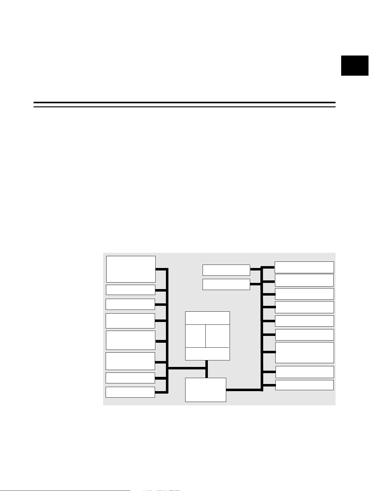
NN
1.1 Introduction
The EP9301 is a highly integrated system-on-chip processor that paves the
way for a multitude of next-generation consumer and industrial electronic
products. Designers of digital media servers and jukeboxes, telematic control
systems, thin clients, set-top boxes, point-of-sale terminals, industrial controls,
biometric security systems, and GPS devices will benefit from the EP9301’s
integrated architecture and advanced features. In fact, with amazingly agile
performance provided by a 166 MHz ARM920T processor, and featuring an
incredibly wide breadth of peripheral interfaces, the EP9301 is well suited to
an even broader range of high volume applications. Furthermore, by enabling
or disabling the EP9301’s peripheral interfaces, designers can reduce
development costs and accelerate time-to-market by creating a single platform
that can be easily modified to deliver a variety of differentiated end products.
Figure 1-1. EP9301 Block Diagram
Chapter 1
1Introduction
1
Vectored
Interrupt
Controllers (2)
Boot ROM
SDRAM
SRAM/
FLASH/ROM
12 Channel DMA
Engine
1/10/100 Ethernet
MAC
JTAG
USB Host, 2 Ports
1.2 EP9301 Features
The EP9301 system-on-chip processor has the following features:
AMBA High-Speed Bus (AHB)
UART1 w/ HDLC
UART2 w/ IrDA
ARM920T
I-Cache
D-Cache
16KB
AHB/APB
16KB
MMU
Bridge
2
S (IIS)
I
System Ctrl - PLLs (2)
Enhanced GPIO
EEPROM, LED (2)
Watchdog Timer
AMBA Peripheral Bus (APB)
RTC with Trim
ADC
SPI
Timers
AC’97
EP9301 User’s Manual - DS636UM2 23
Copyright 2004 Cirrus Logic
Page 24

Introduction
1
• 166 MHz ARM920T Processor
• 16 KByte data cache and 16 KByte instruction cache
• MMU enabling Linux
• 66 MHz system bus
™
• MaverickKey
• 32-bit unique ID
• 128-bit random ID
Integrated Peripheral Interfaces
• 1/10/100 Mbps Ethernet MAC
• Two-port USB 2.0 Full Speed host (OHCI)
• Two UARTs (16550 Type)
• IrDA interface, slow and fast mode
• Analog-to-Digital Converter (ADC)
• Serial Peripheral Interface (SPI) port
• AC ‘97 interface
IDs for Digital Rights Management or Design IP Security
®
and Windows® CE
• I2S interface, up to 2 channels
• External Memory Options
• 16-bit SDRAM interface, up to four banks
• 16/8-bit SRAM/Flash/ROM interface (I/F)
• Serial EEPROM interface
Internal Peripherals
• Real-Time clock with software trim
• 12 DMA channels for data transfer that maximizes system
performance
•Boot ROM
• Dual PLLs control all clock domains
• Watchdog timer
• Two general purpose 16-bit timers
• General purpose 32-bit timer
• 40-bit debug timer
• General-Purpose I/Os
• 16 enhanced GPIOs including interrupt capability
24 EP9301 User’s Manual - DS636UM2
Copyright 2004 Cirrus Logic
Page 25

Introduction
NN
• 31 additional optional GPIOs multiplexed on peripherals
• Available in 208-pin LQFP package
1.3 EP9301 Applications
The EP9301 can be used in a variety of applications, such as:
• Digital media servers
• Integrated home media gateways
• Digital audio jukeboxes
• Portable audio/video players
• Streaming audio/video players
• Telematic control systems
• Set-top boxes
• Point-of-sale terminals
• Thin clients
• Internet TVs
• Biometric security systems
1
• Industrial controls
• GPS & fleet management systems
• Educational toys
• Voting machines
• Medical equipment
1.4 Overview of EP9301 Features
1.4.1 High-Performance ARM920T Processor Core
The EP9301 features an advanced ARM920T processor design with an MMU
that supports Linux®, Windows® CE, and many other embedded operating
systems. The ARM920T’s 32-bit microcontroller architecture, with a five-stage
pipeline, delivers impressive performance at very low power. The included 16
KByte instruction cache and 16 KByte data cache provide zero-cycle latency
to the current program and data, or can be locked to provide guaranteed nolatency access to critical instructions and data. For applications with
instruction memory size restrictions, the ARM920T’s compressed Thumb
instruction set provides a space-efficient design that maximizes external
instruction memory usage.
®
EP9301 User’s Manual - DS636UM2 25
Copyright 2004 Cirrus Logic
Page 26

Introduction
1
1.4.2 MaverickKey™ Unique ID Secures Digital Content and OEM Designs
MaverickKey unique hardware programmed IDs provide an excellent solution
to the growing concern over secure Web content and commerce. With Internet
security playing an important role in the delivery of digital media such as books
or music, traditional software methods are quickly becoming unreliable. The
MaverickKey unique IDs provide OEMs with a method of utilizing specific
hardware IDs for DRM (Digital Rights Management) mechanisms.
MaverickKey uses a specific 32-bit ID and a 128-bit random ID that are
programmed into the EP9301 through the use of laser probing technology.
These IDs can then be used to match secure copyrighted content with the ID
of the target device that the EP9301 is powering, and then deliver the
copyrighted information over a secure connection. In addition, secure
transactions can benefit by matching device IDs to server IDs.
MaverickKey IDs can also be used by OEMs and design houses to protect
against design piracy by presetting ranges for unique IDs. For more
information on securing your design using MaverickKey, please contact your
Cirrus Logic sales representative.
1.4.3 Integrated Two-port USB 2.0 Full Speed Host with Transceivers
The EP9301 integrates two USB 2.0 Full Speed host ports. Fully compliant to
the OHCI USB 2.0 Full Speed specification (12 Mbps), the host ports can be
used to provide connections to a number of external devices including mass
storage devices, external portable devices such as audio players or cameras,
printers, or USB hubs. Naturally, the two-port USB host also supports the USB
2.0 Low Speed standard. This provides the opportunity to create a wide array
of flexible system configurations.
1.4.4 Integrated Ethernet MAC Reduces BOM Costs
The EP9301 integrates a 1/10/100 Mbps Ethernet Media Access Controller
(MAC) on the device. With a simple connection to an MII-based external PHY,
an EP9301-based system has easy, high-performance, cost-effective Internet
capability.
1.4.5 Multiple Booting Mechanisms Increase Flexibility
The processor includes a 16 KByte boot ROM to set up standard
configurations. Optionally, the processor may be booted from FLASH memory,
over the SPI serial interface, or through the UART. This boot flexibility makes it
easy to design user-controlled, field-upgradable systems. See Chapter 3 on
page 59, for additional details.
26 EP9301 User’s Manual - DS636UM2
Copyright 2004 Cirrus Logic
Page 27

Introduction
NN
1.4.6 Abundant General Purpose I/Os Build Flexible Systems
The EP9301 includes both enhanced and standard general-purpose I/O pins
(GPIOs). The 16 different enhanced GPIOs may individually be configured as
inputs, outputs, or interrupt-enabled inputs. There are an additional 31
standard GPIOs that may individually be used as inputs, outputs, or opendrain pins. The standard GPIOs are multiplexed with peripheral function pins,
so the number available depends on the utilization of peripherals. Together,
the enhanced and standard GPIOs facilitate easy system design with external
peripherals not integrated on the EP9301.
1.4.7 General-Purpose Memory Interface (SDRAM, SRAM, ROM and FLASH)
The EP9301 features a unified memory address model in which all memory
devices are accessed over a common address/data bus. Memory accesses
are performed via the high-speed processor bus. The SRAM memory
controller supports 8 and 16-bit devices and accommodates an internal boot
ROM concurrently with a 16-bit SDRAM memory.
1.4.8 12-Bit Analog-to-Digital Converter (ADC) Functionality
The EP9301 includes a 12-bit ADC, which can be used for general ADC
functionality. The interface performs all sampling, averaging, ADC range
checking, and control for a wide variety of applications. To improve system
performance, the converter only interrupts the processor when a meaningful
change occurs.
1
EP9301 User’s Manual - DS636UM2 27
Copyright 2004 Cirrus Logic
Page 28

1
Introduction
This page intentionally blank.
28 EP9301 User’s Manual - DS636UM2
Copyright 2004 Cirrus Logic
Page 29

Chapter 2
OO
2ARM920T Core and Advanced High-Speed Bus (AHB)
2.1 Introduction
This section discusses the ARM920T processor core and the Advanced HighSpeed Bus (AHB).
2.2 Overview: ARM920T Processor Core
The ARM920T is a Harvard architecture processor core with separate
16 kbyte instruction and data caches with an 8-word line length used in the
EP9301. The processor core utilizes a five-stage pipeline consisting of fetch,
decode, execute, data memory access, and write stages.
2.2.1 Features
Key features include:
• ARM V4T (32-bit) and Thumb (16-bit compressed) instruction sets
• 32-bit Advanced Micro-Controller Bus Architecture (AMBA)
2
• 16 kbyte Instruction Cache with lockdown
• 16 kbyte Data Cache (programmable write-through or write-back) with
lockdown
• Write Buffer
• MMU for Microsoft Windows CE and Linux operating systems
• Translation Look-aside Buffers (TLB) with 64 Data and 64 Instruction
Entries
• Programmable Page Sizes of 64 kbyte, 4 kbyte, and 1 kbyte
• Independent lockdown of TLB Entries
• JTAG Interface for Debug Control
EP9301 User’s Manual - DS636UM2 29
Copyright 2004 Cirrus Logic
Page 30
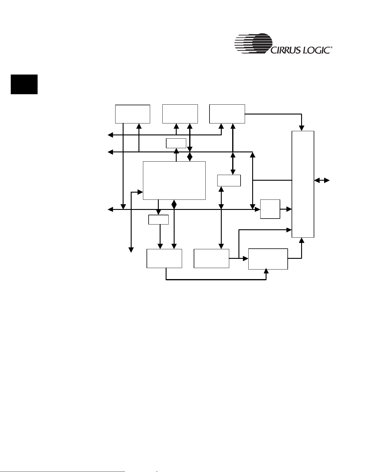
2
ARM920T Core and Advanced High-Speed Bus (AHB)
2.2.2 Block Diagram
Figure 2-1. ARM920T Block Diagram
External
Co-Proc
Interface
JTAG
Instruction
cache
R13
ARM9TDMI
Processor core
(Integral
EmbeddedICE)
R13
Data cache Data MMU
Instruction
MMU
CP15
Write
Buffer
Write Back
PA TAG
RAM
AMBA
Bus
Int.
APB
2.2.3 Operations
The ARM920T core follows a Harvard architecture and consists of an
ARM9TDMI core, MMU, instruction and data cache. The core supports both
the 32-bit ARM and 16-bit Thumb instruction sets.
The internal bus structure (AMBA) includes both an internal high speed and
external low speed bus. The high speed bus AHB (Advanced Highperformance Bus) contains a high speed internal bus clock to synchronize
coprocessor, MMU, cache, DMA controller, and memory modules. AMBA
includes a AHB/APB bridge to the lower speed APB (Advanced Peripheral
Bus). The APB bus connects to lower speed peripheral devices such as
UARTs and GPIOs.
The MMU provides memory address translation for all memory and
peripherals designed to remap memory devices and peripheral address
locations. Sections, large, small and tiny pages are programmable to map
memory in 1 Mbyte, 64 kbyte, 4 kbyte, 1 kbyte size blocks. To increase system
30 EP9301 User’s Manual - DS636UM2
Copyright 2004 Cirrus Logic
Page 31

ARM920T Core and Advanced High-Speed Bus (AHB)
performance, a 64-entry translation look-aside buffer will cache 64 address
locations before a TLB miss occurs.
OO
A 16 kbyte instruction and a 16 kbyte data cache are included to increase
performance for cache-enabled memory regions. The 64-way associative
cache also has lock-down capability. Cached instructions and data also have
access to a 16-word data and 4-word instruction write buffer to allow cached
instructions to be fetched and decoded while the write buffer sends the
information to the external bus.
The ARM920T core supports a number of coprocessors by means of a
specific pipeline architecture interface.
2.2.3.1 ARM9TDMI Core
ARM9TDMI core is responsible for executing both 32-bit ARM and 16-bit
Thumb instructions. Each provides a unique advantage to a system design.
Internally, the instructions enter a 5-stage pipeline. These stages are:
• Instruction Fetch
• Instruction Decode
• Execute
• Data Memory Access
• Register Write
All instructions are fully interlocked. This mechanism will delay the execution
stage of a instruction if data in that instruction comes from a previous
instruction that is not available yet. This simply insures that software will
function identically across different implementations.
2
For memory access instructions, the base register used for the access will be
restored by the processor in the event of an Abort exception. The base
register will be restored to the value contained in the processor register before
execution of the instruction.
The ARM9TDMI core memory interface includes a separate instruction and
data interface to allow concurrent access of instructions and data to reduce
the number of CPI (cycles per instruction). Both interfaces use pipeline
addressing. The core can operate in big and little endian mode. Endianess
affects both the address and the data interfaces.
The memory interface executes four types of memory transfers: sequential,
non-sequential, internal, and coprocessor. It will also support uni- and bidirectional transfer modes.
The core provides a debug interface called JTAG (Joint Testing Action Group).
This interface provides debug capability with five external control signals:
• TDO - Test Data Out
EP9301 User’s Manual - DS636UM2 31
Copyright 2004 Cirrus Logic
Page 32

ARM920T Core and Advanced High-Speed Bus (AHB)
• TDI - Test Data In
• TMS - Test Mode Select
2
• TCK - Test Clock
• nTRST - Test Reset
There are six scan chains (0 through 5) in the ARM9TDMI controlled by the
JTAG Test Access Port (TAP) controller. Details on the individual scan chain
function and bit order can be found in the ARM920T Technical Reference
Manual.
2.2.3.2 Memory Management Unit
The MMU provides the translation and access permissions for the address
and data ports for the ARM9TDMI core. The MMU is controlled by page tables
stored in system memory and accessed using the CP15 register 1. The main
features of the MMU are as follows:
• Address Translation
• Access Permissions and Domains
• MMU Cache and Write Buffer Access
2.2.3.2.1 Address Translation
The virtual address from the ARM920T core is modified by R13 internally to
create a modified virtual address. The MMU then translates the modified
virtual address from R13 by the CP15 register 3 into a physical address to
access external memory or a device. The MMU looks for the physical address
from the Translation Table Base (TTB) in system memory. It will also update
the TLB cache.
The TLB is two 64-entry caches, one for data and one for instruction. If the
physical address for the current virtual address is not found in the TLB (miss),
the processor will go to external memory and look for the TTB in system
memory. The internal translation table walks hardware steps through the page
table setup in external memory for the appropriate physical address.
When the physical address is acquired, the TLB is updated. When the address
is found in the TLB, system performance will increase since it will take
additional cycles to access memory and update the TLB.
Translation of system memory is done by breaking up the memory into
different size blocks called sections, large pages, small pages, and tiny pages.
System memory and registers can be remapped by the MMU. The block sizes
are as follows:
• Section - 1 Mbyte
• Large Page - 64 kbyte
32 EP9301 User’s Manual - DS636UM2
Copyright 2004 Cirrus Logic
Page 33

• Small Page - 16 kbyte
• Tiny Page - 1 kbyte
ARM920T Core and Advanced High-Speed Bus (AHB)
OO
2.2.3.2.2 Access Permission and Domains
Access to any section or page of memory is dependent on its domain. The
page table in external memory also contains access permissions for all subdivisions of external memory. Access to specific instructions or data has three
possible states, assuming access is permitted:
•
Client
: Access permissions based on the section or page table descriptor
•
•
2.2.3.2.3 MMU Enable
Enabling the MMU allows for system memory control, but is also required if
the data cache and the write buffer are to be used. These features are
enabled for specific memory regions, as defined in the system page table.
MMU enable is done via CP15 register 1. The procedure is as follows:
1. Program the Translation Table Base (TTB) and domain access control
2. Create level 1 and level 2 pages for the system and enable the cache and
Manager
descriptor
No access
registers.
the write buffer.
: Ignore access permissions in the section or page table
: any attempted access generates a domain fault
2
3. Enable MMU - bit 0 of CP15 register 1.
2.2.3.3 Cache and Write Buffer
Cache configuration is 64-way set associative. There is a separate 16 kbyte
instruction and data cache. The cache has the following characteristics:
• 8 words per line with 1 valid bit and 2 dirty bits per line for allowing halfline write-backs.
• Write-through and write-back capable, selectable per memory region
defined by the MMU.
• Pseudo random or round robin replacement algorithms for cache misses.
This is determined by the RR bit (bit 14 in CP15 register 1). An 8-word line
is reloaded on a cache miss.
• Independent cache lock-down with granularity of 1/64th of total cache
size or 256 bytes for both instructions and data. Lock-down of the cache
will prevent an eight-word cache line fill of that region of cache.
• For compatibility with Windows CE and to reduce latency, physical
addresses stored for data cache entries are stored in the PA TAG RAM to
EP9301 User’s Manual - DS636UM2 33
Copyright 2004 Cirrus Logic
Page 34

ARM920T Core and Advanced High-Speed Bus (AHB)
be used for cache line write-back operations without need of the MMU,
which prevents a possible TLB miss that would degrade performance.
2
• Write Buffer is a 4-word instruction x 16-word data buffer. If enabled,
writes are sent to buffer directly from cache or from the CPU in the event
of a cache miss or cache not enabled.
2.2.3.3.1 Instruction Cache Enable
• At reset, the cache is disabled.
• A write to CP15 register 1, bit 12, will enable or disable the Instruction
Cache. If the Instruction Cache (I-Cache) is enabled without the MMU
enabled, all accesses are treated as cacheable.
• If disabled, current contents are ignored. If re-enabled before a reset,
contents will be unchanged but may not be coherent with main memory. If
so, contents must be flushed before re-enabling.
2.2.3.3.2 Data Cache Enable
• A write to CP15 register 1, bit 0, will enable or disable the Data Cache (DCache)/Write Buffer.
• D-Cache must only be enabled when the MMU is enabled. All data
accesses are subject to MMU and permission checks.
• If disabled, current contents are ignored. If re-enabled before a reset,
contents will be unchanged but may not be coherent with main memory.
Depending on system software, a clean and invalidate action may be
required before re-enabling.
2.2.3.3.3 Write Buffer Enable
• The Write bugger is enabled by the page table entries in the MMU. The
Write buffer is not enabled unless MMU is enabled.
2.2.4 AMBA AHB Bus Interface Overview
The AMBA AHB is designed for use with high-performance, high clock
frequency system modules. The AHB acts as the high-performance system
backbone bus. AHB supports the efficient connection of processors, on-chip
memories and off-chip external memory interfaces with low-power peripheral
functions. AHB is also specified to ensure ease of use in an efficient design
flow using synthesis and automated test techniques. Figure 2-2 shows a
typical AMBA AHB System.
AHB (Advanced High-Performance Bus) connects with devices that require
greater bandwidth, such as DMA controllers, external system memory, and
coprocessors. The AMBA AHB bus has the following characteristics:
• Burst Transactions
34 EP9301 User’s Manual - DS636UM2
Copyright 2004 Cirrus Logic
Page 35
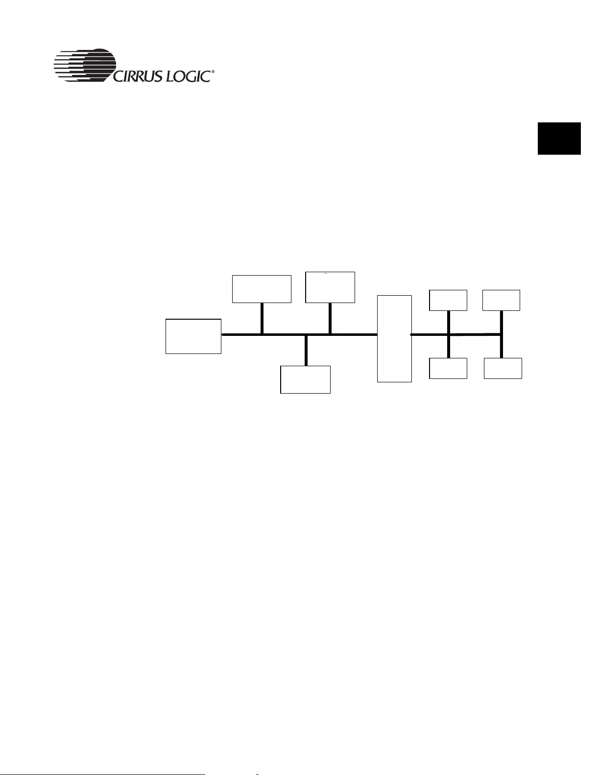
ARM920T Core and Advanced High-Speed Bus (AHB)
• Split Transactions
• Bus Master hand-over to devices, that is, DSP or DMA controller
OO
• Single clock edge operations
APB (Advanced Peripheral Bus) is a lower bandwidth lower power bus which
provides the following:
• Low Power Operations
• Latched address and control
• Simple Interface
Figure 2-2. Typical AMBA AHB System
External
Memory
Inte rfa c e
ARM9TDMI
Co-
Processo
USB
r
AHB APB
DMA
Controller
AHB/
APB
B
r
i
d
g
e
UART SPI
GPIO
AC97
2
EP9301 User’s Manual - DS636UM2 35
Copyright 2004 Cirrus Logic
Page 36
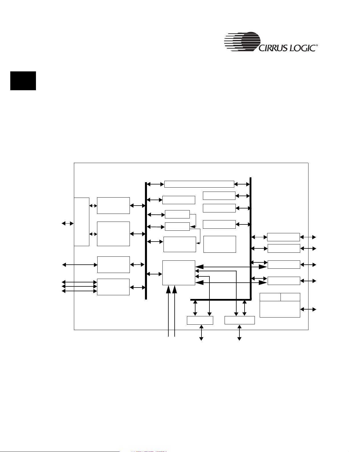
2
ARM920T Core and Advanced High-Speed Bus (AHB)
2.2.5 EP9301 AHB Implementation Details
Peripherals that have high bandwidth or latency requirements are connected
to the EP9301 processor using the AHB bus. These include the external
memory interface, Vectored Interrupt Controllers (VIC1, VIC2), DMA, USB
host, Ethernet MAC and the bridge to the APB interface. The AHB/APB Bridge
transparently converts the AHB access into the slower speed APB accesses.
All of the control registers for the APB peripherals are programmed using the
AHB/APB bridge interface. The main AHB data and address lines are
configured using a multiplexed bus. This removes the need for three state
buffers and bus holders and simplifies bus arbitration. Figure 2-3 shows the
main data paths in the EP9301 AHB implementation.
Figure 2-3. EP9301 Main Data Paths
AHB
AHB/APB Bridge
SDRAM
Controller
E
B
I
Static
Memory
Controller
Ethernet
USB
Host
Boot ROM
VIC2
VIC1
ARM920T
DMA
UARTs
Timers
RTC
Watchdog
Test
Support
APB
GPIOs
SPI
I2S
IrDA
PLL1 PLL2
Clock & State
Control
AC97
Before an AMBA-to-AHB transfer can commence, the bus master must be
granted access to the bus. This process is started by the master asserting a
request signal to the arbiter. Then the arbiter indicates when the master will be
granted use of the bus. A granted bus master starts an AMBA-to-AHB transfer
by driving the address and control signals. These signals provide information
on the address, direction and width of the transfer, as well as indicating
whether the transfer forms part of a burst.
36 EP9301 User’s Manual - DS636UM2
Copyright 2004 Cirrus Logic
Page 37

ARM920T Core and Advanced High-Speed Bus (AHB)
Two different forms of burst transfers are allowed:
• Incrementing bursts, which do not wrap at address boundaries
OO
• Wrapping bursts, which wrap at particular address boundaries.
A write data bus is used to move data from the master to a slave, while a read
data bus is used to move data from a slave to the master. Every transfer
consists of:
• An address and control cycle
• One or more cycles for the data.
In normal operation a master is allowed to complete all the transfers in a
particular burst before the arbiter grants another master access to the bus.
However, in order to avoid excessive arbitration latencies, it is possible for the
arbiter to break up a burst, and, in such cases, the master must re-arbitrate for
the bus in order to complete the remaining transfers in the burst.
2.2.6 Memory and Bus Access Errors
There are several possible sources of access errors.
• Reads to reserved or undefined register memory addresses will return
indeterminate data. Writes to reserved or undefined memory addresses
are generally ignored, but this behavior is not guaranteed. Many register
addresses are not fully decoded, so aliasing may occur. Addresses and
memory ranges listed as Reserved should not be accessed; access
behavior to these regions is not defined.
2
• Access to non-existent registers or memory may result in a bus error.
• Any access in the APB control register space will complete normally, as
these devices have no means of signaling an error.
• Access to non-existent AHB/APB registers may result in a bus error,
depending on the device and nature of the error. Device specific access
rules are defined in the device descriptions.
• External memory access is controlled by the Static Memory Controller
(SMC) and the Synchronous Dynamic RAM (SDRAM) controller. In
general, access to non-existent external memory will complete normally,
with reads returning random false data.
2.2.7 Bus Arbitration
The arbitration mechanism is used to ensure that only one master has access
to the bus it controls at any one time. The arbiter performs this function by
observing a number of different requests to use the bus and deciding which is
currently the highest priority master requesting the bus.
EP9301 User’s Manual - DS636UM2 37
Copyright 2004 Cirrus Logic
Page 38

ARM920T Core and Advanced High-Speed Bus (AHB)
The arbitration scheme can be broken down into three main areas:
• The main AHB system bus arbiter
2
• The SDRAM slave interface arbiter
• The EBI bus arbiter
2.2.7.1 Main AHB Bus Arbiter
This arbiter controls the bus master arbitration for the AHB bus. The AHB bus
has several Master interfaces. These are:
• ARM920T
• DMA controller
• USB host (USB1, 2)
• Ethernet MAC
These interfaces have an order of priority that is linked closely with the power
saving modes. The power saving modes of Halt and Standby force the arbiter
to grant the default bus master, in this case, the ARM920T.
In summary, the order of priority of the bus masters, from highest to lowest, is
shown in Table 2-1.
Table 2-1: AHB Arbiter Priority Scheme
Priority Number
1 MAC MAC DMA DMA
2 USB USB USB MAC
3 DMA ARM920T MAC USB
4 ARM920T DMA ARM920T ARM920T
PRIOR 00
(Reset value)
PRIOR 01 PRIOR 10 PRIOR 11
The priority of the Arbiter can be programmed in the BusMstrArb register in
the Clock and State Controller. The Arbiter can also be programmed to
degrant one of the following masters: DMA, USB Host or Ethernet MAC, if an
interrupt (IRQ or FIQ) is pending or being serviced. This prevents one of these
masters from blocking important interrupt service routines. These masters are
prevented from accessing the bus, and their bus requests are masked, until
the IRQ/FIQ is removed (by the Interrupt Service Routine), at which point their
bus requests will be recognized. The default is to program the Arbiter so that it
not
does
degrant any of these masters.
In normal operation, when the ARM920T is granted the bus and a request to
enter Halt mode is received, the ARM920T is de-granted from the AHB bus.
Any other master requesting the bus in Halt mode (according to the priority)
will be granted the bus. In the case of the entry into Standby, the dummy
master will be granted the bus, which simply performs IDLE transfers. In this
38 EP9301 User’s Manual - DS636UM2
Copyright 2004 Cirrus Logic
Page 39

ARM920T Core and Advanced High-Speed Bus (AHB)
way, all the masters except the ARM920T can be used during Halt mode, but
are shutdown during an entry into Standby.
OO
2.2.7.2 EBI Bus Arbiter
This arbiter is used to arbitrate between accesses from the SDRAM controller
and the Static Memory controller. The priority is given to accesses from the
SDRAM controller.
2.3 AHB Decoder
The AHB decoder contains the memory map for all the AHB masters/slaves
and the APB bridge. When a particular address range is selected, the
appropriate signal is generated. It is defined in Table 2-2.
(For additional information, see “Reference Documents”, on Page 4.)
2
EP9301 User’s Manual - DS636UM2 39
Copyright 2004 Cirrus Logic
Page 40
2
ARM920T Core and Advanced High-Speed Bus (AHB)
Table 2-2: AHB Peripheral Address Range
Address Range Register Width Peripheral Type Peripheral
0x800D_0000 - 0x800F_FFFF - - Reserved
0x800C_0000 - 0x800C_FFFF 32 AHB VIC2
0x800B_0000 - 0x800B_FFFF 32 AHB VIC1
0x800A_0000 - 0x800A_FFFF - - Reserved
0x8009_0000 - 0x8009_FFFF 32 AHB
0x8008_0000 - 0x8008_FFFF 32 AHB SRAM Controller
0x8007_0000 - 0x8007_FFFF - - Reserved
0x8006_0000 - 0x8006_FFFF 32 AHB SDRAM Controller
0x8005_0000 - 0x8005_FFFF - - Reserved
0x8004_0000 - 0x8004_FFFF - - Reserved
0x8003_0000 - 0x8003_FFFF - - Reserved
0x8002_0000 - 0x8002_FFFF 32 AHB USB Host
0x8001_0000 - 0x8001_FFFF 32 AHB Ethernet MAC
0x8000_0000 - 0x8000_FFFF 32 AHB DMA
Note: Due to decoding optimization, the AHB peripheral registers are aliased
throughout each peripherals register bank. Do not program access to an
unspecified register within the bank.
Boot ROM physical
address
2.3.1 AHB Bus Slave
An AHB slave responds to transfers initiated by bus masters within the
system. The slave uses signals from the decoder to determine when it should
respond to a bus transfer. All other signals required for the transfer, such as
the address and control information, are generated by the bus master.
2.3.2 AHB to APB Bridge
The AHB to APB bridge is an AHB slave, providing an interface between the
high-speed AHB and the low-power APB. Read and write transfers on the
AHB are converted into equivalent transfers on the APB. As the APB is not
pipelined. Wait states are added during transfers to and from the APB when
the AHB is required to wait for the APB.
The main sections of this module are:
• AHB slave bus interface
• APB transfer state machine, which is independent of the device memory
map
• APB output signal generation.
40 EP9301 User’s Manual - DS636UM2
Copyright 2004 Cirrus Logic
Page 41

ARM920T Core and Advanced High-Speed Bus (AHB)
2.3.2.1 Function and Operation of APB Bridge
The APB bridge responds to transaction requests from the currently granted
AHB master. The AHB transactions are then converted into APB transactions.
If an undefined location is accessed, operation of the system continues as
normal, but no peripherals are selected. The APB bridge acts as the only
master on the APB.
The APB memory map is shown in Table 2-3.
Table 2-3: APB Peripheral Address Range
OO
2
Address Range
0x8095_0000 - 0x9000_FFFF - - Reserved
0x8094_0000 - 0x8094_FFFF 16 APB Watchdog Timer
0x8093_0000 - 0x8093_FFFF 32 APB Syscon
0x8092_0000 - 0x8092_FFFF 32 APB Real time clock
0x8091_0000 - 0x8091_FFFF - - Reserved
0x8090_0000 - 0x8090_FFFF - - Reserved
0x808F_0000 - 0x808F_FFFF - - Reserved
0x808E_0000 - 0x808E_FFFF - - Reserved
0x808D_0000 - 0x808D_FFFF 8 APB UART2
0x808C_0000 - 0x808C_FFFF 32 APB UART1
0x808B_0000 - 0x808B_FFFF 32 APB IrDA
0x808A_0000 - 0x808A_FFFF 16 APB SPI
0x8089_0000 - 0x8089_FFFF - - Reserved
0x8088_0000 - 0x8088_FFFF 32 APB AAC
0x8087_0000 - 0x8087_FFFF - - Reserved
0x8086_0000 - 0x8086_FFFF - - Reserved
0x8085_0000 - 0x8085_FFFF - - Reserved
0x8084_0000 - 0x8084_FFFF 16 APB GPIO
0x8083_0000 - 0x8083_FFFF 32 APB Security
0x8082_0000 - 0x8082_FFFF 32 APB I2S
0x8081_0000 - 0x8081_FFFF 32 APB Timers
0x8080_0000 - 0x8080_FFFF - - Reserved
0x8010_0000 - 0x807F_FFFF - - Reserved
Register
Width
Peripheral
Type
Peripheral
Note: Due to decoding optimization, the APB peripheral registers are aliased
throughout each peripherals register bank. Do not program access to an
unspecified register within the bank.
2.3.3 APB Bus Slave
An APB slave responds to transfers initiated by bus masters within the
system. The slave uses signals from the decoder to determine when it should
respond to a bus transfer. All other signals required for the transfer, such as
the address and control information, are generated by the APB bridge.
EP9301 User’s Manual - DS636UM2 41
Copyright 2004 Cirrus Logic
Page 42

2
ARM920T Core and Advanced High-Speed Bus (AHB)
2.3.4 Register Definitions
ARM has thirty seven 32-bit internal registers, some are modal, some are
banked. If operating in Thumb mode, the processor must switch to ARM mode
before taking an exception. The return instruction will restore the processor to
Thumb state. Most tasks are executed out of User mode.
User: Unprivileged normal operating mode
FIQ: Fast interrupt (high priority) mode when FIQ is asserted
IRQ: Interrupt request (normal) mode when IRQ is asserted
Supervisor: Software interrupt instruction (SWI) or reset will cause entry
into this mode
Abort: Memory access violation will cause entry into this mode
Undef: Undefined instructions
System: Privileged mode. Uses same registers as user mode
Table 2-4 illustrates the use of all registers for the following ARM920T
operating modes. Each will bank or store a specific number of registers.
Banked register information is not shared between modes. FIQs bank the
fewest number of registers which increases performance.
42 EP9301 User’s Manual - DS636UM2
Copyright 2004 Cirrus Logic
Page 43

Table 2-4: Register Organization Summary
User System Supervisor Abort Undefined IRQ FIQ
r0 r0 r0 r0 r0 r0 r0
r1 r1 r1 r1 r1 r1 r1
r2 r2 r2 r2 r2 r2 r2
r3 r3 r3 r3 r3 r3 r3
r4 r4 r4 r4 r4 r4 r4
r5 r5 r5 r5 r5 r5 r5
r6 r6 r6 r6 r6 r6 r6
r7 r7 r7 r7 r7 r7 r7
r8 r8 r8 r8 r8 r8
r9 r9 r9 r9 r9 r9
r10 r10 r10 r10 r10 r10
r11 r11 r11 r11 r11 r11
r12 r12 r12 r12 r12 r12
r13(sp) r13
r14(lr) r14
r15(pc) pc pc pc pc pc pc
ARM920T Core and Advanced High-Speed Bus (AHB)
Privileged Modes
Exception Modes
r8_fiq
r9_fiq
r10_fiq
r11_fiq
r12_fiq
r13_svc r13_abt r13_und r13_irq r13_fiq
r14_svc r14_abt r14_und r14_irq r14_fiq
OO
2
Thumb
state low
registers
Thumb
state high
registers
cpsr cpsr cpsr cpsr cpsr cpsr cpsr
spsr_svc spsr_abt spsr_und spsr_irq spsr_fiq
Note: Colored areas represent banked registers.
User mode in Thumb state generally limits access to r0-r7. There are six
instructions that allow access to the high registers. For these 6 exceptions, the
processor must revert to ARM state. These exceptions are:
• r0-r12: General purpose read/write 32-bit registers
• r13 (sp): Stack Pointer
• r14 (lr): Link Register
• r15 (pc): Program Counter
• cpsr: Current Program Status Register (contains condition codes and
operating modes)
• spsr: Saved Program Status Register (saves CPSR when exception
EP9301 User’s Manual - DS636UM2 43
Copyright 2004 Cirrus Logic
Page 44

2
ARM920T Core and Advanced High-Speed Bus (AHB)
occurs)
The ARM920T core has 16 coprocessor registers for control over the core.
Updates to the coprocessor registers are written using the CP15 instruction.
Table 2-5 describes the CP15 ARM920T registers.
Table 2-5: CP15 ARM920T Register Description
Register Description
ID Code: (Read/Only) This register returns a 32-bit device code. ID Code data represents
the core type, revision, part number etc. Access to this register is done with the following
instruction:
0
1
MRC p15 0, Rd, c0, c0, 0
Cache Code: This will also return cache type, size and length of both I-Cache and D-
Cache, size, and associativity. This is accessed with:
MRC p15 0, Rd, c0, c0, 1
Control Register: (Read/Write) Use this register to enable MMU, instruction and data
cache, round robin replacement ‘RR’-bit, system protection, ROM protection, clocking
mode. Read/Write Instructions:
MRC p15, 0, Rd, c1, c0, 0 - Read control register - value stored in Rd
MCR p15, 0, Rd, c1, c0, 0 - Write control register - value first loaded into Rd
Translation Base Table: (Read/Write) This register contains the start address of the first
level translation table. Upper18 bits represent the pointer to table base. Lower 14 bits
2
3
4
5
6
7
8
should be 0 for a write, unpr edictable if read.
MRC p15, 0, Rd, c2, c0, 0 - Read TTB
MCR p15, 0, Rd, c2, c0, 0 - Write TTB
Domain Access Control: (Read/Write) This register specifies permissions for all 16
domains.
MRC p15, 0, Rd, c3, c0, 0
MCR p15, 0, Rd, c3, c0, 0
Reserved: Do not access. Unpredictable behavior may result.
Fault Status: (Read/Write) This register indicates type of fault and domain of last data
abort.
MRC p15, 0, Rd, c5, c0, 0 - read data FSR value
MCR p15, 0, Rd, c5, c0, 0 - write data FSR value
Fault Address: (Read/Write) This register contains address of the last data access abort.
MRC p15, 0, Rd, c6, c0, 0 - read data FAR data
MCR p15, 0, Rd, c6, c0, 0 - write data FAR data
Cache Operation: (Write/Only) This register will configure or perform a clean (flush) of the
cache and write buffer when written to. An example:
MRC p15, 0, Rd, c7, c7, 0 - Invalidate I/D-cache
MRC p15, 0, Rd, c7, c5, 0 - Invalidate I-Cache
TLB Operation: (Write/Only) This register can configure or clean (flush) when written to:
MRC p15, 0, Rd, c8, c7, 0 - Invalidate TLB
Cache Lockdown: (Read/Write) Prevents certain cache-line fills from being overwritten
9
(locked).
MRC p15, 0, Rd, c9, c0, 1- Write lockdown base pointer for D -Cache
MRC p15, 0, Rd, c9, c0, 1 - Write lockdown base pointer for I-Cache
44 EP9301 User’s Manual - DS636UM2
Copyright 2004 Cirrus Logic
Page 45

Table 2-5: CP15 ARM920T Register Description (Continued)
Register Description
ARM920T Core and Advanced High-Speed Bus (AHB)
OO
11,12,14
2.3.5 Memory Map
The overall memory map for the device is shown in Table 2-6.
If internal Boot Mode is selected and the register BootModeClr has been
written, the address range 0x0000_0000 -> 0x0000_FFFF is occupied by the
internal Boot ROM until the internal Boot Code is completed and then the map
reverts back to either Synchronous or Asynchronous memory in this address
space.
NOTE: Some memory locations are listed as Reserved. These memory
locations should not be used. Reading from these memory locations will yield
invalid data. Writing to these memory locations may cause unpredictable
results.
10
13
15
TLB Lockdown: (Read/Write) Prevents TLB entries from being erased during a table walk.
MRC p15, 0, Rd, c10, c0, 1- Write lockdown base pointer for data TLB entry
MRC p15, 0, Rd, c10, c0, 1 - Write lockdown base pointer for instruction TLB entry
Reserved
FCSE PID Register: (Read/Write) Addresses by the ARM9TDMI core in a range from 0 to
32 MB are translated by this register to A + FCSE*32MB and remapped. If turned off,
straight address map to the MMU results.
Test Register Only: Reads or writes will cause unpredictable behavior.
2
Table 2-6: Global Memory Map for the Two Boot Modes
Address Range Sync Memory Boot Async Memory Boot
ASD0 Pin = 1 ASD0 Pin = 0
0xF000_0000 - 0xFFFF_FFFF Async memory (nCS0) Sync memory (nSDCE3)
0xE000_0000 - 0xEFFF_FFFF Sync memory (nSDCE2) Sync memory (nSDCE2)
0xD000_0000 - 0xDFFF_FFFF Sync memory (nSDCE1) Sync memory (nSDCE1)
0xC000_0000 - 0xCFFF_FFFF Sync memory (nSDCE0) Sync memory (nSDCE0)
0x9000_0000 - 0xBFFF_FFFF Not Used Not Used
0x8080_0000 - 0x8FFF_FFFF APB mapped registers APB mapped registers
0x8010_0000 - 0x807F_FFFF Reserved Reserved
0x8000_0000 - 0x800F_FFFF AHB mapped registers AHB mapped registers
0x7000_0000 - 0x7FFF_FFFF Async memory (nCS7) Async memory (nCS7)
0x6000_0000 - 0x6FFF_FFFF Async memory (nCS6) Async memory (nCS6)
0x5000_0000 - 0x5FFF_FFFF Reserved Reserved
0x4000_0000 - 0x4FFF_FFFF Reserved Reserved
0x3000_0000 - 0x3FFF_FFFF Async memory (nCS3) Async memory (nCS3)
0x2000_0000 - 0x2FFF_FFFF Async memory (nCS2) Async memory (nCS2)
0x1000_0000 - 0x1FFF_FFFF Async memory (nCS1) Async memory (nCS1)
0x0001_0000 - 0x0FF F_FFFF S ync memory (nSDCE3) Async memory (nCS0)
EP9301 User’s Manual - DS636UM2 45
Copyright 2004 Cirrus Logic
Page 46

ARM920T Core and Advanced High-Speed Bus (AHB)
Table 2-6: Global Memory Map for the Two Boot Modes (Continued)
Address Range Sync Memory Boot Async Memory Boot
2
0x0000_0000 - 0x0000_FFFF
Note: The shaded areas are the memory areas dedicated to system registers. Details
of these registers are in Table 2-7.
2.3.6 Internal Register Map
Registers are set to their default state by the RSTOn pin and by the PRSTn pin
inputs. Some state conserving registers are reset only by the PRSTn pin. All
registers are read/write unless specified otherwise.
2.3.6.1 Memory Access Rules
Any memory address not specifically assigned to a register should be
avoided. Reads to register memory addresses labelled Reserved, Unused or
Undefined will return indeterminate data. Writes to register memory addresses
labelled Reserved, Unused or Undefined are generally ignored, but this
behavior is not guaranteed. Many register addresses are not fully decoded, so
aliasing may occur. Addresses and memory ranges listed as Reserved
(RSVD) should not be accessed; access behavior to these regions is not
defined.
ASD0 Pin = 1 ASD0 Pin = 0
Sync memory (nSDCE3)
or
Internal Boot ROM
if INTBOOT selected
Async memory (nCS0)
Internal Boot ROM
if INTBOOT selected
or
The SW Lock field identifies registers with a software lock. The software lock
prevents the register from being written unless a proper unlock operation is
performed immediately prior to writing the target register. Any register whose
accidental alteration could cause system damage is controlled with a software
lock. Each peripheral with software lock capability has its own software lock
register.
Within a register definition, a reserved bit, indicated the name RSVD, means
the bit is not accessible. Software should mask the RSVD bits when doing bit
reads. RSVD bits will ignore writes, that is writing a zero or a one does not
matter.
Register bits identified as NC must be treated in a specific manner for reads
and writes; see the register description for each register for information on
how to read and write register bits identified as NC. Register bits identified as
NC are functionally alive but have an undocumented or a “don’t care”
operating function. The register description will provide information on how to
handle NC bits.
Unless specified otherwise, all registers can be accessed as a byte, half-word,
or word.
46 EP9301 User’s Manual - DS636UM2
Copyright 2004 Cirrus Logic
Page 47

CAUTION: Some memory locations are listed as Reserved. These memory
locations should not be used. Reading from these memory locations will yield
invalid data. Writing to these memory locations may cause unpredictable
results.
Table 2-7: Internal Register Map
ARM920T Core and Advanced High-Speed Bus (AHB)
OO
2
Address Register Name Register Description
0x8000_xxxx DMA DMA Control Registers
0x8000_0000 - 0x8000_003C M2P Channel 0 Registers (Tx) Memory-to-Peripheral Channel 0 Registers (Tx) N
0x8000_0040 - 0x8000_007C M2P Channel 1 Registers (Rx) Memory-to-Peripheral Channel 1 Registers (Rx) N
0x8000_0080 - 0x8000_00BC M2P Channel 2 Registers (Tx) Memory-to-Peripheral Channel 2 Registers (Tx) N
0x8000_00C0 - 0x8000_00FC M2P Channel 3 Registers (Rx) Memory-to-Peripheral Channel 3 Registers (Rx) N
0x8000_0100 - 0x8000_013C M2M Channel 0 Registers Memory-to-Memory Channel 0 Registers N
0x8000_0140 - 0x8000_017C M2M Channel 1 Registers Memory-to-Memory Channel 1 Registers N
0x8000_0180 - 0x8000_01FC Reserved
0x8000_0200 - 0x8000_023C M2P Channel 5 Registers (Rx) Memory-to-Peripheral Channel 5 Registers (Rx) N
0x8000_0240 - 0x8000_027C M2P Channel 4 Registers (Tx) Memory-to-Peripheral Channel 4 Registers (Tx) N
0x8000_0280 - 0x8000_02BC M2P Channel 7 Registers (Rx) Memory-to-Peripheral Channel 7 Registers (Rx) N
0x8000_02C0 - 0x8000_02FC M2P Channel 6 Registers (Tx) Memory-to-Peripheral Channel 6 Registers (Tx) N
0x8000_0300 - 0x8000_033C M2P Channel 9 Registers (Rx) Memory-to-Peripheral Channel 9 Registers (Rx) N
0x8000_0340 - 0x8000_037C M2P Channel 8 Registers (Tx) Memory-to-Peripheral Channel 8 Registers (Tx) N
0x8000_0380 DMAChArb DMA Channel Arbitration Register N
0x8000_03C0 DMAGlInt DMA Global Interrupt Register N
0x8000_03C4 - 0x8000_FFFC Reserved
0x8001_xxxx
0x8001_0000 RXCtl MAC Receiver Control Register N
0x8001_0004 TXCtl MAC Transmitter Control Register N
0x8001_0008 TestCtl MAC Test Control Register N
0x8001_0010 MIICmd MAC MII Command Register N
0x8001_0014 MIIData MAC MII Data Register N
0x8001_0018 MIISts MAC MII Status Register N
0x8001_0020 SelfCtl MAC Self Control Register N
0x8001_0024 IntEn MAC Interrupt Enable Register N
0x8001_0028 IntStsP MAC Interrupt Status Preserve Register N
0x8001_002C IntStsC MAC Interrupt Status Clear Register N
0x8001_0030 - 0x8001_0034 Reserved
0x8001_0038 DiagAd MAC Diagnostic Address Register N
0x8001_003C DiagDa MAC Diagnostic Data Register N
0x8001_0040 GT MAC General Timer Register N
0x8001_0044 FCT MAC Flow Control Timer Register N
0x8001_0048 FCF MAC Flow Control Format Register N
0x8001_004C AFP MAC Address Filter Pointer Register N
0x8001_0050 - 0x8001_0055 IndAd
Ethernet MAC Ethernet MAC Control Registers
MAC Individual Address Register, (shares address space with
HashTbl)
SW
Lock
N
EP9301 User’s Manual - DS636UM2 47
Copyright 2004 Cirrus Logic
Page 48

ARM920T Core and Advanced High-Speed Bus (AHB)
Table 2-7: Internal Register Map (Continued)
2
Address Register Name Register Description
0x8001_0050 - 0x8001_0057 HashTbl MAC Hash Table Register, (shares address space with IndAd) N
0x8001_0060 GlIntSts MAC Global Interrupt Status Register N
0x8001_0064 GlIntMsk MAC Global Interrupt Mask Register N
0x8001_0068 GlIntROSts MAC Global Interrupt Read Only Status Register N
0x8001_006C GlIntFrc MAC Global Interrupt Force Register N
0x8001_0070 TXCollCnt MAC Transmit Collision Count Register N
0x8001_0074 RXMissCnt MAC Receive Miss Count Register N
0x8001_0078 RXRuntCnt MAC Receive Runt Count Register N
0x8001_0080 BMCtl MAC Bus Master Control Register N
0x8001_0084 BMSts MAC Bus Master Status Register N
0x8001_0088 RXBCA MAC Receive Buffer Current Address Register N
0x8001_0090 RXDQBAdd MAC Receive Descriptor Queue Base Address Register N
0x8001_0094 RXDQBLen MAC Receive Descriptor Queue Base Length Register N
0x8001_0096 RXDQCurLen MAC Receive Descriptor Queue Current Length Register N
0x8001_0098 RXDCurAdd MAC Receive Descriptor Current Address Register N
0x8001_009C RXDEnq MAC Receive Descriptor Enqueue Register N
0x8001_00A0 RXStsQBAdd MAC Receive Status Queue Base Address Register N
0x8001_00A4 RXStsQBLen MAC Receive Status Queue Base Length Register N
0x8001_00A6 RXStsQCurLen MAC Receive Status Queue Current Length Register N
0x8001_00A8 RXStsQCurAdd MAC Receive Status Queue Current Address Register N
0x8001_00AC RXStsEnq MAC Receive Status Enqueue Register N
0x8001_00B0 TXDQBAdd MAC Transmit Descriptor Queue Base Address Register N
0x8001_00B4 TXDQBLen MAC Transmit Descriptor Queue Base Length Register N
0x8001_00B6 TXDQCurLen MAC Transmit Descriptor Queue Current Length Register N
0x8001_00B8 TXDQCurAdd MAC Transmit Descriptor Current Address Register N
0x8001_00BC TXDEnq MAC Transmit Descriptor Enqueue Register N
0x8001_00C0 TXStsQBAdd MAC Transmit Status Queue Base Address Register N
0x8001_00C4 TXStsQBLen MAC Transmit Status Queue Base Length Register N
0x8001_00C6 TXStsQCurLen MAC Transmit Status Queue Current Length Register N
0x8001_00C8 TXStsQCurAdd MAC Transmit Status Queue Current Address Register N
0x8001_00D0 RXBufThrshld MAC Receive Buffer Threshold Register N
0x8001_00D4 TXBufThrshld MAC Transmit Buffer Threshold Register N
0x8001_00D8 RXStsThrshld MAC Receive Status Threshold Register N
0x8001_00DC TXStsThrshld MAC Transmit Status Threshold Register N
0x8001_00E0 RXDThrshld MAC Receive Descriptor Threshold Register N
0x8001_00E4 TXDThrshld MAC Transmit Descriptor Threshold Register N
0x8001_00E8 MaxFrmLen MAC Maximum Frame Length Register N
0x8001_00EC RXHdrLen MAC Receive Header Length Register N
0x8001_0100 - 0x8001_010C Reserved
0x8001_4000 - 0x8001_50FF MACFIFO MAC FIFO RAM N
SW
Lock
0x8002_xxxx
0x8002_0000 HcRevision USB Host Controller Revision N
USB USB Registers
N
48 EP9301 User’s Manual - DS636UM2
Copyright 2004 Cirrus Logic
Page 49

Table 2-7: Internal Register Map (Continued)
ARM920T Core and Advanced High-Speed Bus (AHB)
OO
Address Register Name Register Description
0x8002_0004 HcControl USB Host Controller Control N
0x8002_0008 HcCommandStatus USB Host Controller Command Status N
0x8002_000C HcInterruptStatus USB Host Controller Interrupt Status N
0x8002_0010 HcInterruptEnable USB Host Controller Interrupt Enable N
0x8002_0014 HcInterruptDisable USB Host Controller Interrupt Disable N
0x8002_0018 HcHCCA USB Host Controller HCCA N
0x8002_001C HcPeriodCurrentED USB Host Controller Period CurrentED N
0x8002_0020 HcControlHeadED USB Host Controller Control HeadED N
0x8002_0024 HcControlCurrentED USB Host Controller Control CurrentED N
0x8002_0028 HcBulkHeadED USB Host Controller Bulk HeadED N
0x8002_002C HcBulkCurrentED USB Host Controller Bulk CurrentED N
0x8002_0030 HcDoneHead USB Host Controller Done Head N
0x8002_0034 HcFmInterval USB Host Controller Fm Interval N
0x8002_0038 HcFmRemaining USB Host Controller Fm Remaining N
0x8002_003C HcFmNumber USB Host Controller Fm Number N
0x8002_0040 HcPeriodicStart USB Host Controller Periodic Start N
0x8002_0044 HcLSThreshold USB Host Controller LS Threshold N
0x8002_0048 HcRhDescriptorA USB Host Controller Root Hub Descriptor A N
0x8002_004C HcRhDescriptorB USB Host Controller Root Hub Descriptor B N
0x8002_0050 HcRhStatus USB Host Controller Root Hub Status N
0x8002_0054 HcRhPortStatus[1] USB Host Controller Root Hub Port Status 1 N
0x8002_0058 HcRhPortStatus[2] USB Host Controller Root Hub Port Status 2 N
0x8002_005C HcRhPortStatus[3] USB Host Controller Root Hub Port Status 3 N
0x8002_0080 USBCtrl USB Configuration Control N
0x8002_0084 USBHCI USB Host Controller Interface Status N
SW
Lock
2
0x8006_xxxx
0x8006_0000 Reserved
0x8006_0004 GlConfig Control and status bits used in configuration N
0x8006_0008 RefrshTimr Set the period between refresh cycles N
0x8006_000C BootSts Reflect the state of the boot mode option pins N
0x8006_0010 SDRAMDevCfg0 Device configuration 0 N
0x8006_0014 SDRAMDevCfg1 Device configuration 1 N
0x8006_0018 SDRAMDevCfg2 Device configuration 2 N
0x8006_001C SDRAMDevCfg3 Device configuration 3 N
0x8008_xxxx
0x8008_0000 SMCBCR0
0x8008_0004 SMCBCR1
0x8008_0008 SMCBCR2
EP9301 User’s Manual - DS636UM2 49
Copyright 2004 Cirrus Logic
SDRAM SDRAM Registers
SMC SMC Control Registers
Bank config Register 0 (used to program characteristics of the
SRAM/ROM memory)
Bank config Register 1 (used to program characteristics of the
SRAM/ROM memory)
Bank config Register 2 (used to program characteristics of the
SRAM/ROM memory)
N
N
N
N
Page 50

ARM920T Core and Advanced High-Speed Bus (AHB)
Table 2-7: Internal Register Map (Continued)
2
Address Register Name Register Description
0x8008_000C SMCBCR3
0x8008_0010 - 0x8008_0014 Reserved
0x8008_0018 SMCBCR6
0x8008_001C SMCBCR7
0x8008_0020 - 0x8008_FFFC Reserved
0x8009_xxxx
0x8009_0000 Boot ROM Start N
0x8009_3FFF Boot ROM End N
0x800B_xxxx
0x800B_0000 VIC1IRQStatus IRQ status Register N
0x800B_0004 VIC1FIQStatus FIQ status Register N
0x800B_0008 VIC1RawIntr Raw interrupt status Register N
0x800B_000C VIC1IntSelect Interrupt select Register N
0x800B_0010 VIC1IntEnable Interrupt enable Register N
0x800B_0014 VIC1IntEnClear Interrupt enable clear Register N
0x800B_0018 VIC1SoftInt Software interrupt Register N
0x800B_001C VIC1SoftIntClear Software interrupt clear Register N
0x800B_0020 VIC1Protection Protection enable Register N
0x800B_0030 VIC1VectAddr Vector address Register N
0x800B_0034 VIC1DefVectAddr Default vector address Register N
0x800B_0100 VIC1VectAddr0 Vector address 0 Register N
0x800B_0104 VIC1VectAddr1 Vector address 1 Register N
0x800B_0108 VIC1VectAddr2 Vector address 2 Register N
0x800B_010C VIC1VectAddr3 Vector address 3 Register N
0x800B_0110 VIC1VectAddr4 Vector address 4 Register N
0x800B_0114 VIC1VectAddr5 Vector address 5 Register N
0x800B_0118 VIC1VectAddr6 Vector address 6 Register N
0x800B_011C VIC1VectAddr7 Vector address 7 Register N
0x800B_0120 VIC1VectAddr8 Vector address 8 Register N
0x800B_0124 VIC1VectAddr9 Vector address 9 Register N
0x800B_0128 VIC1VectAddr10 Vector address 10 Register N
0x800B_012C VIC1VectAddr11 Vector address 11 Register N
0x800B_0130 VIC1VectAddr12 Vector address 12 Register N
0x800B_0134 VIC1VectAddr13 Vector address 13 Register N
0x800B_0138 VIC1VectAddr14 Vector address 14 Register N
0x800B_013C VIC1VectAddr15 Vector address 15 Register N
0x800B_0200 VIC1VectCntl0 Vector control 0 Register N
0x800B_0204 VIC1VectCntl1 Vector control 1 Register N
Boot ROM Boot ROM Memory Locations
VIC1 Vectored Interrupt Controller 1 Registers
Bank config Register 3 (used to program characteristics of the
SRAM/ROM memory)
Bank config Register 6 (used to program characteristics of the
SRAM/ROM memory)
Bank config Register 7 (used to program characteristics of the
SRAM/ROM memory)
SW
Lock
N
N
N
50 EP9301 User’s Manual - DS636UM2
Copyright 2004 Cirrus Logic
Page 51
Table 2-7: Internal Register Map (Continued)
ARM920T Core and Advanced High-Speed Bus (AHB)
OO
Address Register Name Register Description
0x800B_0208 VIC1VectCntl2 Vector control 2 Register N
0x800B_020C VIC1VectCntl3 Vector control3 Register N
0x800B_0210 VIC1VectCntl4 Vector control 4 Register N
0x800B_0214 VIC1VectCntl5 Vector control 5 Register N
0x800B_0218 VIC1VectCntl6 Vector control 6 Register N
0x800B_021C VIC1VectCntl7 Vector control 7 Register N
0x800B_0220 VIC1VectCntl8 Vector control 8 Register N
0x800B_0224 VIC1VectCntl9 Vector control 9 Register N
0x800B_0228 VIC1VectCntl10 Vector control 10 Register N
0x800B_022C VIC1VectCntl11 Vector control 11 Register N
0x800B_0230 VIC1VectCntl12 Vector control 12 Register N
0x800B_0234 VIC1VectCntl13 Vector control 13 Register N
0x800B_0238 VIC1VectCntl14 Vector control 14 Register N
0x800B_023C VIC1VectCntl15 Vector control 15 Register N
0x800B_0FE0 VIC1PeriphID0 Peripheral identification Register bits 7:0 N
0x800B_0FE4 VIC1PeriphID1 Peripheral identification Register bits 15:8 N
0x800B_0FE8 VIC1PeriphID2 Peripheral identification Register bits 23:16 N
0x800B_0FEC VIC1PeriphID3 Peripheral identification Register bits 31:24 N
0x800B_0FF0 - 0x800B_0FFC Reserved N
0x800C_xxxx
0x800C_0000 VIC2IRQStatus IRQ status Register N
0x800C_0004 VIC2FIQStatus FIQ status Register N
0x800C_0008 VIC2RawIntr Raw interrupt status Register N
0x800C_000C VIC2IntSelect Interrupt select Register N
0x800C_0010 VIC2IntEnable Interrupt enable Register N
0x800C_0014 VIC2IntEnClear Interrupt enable clear Register N
0x800C_0018 VIC2SoftInt Software interrupt Register N
0x800C_001C VIC2SoftIntClear Software interrupt clear Register N
0x800C_0020 VIC2Protection Protection enable Register N
0x800C_0030 VIC2VectAddr Vector address Register N
0x800C_0034 VIC2DefVectAddr Default vector address Register N
0x800C_0100 VIC2VectAddr0 Vector address 0 Register N
0x800C_0104 VIC2VectAddr1 Vector address 1 Register N
0x800C_0108 VIC2VectAddr2 Vector address 2 Register N
0x800C_010C VIC2VectAddr3 Vector address 3 Register N
0x800C_0110 VIC2VectAddr4 Vector address 4 Register N
0x800C_0114 VIC2VectAddr5 Vector address 5 Register N
0x800C_0118 VIC2VectAddr6 Vector address 6 Register N
0x800C_011C VIC2VectAddr7 Vector address 7 Register N
0x800C_0120 VIC2VectAddr8 Vector address 8 Register N
0x800C_0124 VIC2VectAddr9 Vector address 9 Register N
0x800C_0128 VIC2VectAddr10 Vector address 10 Register N
VIC2 Vectored Interrupt Controller 2 Registers
SW
Lock
2
EP9301 User’s Manual - DS636UM2 51
Copyright 2004 Cirrus Logic
Page 52

ARM920T Core and Advanced High-Speed Bus (AHB)
Table 2-7: Internal Register Map (Continued)
2
Address Register Name Register Description
0x800C_012C VIC2VectAddr11 Vector address 11 Register N
0x800C_0130 VIC2VectAddr12 Vector address 12 Register N
0x800C_0134 VIC2VectAddr13 Vector address 13 Register N
0x800C_0138 VIC2VectAddr14 Vector address 14 Register N
0x800C_013C VIC2VectAddr15 Vector address 15 Register N
0x800C_0200 VIC2VectCntl0 Vector control 0 Register N
0x800C_0204 VIC2VectCntl1 Vector control 1 Register N
0x800C_0208 VIC2VectCntl2 Vector control 2 Register N
0x800C_020C VIC2VectCntl3 Vector control3 Register N
0x800C_0210 VIC2VectCntl4 Vector control 4 Register N
0x800C_0214 VIC2VectCntl5 Vector control 5 Register N
0x800C_0218 VIC2VectCntl6 Vector control 6 Register N
0x800C_021C VIC2VectCntl7 Vector control 7 Register N
0x800C_0220 VIC2VectCntl8 Vector control 8 Register N
0x800C_0224 VIC2VectCntl9 Vector control 9 Register N
0x800C_0228 VIC2VectCntl10 Vector control 10 Register N
0x800C_022C VIC2VectCntl11 Vector control 11 Register N
0x800C_0230 VIC2VectCntl12 Vector control 12 Register N
0x800C_0234 VIC2VectCntl13 Vector control 13 Register N
0x800C_0238 VIC2VectCntl14 Vector control 14 Register N
0x800C_023C VIC2VectCntl15 Vector control 15 Register N
0x800C_0FE0 VIC2PeriphID0 Peripheral identification Register bits 7:0 N
0x800C_0FE4 VIC2PeriphID1 Peripheral identification Register bits 15:8 N
0x800C_0FE8 VIC2PeriphID2 Peripheral identification Register bits 23:16 N
0x800C_0FEC VIC2PeriphID3 Peripheral identification Register bits 31:24 N
0x800C_0FF0 - 0x800C_0FFC Reserved N
SW
Lock
0x8081_xxxx
0x8081_0000 Timer1Load Contains the initial value of the timer N
0x8081_0004 Timer1Value Gives the current value of the timer N
0x8081_0008 Timer1Control Provides enable/disable and mode configurations for the timer N
0x8081_000C Timer1Clear Clears an interrupt generated by the timer N
0x8081_0020 Timer2Load Contains the initial value of the timer N
0x8081_0024 Timer2Value Gives the current value of the timer N
0x8081_0028 Timer2Control Provides enable/disable and mode configurations for the timer N
0x8081_002C Timer2Clear Clears an interrupt generated by the timer N
0x8081_0060 - 0x8081_0064 Reserved
0x8081_0080 Timer3Load Contains the initial value of the timer N
0x8081_0084 Timer3Value Gives the current value of the timer N
0x8081_0088 Timer3Control Provides enable/disable and mode configurations for the timer N
0x8081_008C Timer3Clear Clears an interrupt generated by the timer N
TIMER Timer Registers
52 EP9301 User’s Manual - DS636UM2
Copyright 2004 Cirrus Logic
Page 53
Table 2-7: Internal Register Map (Continued)
ARM920T Core and Advanced High-Speed Bus (AHB)
OO
Address Register Name Register Description
0x8082_xxxx
0x8082_0000 I2STXClkCfg Transmitter clock configuration Register N
0x8082_0004 I2SRXClkCfg Receiver clock configuration Register N
0x8082_0008 I2SGlSts
0x8082_000C I2SGlCtrl I2S Global Control Register N
0x8082_0010 I2STX0Lft Left Transmit data Register for channel 0 N
0x8082_0014 I2STX0Rt Right Transmit data Register for channel 0 N
0x8082_0018 I2STX1Lft Left Transmit data Register for channel 1 N
0x8082_001C I2STX1Rt Right Transmit data Register for channel 1 N
0x8082_0020 I2STX2Lft Left Transmit data Register for channel 2 N
0x8082_0024 I2STX2Rt Right Transmit data Register for channel 2 N
0x8082_0028 I2STXLinCtrlData Transmit Line Control Register N
0x8082_002C I2STXCtrl Transmit Control Register N
0x8082_0030 I2STXWrdLen Transmit Word Length N
0x8082_0034 I2STX0En TX0 Channel Enable N
0x8082_0038 I2STX1En TX1 Channel Enable N
0x8082_003C I2STX2En TX2 Channel Enable N
0x8082_0040 I2SRX0Lft Left Receive data Register for channel 0 N
0x8082_0044 I2SRX0Rt Right Receive data Register for channel 0 N
0x8082_0048 I2SRX1Lft Left Receive data Register for channel 1 N
0x8082_004C I2SRX1Rt Right Receive data Register for channel 1 N
0x8082_0050 I2SRX2Lft Left Receive data Register for channel 2 N
0x8082_0054 I2SRX2Rt Right Receive data Register for channel 2 N
0x8082_0058 I2SRXLinCtrlData Receive Line Control Register N
0x8082_005C I2SRXCtrl Receive Control Register N
0x8082_0060 I2SRXWrdLen Receive Word Length N
0x8082_0064 I2SRX0En RX0 Channel Enable N
0x8082_0068 I2SRX1En RX1 Channel Enable N
0x8082_006C I2SRX2En RX2 Channel Enable N
I2S I2S Registers
I2S Global Status Register. This reflects the status of the 3 RX
FIFOs and the 3 TX FIFOs
SW
Lock
N
2
N
0x8083_xxxx
0x8083_2714 ExtensionID Contains the Part ID for EP93XX devices N
Contact Cirrus Logic for details regarding implementation of device Security measures.
0x8084_xxxx
0x8084_0000 PADR GPIO Port A Data Register N
0x8084_0004 PBDR GPIO Port B Data Register N
0x8084_0008 PCDR GPIO Port C Data Register N
0x8084_000C PDDR GPIO Port D Data Register N
0x8084_0010 PADDR GPIO Port A Data Direction Register N
0x8084_0014 PBDDR GPIO Port B Data Direction Register N
EP9301 User’s Manual - DS636UM2 53
Copyright 2004 Cirrus Logic
SECURITY Security Registers
GPIO GPIO Control Registers
Page 54

ARM920T Core and Advanced High-Speed Bus (AHB)
Table 2-7: Internal Register Map (Continued)
2
Address Register Name Register Description
0x8084_0018 PCDDR GPIO Port C Data Direction Register N
0x8084_001C PDDDR GPIO Port D Data Direction Register N
0x8084_0020 PEDR GPIO Port E Data Register N
0x8084_0024 PEDDR GPIO Port E Data Direction Register N
0x8084_0028 - 0x8084_002C Reserved
0x8084_0030 PFDR GPIO Port F Data Register N
0x8084_0034 PFDDR GPIO Port F Data Direction Register N
0x8084_0038 PGDR GPIO Port G Data Register N
0x8084_003C PGDDR GPIO Port G Data Direction Register N
0x8084_0040 PHDR GPIO Port H Data Register N
0x8084_0044 PHDDR GPIO Port H Data Direction Register N
0x8084_0048 Reserved
0x8084_004C GPIOFIntType1
0x8084_0050 GPIOFIntType2
0x8084_0054 GPIOFEOI GPIO Port F End Of Interrupt Register N
0x8084_0058 GPIOFIntEn Interrupt Enable for Port F N
0x8084_005C IntStsF
0x8084_0060 RawIntStsF
0x8084_0064 GPIOFDB GPIO F Debounce Register N
0x8084_0068 - 0x8084_008C Reserved
0x8084_0090 GPIOAIntType1
0x8084_0094 GPIOAIntType2
0x8084_0098 GPIOAEOI GPIO Port A End Of Interrupt Register N
0x8084_009C GPIOAIntEn Controlling the generation of interrupts by the pins of Port A N
0x8084_00A0 IntStsA
0x8084_00A4 RawIntStsA
0x8084_00A8 GPIOADB GPIO A Debounce Register N
0x8084_00AC GPIOBIntType1
0x8084_00B0 GPIOBIntType2
0x8084_00B4 GPIOBEOI GPIO Port B End Of Interrupt Register N
0x8084_00B8 GPIOBIntEn Controlling the generation of interrupts by the pins of Port B N
0x8084_00BC IntStsB
0x8084_00C0 RawIntStsB
0x8084_00C4 GPIOBDB GPIO B Debounce Register N
Register controlling type, level or edge, of interrupt generated by
the pins of Port F
Register controlling polarity, high/low or rising/falling, of interrupt
generated by Port F
GPIO Interrupt Status Register. Contains status of Port F
interrupts after masking.
Raw Interrupt Status Register. Contains raw interrupt status of
Port F before masking.
Register controlling type, level or edge, of interrupt generated by
the pins of Port A
Register controlling polarity, high/low or rising/falling, of interrupt
generated by Port A
GPIO Interrupt Status Register. Contains status of Port A
interrupts after masking.
Raw Interrupt Status Register. Contains raw interrupt status of
Port A before masking.
Register controlling type, level or edge, of interrupt generated by
the pins of Port B
Register controlling polarity, high/low or rising/falling, of interrupt
generated by Port B
GPIO Interrupt Status Register. Contains status of Port B
interrupts after masking.
Raw Interrupt Status Register. Contains raw interrupt status of
Port B before masking.
SW
Lock
N
N
N
N
N
N
N
N
N
N
N
N
54 EP9301 User’s Manual - DS636UM2
Copyright 2004 Cirrus Logic
Page 55

Table 2-7: Internal Register Map (Continued)
ARM920T Core and Advanced High-Speed Bus (AHB)
OO
Address Register Name Register Description
0x8084_00C8 EEDrive
0x8088_xxxx
0x8088_0000 AC97DR Data read or written from/to FIFO N
0x8088_0004 AC97RXCR Control Register for receive N
0x8088_0008 AC97TXCR Control Register for transmit N
0x8088_000C AC97SR Status Register N
0x8088_0010 AC97RISR Raw interrupt status Register N
0x8088_0014 AC97ISR Interrupt Status N
0x8088_0018 AC97IE Interrupt Enable N
0x8088_001C Reserved
0x8088_0080 AC97S1Data Data received/transmitted on SLOT1 N
0x8088_0084 AC97S2Data Data received/transmitted on SLOT2 N
0x8088_0088 AC97S12Data Data received/transmitted on SLOT12 N
0x8088_008C AC97RGIS Raw Global interrupt status Register N
0x8088_0090 AC97GIS Global interrupt status Register N
0x8088_0094 AC97IM Interrupt mask Register N
0x8088_0098 AC97EOI End Of Interrupt Register N
0x8088_009C AC97GCR Main Control Register N
0x8088_00A0 AC97Reset RESET control Register N
0x8088_00A4 AC97SYNC SYNC control Register N
0x8088_00A8 AC97GCIS Global channel FIFO interrupt status Register N
AC’97 AC’97 Control Registers
EEPROM pin drive type control. Defines the driver type for the
EECLK and EEDAT pins
SW
Lock
2
N
0x808A_xxxx
0x808A_0000 SSP1CR0 SPI1 Control Register 0 N
0x808A_0004 SSP1CR1 SPI1 Control Register 1 N
0x808A_0008 SSP1DR SPI1 Data Register N
0x808A_000C SSP1SR SPI1 Status Register N
0x808A_0010 SSP1CPSR SPI1 Clock Prescale Register N
0x808A_0014 SSP1IIR SPI1 Interrupt/Interrupt Clear Register N
0x808B_xxxx
0x808B_0000 IrEnable IrDA Interface Enable N
0x808B_0004 IrCtrl IrDA Control Register N
0x808B_0008 IrAdrMatchVal IrDA Address Match Value Register N
0x808B_000C IrFlag IrDA Flag Register N
0x808B_0010 IrData IrDA Transmit and Receive FIFOs N
0x808B_0014 IrDataTail IrDA Data Tail Register N
0x808B_0018 - 0x808B_001C Reserved
0x808B_0020 IrRIB IrDA Receive Information Buffer N
0x808B_0024 IrTR0 IrDA Test Register, Received byte count N
EP9301 User’s Manual - DS636UM2 55
Copyright 2004 Cirrus Logic
SPI SPI Control Registers
IrDA IrDA Control Registers
Page 56

ARM920T Core and Advanced High-Speed Bus (AHB)
Table 2-7: Internal Register Map (Continued)
2
Address Register Name Register Description
0x808B_0088 MIIR IrDA MIR Interrupt Register N
0x808B_008C - 0x808B_018C Reserved
0x808C_xxxx
0x808C_0000 UART1Data UART1 Data Register N
0x808C_0004 UART1RXSts UART1 Receive Status Register N
0x808C_0008 UART1LinCtrlHigh UART1 Line Control Register - High Byte N
0x808C_000C UART1LinCtrlMid UART1 Line Control Register - Middle Byte N
0x808C_0010 UART1LinCtrlLow UART1 Line Control Register - Low Byte N
0x808C_0014 UART1Ctrl UART1 Control Register N
0x808C_0018 UART1Flag UART1 Flag Register N
0x808C_001C UART1IntIDIntClr UART1 Interrupt ID and Interrupt Clear Register N
0x808C_0020 Reserved
0x808C_0028 UART1DMACtrl UART1 DMA Control Register N
0x808C_0100 UART1ModemCtrl UART1 Modem Control Register N
0x808C_0104 UART1ModemSts UART1 Modem Status Register N
0x808C_0114 - 0x808C_0208 Reserved
0x808C_020C UART1HDLCCtrl UART1 HDLC Control Register N
0x808C_0210 UART1HDLCAddMtchVal UART1 HDLC Address Match Value N
0x808C_0214 UART1HDLCAddMask UART1 HDLC Address Mask N
0x808C_0218 UART1HDLCRXInfoBuf UART1 HDLC Receive Information Buffer N
0x808C_021C UART1HDLCSts UART1 HDLC Status Register N
UART1 UART1 Control Registers
SW
Lock
0x808D_xxxx
0x808D_0000 UART2Data UART2 Data Register N
0x808D_0004 UART2RXSts UART2 Receive Status Register N
0x808D_0008 UART2LinCtrlHigh UART2 Line Control Register - High Byte N
0x808D_000C UART2LinCtrlMid UART2 Line Control Register - Middle Byte N
0x808D_0010 UART2LinCtrlLow UART2 Line Control Register - Low Byte N
0x808D_0014 UART2Ctrl UART2 Control Register N
0x808D_0018 UART2Flag UART2 Flag Register N
0x808D_001C UART2IntIDIntClr UART2 Interrupt ID and Interrupt Clear Register N
0x808D_0020 UART2IrLowPwrCntr UART2 IrDA Low-power Counter Register N
0x808D_0028 UART2DMACtrl UART2 DMA Control Register N
0x8092_xxxx
0x8092_0000 RTCData RTC Data Register N
0x8092_0004 RTCMatch RTC Match Register N
0x8092_0008 RTCSts RTC Status/EOI Register N
0x8092_000C RTCLoad RTC Load Register N
0x8092_0010 RTCCtrl RTC Control Register N
0x8092_0108 RTCSWComp RTC Software Compensation N
UART2 UART2 Control Registers
RTC RTC Control Registers
56 EP9301 User’s Manual - DS636UM2
Copyright 2004 Cirrus Logic
Page 57
Table 2-7: Internal Register Map (Continued)
ARM920T Core and Advanced High-Speed Bus (AHB)
OO
Address Register Name Register Description
0x8093_xxxx Syscon System Control Registers
0x8093_0000 PwrSts Power/state control state N
0x8093_0004 PwrCnt Clock/debug control status N
0x8093_0008 Halt Enter IDLE mode N
0x8093_000C Stby Enter Standby mode N
0x8093_0018 TEOI Write to clear Watchdog interrupt N
0x8093_001C STFClr Write to clear Nbflg, rstflg, pfflg and cldflg N
0x8093_0020 ClkSet1 Clock speed control 1 N
0x8093_0024 ClkSet2 Clock speed control 2 N
0x8093_0040 ScratchReg0 Scratch Register 0 N
0x8093_0044 ScratchReg1 Scratch Register 1 N
0x8093_0050 APBWait APB wait N
0x8093_0054 BusMstrArb Bus Master Arbitration N
0x8093_0058 BootModeClr Boot Mode Clear Register N
0x8093_0080 DeviceCfg Device configuration Y
0x8093_0084 VidClkDiv Video Clock Divider Y
0x8093_0088 MIRClkDiv MIR Clock Divider. Y
0x8093_008C I2SClkDiv I2S Audio Clock Divider
0x8093_0090 KeyTchClkDiv Keyscan/Touch Clock Divider Y
0x8093_0094 ChipID Chip ID Register Y
0x8093_009C SysCfg System Configuration Y
0x8093_00C0 SysSWLock Syscon Software Lock Register N
SW
Lock
2
0x8094_xxxx
0x8094_0000 Watchdog Watchdog Timer Register N
0x8094_0004 WDStatus Watchdog Status Register N
0x8095_0000 - 0x8FFF_FFFF Reserved
EP9301 User’s Manual - DS636UM2 57
Copyright 2004 Cirrus Logic
WATCHDOG Watchdog Control Register
N
Page 58

2
ARM920T Core and Advanced High-Speed Bus (AHB)
This page intentionally blank.
58 EP9301 User’s Manual - DS636UM2
Copyright 2004 Cirrus Logic
Page 59

3.1 Introduction
The Boot ROM allows a program or OS to boot from the following devices:
• SPI EEPROM
• FLASH/SyncFLASH or SROM
• Serial port
3.1.1 Boot ROM Hardware Operational Overview
PP
Chapter 3
3Boot ROM
3
The Boot ROM is an AHB slave device containing a 16 kbyte maskprogrammed ROM. The AHB slave always operates with one wait state, so all
data reads from the ROM use 2 HCLK cycles.
The ROM contains 3 code sections. The lower 8 kbytes contain the system
boot code. The next 4 kbytes contain the first secure code block, and the top
4 kbytes contain the second secure code block. In non-secure boot, the lower
8 kbytes are accessible. In secure boot, one of the two secure code blocks is
accessible. See Chapter 22, “Security,” for details.
On system reset, the ARM920T begins executing code at address zero. The
system follows the Hardware Configuration controls to select the boot device
that appears at address zero. If Internal Boot is selected, the Boot ROM is
mapped to address zero and the ARM920T will execute the Boot ROM code.
3.1.1.1 Memory Map
The Boot ROM base address (ROM base) is fixed in the EP9301 at
0x8009_0000. It will alias on 16 kbyte intervals. When internal boot is active,
the Boot ROM is double decoded and appears at its normal address space
and at address zero. (The Boot ROM writes the BootModeClr in order to remap
address 0x0 to be external memory while the Boot ROM code continues execution at
0x8009_0000.
)
3.1.2 Boot ROM Software Operational Overview
The Boot ROM is a 16 kbyte mask-programmed ROM that controls the source
of the first off-chip code executed by the EP9301. The code within the Boot
ROM supports the following sources for the EP9301 initialization program:
EP9301 User’s Manual - DS636UM2 59
Copyright 2004 Cirrus Logic
Page 60

Boot ROM
• UART1: Code is downloaded through UART1 into an on chip buffer and
executed.
• SPI Serial ROM: Code is copied from an SPI Serial ROM into an on-chip
buffer and executed.
3
• FLASH: Code present in FLASH memory is executed directly.
Note that the code retrieved via UART1 and the SPI Serial ROM is not
intended to be a complete operating system image. It is intended to be a small
(up to 2 kbyte) loader that will, in turn, retrieve a complete operating system
image. This small loader can retrieve this complete image through UART1 or
the SPI Serial ROM (just as the Boot ROM did) or it can be more sophisticated
and retrieve it through the IrDA, USB, or Ethernet interfaces.
The Boot ROM code disables the ARM920T’s MMU, so any loader program
that is downloaded sees physical addresses. The loader is free to initialize the
page tables and start the MMU and caches if needed.
The Boot ROM code also does not enable interrupts or timers, so that the
system delivered to the user is in a known safe state and is ready for an
operating system or for user code to be loaded.
3.1.2.1 Image Header
One of ASCII strings, “CRUS” or “SURC” must be present as a HeaderID
prefixed to an executable image. This HeaderID must be present in images
copied from the SPI serial ROM and from images programmed into FLASH.
3.1.2.2 Boot Algorithm
Following are the steps in the software boot process:
1. Remap memory.
2. Turn the green LED off and the red LED on.
3. Disable the watchdog.
4. Read the Boot State
5. Set up the Clocks to run from external clocks
6. Based on the Boot State memory width, do the following:
A. initialize the SDRAM and FLASH memory interfaces for slow
(maximum compatibility) operation.
B. Initialize SRAM interfaces for slow operation as well.
C. Perform minimal memory tests.
7. Based on the contents of the SysCfg register, start serial download.
A. Initialize UART1 to 9600 baud, 8 bits, no parity, 1 stop bit.
60 EP9301 User’s Manual - DS636UM2
Copyright 2004 Cirrus Logic
Page 61

Boot ROM
B. Output a “<” character.
C. Read 2048 (decimal count) characters from UART1 and store these
in the internal Boot buffer (alias for the Ethernet Mac buffer)
D. Output a “>” to signify 2048 characters have been read.
PP
E. Turn on Green LED
F. Jump to the start of the internal Boot Buffer.
8. If it is not Serial Download, attempt to read from SPI serial ROM, and then
do the following:
A. Check if the first 4 bytes from the serial ROM are equal to “CRUS” or
to “SURC” in ASCII, verifying the HeaderID.
B. Read the next 2048 (decimal count) bytes into the Internal Boot
Buffer.
C. Turn on Green LED
D. Jump to the start of the Internal Boot Buffer.
9. Attempt to read the “CRUS” or “SURC” in ASCII in FLASH memory at
(FLASH Base + 0x0000), verifying the HeaderID. This is read in for each
FLASH Chip select, then do the following:
A. Turn on Green LED
B. Jump to the start of FLASH memory plus four bytes.
10. Attempt to read the “CRUS” or “SURC” in ASCII in FLASH memory at
(FLASH Base + 0x1000), verifying the HeaderID. This is read in for each
FLASH Chip select, and then do the following:
3
A. Turn on Green LED
B. Jump to the start of FLASH memory.
11. Attempt to read the “CRUS” or “SURC” HeaderID in ASCII in memory at
0xC000_0000 and 0xF000_0000, verifying the HeaderID. This is read in
for SDRAM or SyncFLASH boot.
A. Turn on Green LED
B. Jump to memory location 0xC000_0004 or 0xF000_0004.
12. Attempt to read the “CRUS” or “SURC” HeaderID in ASCII in memory at
0xC000_1000 and 0xF000_1000, verifying the HeaderID. This is read in
for SDRAM or SyncFLASH boot.
A. Turn on Green LED
B. Jump to memory location 0xC000_0000 or 0xF000_0000 .
13. Copy dummy vectors into low SDRAM
A. Flash Green LED
EP9301 User’s Manual - DS636UM2 61
Copyright 2004 Cirrus Logic
Page 62

Boot ROM
3.1.2.3 Flowchart
Figure 3-1 provides a flow chart for operation of the Boot ROM software.
Figure 3-1. Flow Chart of Boot ROM Software
3
Start Internal Boot
Read Boot
State
UART Download ?
SPI Boot ?
Flash Boot ?
Set Up
Clocks
Download
Code
Copy
Code
Boot Flash
SDCS (6 or 7)
See 3.2.3
Set Up
Memory
Boot
Download
Boot Code
Copy
Sync Boot ?
Copy
Vectors
Flash
Green Led
Boot Sync
SDCS (0 or 3)
See 3.2.4
3.2 Boot Options
Table 3-1 show configuration settings that are common to all boot modes.
62 EP9301 User’s Manual - DS636UM2
Copyright 2004 Cirrus Logic
Page 63

Table 3-1: Boot Configuration Options (Normal Boot)
EECLK EEDAT LBOOT1 LBOOT0 ASDO CSn[7:6] Boot Configuration
01 0 010 0
01 0 00
1 1 0 1 x 01 16-bit serial boot
11 0 01
0 1
0 0
0 1
0 0
0 1
Boot ROM
External boot from Sync memory space selected by
DevCfg3 through the SDRAM Controller. The media
type must be either SROM or SyncFLASH. The
selection of the SRAM width is determined by latched
CSn[7:6] value:
16-bit SFLASH
16-bit SROM
External boot from Async memory space selected by
nCS0 through Synchronous Memory Controller. The
selection of the SRAM width is determined by latched
CSn[7:6] value:
8-bit SRAM
16-bit SRAM
Internal boot from on-chip R OM. The selection of the
ROM width is determined by latched
16-bit
16-bit
CSn[7:6] value:
PP
3
11 0 00
3.2.1 UART Boot
Make sure that the test pins are configured for internal boot mode. EEDAT
and LBOOT0 should be pulled high and LBOOT1 should be pulled low as
shown in Table 4-1 on page 69. UART 1 is configured at 9600 bps, 8-bits, No
Parity, No flow control. The code performs the following steps:
1. A single “<“ is output by UART 1.
2. The “CRUS” or “SURC” signature is read.
3. 2048 characters are received by UART 1 and copied to the Ethernet
4. The processor will jump to 0x8001_4000. The processor will be in ARM
3.2.2 SPI Boot
To boot from an SPI memory device, make sure that the test pins are
configured for internal boot mode. EEDAT should be pulled high and LBOOT1
and LBOOT0 should be pulled low as shown in Table 4-1 on page 69.
0 0
0 1
buffer at address 0x8001_4000.
SVC mode when the jump occurs.
Internal boot from on-chip R OM. The selection of the
ROM width is determined by latched
8-bit
16-bit
CSn[7:6] value:
EP9301 User’s Manual - DS636UM2 63
Copyright 2004 Cirrus Logic
Page 64

3
Boot ROM
To boot from FLASH, put the “CRUS” or “SURC” signature at the first location
in the SPI memory. The code will be copied from the SPI memory to the
Ethernet buffer at address 0x8001_1000 with a length of 2048 bytes. Code
execution will start at 0x8001_4000 (Mac base + 0x4000). Processor will be in
ARM SVC mode. At this point the user can use the code in the MAC RAM to
load the rest of the SPI memory data.
3.2.3 FLASH Boot
To enable FLASH boot, make sure that the pins are configured for normal boot
mode, as shown in Table 3-1. Also make sure that the FLASH word size is
correct as shown in Table 3-1.
To boot from FLASH, put the “CRUS” or “SURC” HeaderID at one of the
following locations (this location will be referred to as FLASH base + 0x0):
0x1000_0000
0x2000_0000
0x3000_0000
0x6000_0000
0x7000_0000
Code execution will start at address (FLASH base + 0x4). Processor will be in
ARM SVC mode.
Alternatively, to boot from FLASH put the “CRUS” or “SURC” HeaderID at one
of the following locations (this location will be referred to as FLASH base +
0x1000):
0x1000_1000
0x2000_1000
0x3000_1000
0x6000_1000
0x7000_1000
Code execution will start at address (FLASH base + 0x0). The processor will
be in ARM SVC mode.
3.2.4 SDRAM or SyncFLASH Boot
To enable SDRAM or SyncFLASH boot, make sure that the pins are
configured for normal boot mode, as shown in Table 3-1. If booting with
SyncFLASH, make sure the SDRAM or SyncFLASH word size is correct, as
shown in Table 3-1. If booting with a 16-bit SDRAM device, follow the
suggested software sequence of commands, as shown in Figure 3-2.
64 EP9301 User’s Manual - DS636UM2
Copyright 2004 Cirrus Logic
Page 65
Figure 3-2. Flow chart of Boot Sequence for 16-bit SDRAM Devices
Boot Internally with Asynchronous Device
Re-configure SDRAM for 16-bit access
Branch to desired SDRAM memory
To boot from SDRAM or SyncFLASH, put the “CRUS” or “SURC” HeaderID at
one of the following locations (this is Base + 0x0):
0xC000_0000
0xF000_0000
Code execution will start at address (Base + 0x4). Processor will be in ARM
SVC mode.
Alternatively, to boot from SDRAM or SyncFLASH, put the “CRUS” or “SURC”
HeaderID at one of the following locations (this is Base + 0x1000):
Boot ROM
PP
3
0xC000_1000
0xF000_1000
Code execution will start at address (Base + 0x0). The processor will be in
ARM SVC mode.
3.2.5 Synchronous Memory Operation
If running from Synchronous memory, before issuing a software reset, perform
the following procedure:
1. Run from SDRAM.
2. Perform a software reset (because of the SWRST bit in DEVCFG).
3. Run the internal boot code and boot to FLASH.
4. Set the PLL back to use the external clock.
5. Set up the SDRAM.
6. Load the programs to SDRAM.
7. Run from SDRAM.
EP9301 User’s Manual - DS636UM2 65
Copyright 2004 Cirrus Logic
Page 66

3
Boot ROM
This page intentionally blank.
66 EP9301 User’s Manual - DS636UM2
Copyright 2004 Cirrus Logic
Page 67

Chapter 4
4System Controller
QQ
4.1 Introduction
The System Controller (Syscon) provides the EP9301 central clock and
control resources. These central resources are:
• Clock control
• Power management
• System configuration management.
These resources are controlled by a set of software-locked registers which
can be used to prevent accidental accesses. Syscon generates the various
bus and peripheral clocks as well as controls the system startup configuration.
4.1.1 System Startup
System startup begins with the assertion of a reset signal. There are five
different categories of reset events in the device. In order of decreasing effect,
the reset events are:
• PRSTn (external pin for power-on reset)
• RSTOn (external pin for user reset)
• Three-key reset (externally generated, behaves like user reset)
4
• Watchdog reset (internally generated)
• Software reset (internally generated)
During the time that any reset is active, the system is halted until it exits the
reset state.
When the device starts with an external PRSTn or RSTOn, certain hardware
configurations are determined, and some system configuration information will
be recorded so that software can access it. See the details in “System Reset”
on page 67 and “Hardware Configuration Control” on page 68.
4.1.2 System Reset
The device system reset consists of several events and signals. It has four
levels of reset control. They are:
EP9301 User’s Manual - DS636UM2 67
Copyright 2004 Cirrus Logic
Page 68

System Controller
• Power-on-reset, controlled by PRSTn pin. It resets the entire chip with no
exceptions.
• User reset, controlled by RSTOn pin. While active, it resets the entire
chip, except certain system variables such as RTC, SDRAM refresh
control/global configuration, and the registers in the Syscon.
Note: If PLLs are enabled, user reset does NOT disable or reset the PLLs. They retain
their frequency settings.
4
• Three-key reset. When F2, F4, and F7 are pressed, a user reset (above)
occurs.
• Software reset and watchdog reset. They perform the functions of the
user reset (above), but are under software control.
Watchdog and PwrSts registers contain the information regarding which reset
event occurred. Note that only the Watchdog timer contains information about
a user-generated 3-key reset.
4.1.3 Hardware Configuration Control
The Hardware Configuration controls provide a mechanism to place the
system into various boot configurations. In addition, one of several external
boot memory options can be selected at system wake up.
The Hardware Configuration controls are defined by a set of device pins that
are latched into configuration control bits on the assertion of chip reset on the
rising edge of the PRSTn or RSTOn pin. The different hardware configuration
bits define watchdog behavior, boot mode (internal or external), boot
synchronicity, and external boot width. The latched pins are:
CSn[1] - Disable Watchdog reset timer
CSn[2] - Disable Watchdog reset duration
CSn[3] - Should be pulled up to “1”
EECLK - Select internal or external boot
EEDAT - Should be pulled up to “1”
BOOT[1:0] - Select boot mode
ASDO - Select synchronous or asynchronous boot
CSn[7:6] - Select external boot width
The latched version of these signals have an “L” prefix, and are readable by
software in the SysCfg register.
The Hardware Control configurations are as show in Table 4-1.
The normal boot function is described in Chapter 3, Boot ROM.
Serial boot is functionally identical to normal boot except that the SBoot bit in
the SysCfg register is set. This mode is available for a software configuration
option that is readable by the boot code.
68 EP9301 User’s Manual - DS636UM2
Copyright 2004 Cirrus Logic
Page 69
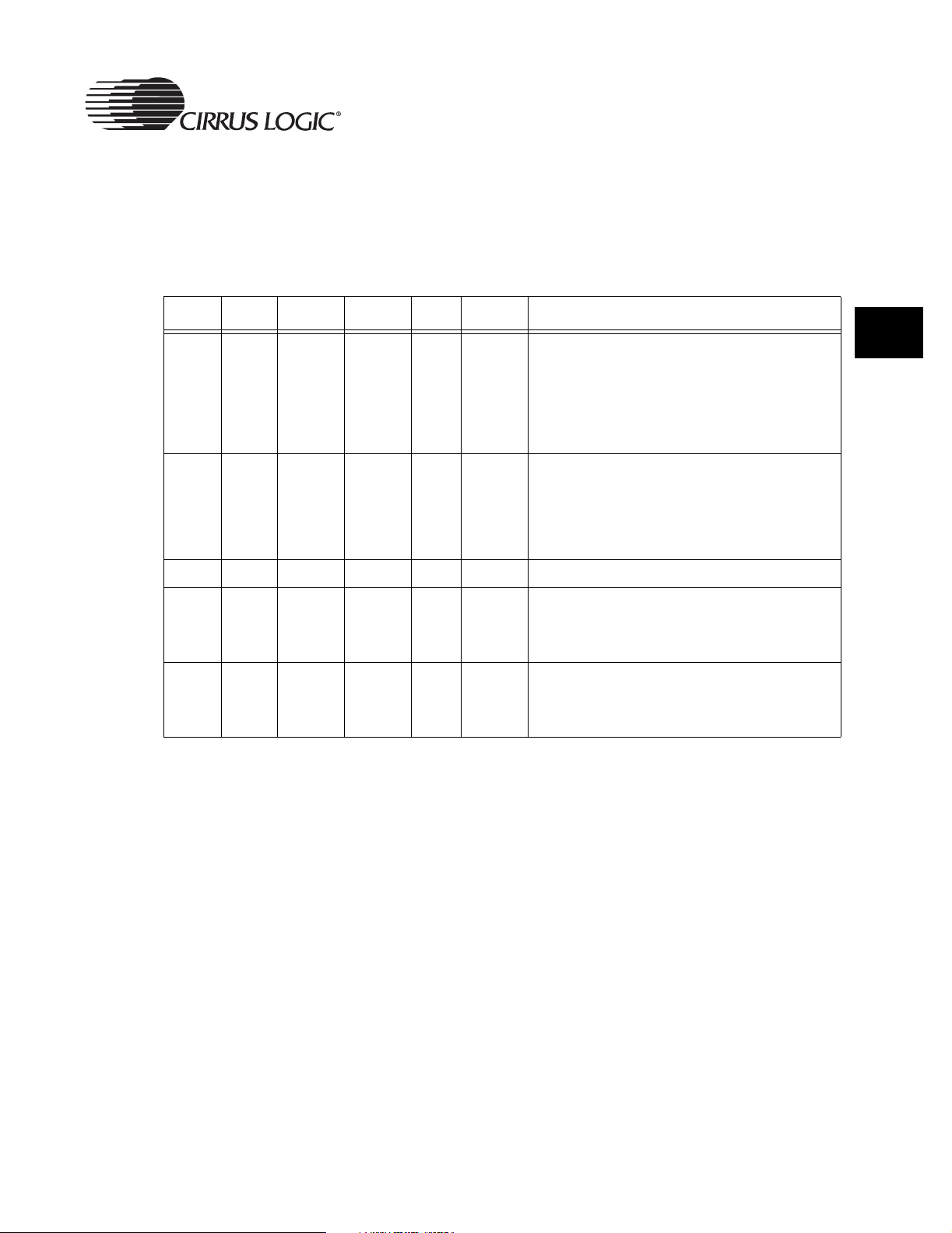
In either normal boot or serial boot mode, once the chip starts up, it will begin
to execute the instruction at logical address 0x0000_0000. Various
configuration options are provided to select the different memory elements for
booting from location 0. The options are listed in Table 4-1.
Table 4-1: Boot Configuration Options
EECLK EEDAT LBOOT1 LBOOT0 ASDO CSn[7:6] Boot Configuration
System Controller
QQ
External boot from Sync memory space selected by
DevCfg3 through the SDRAM Controller. The media
type must be either SROM or SyncFLASH. The
01 0 01
0 0
0 1
01 0 00
0 0
0 1
1 1 0 1 x 01 16-bit serial boot
11 0 01
11 0 00
0 0
0 1
0 0
0 1
selection of the SRAM width is determined by latched
CSn[7:6] value:
16-bit SFLASH
16-bit SROM
External boot from Async memory space selected by
nCS0 through Synchronous Memory Controller. The
selection of the SRAM width is determined by latched
CSn[7:6] value:
8-bit SRAM
16-bit SRAM
Internal boot from on-chip R OM. The selection of the
ROM width is determined by latched
16-bit
16-bit
Internal boot from on-chip R OM. The selection of the
ROM width is determined by latched
8-bit
16-bit
4.1.4 Software System Configuration Options
4
CSn[7:6] value:
CSn[7:6] value:
There are several system configuration options selectable by the DeviceCfg
and SysCfg registers. These registers provide the selection of several pin
multiplexing options and also provide software access to the system reset
configuration options. Please refer to the descriptions of the registers,
“DeviceCfg” on page 91 and “SysCfg” on page 97, for a detailed explanation.
4.1.5 Clock Control
The device uses a flexible system to generate the required clocks. The goal of
the clock system is to generate as many as 20 independent clock frequencies,
some with very tight accuracy requirements, all from a single external lowfrequency crystal or other external clock source. The system was designed so
that once it has been configured, the processor speed and bus speeds can be
set to a number of different speeds without affecting the speeds of the other
clocks in the system.
EP9301 User’s Manual - DS636UM2 69
Copyright 2004 Cirrus Logic
Page 70
4
System Controller
4.1.5.1 Oscillators and Programmable PLLs
The device has an interface to two external crystal oscillators with the
frequency of 32 kHz and 14.7456 MHz. To generate the required highfrequency clocks, the system uses two phase-locked-loops (PLLs) to multiply
the incoming 14.7456 MHz low frequency signal to much higher frequencies
(up to about 400 MHz) that are then divided down by programmable dividers
to produce the needed clocks. The PLLs operate independently of one
another.
The system is split into two “trunks”, each of which is driven by one of the
PLLs. The processor and bus clocks are derived from trunk 1 (PLL1). The
USB and FIR clocks are derived from trunk 2 (PLL2). Other low-frequency
clocks are divided from the original crystal frequency. The MIR and audio
clocks can be independently sourced from either trunk. Figure 4-1, below,
shows the PLL1 structure used in the EP9301. Since PLL2 is identical to
PLL1, wherever the phrase of “PLL1” is used in the figure, it applies to PLL2
as well.
Figure 4-1. Phase Locked Loop (PLL) Structure
14.7456
MHz
PLL1_X1
Feedback Divider
PLL1_X1FBD
Both PLLs are software programmable (each value is defined in ClkSet1 and
ClkSet2 registers respectively). The frequency of output clock Fout shows in
the next equation:
Fout 14.7456M Hz
Here PLL1_X1FBD, PLL1_X2FBD, PLL1_X2IPD and PLL1_PS are the bit
fields in ClkSet1 register. The user must be aware of the requirements of PLL
operation. They are:
Input Divider
PLL1_X2IPD
PLL1_X1FBD 1+()PLL1_X2FBD 1+()×
------- ------------- ------------ ------------- ------------ ------------- --------- ------------ ------------- --
⋅=
PLL1_X2
Feedback Divider
PLL1_X2FBD
PLL1_X2IPD 1+()2
×
2^(PLL1_PS)
PLL1_PS
Fout
• PLL1_X1 desired reference clock frequency range is > 11.058 MHz and <
166 MHz
• PLL1_X1 output frequency range is > 294 MHz and < 368 MHz
70 EP9301 User’s Manual - DS636UM2
Copyright 2004 Cirrus Logic
Page 71
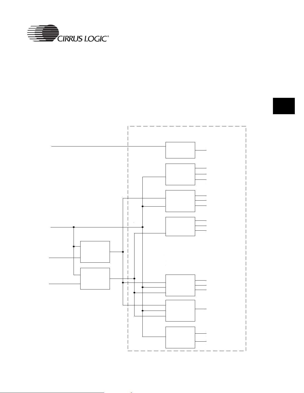
• PLL1_X2 desired reference clock frequency (after PLL1_X2IPD divider) is
> 12.9 MHz and < 166 MHz.
• PLL1_X2 output, BEFORE the PS divide, must be > 290 MHz and <=
528 MHz
Again, the same conditions are applied to PLL2 as well.
4.1.5.2 Bus and Peripheral Clock Generation
System Controller
QQ
Figure 4-2 illustrates the clock generation system.
Figure 4-2. EP9301 Clock Generation System
32 kHz Oscillator
14.7456MHz Oscillator
PLL1 CFG
PLL1
Syscon
32 kHz
Divide
Peripheral
Clocks
CPU and
Bus Clocks
USB and
FIR Clocks
4
W ATCH_CLK
UARTxCLK
SSPCLK
Timer Clocks
FCLK
HCLK
PCLK
USBHost48MHz
USBHost12MHz
FIR_CLK
PLL2 CFG
PLL2
Audio
Clocks
MIR
Clock
ADC
Clock
SCLK
LRCLK
MCLK
MIR_CLK
ADC_CLK
FILT_CLK
EP9301 User’s Manual - DS636UM2 71
Copyright 2004 Cirrus Logic
Page 72
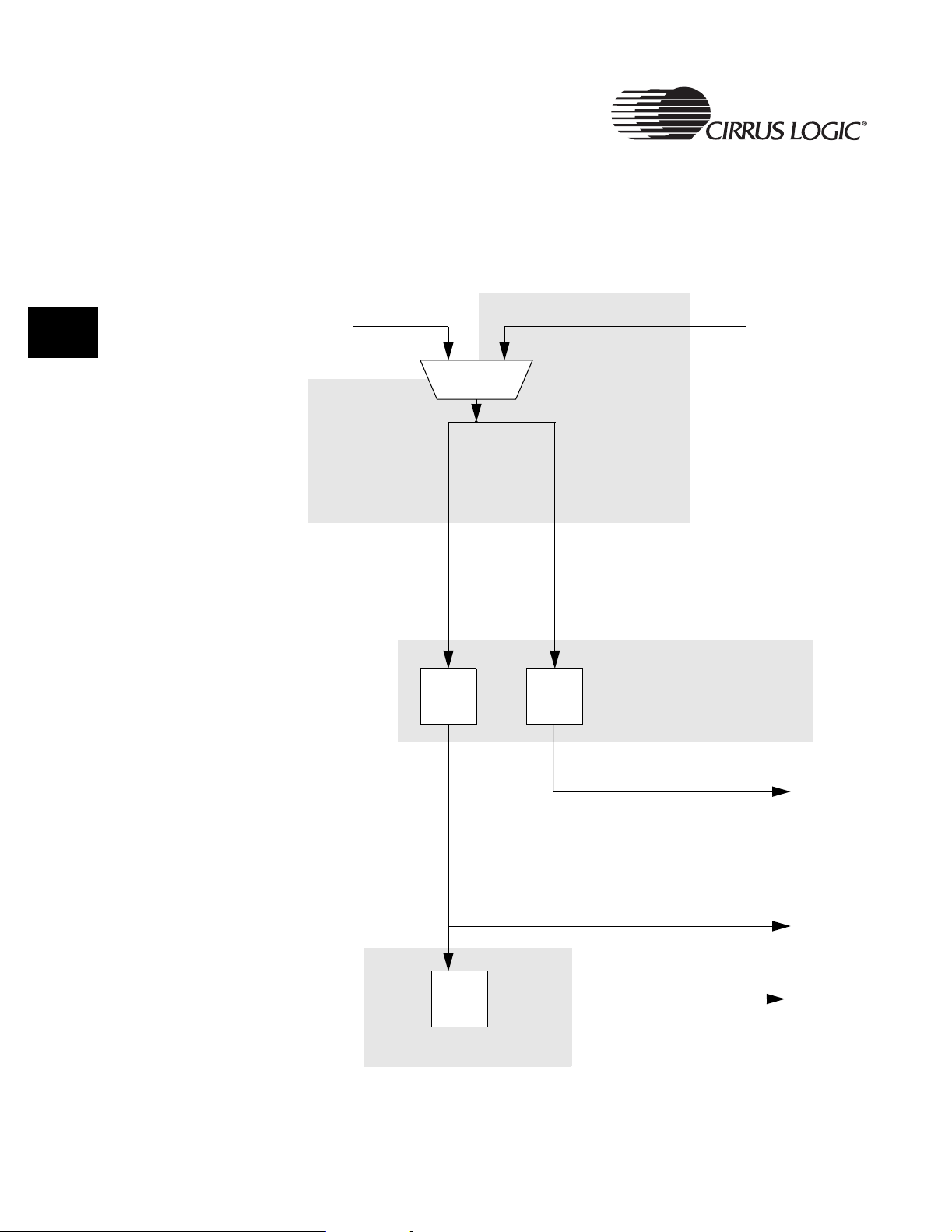
System Controller
4.1.5.2.1 Bus Clock Generation
Figure 4-3 shows the flow of generated system bus clocks, including the ARM
processor clock (FCLK), the AHB bus clock (HCLK), and the APB bus clock
(PCLK).
Figure 4-3. Bus Clock Generation
PLL1External Clock
4
MAX = 66 MHz
HCLK
Div
MAX = 528 MHz
MAX = 166 MHz
For 2nd stage dividers:
FCLK
Div
FCLK Divide = 1, 2, 4, 8, 16
HCLK Divide = 1, 2, 4, 5, 6,
8, 16, 32
FCLK
HCLK
PCLK
Div
PCLK Divide = 1, 2, 4, 8
72 EP9301 User’s Manual - DS636UM2
MAX = 50 MHz
Copyright 2004 Cirrus Logic
PCLK
Page 73

System Controller
There are some limitations of each clock. FCLK must be <=166 MHz,
HCLK<=66 MHz and PCLK<=50 MHz and FCLK >= HCLK > PCLK. Refer to
register, “ClkSet1” on page 84, for the detailed configuration information
regarding the divider bit fields.
It also must be pointed out that even though FCLK is the ARM processor
clock, the ARM Processor has the option to run the CPU using HCLK. The
ARM9 Processor supports three different clocking modes:
QQ
• Async mode
• Sync mode
• Fast Bus mode
Both Async mode and Sync mode use FCLK and potentially FCLK can be
faster than HCLK which would yield higher CPU performance. Async mode
and Sync mode have different clock skew requirements between FCLK and
HCLK, associated with different throughput penalties due to the clock
synchronization. Fast Bus mode bypasses FCLK, and the ARM runs from
HCLK. In this mode, the ARM potentially has lower performance than the
other two modes. When the device starts up, it defaults to Fast Bus mode.
(The selection of ARM clocking modes is determined by the iA and nF bits in
the ARM co-processor 15 register 1.)
4.1.5.2.2 Peripheral Clock Generation
The MCLK and MIR_CLK generators are identical blocks. Each block contains
a pre-divider of 2, 2.5 and 3 followed by a 7-bit programmer divider. The audio
clocks SCLK and LRCLK are further divided down from MCLK. The registers,
“MIRClkDiv” on page 93 and “I2SClkDiv” on page 94, show the details.
USB uses a 48 MHz clock generated by PLL2. USBDIV, in register ClkSet2, is
used to divide the frequency down from the PLL2 output.
4
Table 4-2 on page 74 describes the speeds and sources for the various clocks
on the EP9301.
EP9301 User’s Manual - DS636UM2 73
Copyright 2004 Cirrus Logic
Page 74

4
System Controller
Table 4-2: Clock Speeds and Sources
Block Clocks Used Clock Source
SSP 7.3728 MHz Divided by 2 from 14.7456 MHz external oscillator.
UART1
UART2
AAC 2.9491 MHz Divided-by-5 from the 14.7456MHz external oscillator.
Time rs
Watchdog 256 Hz Tap from the 32 kHz RTC clock.
14.7456 MHz
7.3728 MHz
508.4689 KHz
1.9939 KHz
983 KHz
4.1.5.3 Steps for Clock Configuration
The following is a step-by-step procedure for configuring the clocks. The boot
ROM contains code which performs the following steps for a 14.7456 MHz
crystal. (For details, refer to Boot ROM, Chapter 3 on page 59.) The actual
register values should be taken from the register descriptions for the desired
clock setup.
Both are derived from 14.7456 MHz external oscillator.
All divided by the 14.7456 MHz external oscillator.
1. After power up, the reset state of all clock control registers (all bits zero) will
ensure that FCLK and HCLK are running at the crystal oscillator frequency
(14.7456 MHz).
2. Configure PLL1 to multiply by the desired value, set HCLK and FCLK rates,
and power it up. To do this: write the proper value (taken from the register
table) to ClkSet1 immediately followed by 5 NOP instructions to flush the
ARM920T instruction pipeline. The system will go into Standby while PLL1
stabilizes, then return to normal operation at the new clock rates.
3. Configure PLL2 to multiply by the desired value. To do this, write the proper
value to ClkSet2.
4. Wait for PLL2 to stabilize (at least 1 ms).
Note: The PWRSts register can be checked to confirm the PLLs are locked.
5. Program all other clock dividers to the desired values and enable them.
The clocks won’t actually begin running until the trunks which feed them
are enabled later. Write to the following registers:
• MIRClkDiv
•I2SClkDiv
• ADCClkDiv
6. All peripherals are now running from divided PLL outputs. Once the clocks
have been configured, the frequency of any peripheral clock can be
changed on-the-fly. To do this, perform a write to the clock register with the
74 EP9301 User’s Manual - DS636UM2
Copyright 2004 Cirrus Logic
Page 75

new divisor value and then set the appropriate enable bit. This ensures a
problem-free change of the clock.
4.1.6 Power Management
The device follows a power-saving design plan. Power management is done
by either altering the PLLs or the clock system frequency or by shutting off
clocks to unused blocks. Also, there are several system power states to which
the device can transition in order to save power. Care must be taken to ensure
the clock system is not put into a non-operational state and that clock system
dependencies are observed.
4.1.6.1 Clock Gatings
The list of peripherals with PCLK gating is shown Table 4-3. One should refer
to the appropriate chapters in this User’s Manual to find detailed information
about clock gatings for that peripheral.
Table 4-3: Peripherals with PCLK gating
System Controller
QQ
4
Peripheral
UART1 x --
UART2
IRDA
SEC
I2S
Watchdog - -
AAC x --
SSP
RTC - -
GPIO - x -
The HCLK going to USB Host can be gated off as well to further save the
power. The USH_EN bit in PwrCnt register serves the purpose.
4.1.6.2 System Power States
The device has three power states:
• Run mode: Normal operation mode.
• Halt: ARM9 Processor stops executing.
Peripheral/PCLK
on with Enable or
Register Access
x --
x --
x --
x --
x --
PCLK on with
Register Access
Only
PCLK Continuous
x
x
• Standby: Power is on. Only SDRAM self-refresh and RTC run.
Figure 4-4 illustrates the transitions among those states.
EP9301 User’s Manual - DS636UM2 75
Copyright 2004 Cirrus Logic
Page 76

System Controller
Figure 4-4. EP9301 Power States and Transitions
Power on
Reset
4
Standby Run Halt
4.1.6.2.1 Power-on-Reset Run
During power-on-reset, the chip automatically transition into the run mode.
4.1.6.2.2 Run Standby Mode
Once in the running mode, it is possible to move to the Standby state under
the following conditions:
• A read from the Standby register when SHena bit in register DeviceCfg is
set to 1. This triggers the system to enter STANDBY mode.
• A write to the ClkSet1 register.
When the SHena bit is set to 1 and the user tries to read from the Standby
location, the device is forced into the Standby state. After this transition the
state controller will hold the Standby state before re-loading and allowing the
transition to the operating state.
Read Standby register &
SHena = 1
Write to
ClkSet1 register
Interrupt (if enabled) or
return from ClkSet1
Any Enabled Interrupt
Read Halt register
& SHena = 1
A write to the ClkSet1 register will also trigger the system to go into Standby
mode. However, the system will automatically come back to normal operation
after new clock settings take effect. The amount of time EP9301 remains in
the Standby state depends on whether the PLL is enabled, or if EP9301 is
using the external clock. If the PLL is enabled, EP9301 will remain in Standby
until the PLL is locked. If EP9301 is in PLL bypass mode (nBYP1 = 1), then
EP9301 will remain in the Standby state for 1-2 of the 16.384 kHz clock
cycles. This is to ensure a minimum 'off' time. The 16.384 kHz clock, derived
from the 32 kHz divide chain times how long the system, remains in the
Standby state.
When the device normally enters Standby mode, the SDRAM controller puts
the SDRAM into self-refresh before disabling the clocks. This condition is only
76 EP9301 User’s Manual - DS636UM2
Copyright 2004 Cirrus Logic
Page 77

true if the refresh enable bit (RFSHEN) in the SDRAM controller is set. One
example of this is when a power-on-reset is applied and this register bit is
cleared. This means that this bit will not be set on bootup and will have to be
set to maintain the memory image for when the device re-enters Standby
mode.
4.1.6.2.3 RUN HALT mode
A transition from Run mode to Halt mode is caused by reading the Halt
location with the SHena bit set to 1. This has the effect of gating the processor
clock (FCLK) bus interface, with the APB/AHB system clock, and
Memory/DMA system remaining enabled.
4.1.6.2.4 STANDBY RUN mode
There are normally several conditions in which the device can move from
Standby mode to Run mode.
These conditions are:
System Controller
QQ
4
• A falling edge on Nirq - Global IRQ interrupt
• A falling edge on Nfiq - Global FIQ interrupt
• An exit from a ClkSet1 write
•PRSTn
•RSTOn
The chip comes out of Standby if an interrupt occurs or when an exit from a
ClkSet1 write occurs. If a write is performed to the ClkSet1 register, the
EP9301 will enter Standby and then will automatically come out of Standby
and back into the Run state.
4.1.6.2.5 HALT RUN mode
The transition from the Halt state to the running state is caused by:
• a falling edge on Nirq - Global IRQ interrupt
• a falling edge on Nfiq - Global FIQ interrupt
• RSTOn
4.1.7 Interrupt Generation
The Syscon block generates two interrupts: TICK interrupt and Watchdog
Expired interrupt.
The block generates the TICK interrupt based upon the 64 Hz clock which is
derived from the 32 kHz oscillator. The interrupt becomes active on every
rising edge of the internal 64 Hz clock signal. It can be cleared by writing to the
TEOI location.
EP9301 User’s Manual - DS636UM2 77
Copyright 2004 Cirrus Logic
Page 78

4
System Controller
Watchdog Expired interrupt becomes active on a rising edge of the 64 Hz
TICK clock, if the TICK interrupt is still active. In other words, if a TICK
interrupt has not been served for a complete TICK period, a watchdog expired
interrupt is generated. It can be cleared by writing to the TEOI location as well.
78 EP9301 User’s Manual - DS636UM2
Copyright 2004 Cirrus Logic
Page 79

4.2 Registers
This section contains the detailed register descriptions for registers in the
Syscon block. Table 4-4 shows the address map for the registers in this block,
followed by a detailed listing for each register.
Table 4-4: Syscon Register List
Address Name SW Locked Type Size Description
System Controller
QQ
0x8093_0000 PwrSts No R 32 Power/state control state
0x8093_0004 PwrCnt No R/W 32 Clock/Debug control status
0x8093_0008 Halt No R 32 Reading this location enters Halt mode.
0x8093_000C Standby No R 32 Reading this location enters Standby mode.
0x8093_0018 TEOI No W 32 Write to clear Tick interrupt
0x8093_001C STFClr No W 32
0x8093_0020 ClkSet1 No R/W 32 Clock speed control 1
0x8093_0024 ClkSet2 No R/W 32 Clock speed control 2
0x8093_0040 ScratchReg0 No R/W 32 Scratch register 0
0x8093_0044 ScratchReg1 No R/W 32 Scratch register 1
0x8093_0050 APBWait No R/W 32 APB wait
0x8093_0054 BusMstrArb No R/W 32 Bus Master Arbitration
0x8093_0058 BootModeClr No W 32 Boot Mode Clear register
0x8093_0080 DeviceCfg Yes R/W 32 Device configuration
0x8093_0084 - - - - Reserved
0x8093_0088 MIRClkDiv Yes R/W 32
0x8093_008C I2SClkDiv Yes R/W 32 I2S Audio Clock Divider
Write to clear CLDFLG, RSTFLG and
WDTFLG.
MIR Clock Divider, divides MIR clock for
MIR IrDA
4
0x8093_0090 ADCClkDiv Yes R/W 32 ADC Clock Divider
0x8093_0094 ChipID Yes R/W 32 Chip ID Register
0x8093_009C SysCfg Yes R/W 32 System Configuration
0x8093_00A0 - - - - Reserved
0x8093_00C0 SysSWLock No R/W 1 bit Software Lock Register
EP9301 User’s Manual - DS636UM2 79
Copyright 2004 Cirrus Logic
Page 80
System Controller
Register Descriptions
PwrSts
31 30 29 28 27 26 25 24 23 22 21 20 19 18 17 16
CHIPMAN CHIPID
4
151413 121110 9 8 7 6 543210
WDTFLG RSVD CLDFLG TEST_
RESET
RSTFLG SW _
RESET
PLL2_
LOCK_REG
PLL2_
LOCK
PLL1_
LOCK_REG
PLL1_
LOCK
RTCDIV
Address:
0x8093_0000 - Read Only
Definition:
The PwrSts system control register is the Power/State control register.
Bit Descriptions:
RSVD: Reserved. Unknown During Read.
RTCDIV: The 6-bit RTCDIV shows the number of 64-seconds which
have elapsed. It is the output of the divide-by-64 chain that
divides the 64 Hz TICK clock down to 1 Hz though
showing an incrementing count. The MSB is the 1 Hz
output; the LSB is the 32 Hz output. It is reset by poweron-reset to 000000b.
PLL1_LOCK: PLL1 lock. This signal goes high when PLL1 is locked and
it is at the correct frequency.
PLL1_LOCK_REG:Registered PLL1 lock. This is a one-shot registered signal
of the PLL1_LOCK signal. It is only cleared on a poweron-reset, when EP9301 enters the Standby state or when
PLL1 is powered down.
PLL2_LOCK: PLL2 lock. This signal goes high when PLL2 is locked, and
it is at the correct frequency.
PLL2_LOCK_REG:Registered PLL2 lock. This is a one-shot registered signal
of the PLL2_LOCK signal. It is only cleared on a poweron-reset, when ClkSet2 is written, EP9301 enters the
Standby state, or PLL2 is powered down.
SW_RESET: Software reset flag. This bit is set if the software reset has
been activated. It is cleared by writing to the STFClr
location. On power-on-reset, it is reset to 0b.
80 EP9301 User’s Manual - DS636UM2
Copyright 2004 Cirrus Logic
Page 81

System Controller
RSTFLG: Reset flag. This bit is set if the user reset button has been
pressed; forcing the RSTOn input low. It is cleared by
writing to the STFClr location. On power-on-reset, it is
reset to 0b.
TEST_RESET: Test reset flag. This bit is set if the test reset has been
activated; it is cleared by writing to the STFClr location. On
power-on-reset, it is reset to 0b.
QQ
CLDFLG: Cold start flag. This bit is set if EP9301 has been reset
with a power-on-reset; it is cleared by writing to the STFClr
location. On power-on-reset, it is set to 1b.
WDTFLG: Watchdog Timer flag. This bit is set if the Watchdog timer
resets the system. It is cleared by writing to the STFClr
location. It is reset to 0.
CHIPID: Chip ID bits. This 8-bit register determines the Chip
Identification for EP9301. For EP9301, this value is 0x20.
CHIPMAN: This 8-bit register determines the Chip Manufacturer ID for
EP9301. For EP9301, this value is 0x43.
PwrCnt
31 30 29 28 27 26 25 24 23 22 21 20 19 18 17 16
FIR_EN RSVD UART
15 14 13 12 11 10 9 8 7 6 5 4 3 2 1 0
BAUD
USH_EN DMA
M2M
CH1
DMA
M2M
CH0
DMA
M2P
CH8
DMA
M2P
CH9
RSVD
DMA
M2P
CH6
DMA
M2P
CH7
DMA
M2P
CH4
DMA
M2P
CH5
DMA
M2P
CH2
DMA
M2P
CH3
DMA
M2P
CH0
DMA
M2P
CH1
4
Address:
0x8093_0004 - Read / Write
Definition:
The PwrCnt system control register is the Clock/Debug control status register.
Bit Descriptions:
RSVD: Reserved. Unknown During Read.
EP9301 User’s Manual - DS636UM2 81
Copyright 2004 Cirrus Logic
Page 82

4
System Controller
DMA M2M/P CHx: These bits enable the clocks to the DMA controller
channels. Note that a channels-enable bit MUST be
asserted before any register within the DMA controller can
be read or written. At least one ARM instruction cycle must
occur between writing to this register to enable the DMA
Controller channel and actually accessing it. The number
of cycles will depend on the setting of HCLK and PCLK
division in the ClkSetx register. To save power, ensure that
all these bits are disabled (low) if the DMA controller is not
being used. On a system reset, the register will be reset to
zero.
USH_EN: This bit is used to gate the HCLK to the USB Host block in
order to save power. It is reset to zero, thus gating off the
HCLK. It can be set to one to turn on the HCLK to the USB
Host. This bit must be set before any register within the
USB Host can be accessed. At least one ARM instruction
cycle must occur between writing to this register bit and
actually accessing the USB Host. The number of cycles
will depend on the setting of HCLK and PCLK division in
the ClkSetx register.
This bit is also used to gate the 48 MHz and 12 MHz
clocks to the USB Host block in order to save power. It is
reset to zero, thus gating off the USB Host clocks. By
setting this to one, the USB Host clocks are enabled. At
least one ARM instruction cycle must occur between
writing to this register bit and actually accessing the USB
Host. The number of cycles will depend on the wake-up
time for PLL2. To find out if PLL2 has locked on to its
frequency, the PLL2_LOCK bit in the PwrSts register can
be read.
UARTBAUD: This bit controls the clock input to the UARTs. When
cleared, the UARTs are driven by the 14.7456 MHz clock
divided by 2 (7.3728 MHz). This gives a maximum baudrate of 230 Kbps. When set, the UARTs are driven by the
14.7456 MHz clock directly, giving an increased maximum
baud rate of 460 Kbps. This bit is 0 on reset.
FIR_EN: This bit is used to gate the FIRCLK to the IrDA block in
order to save power. It is reset to zero, thus gating off the
FIRCLK. Setting this bit to one will turn on the 48 MHz
clock to the IrDA.
82 EP9301 User’s Manual - DS636UM2
Copyright 2004 Cirrus Logic
Page 83
System Controller
Standby and Halt
31 30 29 28 27 26 25 24 23 22 21 20 19 18 17 16
RSVD
15 14 13 12 11 10 9 8 7 6 5 4 3 2 1 0
RSVD
Address:
Standby - 0x8093_000C - Read Only
Halt - 0x8093_0008 - Read Only
Definition:
The Standby and Halt registers allow entry into the power saving modes. A
read to the Halt location will initiate a request for the system to enter Halt
mode, if the SHena bit is set in the DeviceCfg register in Syscon. Likewise a
read to Standby will request entry into Standby only when the SHena bit is set.
QQ
4
Note: When a read is performed to the Standby location, it must be immediately
followed by 5 NOP instructions. This is needed to flush the instruction pipeline in
the ARM920T core. Writes to these locations have no effect.
Bit Descriptions:
RSVD: There are no readable bits in this register.
TEOI
31 30 29 28 27 26 25 24 23 22 21 20 19 18 17 16
RSVD
15 14 13 12 11 10 9 8 7 6 5 4 3 2 1 0
RSVD
Address:
0x8093_0018 - Write
Definition:
Writing to the TEOI location will clear the periodic Watchdog expired interrupt
(WEINT) and the 64 Hz TICK interrupt (TINT). Any data written to the register
triggers the clearing.
Bit Descriptions:
RSVD: There are no readable bits in this register.
EP9301 User’s Manual - DS636UM2 83
Copyright 2004 Cirrus Logic
Page 84
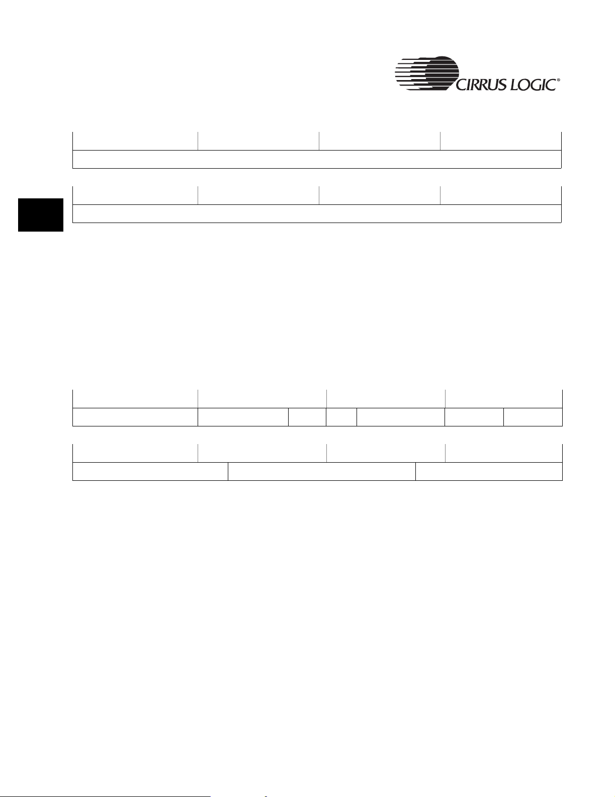
4
System Controller
STFClr
31 30 29 28 27 26 25 24 23 22 21 20 19 18 17 16
RSVD
15 14 13 12 11 10 9 8 7 6 5 4 3 2 1 0
RSVD
Address:
0x8093_001C - Write
Definition:
Writing to the STFClr location will clear the CLDFLG, WDTFLG and RSTFLG
in the register, “PwrSts” on page 80. Any data written to the register triggers
the clearing.
Bit Descriptions:
RSVD: There are no readable bits in this register.
ClkSet1
31 30 29 28 27 26 25 24 23 22 21 20 19 18 17 16
RSVD FCLK DIV SMC ROM nBYP1 HCLK DIV PCLK DIV PLL1_PS
1514131211109 8 76543210
PLL1 X1FBD1 PLL1 X2FBD2 PLL1 X2IPD
Address:
0x8093_0020 - Read/Write
Definition:
The ClkSet1 system control register is one of two register that control clock
speeds.
Note: When a write is performed to the ClkSet1 location, it must be immediately
followed by 5 NOP instructions. This is needed to flush the instruction pipeline in
the ARM920T core. Writing to this register will cause the EP9301 to enter
Standby for between 8 ms to 16 ms. Reading from this register will not cause an
entry into Standby mode.
Bit Descriptions:
RSVD: Reserved. Unknown During Read.
PLL1_X2IPD: These 5 register bits set the input divider for PLL1
operation. On power-on-reset the value is set to 00111b (7
decimal).
84 EP9301 User’s Manual - DS636UM2
Copyright 2004 Cirrus Logic
Page 85

System Controller
Note: The value in the register is the actual coefficient minus one.
PLL1_X2FBD2: These 6 register bits set the first feedback divider bits for
PLL1. On power-on-reset the value is set to 000111b (7
decimal).
Note: The value in the register is the actual coefficient minus one.
PLL1_X1FBD1: These 5 register bits set the second feedback divider bits
for PLL1. On power-on-reset the value is set to 10011b (19
decimal).
Note: The value in the register is the actual coefficient minus one.
PLL1_PS: These two bits determine the final divide on the VCO clock
signal in PLL1.
00 - Divide by 1
01 - Divide by 2
10 - Divide by 4
11 - Divide by 8
QQ
4
On power-on-reset these bits are reset to 11b (3 decimal).
Note: This means that PLL1 FOUT is programmed to be 36,864,000 Hz on startup.
Note: The value in the register is the actual coefficient minus one.
PCLKDIV: These two bits set the divide ratio between the HCLK AHB
clock and the APB clock (PCLK)
00 - Divide by 1
01 - Divide by 2
10 - Divide by 4
11 - Divide by 8
On power-on-reset the value is set to 00b.
Note: Care must be taken to make the correct selection of PCLK divide for the HCLK
frequency used, so that the required minimum ratio between PCLK and the
peripheral clock is not violated
HCLKDIV: These three bits set the divide ratio between the VCO
output and the bus clock (HCLK)
000 - Divide by 1 100 - Divide by 6
001 - Divide by 2 101 - Divide by 8
010 - Divide by 4 110 - Divide by 16
011 - Divide by 5 111 - Divide by 32
On power-on-reset the value is set to 000b.
EP9301 User’s Manual - DS636UM2 85
Copyright 2004 Cirrus Logic
Page 86
4
System Controller
nBYP1: This bit selects the clock source for the processor clock
dividers. With this bit clear, the system wakes up and
boots with the PLL bypassed and uses an external clock
source. With nBYP1 set, the system runs with the PLL
generated clock. The default for this bit is to boot/run from
external clock source.
SMCROM: If set, this bit will gate off the HCLK to the Static Memory
Controller when in Halt mode and therefore save power.
When in Halt mode, there are no Instruction Code fetches
occurring and therefore if there are no DMA operations in
progress that may require the SMC, there will be no
accesses to this controller. It may therefore be safely
disabled when in Halt mode. This bit is 0b on reset.
FCLKDIV: These three bits set the divide ratio between the VCO
output and processor clock. On power-on-reset the value
is set to 000b.
000 - Divide by 1 011 - Divide by 8
001 - Divide by 2 100 - Divide by 16
010 - Divide by 4
For FCLKDIV values equal to 1xxb (except for 100b), the
divide ratio will be divide by 1.
ClkSet2
31 30 29 28 27 26 25 24 23 22 21 20 19 18 17 16
USB DIV RSVD nBYP2 PLL2_EN PLL2_PS
15 14 13 12 11 10 9 8 7 6 5 4 3 2 1 0
PLL2 X1FBD1 PLL2 X2FBD2 PLL2 X2IPD
Address:
0x8093_0024 - Read/Write
Definition:
The ClkSet2 register is used for setting the dividers internally to PLL2 and to
the USB Host divider. The reset setting for PLL2 creates a frequency of
48 MHz. The default divider for USB_DIV is divide by 1, which will produce the
USB host clock frequency and FIR clock frequency of 48 MHz.
Bit Descriptions:
PLL2_X2IPD: These 5 register bits set the input divider for PLL2
operation. On power-on-reset the value is set to 10111b
(23 decimal).
Note: The value in the register is the actual coefficient minus one.
86 EP9301 User’s Manual - DS636UM2
Copyright 2004 Cirrus Logic
Page 87

System Controller
PLL2_X2FBD2: These 6 register bits set the first feedback divider bits for
PLL2. On power-on-reset the value is set to 11000b (24
decimal).
Note: The value in the register is the actual coefficient minus one.
PLL2_X1FBD1: These 5 register bits set the second feedback divider bits
for PLL2. On power-on-reset the value is set to 11000b (24
decimal).
Note: The value in the register is the actual coefficient minus one.
PLL2_PS: These two bits determine the final divide function on the
VCO clock signal in PLL2.
00 - Divide by 1
01 - Divide by 2
10 - Divide by 4
11 - Divide by 8
On power-on-reset these bits are reset to 11b (3 decimal).
QQ
4
Note: This means that PLL2 FOUT is programmed to be 48,000,000 Hz on startup.
Note: The value in the register is the actual coefficient minus one.
PLL2_EN: This bit enables PLL2. If set, PLL2 is enabled. If this bit is
zero, PLL2 is disabled. On power-on-reset the value is set
to 0b.
nBYP2: This bit selects the clock source for the processor clock
dividers. If set, PLL2 is the clock source. If this bit is set to
zero, the external clock is the clock source. On power-onreset, this bit defaults to 0b.
USBDIV: These four bits set the divide ratio between the PLL2
output and the USB clock.
0000 - Divide by 1 1000 - Divide by 9
0001 - Divide by 2 1001 - Divide by 10
0010 - Divide by 3 1010 - Divide by 11
0011 - Divide by 4 1011 - Divide by 12
0100 - Divide by 5 1100 - Divide by 13
0101 - Divide by 6 1101 - Divide by 14
0110 - Divide by 7 1110 - Divide by 15
0111 - Divide b y 8 1111 - Divide by 1
On power-on-reset these bits are reset to 0000b.
EP9301 User’s Manual - DS636UM2 87
Copyright 2004 Cirrus Logic
Page 88

4
System Controller
ScratchReg0, ScratchReg1
31 30 29 28 27 26 25 24 23 22 21 20 19 18 17 16
Val ue
1514131211109876543210
Val ue
Address:
ScratchReg0 - 0x8093_0040, Read/Write
ScratchReg1 - 0x8093_0044, Read/Write
Default:
0x0000_0000
Definition:
Each of these locations provide a 32-bit read/write scratch register, that can be
used as a general purpose storage. These registers are reset to zero only on a
power-on-reset. A System Reset will have no effect.
Bit Descriptions:
Value: This is a 32-bit read/write location.
APBWait
31 30 29 28 27 26 25 24 23 22 21 20 19 18 17 16
RSVD
15 14 13 12 11 10 9 8 7 6 5 4 3 2 1 0
RSVD NO_WRITE_WAIT
Address:
0x8093_0050, Read/Write
Definition:
The APBWait register controls the insertion of wait states for APB peripherals.
Bit Descriptions:
RSVD: Reserved. Unknown During Read.
NO_WRITE_WAIT:Used in the AHB/APB bridge to not insert an AHB wait
during writes, if set. If reset, a wait state is added by
forcing HREADY = 0 during ST_WRITE. This bit resets to
0x0001.
88 EP9301 User’s Manual - DS636UM2
Copyright 2004 Cirrus Logic
Page 89
System Controller
BusMstrArb
31 30 29 28 27 26 25 24 23 22 21 20 19 18 17 16
RSVD
15 14 13 12 11 10 9 8 7 6 5 4 3 2 1 0
QQ
RSVD RSVD MAC
Address:
Definition:
Bit Descriptions:
ENFIQ
MAC
ENIRQ
USH
ENFIQ
USH
ENIRQ
DMA_
ENFIQ
DMA_
ENIRQ
PRI
CORE
RSVD PRI_ORD
0x8093_0054 - Read/Write
The Bus Master arbitration register (BusMstrArb) is used to configure the AHB
master priority order.
RSVD: Reserved. Unknown During Read.
PRI_ORD: Used to set the priority of the AHB arbiter. The priority
order is shown below. This field resets to 00.
Priority Number
1 MAC MAC DMA DMA
2 USB USB USB MAC
3 DMA ARM920T MAC USB
4 ARM920T DMA ARM920T ARM920T
PRIOR 00
(Reset value)
PRIOR 01 PRIOR 10 PRIOR 11
PRI_CORE: When this bit is set the Core will become highest priority
following a grant to one of the following: MAC, USB and
DMA. If the Core then requests the bus, it is then placed in
the priority order selected by PRI_ORD after it is granted,
until one of the above masters is granted the bus, and is
placed on top of the priority scheme.
4
DMA_ENIRQ: When set the arbiter will degrant DMA from the AHB bus
and will ignore subsequent requests from DMA if an IRQ is
active. When IRQ is cleared the DMA request is allowed
again. There is no impact on other masters. Reset to 0.
DMA_ENFIQ: When set the arbiter will degrant DMA from the AHB bus
and will ignore subsequent requests from DMA if an FIQ is
active. When FIQ is cleared the DMA request is allowed
again. There is no impact on other masters. Reset to 0.
EP9301 User’s Manual - DS636UM2 89
Copyright 2004 Cirrus Logic
Page 90

4
System Controller
USH_ENIRQ: When set the arbiter will degrant USB host from the AHB
bus and will ignore subsequent requests from the USB
Host if an IRQ is active. When IRQ is cleared, the USB
Host request is allowed again. There is no impact on other
masters. Reset to 0.
USH_ENFIQ: When set the arbiter will degrant USB Host from the AHB
bus and will ignore subsequent requests from USB Host if
an FIQ is active. When FIQ is cleared, the USB Host
request is allowed again. There is no impact on other
masters. Reset to 0.
MAC_ENIRQ: When set the arbiter will degrant Ethernet MAC from the
AHB bus and will ignore subsequent requests from the
MAC if an IRQ is active. When IRQ is cleared, the MAC
request is allowed again. There is no impact on other
masters. Reset to 0.
MAC_ENFIQ: When set the arbiter will degrant the Ethernet MAC from
the AHB bus and will ignore subsequent requests from the
MAC if an FIQ is active. When FIQ is cleared, the MAC
request is allowed again. There is no impact on other
masters. Reset to 0.
BootModeClr
31 30 29 28 27 26 25 24 23 22 21 20 19 18 17 16
RSVD
15 14 13 12 11 10 9 8 7 6 5 4 3 2 1 0
RSVD
Address:
0x8093_0058 - Write Only
Definition:
The BootModeClr register is a write-to-clear register. Reset activates the boot
ROM remap function causing the internal boot ROM to map to address zero, if
internal boot is selected. Writing BootModeClr removes the internal ROM
address remap, restoring normal address space.
Bit Descriptions:
RSVD: There are no readable bits in this register.
90 EP9301 User’s Manual - DS636UM2
Copyright 2004 Cirrus Logic
Page 91
System Controller
DeviceCfg
31 30 29 28 27 26 25 24 23 22 21 20 19 18 17 16
SWRST D1onG D0onG IonU2 1 0 MonG RSVD RSVD 0 0 U2EN RSVD U1EN ADCEN RSVD
15 14 13 12 11 10 9 8 7 6 5 4 3 2 1 0
QQ
0 0 HC1IN H C1EN 1 1 0 1 I2Son
Address:
0x8093_0080 - Read/Write, Software locked
Default:
0x0000_0000
Definition:
Device Configuration Register. This register controls the operation of major
system functions.
Bit Descriptions:
RSVD: Reserved. Unknown During Read.
0: This bit must be written as “0”.
1: This bit must be written as “1”.
SHena: Standby/Halt enable. When 1, allows the system to enter
Standby or Halt on a read from the Standby and Halt
registers, respectively.
ADCPD: ADC Power Down.
1 - ADC and clocks are powered down.
0 - ADC and clocks are active. ADCPD must be zero for
normal ADC operation.
SSP
I2Son
AC97
0 RSVD RSVD ADCPD RSVD SHena
4
ADCEN ADC Enable. The ADCEN bit does not affect the ADC
power state. ADC power down is directly controlled by the
ADCPD bit.
1 = ADC Interface enabled.
0 = ADC Interface disabled.
I2SonAC97: I2S on AC97 pins. The I2S block uses the AC97 pins.
(See Table 4-5 on page 92, below.)
Note: The I2S should be enabled on only one set of pins. Therefore I2SonAc97 and
I2SonSSP are mutually exclusive. Setting both I2SonAc97 and I2SonSSP will
cause unexpected behavior.
EP9301 User’s Manual - DS636UM2 91
Copyright 2004 Cirrus Logic
Page 92

System Controller
I2SonSSP: I2S on SSP pins. The I2S block uses the SSP pins. MCLK
Note: The I2S should be enabled on only one set of pins. Therefore I2SonAc97 and
I2SonSSP are mutually exclusive. Setting both I2SonAc97 and I2SonSSP will
cause unexpected behavior.
Table 4-5: Audio Interfaces Pin Assignment
is not available in this pin option. (See Table 4-5 on page
92, below.)
4
Pin
Name
SCLK1 SPI Bit Clock I2S Serial Clock SPI Bit Clock
SFRM1 SPI Frame Clock I2S Frame Clock SPI Frame Clock
SSPRX1 SPI Serial Input I2S Serial Input SPI Serial Input
SSPTX1 SPI Serial Output I2S Serial Output SPI Serial Output
ARSTn AC'97 Reset AC'97 Reset I2S Master Clock
ABITCLK AC'97 Bit Clock AC'97 Bit Clock I2S Serial Clock
ASYNC AC'97 Frame Clock AC'97 Frame Clock I2S Frame Clock
ASDI AC'97 Serial Input AC'97 Serial Input I2S Serial Input
ASDO AC'97 Serial Output AC'97 Serial Output I2S Serial Output
Normal Mode I2S on SSP Mode I2S on AC'97 Mode
Pin Description Pin Description Pin Description
(No I2S Master Clock)
HC1IN: HDLC1 clock in. This bit has no effect unless HC1EN is 1.
1 = pin EGPIO[3] is an input and drives an external HDLC
clock to UART1.
0 = pin EGPIO[3] is an output driven by UART1.
HC1EN: HDLC1 clock enable.
1 = pin EGPIO[3] is used for an HDLC clock with UART1.
0 = pin EGPIO[3] is not used.
U1EN: UART1 Enable.
1 - UART1 baud rate clock is active.
0 - UART1 clock is off.
U2EN: UART2 Enable.
1 - UART2 baud rate clock is active.
0 - UART2 clock is off.
MonG: Modem on GPIO.
1 - Modem support signals use EGPIO[0] pins.
0 - Modem support signals do not use EGPIO[0] pins
IonU2: IrDA on UART2.
1 - UART2 is used as an IrDA interface,
0 - UART2 is a normal UART.
92 EP9301 User’s Manual - DS636UM2
Copyright 2004 Cirrus Logic
Page 93

System Controller
D0onG: External DMA0 hardware handshake signals mapped to
EGPIO pins.
1 - Signals mapped.
0 - Signals not supported.
D1onG: External DMA1 hardware handshake signals mapped to
EGPIO pins.
1 - Signals mapped.
0 - Signals not supported.
SWRST: Software reset. A one to zero transition of this bit initiates
a software reset.
MIRClkDiv
31 30 29 28 27 26 25 24 23 22 21 20 19 18 17 16
RSVD
QQ
4
15 14 13 12 11 10 9 8 7 6 5 4 3 2 1 0
MENA ESEL PSEL RSVD PDIV RSVD MDIV
Address:
0x8093_0088 - Read/Write, Software locked
Default:
0x0000_0000
Definition:
Configures MIR clock for the MIR IrDA. Selects input to MIR clock dividers
from either PLL1 or PLL2, and defines a programmable divide value.
Bit Descriptions:
RSVD: Reserved. Unknown During Read.
MENA: Enable MIR_CLK divider.
ESEL: External clock source select.
0 - Use the external XTALI clock input as the clock source.
1 - Use one of the internal PLLs selected by PSEL as the
clock source.
PSEL: PLL source select.
1 - Select PLL2 as the clock source.
0 - Select PLL1 as the clock source.
EP9301 User’s Manual - DS636UM2 93
Copyright 2004 Cirrus Logic
Page 94

4
System Controller
PDIV: Pre-divider value. Generates divide by 2, 2.5, or 3 from the
clock source.
00 - Disable clock
01 - Divide-by-2
10 - Divide-by-2.5
11 - Divide-by-3
MDIV: MIR_CLK divider value. Forms a divide-by-N of the pre-
divide clock output. MIR_CLK is the source clock divided
by PDIV divided by N.
I2SClkDiv
31 30 29 28 27 26 25 24 23 22 21 20 19 18 17 16
SENA SLAVE ORIDE RSVD DROP SPOL LRDIV SDIV
15 14 13 12 11 10 9 8 7 6 5 4 3 2 1 0
MENA ESEL PSEL RSVD PDIV RSVD MDIV
Address:
Default:
Definition:
Bit Descriptions:
0x8093_008C - Read/Write, Software locked
0x0000_0000
Configures the I2S block audio clocks MCLK, SCLK, and LRCLK.
RSVD: Reserved. Unknown During Read.
SENA: Enable audio clock generation.
SLAVE: I2S slave. Configures the I2S clock system to operate as a
slave. SCLK and LRCLK are chip inputs. The clock
configuration controls in this register are ignored in slave
mode.
ORIDE: Override I2S master configuration.
1 - Override the SAI_MSTR_CLK_CFG from the I2S block
and use the I2SClkDiv Register settings.
0 - Use the I2S SAI_MSTR_CLK_CFG signals.
DROP: Drop SCLK clocks.
1 - When in 64x mode, drop 8 SCLKs.
0 - Do not drop SCLKs.
94 EP9301 User’s Manual - DS636UM2
Copyright 2004 Cirrus Logic
Page 95

System Controller
SPOL: SCLK polarity. Defines the SCLK edge that aligns to
LRCLK transitions.
1 - LRCLK transitions on the falling SCLK edge.
0 - LRCLK transitions on the rising SCLK edge.
LRDIV: LRCLK divide select.
00 - LRCK = SCLK / 32
01 - LRCK = SCLK / 64
10 - LRCK = SCLK / 128
11 - Reserved
SDIV: SCLK divide select.
1 - SCLK = MCLK / 4,
0 - SCLK = MCLK / 2.
MENA: Enable master clock generation.
ESEL: External clock source select.
0 - Use the external XTALI clock input as the clock source.
1 - Use one of the internal PLLs selected by PSEL as the
clock source.
QQ
4
PSEL: PLL source select.
1 - Select PLL2 as the clock source.
0 - Select PLL1 as the clock source.
PDIV: Pre-divider value. Generates divide by 2, 2.5, or 3 from the
clock source.
00 - Disable clock
01 - Divide-by-2
10 - Divide-by-2.5
11 - Divide-by-3
MDIV: MCLK divider value. Forms a divide-by-N of the pre-divide
clock output. MCLK is the source clock divided by PDIV
divided by N.
ADCClkDiv
31 30 29 28 27 26 25 24 23 22 21 20 19 18 17 16
ADCEN RSVD ADIV
15 14 13 12 11 10 9 8 7 6 5 4 3 2 1 0
RSVD
Address:
0x8093_0090 - Read/Write, Software locked
Default:
EP9301 User’s Manual - DS636UM2 95
Copyright 2004 Cirrus Logic
Page 96
System Controller
Definition:
Bit Descriptions:
0x0000_0000
Configures the ADC clocks.
RSVD: Reserved. Unknown During Read.
ADCEN: ADC clock enable.
4
ADIV: ADC clock divider value.
0 - ADC Clock is divide-by-16 from the external oscillator.
1 - ADC Clock is divide-by-4 from the external oscillator.
CHIP_ID
31 30 29 28 27 26 25 24 23 22 21 20 19 18 17 16
REV RSVD 0 RSVD 0 RSVD
15 14 13 12 11 10 9 8 7 6 5 4 3 2 1 0
ID
Address:
0x8093_0094 - Read Only
Definition:
Chip ID register.
Bit Descriptions:
RSVD: Reserved. Unknown During Read.
REV: Revision: Reads chip Version number:
0000 - Rev A
0001 - Rev B
0010 - Rev C
0011 - Rev D0
0100 - Rev D1
0101 - Rev E0
0: Reads zero.
ID[15:0]: Chip ID Number, reads 9213.
96 EP9301 User’s Manual - DS636UM2
Copyright 2004 Cirrus Logic
Page 97

System Controller
SysCfg
31 30 29 28 27 26 25 24 23 22 21 20 19 18 17 16
REV RSVD
15 14 13 12 11 10 9 8 7 6 5 4 3 2 1 0
RSVD SBOOT LCSn7 LCSn6 LASDO LEEDA LEECLK RSVD LCSn2 LCSn1
Address:
0x8093_009C - Read/Write, Software locked
Default:
0x0000_0000
Definition:
System Configuration Register. Provides various system configuration
options.
QQ
4
Bit Descriptions:
RSVD: Reserved. Unknown During Read.
REV: Revision: Reads chip Version number:
0000 - Rev A
0001 - Rev B
0010 - Rev C
0011 - Rev D0
0100 - Rev D1
0101 - Rev E0
SBOOT: Serial Boot Flag.
1 - hardware detected Serial Boot selection,
0 - hardware detected Normal Boot. This bit is read-only.
LCSn7, LCSn6: Latched version of CSn7 and CSn6 respectively. These
are used to define the external bus width for the boot
code.
LASDO: Latched version of ASDO pin. Used to select synchronous
versus asynchronous boot device.
LEEDA: Latched version of EEDAT pin.
LEECLK: Define Internal or external boot:
1 - Internal
0 - External
EP9301 User’s Manual - DS636UM2 97
Copyright 2004 Cirrus Logic
Page 98

System Controller
SysSWLock
LCSn2, LCSn1: Define Watchdog startup action:
00 - Watchdog disabled, Reset duration disabled
01 - Watchdog disabled, Reset duration active
10 - Watchdog active, Reset duration disabled
11 - Watchdog active, Reset duration active
4
31 30 29 28 27 26 25 24 23 22 21 20 19 18 17 16
RSVD
15 14 13 12 11 10 9 8 7 6 5 4 3 2 1 0
RSVD LOCK
Address:
0x8093_00C0 - Read/Write
Default:
0x0000_0000
Definition:
Syscon Software Lock Register. Provides software control port for all Syscon
locked registers. Writing the LOCK field to 0xAA opens the lock. Reading the
register will return 0x0000_0001 when the lock is open, and all zeros when the
lock is closed (locked).
Bit Descriptions:
RSVD: Reserved. Unknown During Read.
LOCK: Lock code value. This field must be written to a value of
0xAA to open the software lock. Reads 0x01 when the
lock is open, 0x00 when the lock is closed.
98 EP9301 User’s Manual - DS636UM2
Copyright 2004 Cirrus Logic
Page 99

5.1 Introduction
The EP9301 contains two cascade Vectored Interrupt Controllers (VIC). A
Vectored Interrupt has improved latency compared with a simple interrupt
controller, since it provides direct information about where the interrupt’s
service routine is located and eliminates levels of software arbitration.
Each individual Vectored Interrupt Controller can handle up to 32 interrupts,
but there are more than 32 interrupts in this design. Therefore two VICs are
connected in a daisy-chain, which allows the system to handle up to 64
interrupt sources.
R
Chapter 5
5Vectored Interrupt Controller
5
There are up to 16 vectored interrupts and 16 non-vectored interrupts
available on each VIC. Vectored interrupts can only generate an IRQ interrupt.
The vectored and nonvectored Interrupt Requests (IRQ) provide an address
for an Interrupt Service Routine (ISR). Reading from the vector interrupt
address register, VICxVectAddr, provides the address of the ISR, and updates
the interrupt priority hardware that masks out the current and any lower priority
interrupt requests. Writing to the VICxVectAddr register indicates to the
interrupt priority hardware that the current interrupt is serviced, allowing lower
priority interrupts to go active.
Registers in the VIC use a bit position for each different interrupt source. The
bit position is fixed but the handling of each interrupt is configurable by the
VIC. Software can control each request line to generate software interrupts.
The VIC provides a software interface to the interrupt system. In this system,
two levels of interrupt are available:
• Fast Interrupt Request (FIQ) for fast, low latency interrupt handling.
• Interrupt Request (IRQ) for more general interrupts.
All interrupt inputs to the VIC are presented as active-high level sensitive
signals. Any conditioning needed to achieve this is performed by the block
generating the interrupt request. In the case of the external interrupts, the
GPIO block takes care of the conditioning.
EP9301 User’s Manual - DS636UM2 99
Copyright 2004 Cirrus Logic
Page 100
Vectored Interrupt Controller
Figure 5-1. Vectored Interrupt Controller Block Diagram
5
VICINTSO URCE [63:32]
2
VIC1
VICINTSOURCE[31:0]
Vector Address and
Priority Logic
Vector Address and Priority
Vector Addr from VIC1
FIQ from VIC1
IRQ from VIC1
VIC Daisy Chain
2
2
Logic
2
ARM920T
IRQ
FIQ
1
VIC0
5.1.1 Interrupt Priority
The FIQ interrupt has the highest priority (because the ARM9 core will always
treat FIQ as higher priority), followed by vectored interrupt 0 to vectored
interrupt 15. Non-vectored IRQ interrupts have the lowest priority. Any of the
non-vectored Interrupts can be either FIQ or IRQ (the interrupt type is
determined by programming the appropriate register, “VIC2IntSelect” on
page 111). Any 16 of the 32 interrupts (per VIC) can be programmed to be
vectored or not by programming the Vector address registers, “VICxVectAddr0
through VICxVectAddr15” on page 116 and the Vector Control registers,
“VICxVectCntl0 through VICxVectCntl15” on page 117.
100 EP9301 User’s Manual - DS636UM2
Copyright 2004 Cirrus Logic
 Loading...