

Page 1
Enhanced Universal Platform
System-on-Chip Processor
EDB9307A
EP9307
Engineering Development Board
Technical Reference Manual
http://www.cirrus.com
©Copyright 2006 Cirrus Logic, Inc. AUG ’06
DS667DB1
Page 2

EDB9307A
Technical Reference Manual
CORPORATE HEADQUARTERS
Cirrus Logic, Inc.
2901 Via Fortuna
Austin, Texas 78746
United States
Phone: (512) 851-4000
Phone: (800) 888-5016
INTERNATIONAL OFFICES
ASIA PACIFIC
Cirrus Logic Intl. Ltd.
20F, Ocean Building
80 Shanghai Street
Kowloon, Hong Kong
China
Phone: (852) 2376-0801
Phone: (852) 2314-9920
Fax: (852) 2375-1202
JAPAN
Cirrus Logic K.K.
Aioi Sonpo, Building 6F
5-6 Niban-cho
Chiyoda-ku
Tokyo, 102-0084
Japan
Phone: +81 (3) 5226-7390
Fax: +81 (3) 5226-7677
EUROPE
Cirrus Logic (UK) Ltd.
Park House, Mere Park, Dedmere Road
Marlow, Bucks, SL7 1FJ, England
Phone ++49 89 818 974 65
Switchboard +44 1628 891300
Fax +44 1628 891988
2 ©Copyright 2006 Cirrus Logic, Inc. DS667DB1
Page 3

EDB9307A
Technical Reference Manual
Table of Contents
CORPORATE HEADQUARTERS . . . . . . . . . . . . . . . . . . . . . . . . . . . . . . . . . . . . . . . . . . . . . . .2
INTERNATIONAL OFFICES . . . . . . . . . . . . . . . . . . . . . . . . . . . . . . . . . . . . . . . . . . . . . . . . . . .2
ASIA PACIFIC . . . . . . . . . . . . . . . . . . . . . . . . . . . . . . . . . . . . . . . . . . . . . . . . . . . . . . . . . . . . . . . . . . . . . . . . 2
JAPAN . . . . . . . . . . . . . . . . . . . . . . . . . . . . . . . . . . . . . . . . . . . . . . . . . . . . . . . . . . . . . . . . . . . . . . . . . . . . . . 2
EUROPE . . . . . . . . . . . . . . . . . . . . . . . . . . . . . . . . . . . . . . . . . . . . . . . . . . . . . . . . . . . . . . . . . . . . . . . . . . . . 2
1. EDB9307A Kit Contents . . . . . . . . . . . . . . . . . . . . . . . . . . . . . . . . . . . . . . . . . . . . . . . . . . . . . .5
2. Introducing the EDB9307A Engineering Development Board . . . . . . . . . . . . . . . . . . . . . . . 6
2.1 Identifying What's on the Board . . . . . . . . . . . . . . . . . . . . . . . . . . . . . . . . . . . . . . . . . . . . . . . . . . . . . . . 6
3. Getting Started . . . . . . . . . . . . . . . . . . . . . . . . . . . . . . . . . . . . . . . . . . . . . . . . . . . . . . . . . . . . .8
3.1 Before you Begin... . . . . . . . . . . . . . . . . . . . . . . . . . . . . . . . . . . . . . . . . . . . . . . . . . . . . . . . . . . . . . . . . . 8
3.2 Attaching Cables . . . . . . . . . . . . . . . . . . . . . . . . . . . . . . . . . . . . . . . . . . . . . . . . . . . . . . . . . . . . . . . . . . . 8
3.3 Before Applying Power... . . . . . . . . . . . . . . . . . . . . . . . . . . . . . . . . . . . . . . . . . . . . . . . . . . . . . . . . . . . . . 8
4. EDB9307A Circuit Description . . . . . . . . . . . . . . . . . . . . . . . . . . . . . . . . . . . . . . . . . . . . . . . .10
4.1 Circuit Operation . . . . . . . . . . . . . . . . . . . . . . . . . . . . . . . . . . . . . . . . . . . . . . . . . . . . . . . . . . . . . . . . . . 11
Page 1 . . . . . . . . . . . . . . . . . . . . . . . . . . . . . . . . . . . . . . . . . . . . . . . . . . . . . . . . . . . . . . . . . . . . . . . . . . . . . 11
Page 2 . . . . . . . . . . . . . . . . . . . . . . . . . . . . . . . . . . . . . . . . . . . . . . . . . . . . . . . . . . . . . . . . . . . . . . . . . . . . . 11
Page 3 . . . . . . . . . . . . . . . . . . . . . . . . . . . . . . . . . . . . . . . . . . . . . . . . . . . . . . . . . . . . . . . . . . . . . . . . . . . . . 11
Page 4 . . . . . . . . . . . . . . . . . . . . . . . . . . . . . . . . . . . . . . . . . . . . . . . . . . . . . . . . . . . . . . . . . . . . . . . . . . . . . 11
Page 5 . . . . . . . . . . . . . . . . . . . . . . . . . . . . . . . . . . . . . . . . . . . . . . . . . . . . . . . . . . . . . . . . . . . . . . . . . . . . . 12
Page 6 . . . . . . . . . . . . . . . . . . . . . . . . . . . . . . . . . . . . . . . . . . . . . . . . . . . . . . . . . . . . . . . . . . . . . . . . . . . . . 12
Page 7 . . . . . . . . . . . . . . . . . . . . . . . . . . . . . . . . . . . . . . . . . . . . . . . . . . . . . . . . . . . . . . . . . . . . . . . . . . . . . 12
Page 8 . . . . . . . . . . . . . . . . . . . . . . . . . . . . . . . . . . . . . . . . . . . . . . . . . . . . . . . . . . . . . . . . . . . . . . . . . . . . . 12
Page 9 . . . . . . . . . . . . . . . . . . . . . . . . . . . . . . . . . . . . . . . . . . . . . . . . . . . . . . . . . . . . . . . . . . . . . . . . . . . . . 13
Page 10 . . . . . . . . . . . . . . . . . . . . . . . . . . . . . . . . . . . . . . . . . . . . . . . . . . . . . . . . . . . . . . . . . . . . . . . . . . . . 13
Page 11 . . . . . . . . . . . . . . . . . . . . . . . . . . . . . . . . . . . . . . . . . . . . . . . . . . . . . . . . . . . . . . . . . . . . . . . . . . . . 13
Page 12 . . . . . . . . . . . . . . . . . . . . . . . . . . . . . . . . . . . . . . . . . . . . . . . . . . . . . . . . . . . . . . . . . . . . . . . . . . . . 13
Page 13 . . . . . . . . . . . . . . . . . . . . . . . . . . . . . . . . . . . . . . . . . . . . . . . . . . . . . . . . . . . . . . . . . . . . . . . . . . . . 14
5. Software . . . . . . . . . . . . . . . . . . . . . . . . . . . . . . . . . . . . . . . . . . . . . . . . . . . . . . . . . . . . . . . . . .15
5.1 Overview . . . . . . . . . . . . . . . . . . . . . . . . . . . . . . . . . . . . . . . . . . . . . . . . . . . . . . . . . . . . . . . . . . . . . . . . 15
5.2 Download Utility . . . . . . . . . . . . . . . . . . . . . . . . . . . . . . . . . . . . . . . . . . . . . . . . . . . . . . . . . . . . . . . . . . . 15
6. Developer’s User Forum . . . . . . . . . . . . . . . . . . . . . . . . . . . . . . . . . . . . . . . . . . . . . . . . . . . . . 16
7. Other Useful Information . . . . . . . . . . . . . . . . . . . . . . . . . . . . . . . . . . . . . . . . . . . . . . . . . . . . 17
Web Sites . . . . . . . . . . . . . . . . . . . . . . . . . . . . . . . . . . . . . . . . . . . . . . . . . . . . . . . . . . . . . . . . . . . . . . . . . . 17
Processor Information . . . . . . . . . . . . . . . . . . . . . . . . . . . . . . . . . . . . . . . . . . . . . . . . . . . . . . . . . . . . . . . . . 17
Application Notes . . . . . . . . . . . . . . . . . . . . . . . . . . . . . . . . . . . . . . . . . . . . . . . . . . . . . . . . . . . . . . . . . . . . 17
Board Information . . . . . . . . . . . . . . . . . . . . . . . . . . . . . . . . . . . . . . . . . . . . . . . . . . . . . . . . . . . . . . . . . . . . 17
Code Information . . . . . . . . . . . . . . . . . . . . . . . . . . . . . . . . . . . . . . . . . . . . . . . . . . . . . . . . . . . . . . . . . . . . . 17
Appendix A. Schematics . . . . . . . . . . . . . . . . . . . . . . . . . . . . . . . . . . . . . . . . . . . . . . . . . . . . 18
Appendix B. Programming Linux Images into Flash from a Windows® PC . . . . . . . . . . .32
Materials and Equipment Needed . . . . . . . . . . . . . . . . . . . . . . . . . . . . . . . . . . . . . . . . . . . . . . . . . . . . . . . . 32
Downloading Files . . . . . . . . . . . . . . . . . . . . . . . . . . . . . . . . . . . . . . . . . . . . . . . . . . . . . . . . . . . . . . . . . . . . 33
Windows PC Ethernet Setup . . . . . . . . . . . . . . . . . . . . . . . . . . . . . . . . . . . . . . . . . . . . . . . . . . . . . . . . . . . . 33
TFTP Server Setup (Setup may vary depending on TFTP server used) . . . . . . . . . . . . . . . . . . . . . . . . . . 34
HyperTerminal Setup . . . . . . . . . . . . . . . . . . . . . . . . . . . . . . . . . . . . . . . . . . . . . . . . . . . . . . .36
Board Programming Setup . . . . . . . . . . . . . . . . . . . . . . . . . . . . . . . . . . . . . . . . . . . . . . . . . . . . . . . . . . . . . 37
Programming Software into the Board . . . . . . . . . . . . . . . . . . . . . . . . . . . . . . . . . . . . . . . . . . . . . . . . . . . . 37
Revision History . . . . . . . . . . . . . . . . . . . . . . . . . . . . . . . . . . . . . . . . . . . . . . . . . . . . . . . . . . .43
DS667DB1 ©Copyright 2006 Cirrus Logic, Inc. 3
Page 4

EDB9307A
Technical Reference Manual
Figure 1. EDB9307A Board.......................................................................................................................5
Figure 2. EDB9307A Top View .................................................................................................................7
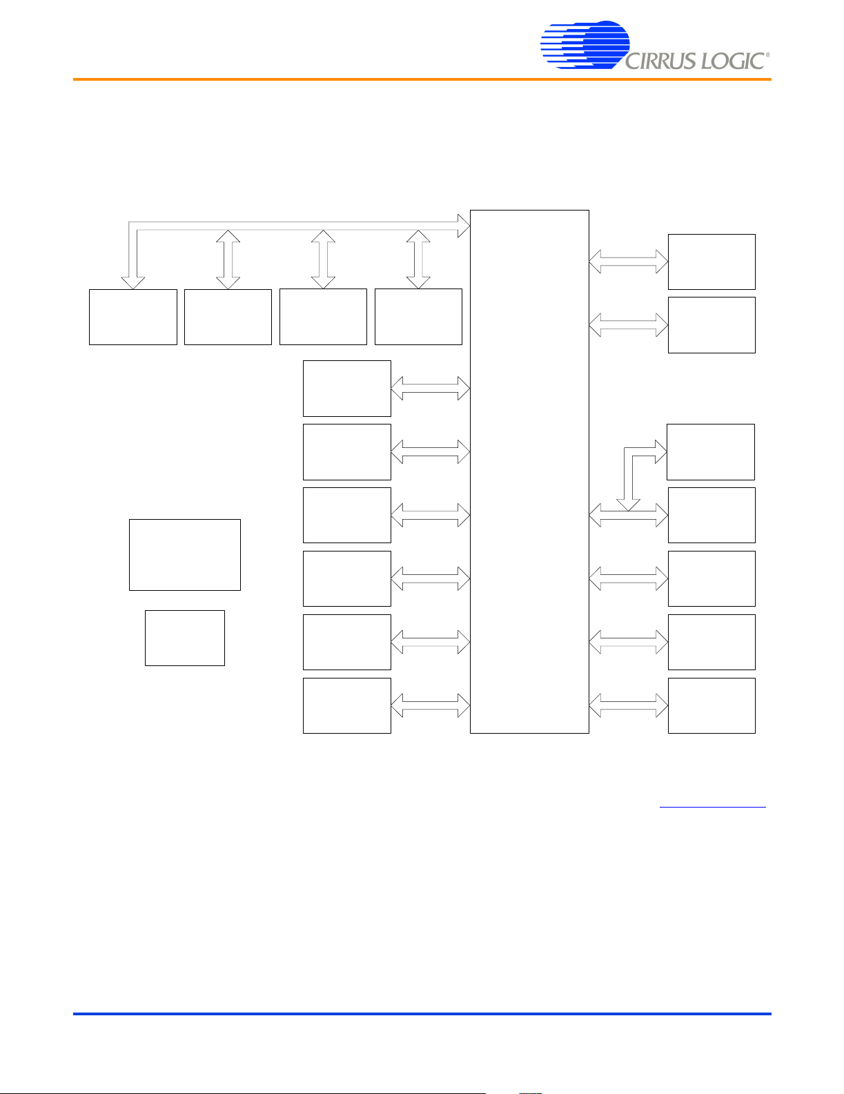
Figure 3. Block Diagram..........................................................................................................................10
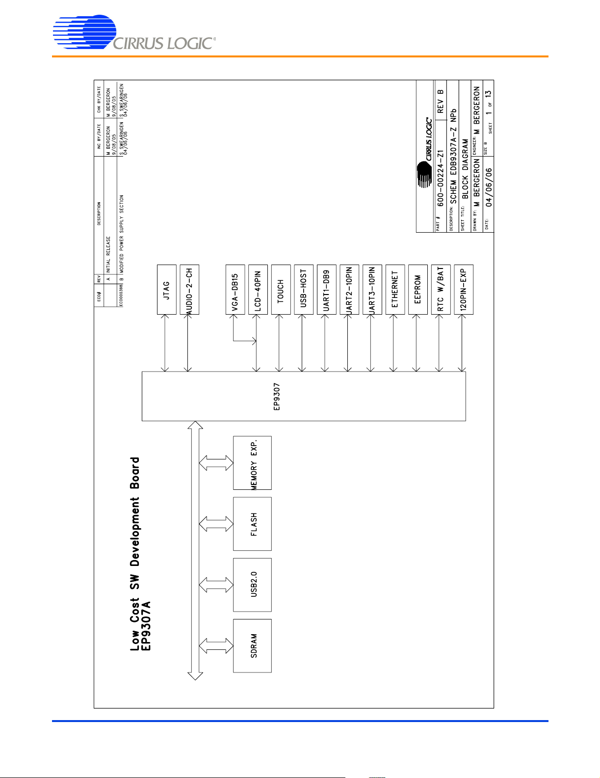
Figure 4. Schematic Page 1 - Block Diagram .........................................................................................19
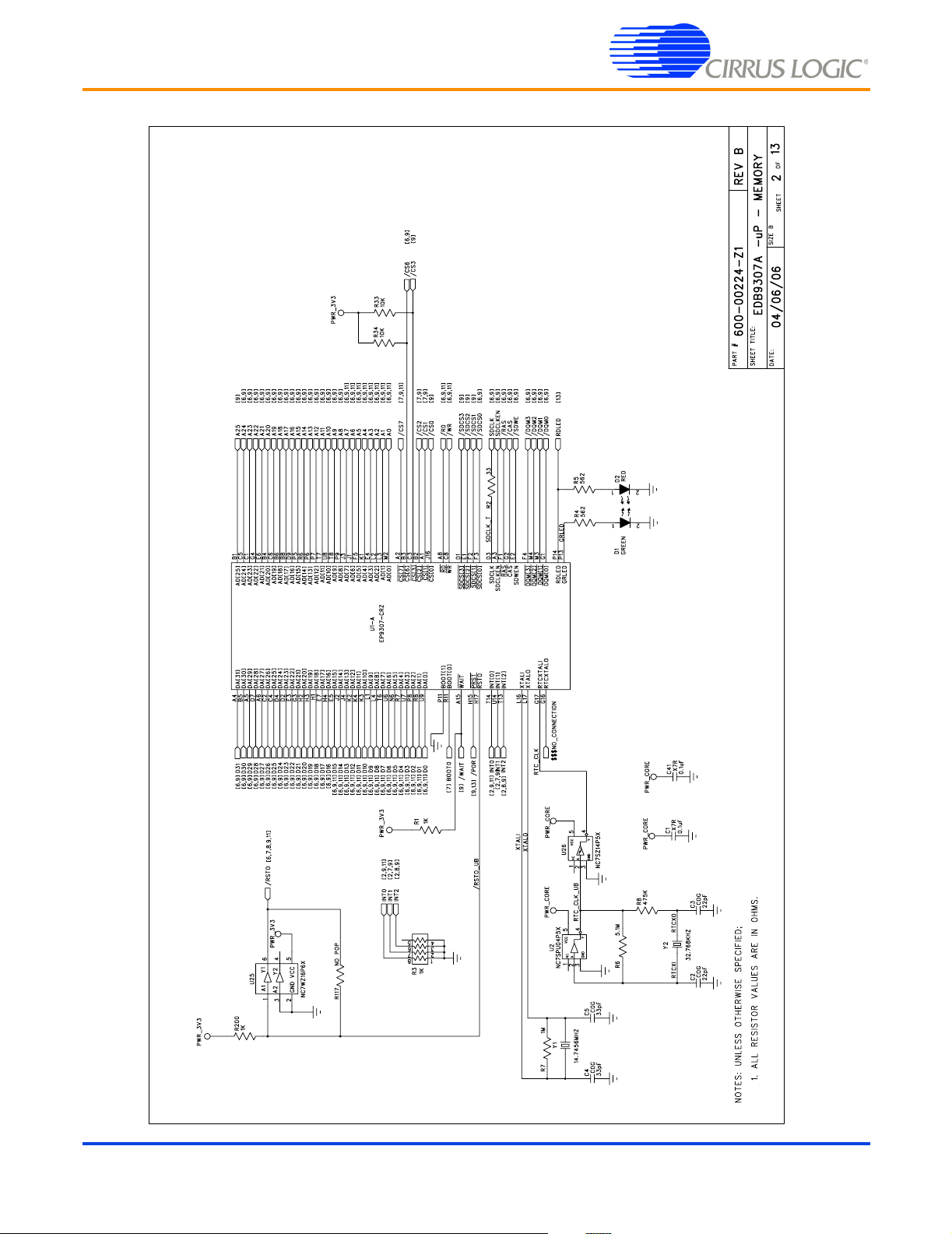
Figure 5. Schematic Page 2 - Processor & Memory ...............................................................................20
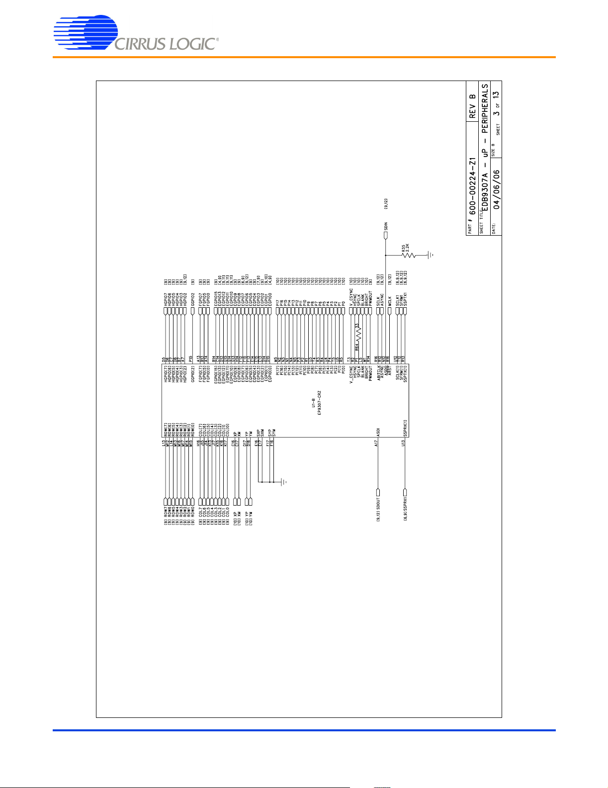
Figure 6. Schematic Page 3 - Peripherals ..............................................................................................21
Figure 7. Schematic Page 4 - UARTs & USB .........................................................................................22
Figure 8. Schematic Page 5 - mP Power................................................................................................23
Figure 9. Schematic Page 6 - SDRAM & Flash ......................................................................................24
Figure 10. Schematic Page 7 - JTAG & CFG .........................................................................................25
Figure 11. Schematic Page 8 - Ethernet.................................................................................................26
Figure 12. Schematic Page 9 - Expansion Connector ............................................................................27
Figure 13. Schematic Page 10 - VGA & LCD .........................................................................................28
Figure 14. Schematic Page 11 - USB2.0 Slave ......................................................................................29
Figure 15. Schematic Page 12 - Audio ...................................................................................................30
Figure 16. Schematic Page 13 - Power Supply ......................................................................................31
List of Figures
4 ©Copyright 2006 Cirrus Logic, Inc. DS667DB1
Page 5
EDB9307A
Technical Reference Manual
1. EDB9307A Kit Contents
Each EDB9307A kit comes with the following:
• EDB9307A Development Board
• Null Modem Serial Cable
• Power Supply: +12V, 5A, 110V/220V with AC Power Cord
• Quick Start Guide
• Registration Card
• (2) IDC10-to-DB9 Cables
•IAR™ Evaluation CD
• Quick Start Guide
• Board Registration Card
• Trial Software Download Information Card
All documentation, schematics, software, utilities, and related information is available from the download
section of the Cirrus Logic ARM Developer's web site, http://arm.cirrus.com
.
Figure 1. EDB9307A Board
DS667DB1 ©Copyright 2006 Cirrus Logic, Inc. 5
Page 6

EDB9307A
Technical Reference Manual
2. Introducing the EDB9307A Engineering Development Board
This document will describe the features and basic operation of the EDB9307A board developed by
Cirrus Logic. Detailed information regarding the operation and programming of the EP9307 device are
covered by the EP9307 datasheet and User's Guide on the Cirrus Logic web site.
The EDB9307A is a convenient and easy-to-operate evaluation platform. It has been designed to provide
the majority of the EP9307 functions on a small 6" x 4" base board. These features include:
• EP9307 Processor Running at 200MHz
• 64MByte SDRAM
• 16MByte NOR Flash Memory
• Two USB 2.0 Full-speed Host Ports
• USB 2.0 High-speed Device Interface
• Audio Out
• Audio In
• Three UARTs
• 10/100 Ethernet Interface
•VGA
•JTAG
• Consumer IR (CIR)
• Expansion Connectors
• LCD Interface with Touch Screen Support
Note: The EDB9307A kit does not include a LCD screen. The LCD interface is pin-compatible with
previous Cirrus Logic development boards.
Not all features of the EP9307 are on the base board. Two high-density connectors have been provided
to allow for daughter card expansion. The full memory bus is connected to one of the connectors and
any peripherals not on the development board are attached to the other connector. In addition, some
features such as Ethernet MII interface have been brought out to the peripheral connector as well.
2.1 Identifying What's on the Board
Figure 2 shows the top side of the EDB9307A. The accompanying legend identifies the main
components of the board.
6 ©Copyright 2006 Cirrus Logic, Inc. DS667DB1
Page 7
EDB9307A
Technical Reference Manual
L
M N
K
Y
J
I
H
E
D
C
FG
X
O P
A
B
W
Q R
S
T
U
V
Figure 2. EDB9307A Top View
A. EP9307 Processor
B. Processor Status LEDs - one Red and one
Green
C. USB 2.0 High-speed Device IC (ISP1581)
D. SDRAM - 2 16-bit devices
E. Memory Bus Expansion Connector
F. Main Power Switch, S2
G. 12V Power Connector
H. 3.3V Voltage Regulator - switching, 3A
I. Serial Boot Pushbutton - labeled "SERIAL
BOOT"
J. Reset Pushbutton - labeled "/POR"
K. UART2 Header - 5x2
M. UART0, DB9 Male
N. USB Device Connector
O. Ethernet Connector
P. Dual, Stacked USB Host Connector
Q. Audio Out Connector
R. Audio In Connector
S. Peripheral Bus Expansion Connector
T. Touch Screen Connector
U. JTAG Connector
V. VGA Connector - DB15, female
W. LCD Connector
X. Commercial IR
Y. RTC and Battery Backup
L. UART1 Header - 5x2
One item not listed above is the Flash device. It is located on the bottom side of the board, under item C.
There are no jumpers on the board. The only "jumper" is the serial boot pushbutton. This button is used
when the developer wants to use the Cirrus Logic download utility to put new code into Flash memory.
DS667DB1 ©Copyright 2006 Cirrus Logic, Inc. 7
Page 8
EDB9307A
Technical Reference Manual
3. Getting Started
3.1 Before you Begin...
The developer will find it useful to have some additional hardware not provided in the EDB9307A kit.
Items such as a USB mouse, USB keyboard, VGA monitor and cable, and a set of powered speakers
can make using the EDB9307A and the software installed on the board more enjoyable.
Caution: Make sure you are in a static-free environment and are following proper
procedures for handling ESD-sensitive electronic equipment.
3.2 Attaching Cables
Before attaching cables to the board make sure you know where pin 1 for each of the connectors is
located. Most connectors are keyed. However, some connectors use 2 x n headers, allowing the cable to
be plugged in backwards. Prime examples of this are the Touch Screen and JTAG connectors.
There is silkscreen on the PCB identifying each connector and its pin 1 location. Make sure to pay
attention to the markings on the PCB for the pin 1 location. The pin 1 identifier is marked by either a
number or a triangle.
3.3 Before Applying Power...
In order to use the EDB9307A the user must first connect the peripherals to the EDB9307A as described
in the following procedure.
1. Place the EDB9307A on a static free surface.
2. Make sure power switch S2 is in the OFF position.
3. Connect the 12V power supply provided to the board at J10.
4. Connect null modem serial cable provided in the kit from DB9 connector J2 to a serial port on a PC
or notebook (if so equipped).
5. Connect a VGA monitor to DB15 connector J6.
6. Launch a terminal program, such as minicom or HyperTerminal. Configure the PC com port for:
38400 baud, 8 data bits, no parity, 1 stop bit, no flow control for WinCE and 57600 baud for Linux.
7. Connect the board to a network that has internet access (optional)
8. Connect a USB mouse and keyboard.
9. Turn power switch S2 to the ON position and the board will boot and shortly display the WinCE 5.0 or
8 ©Copyright 2006 Cirrus Logic, Inc. DS667DB1
Page 9

EDB9307A
Technical Reference Manual
the Qt/Opie desktop on the VGA monitor, depending which OS you have programmed into the board.
The EDB9307A comes with WinCE 5.0 installed.
NOTE: The WinCE 5.0 binary is not provided on the support web site. If you erase the image on the
board, you will have to download the BSP provided by Cirrus Logic and compile it using Platform
Builder.
Due to changes in distribution policy, the Microsoft trial CD/DVD that was formerly included in
the kit is no longer available. Please refer to the card in the kit that describes how to download
the Microsoft trial software from the Microsoft web site.
DS667DB1 ©Copyright 2006 Cirrus Logic, Inc. 9
Page 10
EDB9307A
Technical Reference Manual
4. EDB9307A Circuit Description
This chapter makes reference to the schematics in Appendix A and discusses the main circuit
functionality of each schematic page. A detailed block diagram of the EDB9307A Engineering
Development Board is shown below.
JTAG
20 pin
Memory
Expansion
120 pin
Vout=1.8, 3.3, 5.0
POWER
Vin = +12V
Reset and
voltage
monitoring
SDRAM
64MByte
32-bit
USB 2.0
Device
(High Speed)
RTC
battery backed
CIR
UART1
UART2
10 pin
Ethernent
RJ45
Serial
EEPROM
Peripheral
Expansion
120 pin
Flash
16MByte
16-bit
Audio In
Audio Out
VGA
DB15
EP9307
LCD
40 pin
Touchscreen
10 pin
Dual USB 2.0
Host
(Full Speed)
UART0
DB9 w/control
Figure 3. Block Diagram
Detailed information regarding the EP9307 processor and interfaces can be found at www.cirrus.com.
The details of this device will not be discussed in this document. Refer to the EP9307 datasheet, User's
Guide, and other information on the web site for more information.
10 ©Copyright 2006 Cirrus Logic, Inc. DS667DB1
Page 11

EDB9307A
Technical Reference Manual
4.1 Circuit Operation
The major circuit operation for each page of the schematic will be discussed.
Note: Refer to http://arm.cirrus.com for the latest board schematics. Look under the download link at the top of the
page.
Page 1
Block diagram and revision history.
Page 2
There are two main clock inputs to the EP9307 device. One is the 14.7456 MHz crystal oscillator and the
other is the 32.768 kHz real time clock (RTC).
The 14.7456 MHz clock can be generated from a crystal circuit as shown in the schematics, or optionally
from a 14.7456 MHz oscillator. If a 14.7456 MHz oscillator is used, then only the XTALI pin is driven and
the drive level of the clock must be 3.3 V.
The RTC clock may be generated by the circuit shown in the schematics, or optionally an RTC oscillator.
Due to the cost of RTC oscillators, the circuit shown in the schematics is used. An external oscillator is
made by using an unbuffered '04 inverter. It is very important to use an unbuffered inverter in this
application. Using a buffered inverter may make the circuit oscillate in the ~MHz range or not start at all.
Refer to application note AN265.
The two LEDs connected to the EP9307 device are used to indicate processor health during boot and
general status of the board.
The reset output, RSTON (active-low signal) is buffered by U25. There is a resistor option for the RSTON
signal to be either driven by this buffer or bypassed. If the reset signal is not going to be buffered, U25
must be removed and R117 installed. By default, RSTON is buffered.
Page 3
This block shows the peripheral connections from the EP9307 processor.
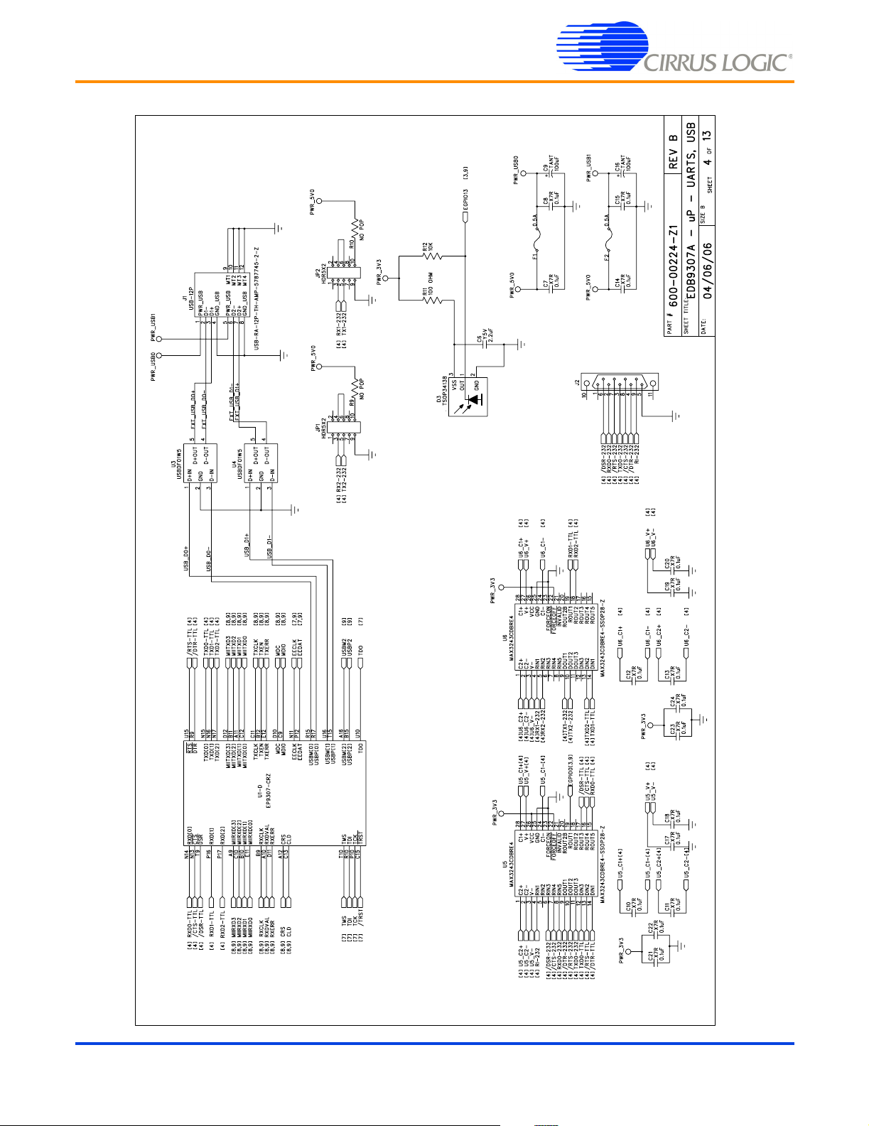
Page 4
Main items on this page are the USB 2.0 Full-speed Host, USB power, UART, and Commercial IR (CIR)
circuits.
The USB Host circuits are connected directly from the EP9307 to U3 and U4 and then on to the stacked
USB connector, J1. U3 and U4 provide termination for the USB signals and ESD protection. Note that
only two of the three USB ports are routed to USB connectors, the remaining USB port is routed to the
Peripheral Expansion header. Power for the USB Host ports comes from the +5V switching regulator and
is protected with poly fuses rated for 0.5 A each.
The board has all three UARTs brought out. The main UART interface, UART0, is connected to a
standard male DB9 connector and provides for full modem control. The other two UART interfaces are
connected to 5x2 headers. There is an option for installing zero-ohm resistors if the developer needs to
provide +5V power to an external device. The pinout of the headers matches common IDC10-to-DB9
cables. Two such cables are included with the kit. All UART signals are level shifted from TTL to RS-232.
The CIR uses an enhanced GPIO (EGPIO) line to communicate to the EP9307 device.
DS667DB1 ©Copyright 2006 Cirrus Logic, Inc. 11
Page 12

EDB9307A
Technical Reference Manual
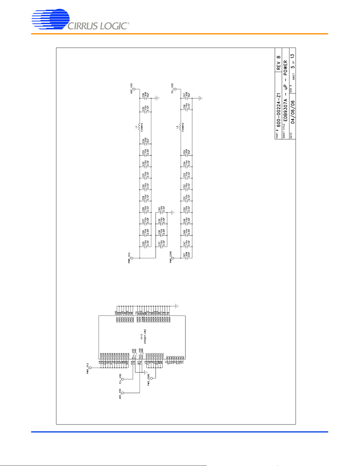
Page 5
This is the power section for the EP9307 device. The ADC and PLL supplies are filtered. There is no
reason to filter the 3.3 and the 1.8V power rails.
Page 6
The SDRAM interface is comprised of two 16-bit SDRAM devices to form a 32-bit SDRAM bus. The
SDRAM is connected to /SDCS0 and is located at physical memory address 0xC000_0000. Single 32bit SDRAM devices may be used as well.
The Flash interface is made from a single 16-bit device. It uses a "multi-cell" Flash device. The Flash
device is connected to /CS6 and is located at physical memory address 0x6000_0000. The reference
design uses only one Flash device. However, the EP9307 can be designed with a 32-bit Flash interface
as well. The Flash device installed is a 128 Mbit, 16 Mbyte, device.
The serial EEPROM is a 4 Mbit device and may be used for serial "SPI Boot" or for storing the Ethernet
MAC address. SPI Boot is not used as the default boot method but may be used by the developer if it fits
his/her application. Details about SPI Boot are in the EP9307 User's Guide. The serial EEPROM is
accessed only if the EGPIO7 line is configured to the proper level. The SPI™ frame signal and the
EGPIO7 "enable" signal are OR'ed to create the enable for the serial EEPROM device. EGPIO7 must be
low in order to communicate to the serial EEPROM. Other devices on the SPI bus must be enabled in a
similar manner but not enabled simultaneously.
Note: EGPIO7 should be pulled low instead of pulled high. If SPI Boot is desired, remove R201 and pull down
EGPIO7.
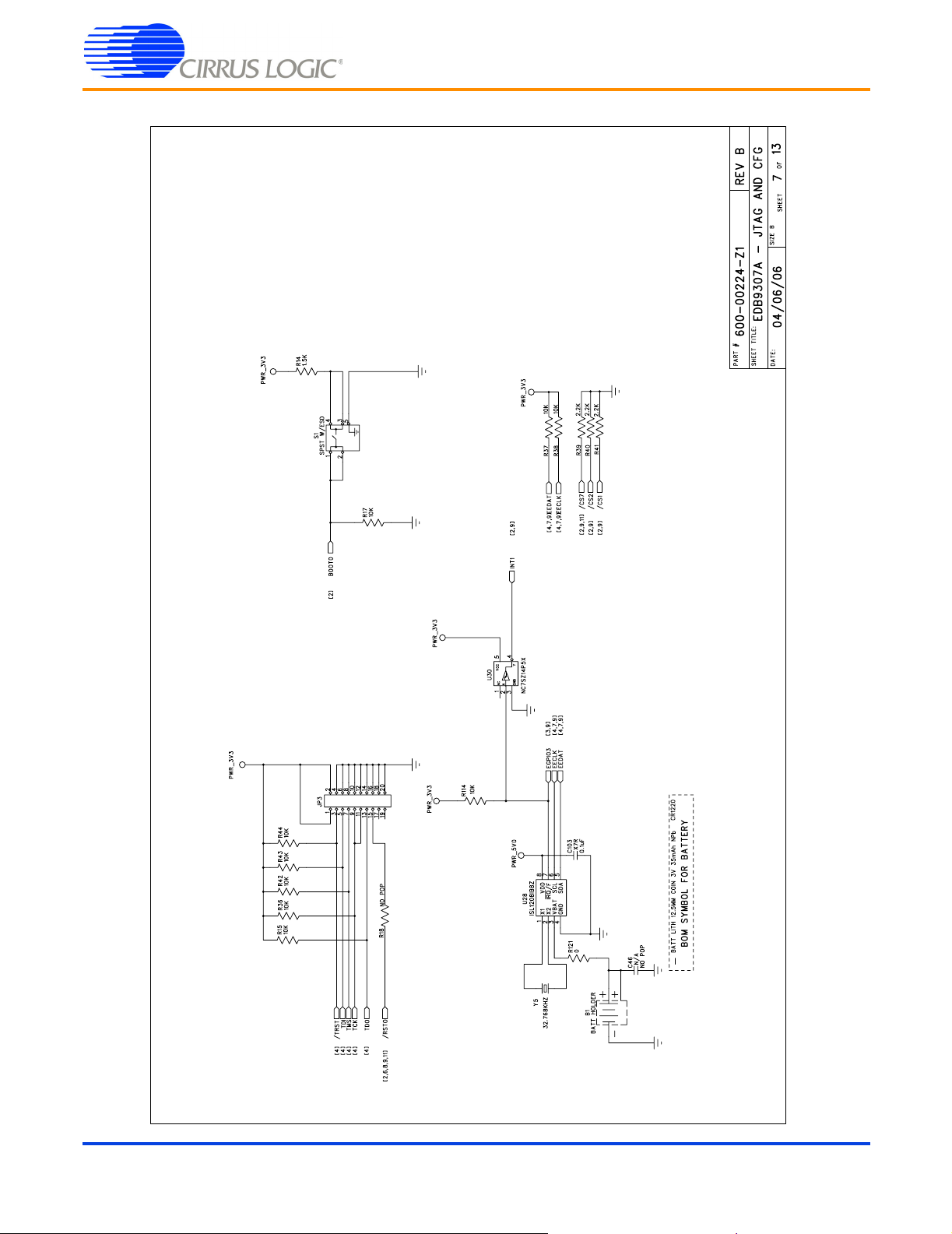
Page 7
The JTAG interface is connected to a 2x10 header, JP3. This connector is wired for the Multi-ICE
debugger.
There are 10 signals that determine how the EP9307 will boot and operate. They are all shown on this
page except for BOOT1. BOOT1 is connected to GND. BOOT1 is used for factory testing only. The other
nine signals are either pulled up or down external to the EP9307 device. The boot configuration shown
sets the EP9307 device to perform an Internal Async boot from a 16-bit-wide memory.
The “Serial Boot” pushbutton, S1, is used to configure the board to perform a serial boot. A serial boot is
used to program the Flash device with the Cirrus Logic download utility. Instead of using jumpers, a
pushbutton is used. Simply hold the pushbutton down while pressing and releasing the reset pushbutton,
S3. Continue to hold S1 until the red LED turns off. Once the red LED is off, release S1.
The ISL1208 is connected to the EP9307 to provided an external, battery backed RTC clock. This device
has 2 bytes of battery backed SRAM. The battery is a common lithium coin cell and easily removable if
desired.
Page 8
The Micrel KS8721Bl PHY is used to provide the 10/100 Mbit Ethernet interface. The PHY is attached to
the EP9307 device MII interface. The PHY also connects to RJ45 connector, J3. The Ethernet connector
has integrated magnetics and status LEDs. The Micrel PHY requires external power filtering of the 2.5V
supply it produces.
12 ©Copyright 2006 Cirrus Logic, Inc. DS667DB1
Page 13

EDB9307A
Technical Reference Manual
Page 9
The two connectors provide a daughter card interface for making custom circuits. J4 is the Memory
Expansion connector and J5 is the Peripheral Expansion connector.
The entire memory bus is connected to J5. It is recommended that the bus signals be buffered if adding
additional memory. However if a CPLD or FPGA is attached there is no reason to buffer. Use proper
engineering practices when using the high-speed memory bus with daughter cards.
The Peripheral Expansion bus has the signals for features not implemented on the EDB9307A board and
for commonly used signals.
Page 10
Two video interfaces are provided. The main video interface is VGA. An LCD interface is also provided
however there is no LCD screen included with the development kit. The LCD interface is pin compatible
with previous Cirrus Logic ARM9 development boards. A 4-wire touch screen interface is also included
and is pin compatible with previous Cirrus Logic ARM9 development boards.
Page 11
An external USB 2.0 High-speed Peripheral device is provided. The USB device allows a Host to see the
board as a Mass Storage device. The USB interface chip is connected to the lower 16-bits of the
memory bus.
Page 12
Audio is supported by a Cirrus Logic CS4271 device. Two-channel audio out and line-level audio in is
supported. The audio device communicates to the EP9307 through the I
are generated by the EP9307. The audio in is line level, it is not a microphone-level input. Like the serial
EEPROM, the CS4271 is controlled by the SPI frame signal and EGPIO6. EGPIO6 must be low in order
to communicate to the CS4271 device. As mentioned before, only one SPI™ device can be enabled at a
time.
2
S interface and audio clocks
DS667DB1 ©Copyright 2006 Cirrus Logic, Inc. 13
Page 14

EDB9307A
Technical Reference Manual
Page 13
Power and reset circuits are shown on this page. Most of the changes made to this revision of the
EDB9307A board were made in this section. The most important change made is that the board is now
powered from a +12V power supply instead of the former +5V supply.
The board has two connectors for input power. J10 is the standard power connector and is where the
power supply provided in the kit attaches. However, a 3x1 header, J11 is also available to supply power
to the board.
The 3.3V power rail is generated from a 3A, adjustable, switching regulator, U27. The 5V power rail is
generated from an identical 3A switching regulator, U28. The 5V supply requires a diode, D7. The 3.3V
supply does not require this diode.
The 1.8V power rail is generated from an 800mA linear regulator. Both the 3.3V and 1.8V power rails are
are monitored by U22 and it will issue a reset if either supply falls below the threshold voltage.
The reset pushbutton can connect directly to the voltage monitor reset input or to a supplementary resetdetect circuit. Refer to AN258 for more information. This circuit is implemented by U24 and some passive
devices. In general, this circuit is not required with EP9307 Rev E2 devices and may be removed if
desired. It is installed by default. If removed, R109 needs to be installed if the use of the reset pushbutton
is desired.
14 ©Copyright 2006 Cirrus Logic, Inc. DS667DB1
Page 15

EDB9307A
Technical Reference Manual
5. Software
5.1 Overview
The software programmed into the Flash on the EDB9307A development board is WinCE® 5.0. Linux
2.6.8.1, from Cirrus Logic, running Qt/Opie is also available for the EDB9307A board
The WinCE 5.0 image programmed into Flash by the factory is not available from Cirrus Logic directly.
This image can not be provided to users due to distribution and royalty reasons. If the developer decides
to overwrite the factory WinCE 5.0 Flash image with Linux or some other software, and then later desires
to put the WinCE 5.0 image back into Flash, they must obtain the WinCE 5.0 BSP from their Cirrus Logic
FAE and build the image themselves using the trial version of Platform Builder™ or with a version of
Platform Builder they have purchased. Only WinCE 5.0 supports the EDB9307A board. Cirrus Logic
technical support for WinCE 4.2 is not available.
Cirrus Logic provides complete source for its Linux 2.6 offering. The Cirrus Logic release images for the
EDB9307A are also provided for those who do not want to build the toolchain and environment or want a
quick way to load Linux onto the board. If, however, you wish to implement functionality other than that
provided in the release package images, you must download the gcc toolchain from the Cirrus Logic
User's Development Forum, under the download link at the top of the page
http://arm.cirrus.com/files/tools
location and let it download and build all the appropriate packages and toolchain.
. The other method is to download the buildroot package from the same
®
Note: Linux development should be done on a Linux PC, not under Windows. Cirrus Logic uses Debian as the
default build environment. Red Hat
2.6. development is done under Debian.
®
and other versions of Linux may be used as well, but Cirrus Logic Linux
5.2 Download Utility
The download utility provides the user with a tool for programming the flash memory on the EDB9307A
Development Board with a binary image. Two versions of the download executable are provided: one
supporting a PC running Windows/DOS, and one supporting a PC running Linux. The following
procedure will allow in-circuit programming of the flash memory via the EP9307 processor:
1. Connect null-modem serial cable to the DB9 connector on the board and to the PC.
2. Run the download utility; make sure all terminal windows are "Disconnected" Assuming the
download utility is located in same directory as the binary image…
a.For Windows: download binary_image_filename.bin
b.For Linux: download binary_image_filename.bin
3. "Waiting for board to wake up…" message is displayed on the PC.
4. Press and hold down pushbutton S1 "SERIAL BOOT"
5. Press and then release pushbutton S3 "/POR"
6. Wait for the red LED to go off then release pushbutton S1.
7. Messages will be displayed regarding erasing, then programming the flash.
8. "Successfully programmed binary_image_filename.bin" message displayed upon programming
completion.
9. Press pushbutton S3 to reboot the board with the new code image.
DS667DB1 ©Copyright 2006 Cirrus Logic, Inc. 15
Page 16

EDB9307A
Technical Reference Manual
6. Developer’s User Forum
Many references have been made to the Cirrus Logic Developers User's Forum in this document.
The Cirrus Logic Developers User's Forum is a company-sponsored site and moderated by Cirrus Logic
®
employees. However, it is not the technical help line for the Cirrus Logic ARM
product line. It is intended
to be a place where developers can share ideas and ask questions from others.
Developers should become familiar with the Developer's User Forum and the files provided under the
download link. Both software and hardware files are provided for Cirrus Logic offerings. Refer to
Chapter 7 for useful information related to the Cirrus Logic ARM products.
16 ©Copyright 2006 Cirrus Logic, Inc. DS667DB1
Page 17

7. Other Useful Information
Web Sites
• Cirrus Logic main web site: www.cirrus.com
• Developer's Web Site: arm.cirrus.com
• Registration Web Site: www.cirrus.com/boardreg
Processor Information
The following information is located on the www.cirrus.com web site.
• EP9307 Datasheet
• EP9307 User's Guide
• EP9307 Errata
Application Notes
The following information is located on the www.cirrus.com web site.
EDB9307A
Technical Reference Manual
• AN273, “EP93xx Silicon Rev E Design Guidelines”
• AN265, “EP93xx RTC Oscillator Circuit”
• AN258, “EP93xx Power-up and Reset Lockup Workaround”
Board Information
The following information is located on the arm.cirrus.com web site.
• EDB9307A Technical Reference Manual
•Schematics
•BOM
• Artwork and PCB stackup
Code Information
The following information is located on the arm.cirrus.com web site.
•Linux 2.6
• Board utilities
•Tools
Contact a Cirrus Logic FAE for information regarding the following.
• WinCE 5.0 BSP
The documents listed above are updated periodically and may be more up to date than the information in
this document. Check with the web sites for the latest updates.
DS667DB1 ©Copyright 2006 Cirrus Logic, Inc. 17
Page 18

EDB9307A
Technical Reference Manual
Appendix A. Schematics
The schematics for the EDB9307A Development Board are located on the Cirrus Logic Developer’s
Forum website ( arm.cirrus.com
(PDF) and PADS™ format. OrCAD™ versions of the schematics are not available.
). The schematics are provided in Adobe’s portable document format
18 ©Copyright 2006 Cirrus Logic, Inc. DS667DB1
Page 19
EDB9307A
Technical Reference Manual
Figure 4. Schematic Page 1 - Block Diagram
DS667DB1 ©Copyright 2006 Cirrus Logic, Inc. 19
Page 20
EDB9307A
Technical Reference Manual
Figure 5. Schematic Page 2 - Processor & Memory
20 ©Copyright 2006 Cirrus Logic, Inc. DS667DB1
Page 21
EDB9307A
Technical Reference Manual
Figure 6. Schematic Page 3 - Peripherals
DS667DB1 ©Copyright 2006 Cirrus Logic, Inc. 21
Page 22
EDB9307A
Technical Reference Manual
Figure 7. Schematic Page 4 - UARTs & USB
22 ©Copyright 2006 Cirrus Logic, Inc. DS667DB1
Page 23
EDB9307A
Technical Reference Manual
Figure 8. Schematic Page 5 - µP Power
DS667DB1 ©Copyright 2006 Cirrus Logic, Inc. 23
Page 24

EDB9307A
Technical Reference Manual
Figure 9. Schematic Page 6 - SDRAM & Flash
24 ©Copyright 2006 Cirrus Logic, Inc. DS667DB1
Page 25
EDB9307A
Technical Reference Manual
Figure 10. Schematic Page 7 - JTAG & CFG
DS667DB1 ©Copyright 2006 Cirrus Logic, Inc. 25
Page 26

EDB9307A
Technical Reference Manual
Figure 11. Schematic Page 8 - Ethernet
26 ©Copyright 2006 Cirrus Logic, Inc. DS667DB1
Page 27

EDB9307A
Technical Reference Manual
Figure 12. Schematic Page 9 - Expansion Connector
DS667DB1 ©Copyright 2006 Cirrus Logic, Inc. 27
Page 28

EDB9307A
Technical Reference Manual
Figure 13. Schematic Page 10 - VGA & LCD
28 ©Copyright 2006 Cirrus Logic, Inc. DS667DB1
Page 29

EDB9307A
Technical Reference Manual
Figure 14. Schematic Page 11 - USB2.0 Slave
DS667DB1 ©Copyright 2006 Cirrus Logic, Inc. 29
Page 30

EDB9307A
Technical Reference Manual
Figure 15. Schematic Page 12 - Audio
30 ©Copyright 2006 Cirrus Logic, Inc. DS667DB1
Page 31

EDB9307A
Technical Reference Manual
Figure 16. Schematic Page 13 - Power Supply
DS667DB1 ©Copyright 2006 Cirrus Logic, Inc. 31
Page 32

EDB9307A
Technical Reference Manual
Appendix B. Programming Linux Images into Flash from a Windows® PC
For those people who want to program Linux images onto the board but do not have a Linux PC.
Materials and Equipment Needed
A. +12V, 5 amp power supply, provided with kit
B. Computer
• Must be running Windows® 2000 or Windows® XP with SP2 installed on a Pentium® III or better
with at least 256M RAM.
• Must have at least one (1) serial port with DB9 connector.
• Must have at least one (1) Ethernet 10/100 port with RJ45 connector.
• Must have HyperTerminal software (comes with Windows 2000/XP).
• Must be able to connect to the Internet and download files from web site.
• Monitor, keyboard and mouse.
C. Cables
• One DB9 Null Model cable with female to female connectors, provided with kit
• One Ethernet cross-over cable, not provided with kit
D. Software
Linux images are provided by Cirrus Logic. The Linux files are on the http://arm.cirrus.com
website.
Click on the download link at the top of the page.
The files are in various directories and depend on the kernel version, build revision and board type you
need.
http://arm.cirrus.com/files/linux/releases/linux-2.6/1.0.4/edb9307A
has the image files:
redboot.bin, zImage and ramdisk.gz
Look for the version you are interested in and download the pre-built images.
Go to http://arm.cirrus.com/files/tools
to get the Windows download utility called, download.zip.
E. PC Software
• TFTP software
F. Hardware
• VGA monitor for the EDB9307A board
Note: The instructions and screen shots in this Appendix make reference to the SolarWinds 6.0 TFTP server program. This program
is not provided by Cirrus Logic. Other TFTP server programs may work equally well but will need to be verified by the developer.
32 ©Copyright 2006 Cirrus Logic, Inc. DS667DB1
Page 33
EDB9307A
Technical Reference Manual
Downloading Files
1. Make a directory called "TFTPROOT" on C:\
2. Use a computer that has an Internet connection and download the files specified in "D. Software"
to the directory made in step 1.
3. Disconnect the Ethernet cable if using Wired Ethernet. Plug in the Ethernet cross-over cable into
the computer's Ethernet port.
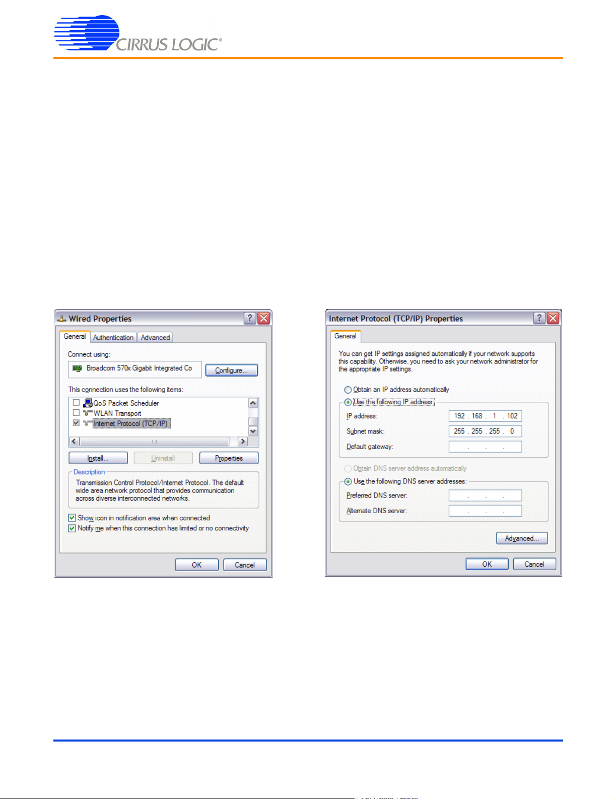
Windows PC Ethernet Setup
1. Go to Control Panel, click on Network Connections. Click on the Ethernet port icon representing
the RJ45 port on the computer. In the scroll box, go to the end and double click on the item called
Internet Protocol (TCP/IP).
2. Under the General tab, enable Use the following IP address and configure per the picture below.
When done, click on OK and then OK again for changes to take effect.
Note: The IP address can be any address you chose, just make sure it matches the IP address you use in the fconfig step below.
DS667DB1 ©Copyright 2006 Cirrus Logic, Inc. 33
Page 34
EDB9307A
Technical Reference Manual
TFTP Server Setup (Setup may vary depending on TFTP server used)
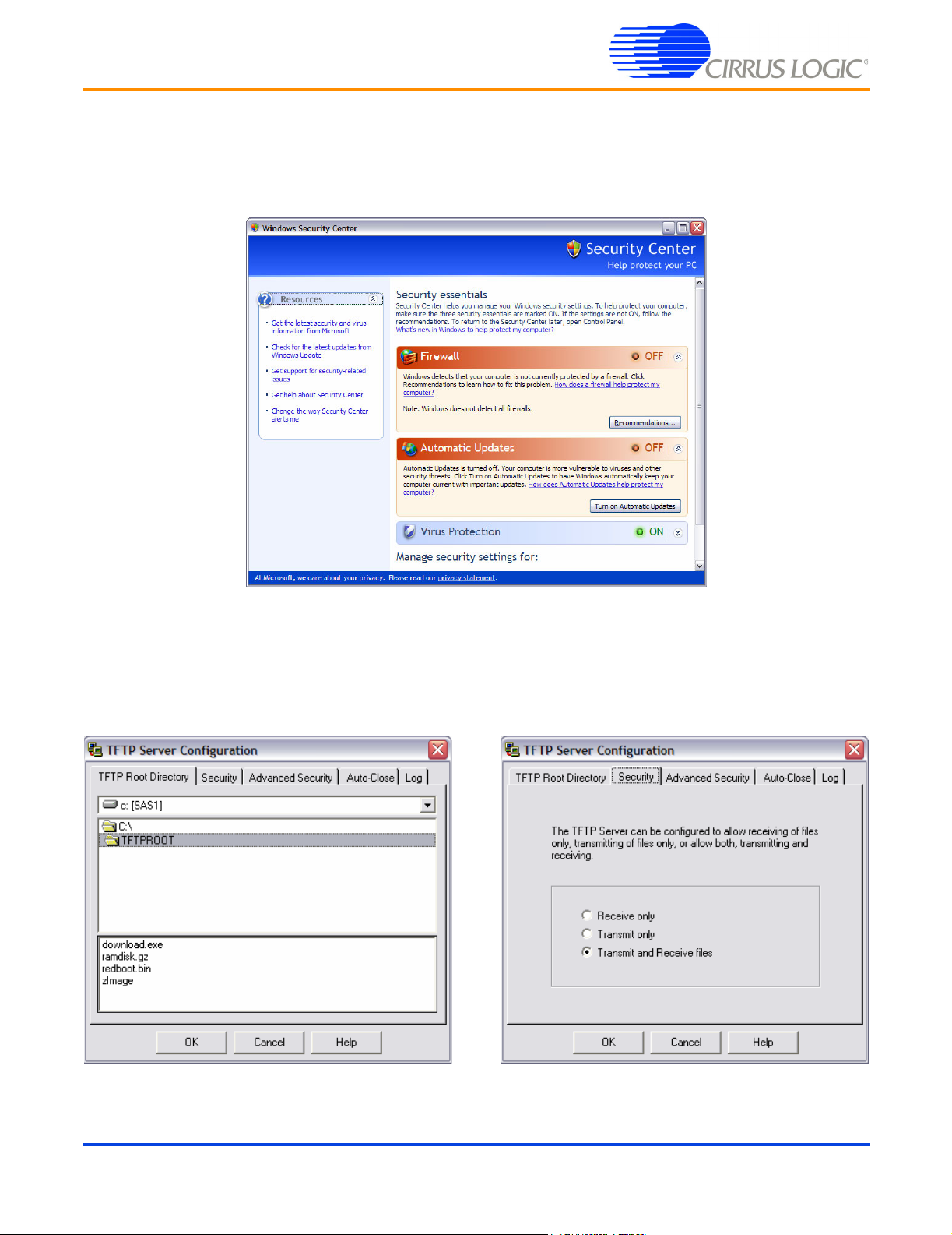
1. Install the TFTP Server program on the Windows PC and select the default configuration.
2. You may have to disable the firewall if using Windows XP.
3. Once the program is installed, run the TFTP Server program.
4. Configure the TFTP Root directory to point to C:\TFTPROOT.
5. Select the Security Tab and make sure the Client access is Transmit and Receive files. See the
pictures below.
34 ©Copyright 2006 Cirrus Logic, Inc. DS667DB1
Page 35
EDB9307A
Technical Reference Manual
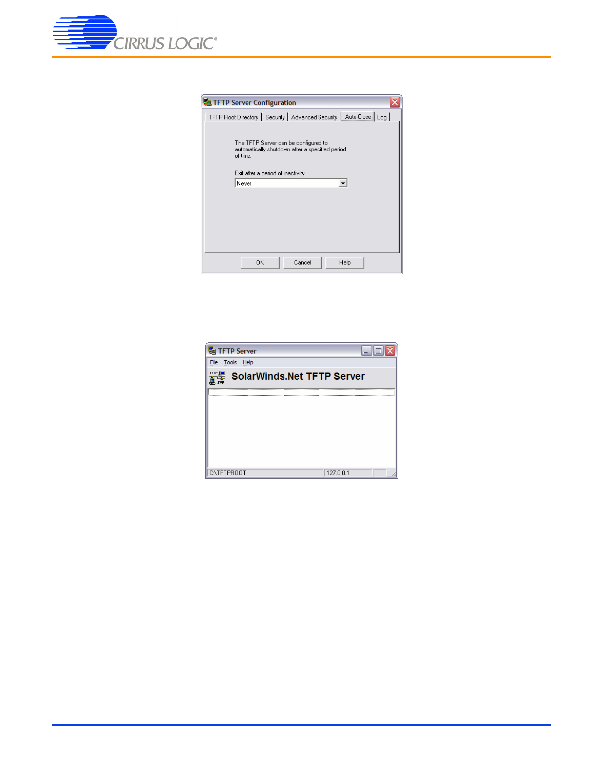
6. Verify that the Auto-Close setting is set to "Never".
7. When complete, click the OK button. You should see a screen like the picture below. Note that
the directory is located in the status bar at the bottom left. Additionally, the IP address the TFTP
Server is "listening" to is located in the lower right.
Note: Note: You may get an IP address of 127.0.0.1 because the EDB9307A board does not have the boot loader code
programmed yet. This is ok. Simply quit the TFTP server program. Instructions on when to start the program will be given
during the board programming section. If an IP address other then the one above appears, the Ethernet port is connected
to something and should be removed.
DS667DB1 ©Copyright 2006 Cirrus Logic, Inc. 35
Page 36
EDB9307A
Technical Reference Manual
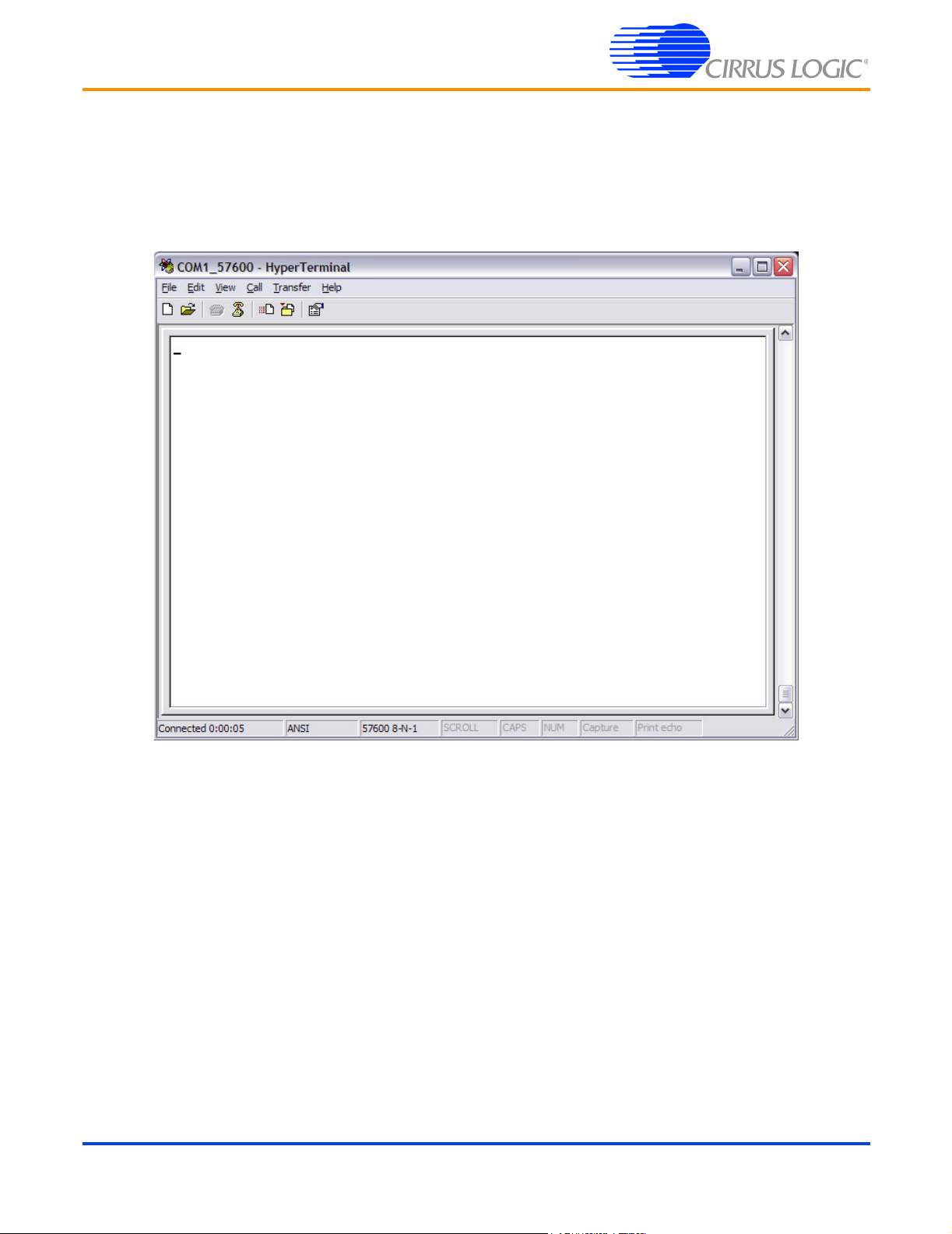
HyperTerminal Setup
Run the HyperTerminal program and configure to use COM1 and to run at 57600 baud, 8 data
bits, no parity, one (1) stop bit (8-N-1) and NO hardware control flow. It should look like the
picture below when complete. Note you have to "Disconnect" in order to make configuration
changes. Click "Call" once the configuration is complete.
36 ©Copyright 2006 Cirrus Logic, Inc. DS667DB1
Page 37
EDB9307A
Technical Reference Manual
Board Programming Setup
1. At this point, the RJ45 Ethernet port on the Windows PC is configured, HyperTerminal is running,
the TFTP server is running, the Cirrus Logic software has been downloaded to the
C:\TFTPROOT directory and the board is powered up.
2. Connect one end of the Null Modem cable to J2.
3. Connect the other end of the Null Modem cable to the COM1 port on the Windows 2000/XP
computer.
4. Connect the other end of the Ethernet cross-over cable to J3. A green LED in the J3 Ethernet
connector should light up.
5. Turn on the VGA monitor and plug the VGA monitor cable into DB15 connector J6.
6. Open a "Command Prompt" window so DOS commands can be issued.
7. Go to the C:\TFTPROOT directory by typing "cd\tftproot"
8. Click the "Disconnect" button in HyperTerminal to disable serial communication. HyperTerminal
has to be disconnected whenever the download.exe program is executed.
Programming Software into the Board
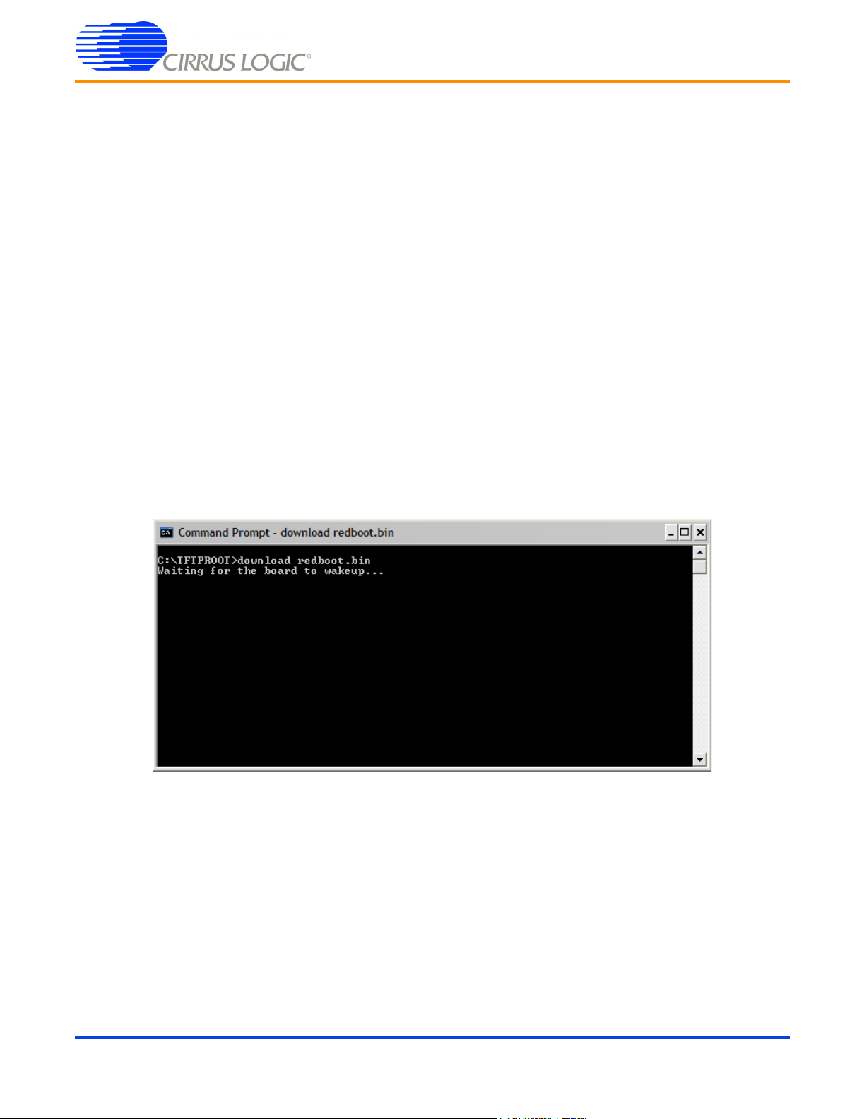
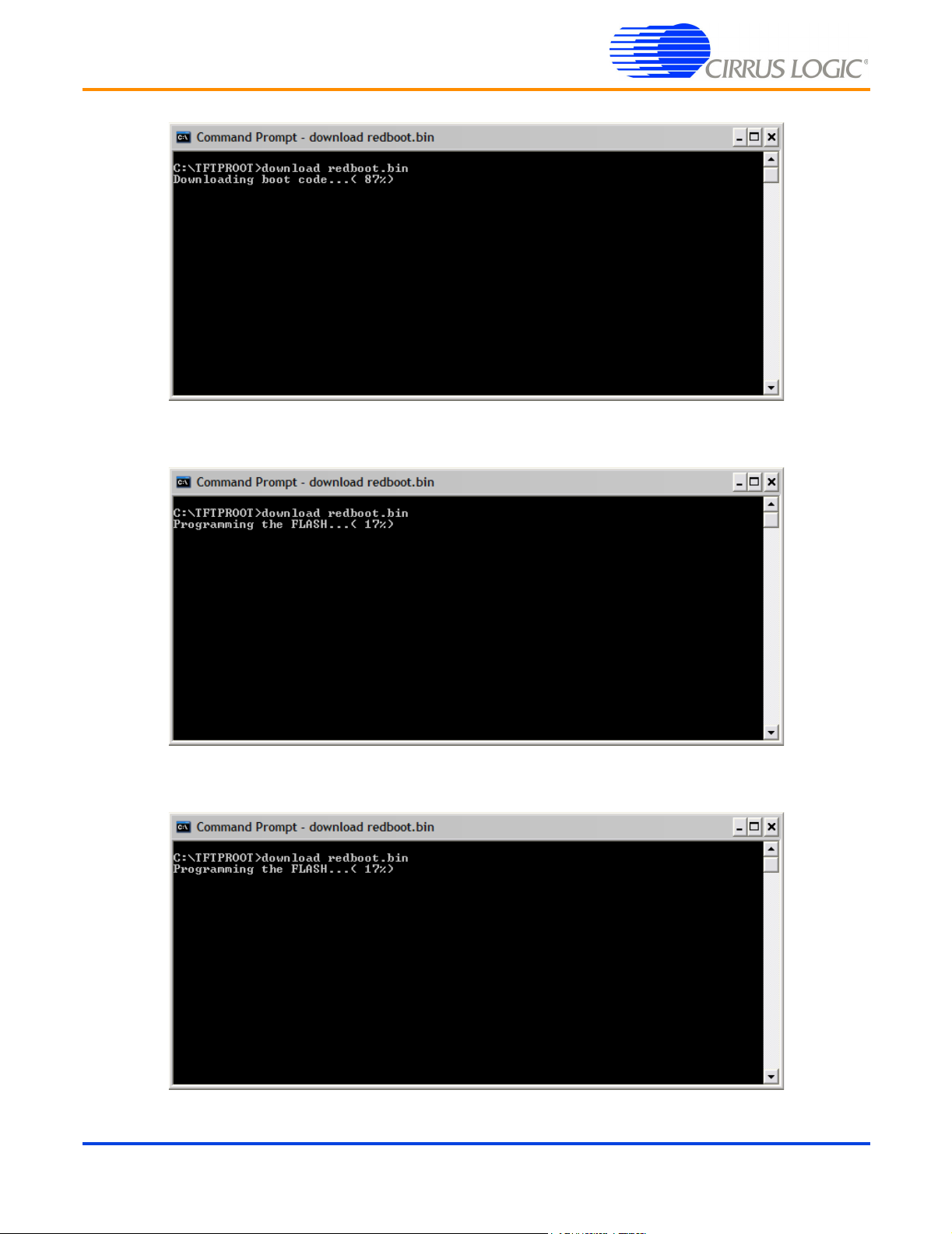
1. From the Command Prompt, type the following command: download redboot.bin.
2. At this point, the download program is waiting for the user to press AND hold down pushbutton
S1 SERIAL BOOT. While holding down S1, press and release pushbutton S3 /POR. Keep
holding down S1 until red LED, D2 (next to the flashing green LED) is no longer illuminated.
Afterwards, release S1. You should then see the following in the Command Prompt window.
DS667DB1 ©Copyright 2006 Cirrus Logic, Inc. 37
Page 38
EDB9307A
Technical Reference Manual
download.exe Downloading the Code
download.exe Erasing then Programming the Flash Memory
download.exe Successfully Programming redboot.bin
38 ©Copyright 2006 Cirrus Logic, Inc. DS667DB1
Page 39
EDB9307A
Technical Reference Manual
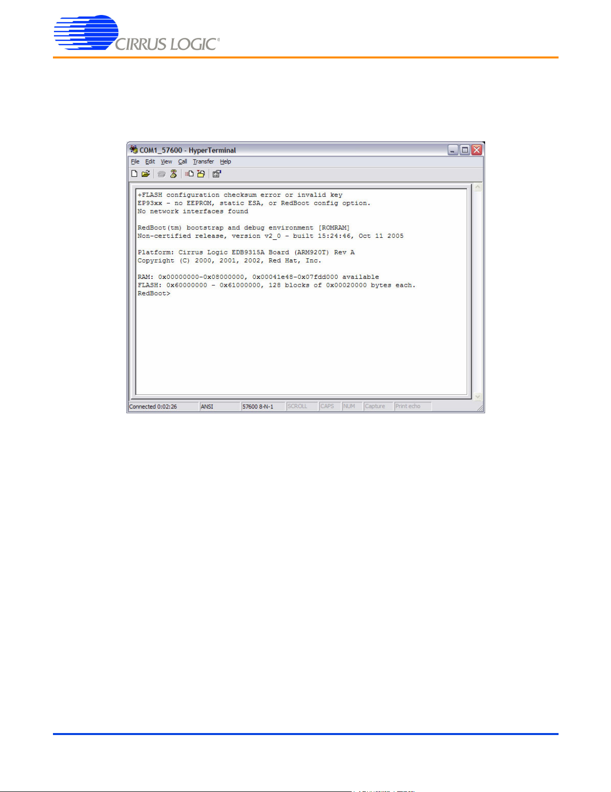
3. Redboot.bin has been programmed into Flash memory. Go to HyperTerminal and re-establish
serial communication to the board by pressing the Call button.
4. Press and release pushbutton S3, /POR. The board will reboot and eventually display
information in the HyperTerminal window.
Note: The initial error about configuration checksum error is expected for a brand new board or a board where the Flash device
has been completely erased. This happens because the Flash memory has not been initialized for redboot yet.
Note: Linux is case sensitive, pay close attention to the commands that follow.
Note: Steps 5-9 are for new boards only or when putting Linux on the board for the first time or for boards where the Flash device
has been completely erased. If you have already configured the board, proceed to step 10.
5. Initialize Flash memory by typing "fis init -f" at the RedBoot> prompt.
6. The next step is to configure the board so it can communicate via Ethernet. Type "fconfig" in the
HyperTerminal window and set all parameters like the picture below.
Note: You may have to hit the Backspace key to change some parameters and then type in the new parameter.
DS667DB1 ©Copyright 2006 Cirrus Logic, Inc. 39
Page 40
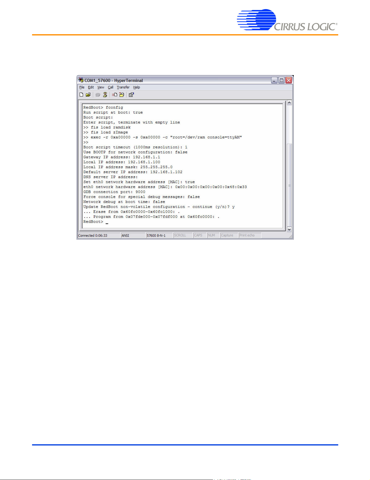
EDB9307A
Technical Reference Manual
7. The MAC address label on the top of the board has a hexadecimal number on it. It has the
following format: AB1234567890. When programming the MAC address, use the following
format: 0xAB:0x12:0x34:0x56:0x78:0x90. This is an example MAC address.
8. Remember, assign a unique MAC address to each board.
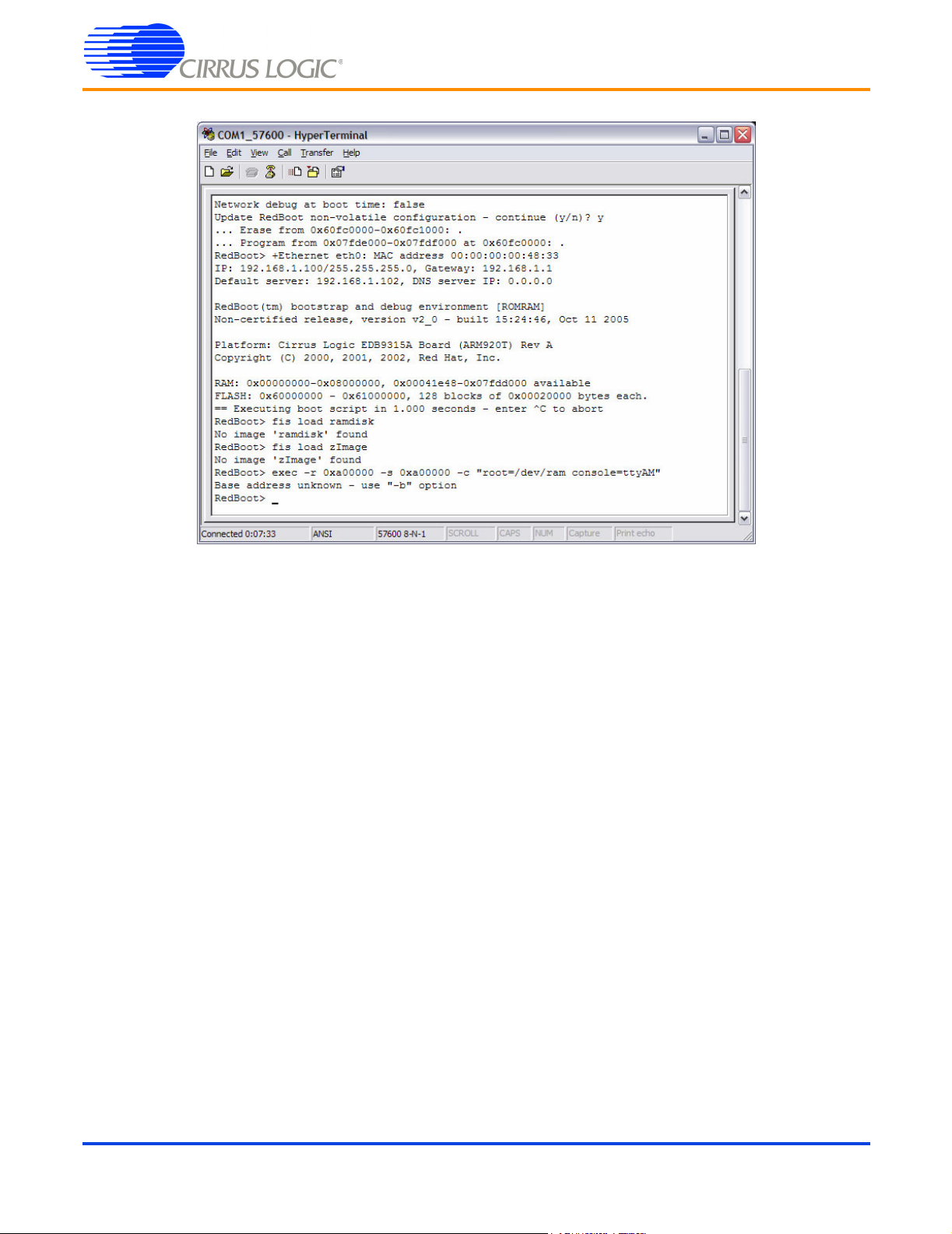
9. Press and release pushbutton S3 "/POR" for the changes to take effect. You should see the
following.
Note: It will say "No image 'image_name' found". That is ok for now. We have not downloaded and programmed those images into
Flash yet
40 ©Copyright 2006 Cirrus Logic, Inc. DS667DB1
Page 41
EDB9307A
Technical Reference Manual
10. Execute the following command: load -v -r -b 0xa00000 ramdisk.gz
11. You will see a spinning character in the bottom left hand side of the window. Wait until the
RedBoot> prompt returns.
12. Next type: fis create -b 0xa00000 -l 0xa00000 ramdisk
13. This command will program the ramdisk.gz file into a Flash partition called ramdisk. Wait until the
RedBoot> prompt returns.
14. Execute the following command: load -v -r -b 0x80000 zImage
15. You will see a spinning character in the bottom left hand side of the window. Wait until the
RedBoot> prompt returns.
16. Next type: fis create -b 0x80000 -l 0x140000 zImage
17. This command will program the zImage file into a Flash partition called zImage. Wait until the
RedBoot> prompt returns.
18. The software has now been programmed into Flash.
Note: The image sizes may increase as new features are added. In that case, some of the values in the load and fis create
commands may change. The size can be determined from the reported status after the load. Simply subtract the end
address from the start address. It is acceptable to make the partition larger than the exact image file size.
DS667DB1 ©Copyright 2006 Cirrus Logic, Inc. 41
Page 42

EDB9307A
Technical Reference Manual
Once the board has been programmed, reset the board and wait for it to boot up. You will see the
following (or similar) screen on the display..
42 ©Copyright 2006 Cirrus Logic, Inc. DS667DB1
Page 43

Revision History
Revision Date Changes
DB1 AUG 2006 First release.
EDB9307A
Technical Reference Manual
DS667DB1 ©Copyright 2006 Cirrus Logic, Inc. 43
Page 44

EDB9307A
Technical Reference Manual
Contacting Cirrus Logic Support
For all product questions and inquiries contact a Cirrus Logic Sales Representative.
To find the one nearest to you go to
IMPORTANT NOTICE
Cirrus Logic, Inc. and its subsidiaries ("Cirrus") believe that the information contained in this document is accurate and reliable. However, the information is subject to
change without notice and is provided "AS IS" without warranty of any kind (express or implied). Customers are advised to obtain the latest version of relevant information to verify, before placing orders, that information being relied on is current and complete. All products are sold subject to the terms and conditions of sale supplied
at the time of order acknowledgment, including those pertaining to warranty, indemnification, and limitation of liability. No responsibility is assumed by Cirrus for the
use of this information, including use of this information as the basis for manufacture or sale of any items, or for infringement of patents or other rights of third parties.
This document is the property of Cirrus and by furnishing this information, Cirrus grants no license, express or implied under any patents, mask work rights, copyrights,
trademarks, trade secrets or other intellectual property rights. Cirrus owns the copyrights associated with the information contained herein and gives consent for copies
to be made of the information only for use within your organization with respect to Cirrus integrated circuits or other products of Cirrus. This consent does not extend
to other copying such as copying for general distribution, advertising or promotional purposes, or for creating any work for resale.
CERTAIN APPLICATIONS USING SEMICONDUCTOR PRODUCTS MAY INVOLVE POTENTIAL RISKS OF DEATH, PERSONAL INJURY, OR SEVERE PROPERTY OR ENVIRONMENTAL DAMAGE ("CRITICAL APPLICATIONS"). CIRRUS PRODUCTS ARE NOT DESIGNED, AUTHORIZED OR WARRANTED FOR USE IN
AIRCRAFT SYSTEMS, MILITARY APPLICATIONS, PRODUCTS SURGICALLY IMPLANTED INTO THE BODY, AUTOMOTIVE SAFETY OR SECURITY DEVICES,
LIFE SUPPORT PRODUCTS OR OTHER CRITICAL APPLICATIONS. INCLUSION OF CIRRUS PRODUCTS IN SUCH APPLICATIONS IS UNDERSTOOD TO BE
FULLY AT THE CUSTOMER'S RISK AND CIRRUS DISCLAIMS AND MAKES NO WARRANTY, EXPRESS, STATUTORY OR IMPLIED, INCLUDING THE IMPLIED
WARRANTIES OF MERCHANTABILITY AND FITNESS FOR PARTICULAR PURPOSE, WITH REGARD TO ANY CIRRUS PRODUCT THAT IS USED IN SUCH A
MANNER. IF THE CUSTOMER OR CUSTOMER'S CUSTOMER USES OR PERMITS THE USE OF CIRRUS PRODUCTS IN CRITICAL APPLICATIONS, CUSTOMER AGREES, BY SUCH USE, TO FULLY INDEMNIFY CIRRUS, ITS OFFICERS, DIRECTORS, EMPLOYEES, DISTRIBUTORS AND OTHER AGENTS FROM
ANY AND ALL LIABILITY, INCLUDING ATTORNEYS' FEES AND COSTS, THAT MAY RESULT FROM OR ARISE IN CONNECTION WITH THESE USES.
Cirrus Logic, Cirrus, and the Cirrus Logic logo designs are trademarks of Cirrus Logic, Inc. All other brand and product names in this document may be trademarks
or service marks of their respective owners.
ARM, ARM9, RealView, and Multi-ICE
IAR is a trademark of IAR Syatem.
Windows, Windows XP, Windows 2000, and WinCE are registered trademarks of Microsoft Corporation.
Platform Builder is a trademark of Microsoft Corporation.
SPI is a trademark of Motorola, Inc..
Linux is a registered trademark of Linus Torvalds.
Red Hat is a registered trademark of Red Hat, Inc.
PADS is a trademark of Mentor Graphics Corporation.
OrCAD is a trademark of Cadence Design Systems, Inc.
Pentium is a registered trademark of Intel Corporation.
www.cirrus.com
are trademarks or registered trademarks of ARM Limited.
.
44 ©Copyright 2006 Cirrus Logic, Inc. DS667DB1
 Loading...