

Page 1
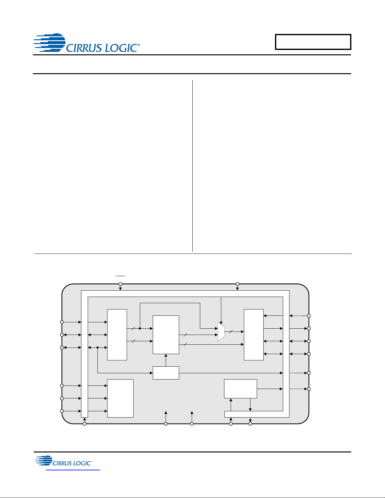
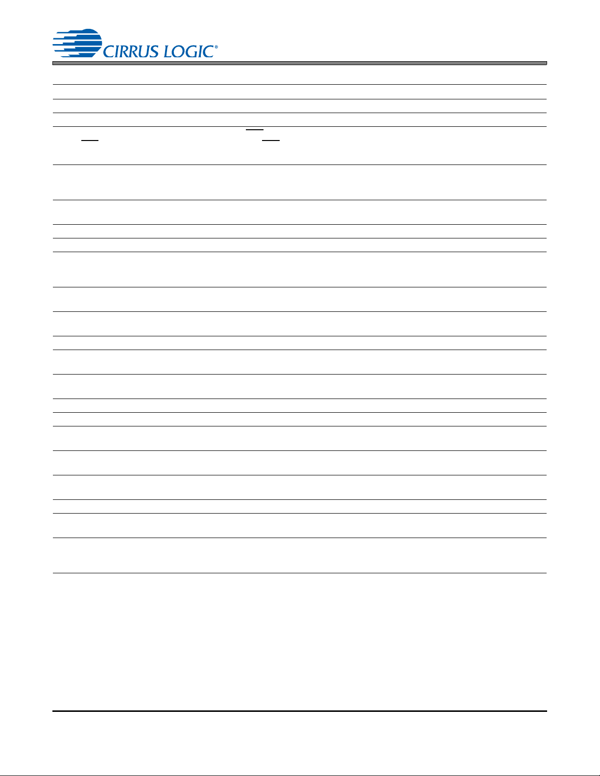
Serial
Audio
Input
Time
Varying
Digital
Filters
BYPASS
Digital
PLL
Clock
Generator
ILRCK
ISCLK
SDIN
Sync Info
Data
Serial
Audio
Output
OLRCK
OSCLK
SDOUT
XTI XTO
SRC_UNLOCK
2.5 V (VD) GND
RST
Sync Info
Data
Data
Level Translators
TDM_IN
MS_SEL
SAIF
SAOF
Serial
Port
Mode
Decoder
Level Translators
Level Translators
MCLK_OUT
3.3 V or 5.0 V (VL)
CS8421
32-bit, 192-kHz Asynchronous Sample Rate Converter
Features
175 dB Dynamic Range
–140 dB THD+N
No Programming Required
No External Master Clock Required
Supports Sample Rates up to 211 kHz
Input/Output Sample Rate Ratios of 7.5:1 to 1:8
Master Clock Support for 128 x Fs, 256 x Fs,
384 x Fs, and 512 x Fs (Master Mode)
16-, 20-, 24-, or 32-bit Data I/O
32-bit Internal Signal Processing
Dither Automatically Applied and Scaled to
Output Resolution
Flexible 3-wire Serial Digital Audio Input and
Output Ports
Master and Slave Modes for Both Input and
Output
Bypass Mode
Time Division Multiplexing (TDM) Mode
Attenuates Clock Jitter
Multiple Device Outputs are Phase Matched
Linear Phase FIR Filter
Automatic Soft Mute/Unmute
+2.5 V Digital Supply (VD)
+3.3 V or 5.0 V Digital Interface (VL)
Space-saving 20-pin TSSOP and QFN
Packages
The CS8421 supports sample rates up to 211 kHz and
is available in 20-pin TSSOP and QFN packages in both
Commercial (-10° to +70°C) and Automotive (-40° to
+85°C and -40° to +105°C) grades. The CDB8421 Customer Demonstration board is also available for device
evaluation and implementation suggestions. See “Or-
dering Information” on page 35 for complete details.
http://www.cirrus.com
Copyright Cirrus Logic, Inc. 2012
(All Rights Reserved)
JULY ‘12
DS641F6
Page 2

CS8421
General Description
The CS8421 is a 32-bit, high-performance, monolithic CMOS stereo asynchronous sample-rate converter.
Digital audio inputs and outputs can be 32, 24, 20, or 16 bits. Input and output data can be completely asynchronous,
synchronous to an external dat a clock, or the part can operate without any external clock by using an integrated
oscillator.
Audio data is input and output through configur able 3-wire input/output ports. The CS8421 does no t require any software control via a control port.
Target applications include digital recording systems (DVD-R/RW, CD-R/RW, PVR, DAT, MD, and VTR), digital mixing consoles, high-quality D/A, effects processors, computer audio systems, and automotive audio systems.
The CS8421 is also suitable for use as an asynchronous decimation or interpolation filter. See Cirrus Logic Application Note AN270, “Audio A/D Conversion with an Asynchronous Decimation Filter”, available at www.cirrus.com
for more details.
2 DS641F6
Page 3

TABLE OF CONTENTS
1. PIN DESCRIPTIONS ............................................................................................................................ 5
1.1 TSSOP Pin Descriptions ........... ... ... ... ... .... ... ... ... .... ... .......................................... ... ........................ 5
1.2 QFN Pin Descriptions .......................................................................... ... ... ... .... ... ... ... ... .................. 7
2. CHARACTERISTICS AND SPECIFICATIONS ..................................................................................... 9
SPECIFIED OPERATING CONDITIONS.............................................................................................. 9
ABSOLUTE MAXIMUM RATINGS........................................................................................................9
PERFORMANCE SPECIFICATIONS......................................... ......................................................... 10
DIGITAL FILTER CHARACTERISTICS .............................................................................................. 11
DC ELECTRICAL CHARACTERISTICS ....................... ... ... ... .... ... ... ... ... .......................................... ... 11
DIGITAL INPUT CHARACTERISTICS................................................................................................ 12
DIGITAL INTERFACE SPECIFICATIONS .......................................................................................... 12
SWITCHING SPECIFICATIONS ......................................................................................................... 12
3. TYPICAL CONNECTION DIAGRAMS ................................................................................................14
4. APPLICATIONS .................................................................................................................................. 16
4.1 Three-wire Serial Input/Output Audio Port .................................................................................... 16
4.2 Mode Selection .......................................................... ... .......................................... ... ................... 17
4.3 Sample Rate Converter (SRC) ..................................................................................................... 19
4.3.1 Data Resolution and Dither .............................. ... .... ... ... ... ... .... ... ... ... ................................ 19
4.3.2 SRC Locking and Varispeed .. ... .... ... .......................................... ... ... .... ... ... ... ... .... ... ... ... ... 19
4.3.3 Bypass Mode ......... ... .... ... ... ... ... .... ... ... ... .......................................... .... ............................ 19
4.3.4 Muting ....... ... .... ... ... ... .... ...................................... .... ... ... ... ... .... ......................................... 20
4.3.5 Group Delay and Phase Matching Between Multiple CS8421 Parts ............................... 20
4.3.6 Master Clock ....................................... ............................................................................. 20
4.3.7 Clocking .... ... .... ... ... ....................................... ... ... .... ... ... ... ................................................ 21
4.4 Time Division Multiplexing (TDM) Mode ....................................................................................... 21
4.5 Reset, Power-Down, and Start-Up ............................................................................................... 22
4.6 Power Supply, Grounding, and PCB Layout ................................................................................ 23
5. PERFORMANCE PLOTS ................................................................................................................ 24
6. PACKAGE DIMENSIONS ................................................................................................................... 33
TSSOP THERMAL CHARACTERISTICS ........................................... ... .... ... ... ... .... ............................ 33
QFN THERMAL CHARACTERISTICS.......................................... ... ... ... .... ... ... ... .... ... ... ... ... .... ... ... ... ... 34
7. ORDERING INFORMATION ............................................................................................................... 35
8. REVISION HISTORY .......................................................................................................................... 35
CS8421CS8421
LIST OF FIGURES
Figure 1. Non-TDM Slave Mode Timing..................................................................................................... 13
Figure 2. TDM Slave Mode Timing ............................................................................................................ 13
Figure 3. Non-TDM Master Mode Timing................................................................................................... 13
Figure 4. TDM Master Mode Timing .......................................................................................................... 13
Figure 5. Typical Connection Diagram, No External Master Clock............................ .... ............................ 14
Figure 6. Typical Connection Diagram, Master and Slave Modes............................................................. 15
Figure 7. Serial Audio Interface Format - I²S ............................................................................................. 17
Figure 8. Serial Audio Interface Format - Left-Justified.............................................................................. 17
Figure 9. Serial Audio Interface Format - Right-Justified ........................................................................... 17
Figure 10. Typical Connection Diagram for Crystal Circuit ........................................................................ 21
Figure 11. TDM Slave Mode Timing Diagram............................................................................................ 21
Figure 12. TDM Master Mode Timing Diagram.......................................................................................... 22
Figure 13. TDM Mode Configuration (All CS8421 Outputs are Slave)....................................................... 22
Figure 14. TDM Mode Configuration (First CS8421 Output is Master, All Others are Slave).................... 22
Figure 15. Wideband FFT Plot (16k Points) 0 dBFS 1 kHz Tone, 48 kHz:48 kHz..................................... 24
Figure 16. Wideband FFT Plot (16k Points) 0 dBFS 1 kHz Tone, 44.1 kHz:192 kHz................................ 24
Figure 17. Wideband FFT Plot (16k Points) 0 dBFS 1 kHz Tone, 44.1 kHz:48 kHz.................................. 24
DS641F6 3
Page 4

CS8421
Figure 18. Wideband FFT Plot (16k Points) 0 dBFS 1 kHz Tone, 48 kHz:44.1 kHz.................. .... ... ... ... ... 24
Figure 19. Wideband FFT Plot (16k Points) 0 dBFS 1 kHz Tone, 48 kHz:96 kHz.................. ... .... ... ... ... ... 24
Figure 20. Wideband FFT Plot (16k Points) 0 dBFS 1 kHz Tone, 96 kHz:48 kHz.................. ... .... ... ... ... ... 24
Figure 21. Wideband FFT Plot (16k Points) 0 dBFS 1 kHz Tone, 192 kHz:48 kHz................... .... ... ... ... ... 25
Figure 22. Wideband FFT Plot (16k Points) -60 dBFS 1 kHz Tone, 48 kHz: 96 kHz......... ... ... ... .... ... ... ... ... 25
Figure 23. Wideband FFT Plot (16k Points) -60 dBFS 1 kHz Tone, 48 kHz: 48 kHz......... ... ... ... .... ... ... ... ... 25
Figure 24. Wideband FFT Plot (16k Points) -60 dBFS 1 kHz Tone, 44.1 kHz:192 kHz. ... ... ... ... .... ... ... ... ... 25
Figure 25. Wideband FFT Plot (16k Points) -60 dBFS 1 kHz Tone, 44.1 kHz:48 kHz............................... 25
Figure 26. Wideband FFT Plot (16k Points) -60 dBFS 1 kHz Tone, 48 kHz: 44.1 kHz......... ... ... .... ... ... ... ... 25
Figure 27. Wideband FFT Plot (16k Points) -60 dBFS 1 kHz Tone, 96 kHz: 48 kHz......... ... ... ... .... ... ... ... ... 26
Figure 28. IMD, 10 kHz and 11 kHz -7 dBFS, 96 kHz:48 kHz ................................................................... 26
Figure 29. Wideband FFT Plot (16k Points) -60 dBFS 1 kHz Tone, 192 k Hz:48 kHz....... ... ... ... .... ... ... ... ... 26
Figure 30. IMD, 10 kHz and 11 kHz -7 dBFS, 48 kHz:44.1 kHz ................................................................ 26
Figure 31. IMD, 10 kHz and 11 kHz -7 dBFS, 44.1 kHz:48 kHz ................................................................ 26
Figure 32. Wideband FFT Plot (16k Points) 0 dBFS 20 kHz Tone, 44.1 kHz:48 kHz................................ 26
Figure 33. Wideband FFT Plot (16k Points) 0 dBFS 80 kHz Tone, 192 kHz:192 kHz............................... 27
Figure 34. Wideband FFT Plot (16k Points) 0 dBFS 20 kHz Tone, 48 kHz:96 kHz................ ... .... ... ... ... ... 27
Figure 35. Wideband FFT Plot (16k Points) 0 dBFS 20 kHz Tone, 48 kHz:48 kHz................ ... .... ... ... ... ... 27
Figure 36. Wideband FFT Plot (16k Points) 0 dBFS 20 kHz Tone, 96 kHz:48 kHz................ ... .... ... ... ... ... 27
Figure 37. Wideband FFT Plot (16k Points) 0 dBFS 20 kHz Tone, 48 kHz:44.1 kHz................ .... ... ... ... ... 27
Figure 38. THD+N vs. Output Sample Rate, 0 dBFS 1 kHz Tone, Fsi = 192 kHz ..................................... 27
Figure 39. THD+N vs. Output Sample Rate, 0 dBFS 1 kHz Tone, Fsi = 48 kHz ....................................... 28
Figure 40. THD+N vs. Output Sample Rate, 0 dBFS 1 kHz Tone, Fsi = 96 kHz ....................................... 28
Figure 41. THD+N vs. Output Sample Rate, 0 dBFS 1 kHz Tone, Fsi = 44.1 kHz .................................... 28
Figure 42. Dynamic Range vs. Output Sample Rate, -60 dBFS 1 kHz Tone, Fsi = 192 kHz . ... .... ...... ... ... 28
Figure 43. THD+N vs. Output Sample Rate, 0 dBFS 1 kHz Tone, Fsi = 32 kHz ....................................... 28
Figure 44. Dynamic Range vs. Output Sample Rate, -60 dBFS 1 kHz Tone, Fsi = 32 kHz ... ....... ... ... ... ... 28
Figure 45. Dynamic Range vs. Output Sample Rate, -60 dBFS 1 kHz Tone, Fsi = 96 kHz ... ....... ... ... ... ... 29
Figure 46. Dynamic Range vs. Output Sample Rate, -60 dBFS 1 kHz Tone, Fsi = 44.1 kHz ................... 29
Figure 47. Frequency Response with 0 dBFS Input ..................................................................................29
Figure 48. Passband Ripple, 192 kHz:48 kHz ..................... ... ... ... .... ... ... ... ... .... ... ... ................................... 29
Figure 49. Dynamic Range vs. Output Sample Rate, -60 dBFS 1 kHz Tone, Fsi = 48 kHz ... ....... ... ... ... ... 29
Figure 50. Linearity Error, 0 to -140 dBFS Input, 200 Hz Tone, 48 kHz:48 kHz........................................ 29
Figure 51. Linearity Error, 0 to -140 dBFS Input, 200 Hz Tone, 48 kHz:44.1 kHz..................................... 30
Figure 52. Linearity Error, 0 to -140 dBFS Input, 200 Hz Tone, 48 kHz:96 kHz........................................ 30
Figure 53. Linearity Error, 0 to -140 dBFS Input, 200 Hz Tone, 96 kHz:48 kHz........................................ 30
Figure 54. Linearity Error, 0 to -140 dBFS Input, 200 Hz Tone, 44.1 kHz:192 kHz................................... 30
Figure 55. Linearity Error, 0 to -140 dBFS Input, 200 Hz Tone, 44.1 kHz:48 kHz ..................................... 30
Figure 56. Linearity Error, 0 to -140 dBFS Input, 200 Hz Tone, 192 kHz:44.1 kHz................................... 30
Figure 57. THD+N vs. Input Amplitude, 1 kHz Tone, 48 kHz:44.1 kHz ..................................................... 31
Figure 58. THD+N vs. Input Amplitude, 1 kHz Tone, 48 kHz:96 kHz ........................................................ 31
Figure 59. THD+N vs. Input Amplitude, 1 kHz Tone, 96 kHz:48 kHz ........................................................ 31
Figure 60. THD+N vs. Input Amplitude, 1 kHz Tone, 44.1 kHz:192 kHz ................................................... 31
Figure 61. THD+N vs. Input Amplitude, 1 kHz Tone, 44.1 kHz:48 kHz ..................................................... 31
Figure 62. THD+N vs. Input Amplitude, 1 kHz Tone, 192 kHz:48 kHz ...................................................... 31
Figure 63. THD+N vs. Frequency Input, 0 dBFS, 48 kHz:44.1 kHz........................................................... 32
Figure 64. THD+N vs. Frequency Input, 0 dBFS, 48 kHz:96 kHz.............................................................. 32
Figure 65. THD+N vs. Frequency Input, 0 dBFS, 44.1 kHz:48 kHz........................................................... 32
Figure 66. THD+N vs. Frequency Input, 0 dBFS, 96 kHz:48 kHz.............................................................. 32
LIST OF TABLES
Table 1. Serial Audio Port Master/Slave and Clock Ratio Select Start-Up Options (MS_SEL) ................. 18
Table 2. Serial Audio Input Port Start-Up Options (SAIF).......................................................................... 18
Table 3. Serial Audio Output Port Start-Up Options (SAOF) ..................................................................... 18
4 DS641F6
Page 5
1. PIN DESCRIPTIONS
1
2
3
4
5
16
6
7
8
15
14
13
12
11
9
10
17
18
19
20
SRC_UNLOCK
XTO
SAIF
XTI
SAOF
VD
VL
GND
GND
RST
MS_SEL
BYPASS
OLRCK
ILRCK
OSCLK
ISCLK
SDOUT
SDIN
TDM_IN
MCLK_OUT
1.1 TSSOP PIN DESCRIPTIONS
CS8421CS8421
DS641F6 5
Page 6
Pin Name # Pin Description
XTO 1 Crystal Out (Output) - Crystal output for Master clock. See “Master Clock” on page 20.
XTI 2
VD 3 Digital Power (Input) - Digital core power supply. Typically +2.5 V.
GND 4 Ground (Input) - Ground for I/O and core logic.
RST
BYPASS 6
ILRCK 7
ISCLK 8 Serial Audio Bit Clock (Input/Output) - Serial-bit clock for audio data on the SDIN pin.
SDIN 9 Serial Audio Input Data Port (Input) - Audio data serial input pin.
MCLK_OUT 10
TDM_IN 11
SDOUT 12
OSCLK 13 Serial Audio Bit Clock (Input/Output) - Serial-bit clock for audio data on the SDOUT pin.
OLRCK 14
MS_SEL 15
GND 16 Ground (Input) - Ground for I/O and core logic.
VL 17 Logic Power (Input) - Input/Output power supply. Typically +3.3 V or +5.0 V.
SAOF 18
SAIF 19
SRC_UNLOCK 20
Crystal/Oscillator In (Input) - Crystal or digital clock input for Master clock. See “Master Clock”
on page 20.
Reset (Input) - When RST is low, the CS8421 enters a low-power mode and all internal states are
5
reset. On initial power-up, RST must be held low until the power supply is stable and all input
clocks are stable in frequency and phase.
Sample Rate Converter Bypass (Input) - When BYPASS is high, the sample rate converter will
be bypassed, and any data input through the serial audio input port will be directly output on the
serial audio output port. When BYPASS is low, the sample rate converter will operate normally.
Serial Audio Input Left/Right Clock (Input/Output) - Word-rate clock for the audio data on the
SDIN pin.
Master Clock Output (Output) - Buffered and level-shifted output for Master clock. If MCLK_OUT
is not required, this pin should be pulled high through a 47 k resistor to turn the output off. See
“Master Clock” on page 20.
Serial Audio TDM Input (Input) - Time Division Multiplexing serial audio data input. Grounded
when not used. See “Time Division Multiplexing (TDM) Mode” on page 21.
Serial Audio Output Data Port (Output) - Audio data serial output pin. Optionally , this pin may be
pulled low through a 47-k resistor, but must not be pulled high.
Serial Audio Input Left/Right Clock (Input/Output) - Word-rate clock for the audio data on the
SDOUT pin.
Master/Slave Select (Input) - Used to select Master or Slave for the input and output serial audio
ports at startup and reset. See Table 1 on page 18 for settings.
Serial Audio Output Format Select (Input) - Used to select the serial audio output format at
startup and reset. See Table 3 on page 18 for format settings.
Serial Audio Input Format Select (
and reset. See Table 2 on page 18 for format settings.
SRC Unlock Indicator (Output) - Indicates when the SRC is unlocked. See “SRC Locking and
Varispeed” on page 19.
Input) - Used to select the serial audio input format at startup
CS8421
6 DS641F6
Page 7
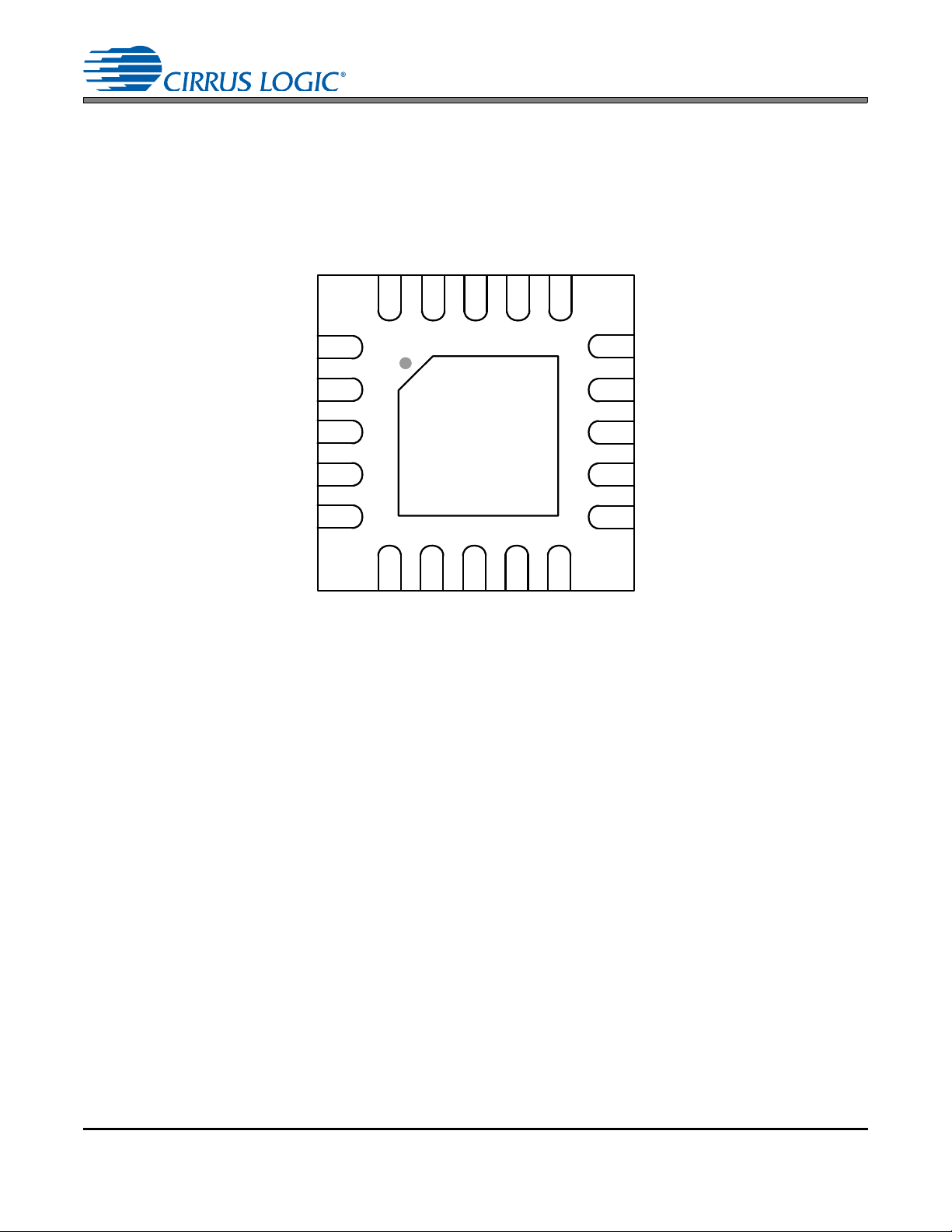
1.2 QFN PIN DESCRIPTIONS
76
5
4
3
2
1
8
9
10
11
12
13
14
15
16
17
181920
Top-Down View
20-pin QFN Package
Thermal Pad
XTI
XTO
SRC_UNLOC
SAIF
SAOF
ISCLK
SDIN
MCLK_OUT
TDM_IN
SDOUT
VD
GND
RST
BYPASS
ILRCK
VL
GND
MS_SEL
OLRCK
OSCLK
CS8421CS8421
DS641F6 7
Page 8
Pin Name # Pin Description
VD 1 Digital Power (Input) - Digital core power supply. Typically +2.5 V.
GND 2 Ground (Input) - Ground for I/O and core logic.
Reset (Input) - When RST
RST
BYPASS 4
ILRCK 5
ISCLK 6 Serial Audio Bit Clock (Input/Output) - Serial-bit clock for audio data on the SDIN pin.
SDIN 7 Se ria l Audi o In put Data Port (Input) - Audio data serial input pin.
MCLK_OUT 8
TDM_IN 9
SDOUT 10
OSCLK 11 Serial Audio Bit Clock (Input/Output) - Serial bit clock for audio data on the SDOUT pin.
OLRCK 12
MS_SEL 13
GND 14 Ground (Input) - Ground for I/O and core logic.
VL 15 Logic Power (Input) - Input/Output power supply. Typically +3.3 V or +5.0 V.
SAOF 16
SAIF 17
SRC_UNLOCK 18
XTO 19 Crystal Out (Output) - Crystal output for Master clock. See “Master Clock” on page 20.
XTI 20
Thermal Pad -
3
reset. On initial power-up, RST
are stable in frequency and phase.
Sample Rate Converter Bypass (Input) - When BYP ASS is high, the sample-rate converter will be
bypassed, and any data input through the serial audio input port will be directly output on the serial
audio output port. When BYPASS is low, the sample rate converter will operate normally.
Serial Audio Input Left/Right Cl oc k (Input/Output) - Word-rate clock for the audio data on the
SDIN pin.
Master Clock Output (Output) - Buffered and level-shifted output for Master clock. If MCLK_OUT
is not required, this pin should be pulled high through a 47 k resistor to turn the output off. See
“Master Clock” on page 20.
Serial Audio TDM Input (Input) - Time Division Multiplexing serial audio data input. Grounded
when not used. See “Time Division Multiplexing (TDM) Mode” on page 21.
Serial Audio Output Data Port (Output) - Audio data serial output pin. Optionally , this pin may be
pulled low through a 47-k resistor, but must not be pulled high.
Serial Audio Input Left/Right Cl oc k (Input/Output) - Word rate clock for the audio data on the
SDOUT pin.
Master/Slave Select (Input) - Used to select Master or Slave for the input and output serial audio
ports at startup and reset. See Table 1 on page 18 for settings.
Serial Audio Output Format Select (Input) - Used to select the serial audio output format at
startup and reset. See Table 3 on page 18 for format settings.
Serial Audio Input Format Select (Input) - Used to select the serial audio input format at startup
and reset. See Table 2 on page 18 for format settings.
SRC Unlock Indicator (Output) - Indicates when the SRC is unlocked. See “SRC Locking and
Varispeed” on page 19.
Crystal/Oscillator In (Input) - Crystal or digital clock input for Master clock. See “Master Clock” on
page 20.
Thermal Pad - Thermal relief pad for optimized heat dissipation. This pad must be electrically
connected to GND. See “Power Supply, Grounding, and PCB Layout” on page 23 for more
information.
is low, the CS8421 enters a low-power mode and all internal states are
must be held low until the power supply is stable and all input clocks
CS8421
8 DS641F6
Page 9
CS8421CS8421
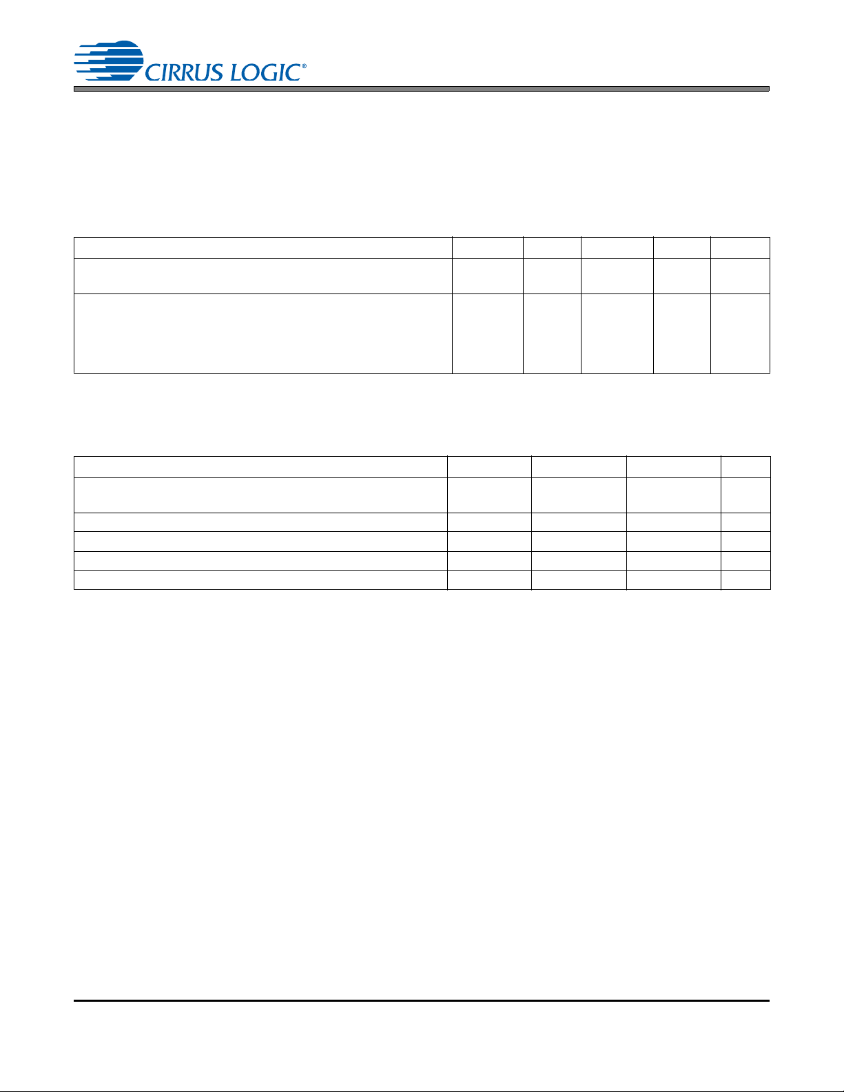
2. CHARACTERISTICS AND SPECIFICATIONS
(All Min/Max characteristics and specifications are guaranteed over the Specified Operating Conditions. Typical performance characteristics and specifications are derived from measurements taken at nominal supply voltages and
T
= 25°C.)
A
SPECIFIED OPERATING CONDITIONS
(GND = 0 V, all voltages with respect to 0 V)
Parameter Symbol Min Nominal Max Units
Power Supply Voltage VD
VL
Ambient Operating Temperature: ‘-CZ’
‘-CNZ’
‘-DZ’
‘-EZ’
‘-ENZ’
T
A
2.38
3.14
-10
-10
-40
-40
-40
2.5
3.3 or 5.0
-
-
-
-
-
2.62
5.25
+70
+70
+85
+105
+105
V
V
°C
°C
°C
°C
°C
ABSOLUTE MAXIMUM RATINGS
(GND = 0 V; all voltages with respect to 0 V. Operation beyond these limits may result in permanent damage to the device. Normal operation is not guaranteed at these extremes.)
Parameter Symbol Min Max Units
Power Supply Voltage VD
VL
Input Current, Any Pin Except Supplies (Note 1) I
Input Voltage V
Ambient Operating Temperature (power applied) T
Storage Temperature T
stg
in
in
A
-0.3
-0.3
-±10mA
-0.3 VL+0.4 V
-55 +125 °C
-65 +150 °C
3.5
6.0
V
V
Notes:
1. Transient currents of up to 100 mA will not cause SCR latch-up.
2. Numbers separated by a colon indicate input and output sample rates. For example, 48 kHz:96 kHz indicates that
Fsi = 48 khz and Fso = 96 kHz.
DS641F6 9
Page 10
CS8421
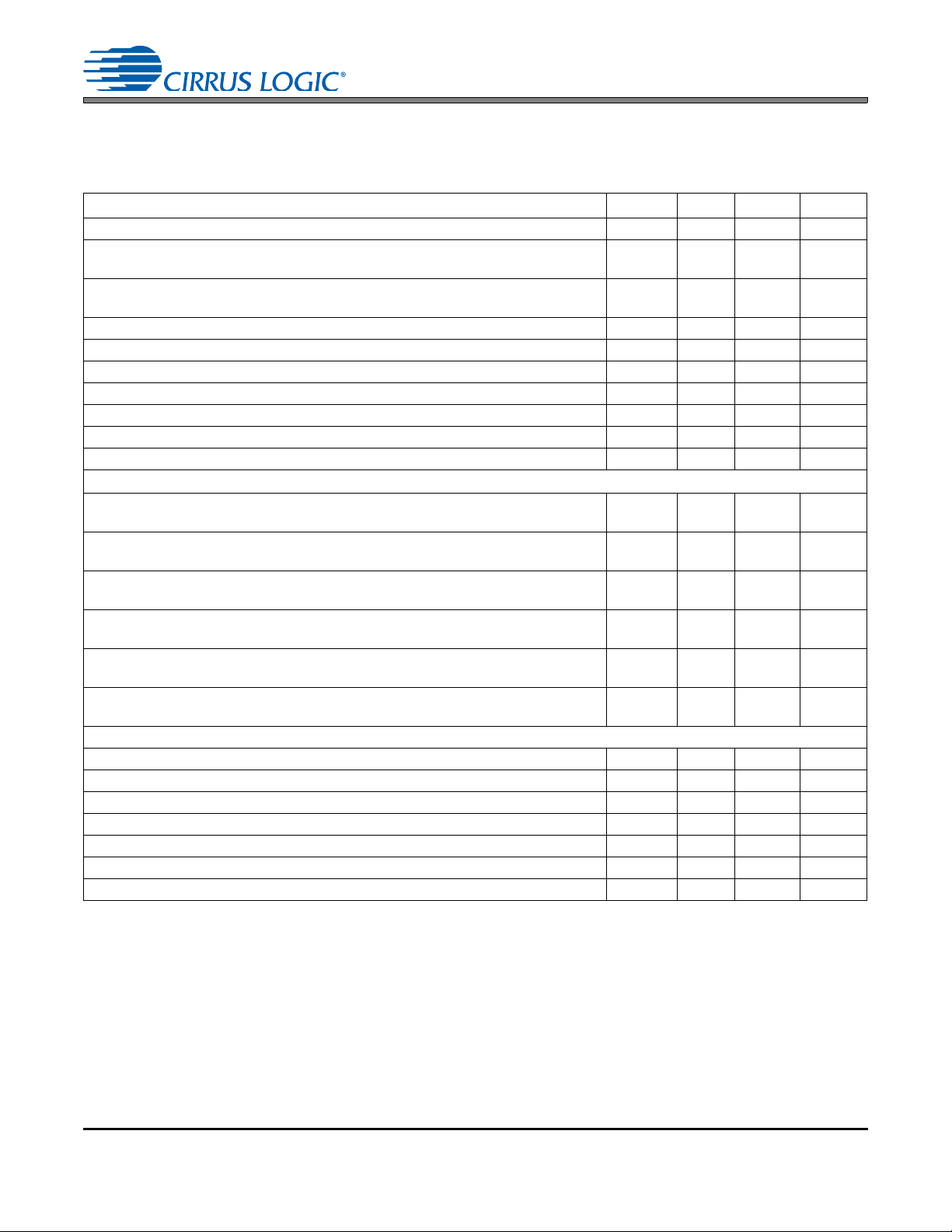
PERFORMANCE SPECIFICATIONS
(XTI/XTO = 27 MHz; Input signal = 1.000 kHz, 0 dBFS, Measurement Bandwidth = 20 to Fso/2 Hz, and Word Width = 32-Bits,
unless otherwise stated.)
Parameter Min Typ Max Units
Resolution 16 - 32 bits
Sample Rate with XTI = 27.000 MHz Slave
Master
Sample Rate with other XTI clocks Slave
Master
Sample Rate with ring oscillator (XTI to GND or VL, XTO floating) 12 - 96 kHz
Sample Rate Ratio - Upsampling - - 1:8
Sample Rate Ratio - Downsampling - - 7.5:1
Gain Error -0.2 - -0.02 dB
Interchannel Gain Mismatch - 0.0 - dB
Interchannel Phase Deviation - 0.0 - Degrees
Peak Idle Channel Noise Component (32-bit operation) - - -192 d B FS
Dynamic Range (20 Hz to Fso/2, 1 kHz, -60 dBFS Input)
44.1 kHz:48 kHz A-Weighted
Unweighted
44.1 kHz:192 kHz A-Weighted
Unweighted
48 kHz:44.1 kHz A-Weighted
Unweighted
48 kHz:96 kHz A-Weighted
Unweighted
96 kHz:48 kHz A-Weighted
Unweighted
192 kHz:32 kHz A-Weighted
Unweighted
Total Harmonic Distortion + Noise (20 Hz to Fso/2, 1 kHz, 0 dBFS Input)
32 kHz:48 kHz - -161 - dB
44.1 kHz:48 kHz - -171 - dB
44.1 kHz:192 kHz - -130 - dB
48 kHz:44.1 kHz - -160 - dB
48 kHz:96 kHz - -148 - dB
96 kHz:48 kHz - -168 - dB
192 kHz:32 kHz - -173 - dB
7.2
53
XTI/3750
XTI/512
-
-
-
-
-
-
-
-
-
-
-
-
-
-
-
-
180
177
175
172
180
177
179
176
176
173
175
172
207
211
XTI/130
XTI/128
-
-
-
-
-
-
-
-
-
-
-
-
kHz
kHz
kHz
kHz
dB
dB
dB
dB
dB
dB
dB
dB
dB
dB
dB
dB
10 DS641F6
Page 11
CS8421CS8421
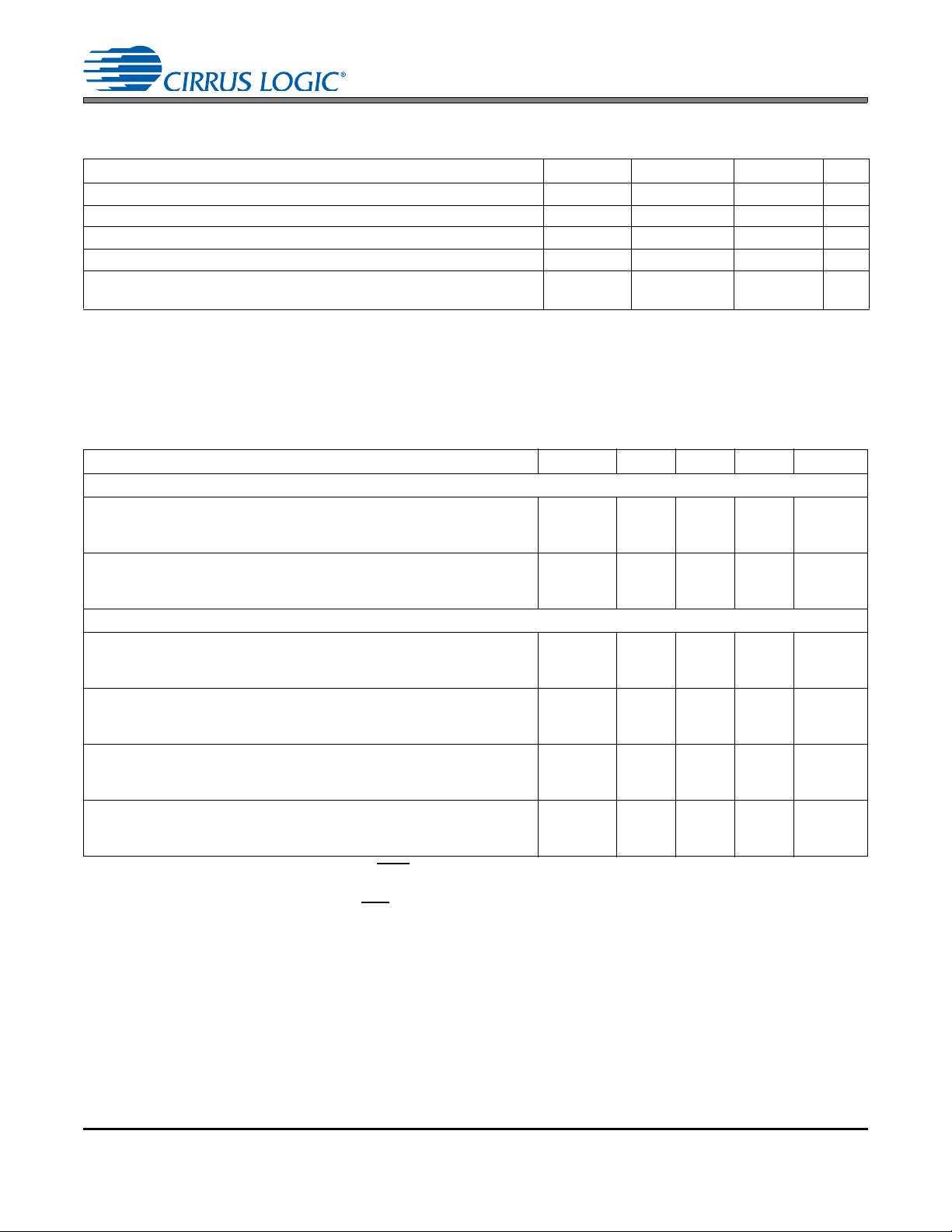
DIGITAL FILTER CHARACTERISTICS
Parameter Min Typ Max Units
Passband (Upsampling or Downsampling) - - 0.4535*Fso Hz
Passband Ripple - - ±0.007 dB
Stopband 0.5465*Fso - - Hz
Stopband Attenuation 125 - - dB
Group Delay SRC Mode
Bypass Mode
3. The equation for the group delay through the sample-rate converter is (56.581 / Fsi) + (55.658 / Fso). For example,
if the input sample rate is 192 kHz and the output sample rate is 96 kHz, the group delay through the sample-rate
converter is (56.581/192,000) + (55.658/96,000) =.875 milliseconds.
-
-
(Note 3)
-
-
3/Fsi
DC ELECTRICAL CHARACTERISTICS
(GND = 0 V; all voltages with respect to 0 V.)
Parameter Symbol Min Typ Max Units
Power-Down Mode (Note 4)
Supply Current in power-down VD
(Oscillator attached to XTI-XTO) VL = 3.3 V
VL = 5.0 V
Supply Current in power-down VD
(Crystal attached to XTI-XTO) VL = 3.3 V
VL = 5.0 V
Normal Operation (Note 5)
Supply Current at 48 kHz Fsi and Fso VD
(Oscillator attached to XTI-XTO) VL = 3.3 V
VL = 5.0 V
Supply Current at 192 kHz Fsi and Fso VD
(Oscillator attached to XTI-XTO) VL = 3.3 V
VL = 5.0 V
Supply Current at 48 kHz Fsi and Fso VD
(Crystal attached to XTI-XTO) VL = 3.3 V
VL = 5.0 V
Supply Current at 192 kHz Fsi and Fso VD
(Crystal attached to XTI-XTO) VL = 3.3 V
VL = 5.0 V
50
100
200
100
1.5
4
24
2.5
4
80
8
13
24
3
7
80
4
6.5
A
A
A
A
mA
mA
mA
mA
mA
mA
mA
mA
mA
mA
mA
mA
mA
mA
s
s
4. Power Down Mode is defined as RST
attached across XTI-XTO, in which case the crystal will begin oscillating.
5. Normal operation is defined as RST
= LOW with all clocks and data lines held static, except when a crystal is
= HI.
DS641F6 11
Page 12

CS8421
DIGITAL INPUT CHARACTERISTICS
Parameters Symbol Min Typ Max Units
Input Leakage Current I
Input Capacitanc e I
in
in
Input Hysteresis -250- mV
--±10A
-8- pF
DIGITAL INTERFACE SPECIFICATIONS
(GND = 0 V; all voltages with respect to 0 V.)
Parameters Symbol Min Max Units
High-Level Output Voltage, except MCLK_OUT and SDOUT (IOH=-4 mA) V
Low-Level Output Voltage, except MCLK_OUT and SDOUT (IOL=4 mA) V
High-Level Output Voltage, MCLK_OUT (I
Low-Level Output Voltage, MCLK_OUT (I
=-6 mA) V
OH
=6 mA) V
OL
High-Level Output Voltage, SDOUT (IOH=-8 mA) V
Low-Level Output Voltage, SDOUT (IOL=8 mA) V
High-Level Input Voltage V
Low-Level Input Voltage V
OH
OL
OH
OL
OH
OL
IH
IL
0.77xVL - V
-.6V
0.77xVL - V
-.6V
0.77xVL - V
-.65V
0.6xVL VL+0.3 V
-0.3 0.8 V
SWITCHING SPECIFICATIONS
(Inputs: Logic 0 = 0 V, Logic 1 = VL; CL = 20 pF)
Parameters Symbol Min Max Units
RST pin Low Pulse Width (Note 6)
XTI Frequency (Note 7) Crystal
Digital Clock Source
XTI Pulse Width High/Low 14.8 - ns
MCLK_OUT Duty Cycle 45 55 %
Slave Mode
I/OSCLK Frequency - 24.576 MHz
OLRCK High Time (Note 8) t
I/OSCLK High Time t
I/OSCLK Low Time t
I/OLRCK Edge to I/OSCLK Rising t
OLRCK Rising Edge to OSCLK Rising Edge (TDM) t
I/OSCLK Rising Edge to I/OLRCK Edge t
OSCLK Rising Edge to OLRCK Falling Edge (TDM) t
OSCLK Falling Edge/OLRCK Edge to SDOUT Output Valid t
SDIN/TDM_IN Setup Time Before I/OSCLK Rising Edge t
SDIN/TDM_IN Hold Time After I/OSCLK Rising Edge t
lrckh
sckh
sckl
lcks
fss
lckd
fsh
dpd
ds
dh
1-ms
16.384
1.024
27.000
27.000
MHz
MHz
326 - ns
9-ns
9-ns
6-ns
5-ns
5-ns
5-ns
-18ns
3.5 - ns
5-ns
12 DS641F6
Page 13

CS8421CS8421
t
ds
OLRCK
(input)
t
dh
t
sckh
t
sckl
t
fsh
t
fss
OSCLK
(input)
TDM_IN
(input)
SDOUT
(output)
MSB
t
dpd
MSB-1
MSB
MSB-1
t
lrckh
t
ds
MSB
t
dh
t
dpd
MSB-1
I/OLRCK
(input)
I/OSCLK
(input)
SDIN
(input)
SDOUT
(output)
MSB
MSB-1
t
sckh
t
sckl
t
lcks
t
lckd
Figure 1. Non-TDM Slave Mode Timing Figure 2. TDM Slave Mode Timing
t
ds
OLRCK
(output)
t
dh
t
dpd
t
fss
OSCLK
(output)
TDM_IN
(input)
SDOUT
(output)
MSB
MSB-1
MSB
MSB-1
t
ds
MSB
t
dh
t
dpd
MSB-1
t
lcks
I/OLRCK
(output)
I/OSCLK
(output)
SDIN
(input)
SDOUT
(output)
MSB
MSB-1
Figure 3. Non-TDM Master Mode Timing Figure 4. TDM Master Mode Timing
Parameters Symbol Min Max Units
Master Mode (Note 9)
I/OSCLK Frequency (non-TDM) 64*Fsi/o MHz
OSCLK Frequency (TDM) 256*Fso MHz
I/OLRCK Duty Cycle 45 55 %
I/OSCLK Duty Cycle 45 55 %
I/OSCLK Falling Edge to I/OLRCK Edge t
OSCLK Falling Edge to OLRCK Edge (TDM) t
OSCLK Falling Edge to SDOUT Output Valid t
SDIN/TDM_IN Setup Time Before I/OSCLK Rising Edge t
SDIN/TDM_IN Hold Time After I/OSCLK Rising Edge t
lcks
fss
dpd
ds
dh
-5ns
-5ns
-7ns
3-ns
5-ns
6. After powering up the CS8421, RST should be held low until the power supplies and clocks are settled.
7. The maximum possible sample rate is XTI/128.
8. OLRCK must remain high for at least 8 OSCLK periods in TDM Mode.
9. Only the input or the output serial port can be set as master at a given time.
DS641F6 13
Page 14

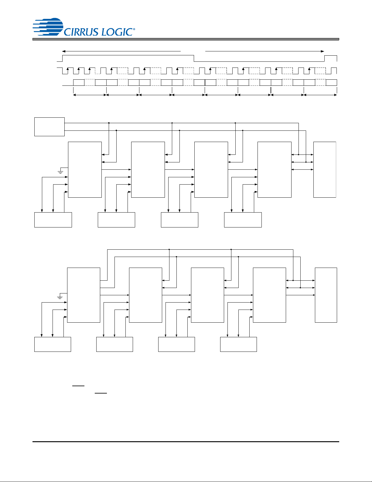
3. TYPICAL CONNECTION DIAGRAMS
CS8421
VD VL
Serial
Audio
Source
ILRCK
ISCLK
SDIN
BYPASS
+2.5 V +3.3 V or +5.0 V
0.1 F0.1 F
Serial
Audio
Input
Device
OLRCK
OSCLK
SDOUT
XTI
RST
SRC_UNLOCK
SAOF
TDM_IN
Hardware Control
Settings
GND
SAIF
MS_SEL
GND
**
1 k
*
***
Figure 5. Typical Connection Diagram, No External Master Clock
* When no external master clock is supplied to the part, both input and output must be set to Slave Mode for the
part to operate properly. This is done by conn ecting the MS_SEL pin to grou nd through a resistance of 0
to 1 k
+ 1% as stated in Table 1, “Serial Audio Port Master/Slave and Clock Ratio Select Start-Up Options (MS_SEL),”
on page 18.
** The connection (VL or GND) and value of these two resistors determines the mode of opera tion for the input and
output serial ports as described in Table 2 on page 18 and Table 3 on page 18.
*** This pin must not be pulled high. See Section 1, “Pin Descriptions.”
CS8421
14 DS641F6
Page 15

CS8421CS8421
CS8421
VD VL
Serial
Audio
Source
ILRCK
ISCLK
SDIN
BYPASS
+2.5 V +3.3 V or + 5 .0 V
0.1 F0.1 F
Serial
Audio
Input
Device
OLRCK
OSCLK
SDOUT
XTI
XTO
RST
SRC_UNLOCK
SAOF
TDM_IN
Hardware Control
Settings
Crysta l /C loc k
Source
GND
SAIF
MS_SEL
GND
MCLK_OUT
To extern a l
hardware
47 k
* **
***
Figure 6. Typical Connection Diagram, Master and Slave Modes
* The connection (VL or GND) and value of these three resistors determines the mode of operation for the input
and output serial ports as described in Table 1 Serial Audio Port Master/Slave and Clock Ratio Select Start-Up Op-
tions (MS_SEL), and Table 2, “Serial Audio Input Port St art-Up Options (SAIF),” on page 18 and Table 3, “Serial
Audio Output Port Start-Up Options (SAOF),” on page 18.
** MCLK_OUT pin should be pulled high through a 47 k
resistor if an MCLK output is not needed.
*** This pin must not be pulled high. See Section 1, “Pin Descriptions.”
DS641F6 15
Page 16

CS8421
4. APPLICATIONS
The CS8421 is a 32-bit, high-performance, monolith ic CM OS ste re o asynchronous sample-rate converter.
The digital audio data is input and output through configurable 3-wire serial ports. The d igital audio input/output ports
offer Left-Justified, Right-Justified, and I²S serial audio formats. The CS8421 also supports a TDM Mode which allows multiple channels of digital audio data on one serial line. A Bypass Mode allows the data to be passed directly
to the output port without sample rate conversion.
The CS8421 does not require a control port interface, help i ng to speed design time by not requiring the user to d evelop software to configure the part. Pins that are sensed after reset allow the part to be configured. See “Reset,
Power-Down, and Start-Up” on page 22.
Target applications include digital recording systems (DVD-R/RW, CD-R/RW, PVR, DAT, MD, and VTR), digital mixing consoles, high quality D/A, effects processors and computer audio systems.
Figure 5 and 6 show the supply and external connections to the CS8421.
4.1 Three-wire Serial Input/Output Audio Port
A 3-wire serial audio input/output port is provided. The interface format should be chosen to suit the attached device
through the MS_SEL, SAIF, and SAOF pins. Tables 1, 2, and 3 show the pin functions and their corresponding settings. The following parameters are adjustable:
• Master or Slave
• Master clock (MCLK) frequencies of 128*Fsi/o, 256*Fsi/o, 384*Fsi/o, and 512*Fsi/o (Master Mode)
• Audio data resolution of 16-, 20-, 24-, or 32-bits
• Left- or Right-Justification of the data relative to left/right clock (LRCK) as well as I²S
Figures 7, 8, and 9 show the input/output formats available.
In Master Mode, the left/right clock and the serial bit clock are outputs, derived from the XTI input pin master clock.
In Slave Mode, the left/right clock and the serial bit clock are inputs and may be asynchronous to the XTI master
clock. The left/right clock should be continuous, but the duty cycle can be less than 50% if enough serial clocks are
present in each phase to clock all of the data bits.
ISCLK is always set to 64*Fsi when the input is set to master. In no rmal operation, OSCL K is set to 64 *Fso. In TDM
Slave Mode, OSCLK must operate at N*64*Fso, where N is the number of CS8421’s connected together. In TDM
Master Mode, OSCLK is set to 256*Fso
For more information about serial audio formats, refer to th e Cirrus Logic applications no te AN282, “The 2-Channel
Serial Audio Interface: A Tutorial”, available at www.cirrus.com
.
16 DS641F6
Page 17

CS8421CS8421
I/OLRCK
I/OSCLK
MSB LSB
MSB
LSB
Channel A
SDIN
SDOUT
MSB
Channel B
Figure 7. Serial Audio Interface Format - I²S
MSB LSB
MSB
LSB
MSB
I/OLRCK
I/OSCLK
SDIN
SDOUT
Channel A Channel B
Figure 8. Serial Audio Interface Format - Left-Justified
I/OLRCK
I/OSCLK
Channel A
SDIN
Channel B
MSB
SDOUT
MSB
MSB
MSB LSB
LSB
LSB
LSB
MSB Extended MSB Extended
Figure 9. Serial Audio Interface Format - Right-Justified
4.2 Mode Selection
The CS8421 uses the resistors attached to the MS_SEL, SAIF, and SAOF pins to determine the mod es of operation.
After reset, the resistor value and condition (VL or GND) are sensed. This operation will take approximately 4
complete. The SRC_UNLOCK pin will remain high and the SDOUT pin will be muted until the mode detection sequence has completed. After this, if all clocks are stable, SRC_UNLOCK will be brought low when audio output is
valid and normal operation will occur. Tables1, 2, and 3 show the pin functions and their corresponding settings. If
the 1.0 k
option is selected for MS_SEL, SAIF, or SAOF, the resistor connected to that pin may be replaced by a
direct connection to VL or GND as appropriate.
The resistor attached to each mode-selection pin should be placed physically close to the CS8421. The end of the
resistor not connected to the mode selection pins should be connected as close as possible to VL and GND to minimize noise. Tables 1, 2, and 3 show the pin functions and their corresponding settings.
s to
DS641F6 17
Page 18

CS8421
MS_SEL pin Input M/S Output M/S
1.0 k ± 1% to GND Slave Slave
1.96 k ± 1% to GND Slave
4.02 k ± 1% to GND Slave
8.06 k ± 1% to GND Slave
16.2 k ± 1% to GND Slave
1.0 k ± 1% to VL
1.96 k ± 1% to VL
4.02 k ± 1% to VL
8.06 k ± 1% to VL
Master (
Master (
Master (
Master (
128 x Fsi)
256 x Fsi)
384 x Fsi)
512 x Fsi)
Table 1. Serial Audio Port Master/Slave and Clock Ratio Select Start-Up Options (MS_SEL)
SAIF pin Input Port Configuration
1.0 k ± 1% to GND I²S up to 32-bit data
1.96 k ± 1% to GND Left-Justified up to 32-bit data
4.02 k ± 1% to GND Right-Justi fied 16-bit data
1.0 k ± 1% to VL Right-Justified 20-bit data
1.96 k ± 1% to VL Right-Justified 24-bit data
4.02 k ± 1% to VL Right-Justified 32-bit data
Table 2. Serial Audio Input Port Start-Up Options (SAIF)
Master (
Master (
Master (
Master (
128 x Fso)
256 x Fso)
384 x Fso)
512 x Fso)
Slave
Slave
Slave
Slave
SAOF pin Output Port Configuration
1.0 k ± 1% to GND I²S 16-bit data
1.96 k ± 1% to GND I ²S 20-bit data
4.02 k ± 1% to GND I ²S 24-bit data
8.06 k ± 1% to GND I ²S 32-bit data
16.2 k ± 1% to GND Left-Justified 16-bit data
32.4 k ± 1% to GND Left-Justified 20-bit data
63.4 k ± 1% to GND Left-Justified 24-bit data
127.0 k ± 1% to GND Left-Justified 32-bit data
1.0 k ± 1% to VL Right-Justified 16-bit data
1.96 k ± 1% to VL Right-Justified 20-bit data
4.02 k ± 1% to VL Right-Justified 24-bit data
8.06 k ± 1% to VL Right-Justified 32-bit data
16.2 k ± 1% to VL TDM Mode 16-bit data
32.4 k ± 1% to VL TDM Mode 20-bit data
63.4 k ± 1% to VL TDM Mode 24-bit data
127.0 k ± 1% to VL TDM Mode 32-bit data
Table 3. Serial Audio Output Port Start-Up Options (SAOF)
18 DS641F6
Page 19

4.3 Sample Rate Converter (SRC)
Multirate digital signal processing techniques are used to conceptually up sample the incoming data to a very
high rate and then downsample to the outgoing rate. The internal data path is 32-bits wide even if a lower
bit depth is selected at the output. The filtering is designed so that a full inpu t a udio ban dwidth of 20 kHz is
preserved if the input sample and output sample rates are greater than or equal to 4 4.1 kHz. When the output sample rate becomes less than the input sample rate, the input is automatically band-limited to avoid
aliasing products in the output. Careful design ensures minimum ripple and distortion products are added
to the incoming signal. The SRC also determines the ratio between the incoming and outgoing sample rates
and sets the filter corner frequencies appropriately. Any jitter in the incoming signal has little impact on the
dynamic performance of the rate converter and has no influ ence on the output clock.
4.3.1 Data Resolution and Dither
When using the serial audio input port in Left-Justified and I²S Modes, all input data is treate d as 32 -bits
wide. Any truncation that has been done prior to the CS8421 to less than 32-bits should have been done
using an appropriate dithering process. If the serial audio input port is in Right-Justified Mode, the input
data will be truncated to the bit depth set by SAIF pin setting. If the SAIF bit depth is set to 16-, 20-, or 24bits, and the input data is 32-bits wide, truncation distortion will occur. Similarly, in any serial audio input
port mode, if an inadequate number of bit clocks are entered (i.e. 16 clocks instead of 20 clocks), the input
words will be truncated, causing truncation distortion at low levels. In summary, there is no dithering
mechanism on the input side of the CS8421, and care must be taken to ensure th at no trunca tion occurs.
CS8421CS8421
Dithering is used internally where appropriate inside the SRC block.
The output side of the SRC can be set to 16-, 20-, 24-, or 32-bits. Dithering is applied and is automatically
scaled to the selected output word length. This dither is not correlated between left and right channels.
4.3.2 SRC Locking and Varispeed
The SRC calculates the ratio between the input sample rate and the outp ut sample rate and uses this information to set up various parameters inside the SRC block. The SRC takes some time to make this calculation, approximately 4200/Fso (87.5 ms at Fso of 48 kHz).
If Fsi is changing, as in a varispeed application, the SRC will track the incoming sample rate. During this
tracking mode, the SRC will still rate convert the audio data, but at increased distortion levels. Once the
incoming sample rate is stable, the SRC will return to normal levels of audio quality. The data buffer in the
SRC can overflow if the input sample rate changes at greater than 10%/sec. There is no provision for
varispeed applications where Fso is changing.
The SRC_UNLOCK pin is used to indicate when the SRC is not locked. When RST
is a change in Fsi or Fso, SRC_UNLOCK will be set high. The SRC_UNLOCK pin will continue to be high
until the SRC has reacquired lock and settled, at which point it will transition low. When the
SRC_UNLOCK pin is set low, SDOUT is outputting valid audio data. This can b e used to signal a DAC to
unmute its output.
4.3.3 Bypass Mode
When the BYPASS pin is set high, the input data bypasses the sample rate converter and is sent directly
to the serial audio output port. No dithering is performed on the outp ut data. This mode is ideal for passing
non-audio data through without a sample-rate conversion. ILRCK and OLRCK should be the same sample rate and synchronous in this mode. The group delay in this mode is greatly reduced from normal SRC
mode as noted in the “Digital Filter Characteristics” on page 11.
is asserted, or if there
DS641F6 19
Page 20

4.3.4 Muting
The SDOUT pin is set to all zero output (full mute) immediately after the RST pin is set high. When the
output from the SRC becomes valid, though the SRC may not have reached full performance, SDOUT is
unmuted over a period of approximately 4096 OLRCK cycles (soft unmuted). When the output becomes
invalid, depending on the condition, SDOUT is either immediately set to all zero output (hard muted) or
SDOUT is muted over a period of approximately 4096 OLRCK cycles until it reaches full mute (soft muted). The SRC will soft mute SDOUT if there is an illegal ratio between ILRCK and the XTI master clock.
Conditions that will cause the SRC to hard mute SDOUT include removing OLRCK, the RST
set low, or illegal ratios between OLRCK and the XTI master clock. After all invalid states have been
cleared, the SRC will soft unmute SDOUT.
4.3.5 Group Delay and Phase Matching Between Multiple CS8421 Parts
The equation for the group delay through the sample rate converter is shown in “Digital Filter Character-
istics” on page 11. This phase delay is equal across multiple parts. Therefore, when multiple parts operate
at the same Fsi and Fso and use a common XTI/XTO clock, their output data is phase matched.
4.3.6 Master Clock
The CS8421 uses the clock signal supplied through XTI as its mast er clock (MCLK). MCLK can be supplied from a digital clock source, a crystal oscillator, or a fundamental mode crystal. Figure 10 shows the
typical connection diagram for using a fundamental mode crystal. Please refer t o th e cr yst al ma nufa ct ur er’s specifications for the external capacitor recommendations. If XTO is not used, such as with a digital
clock source or crystal oscillator, XTO should be left unconnected or pulled low through a 47 k
to GND.
CS8421
pin being
resistor
If either serial audio port is set as master, MCLK will be used to supply the sub-clocks to the master SCLK
and LRCK. In this case, MCLK will be synchronous to the master serial audio port. If both serial audio
ports are set as slave, MCLK can be asynchronous to either or both ports. If the user needs to change the
clock source to XTI while the CS8421 is still powered on and running, a RESET must be issued once the
XTI clock source is present and valid to ensure proper operation.
When both serial ports are configured as slave and operating at sample rates less than 96 kHz, the
CS8421 has the ability to operate without a master clock input through XTI. This benefits the design by
not requiring extra external clock components (lowering production cost) and not requiring a master clock
to be routed to the CS8421, resulting in lowered noise contribution in the system. In this mode, an internal
oscillator provides the clock to run all of the internal logic. To enable the internal oscillator, simply tie XTI
to GND or VL. In this mode, XTO should be left unconnected.
The CS8421 can also provide a buffered MCLK output through the MCLK_O UT pin. This pin can be used
to supply MCLK to other system components that operate synchronously to MCLK. If MCLK_OUT is not
needed, the output of the pin can be disabled by pulling the pin high through a 47 k
MCLK_OUT is also disabled when using the internal oscillator mode. The MCLK_OUT pin will be set low
when disabled by using the internal oscillator mode.
resistor to VL.
20 DS641F6
Page 21

4.3.7 Clocking
XTI XTO
CC
R
Figure 10. Typical Connection Diagram for Crystal Circuit
OLRCK
OSCLK
LSBMSB LSBMSB LSBMSB LSBMSB LSBMSB LSBMSB
SDOUT/
TDM_IN
SDOUT 3, ch A
32 clks 32 clks 32 clks 32 clks 32 clks 32 clks
LSBMSB LSBMSB
32 clks 32 clks
SDOUT 3, ch B SDOUT 2, ch A SDOUT 2, ch B SDOUT 1, ch A SDOUT 1, ch B
SDOUT 4, ch A SDOUT 4, ch B
Figure 11. TDM Slave Mode Timing Diagram
In order to ensure proper operation of the CS8421, the clock or crystal attached to XTI must simultaneously satisfy the requirements of LRCK for both the input and output as follows:
CS8421CS8421
• If the input is set to master, Fsi
• If the output is set to master, Fso
• If b oth inpu t and output are set to slave, XTI
XTI/128 and Fso XTI/130.
XTI/128 and Fsi XTI/130.
130*[maximum(Fsi,Fso)], XTI/Fsi < 3750, and XTI/Fso <
3750.
4.4 Time Division Multiplexing (TDM) Mode
TDM Mode allows several CS8421 to be serially connected together allowing their corresponding SDOUT
data to be multiplexed onto one line for input into a DSP or other TDM-capable multichannel device.
The CS8421 can operate in two TDM modes. The first mode consists of all of the CS8421’s output ports set
to slave, as shown in Figure 13. The second mode consists of one CS8421 output port set to master and
the remaining CS8421’s output ports set to slave, as shown in Figure 14.
The TDM_IN pin is used to input the data, while the SDOUT pin is used to output the data. The first CS8421
in the chain should have its TDM_IN set to GND. Data is transmitted from SDOUT most significant bit first
on the first OSCLK falling edge after an OLRCK transition and is valid on the rising edge of OSCLK.
In TDM Slave Mode, the number of channels that can by multiplexed to one serial data line depends on the
output sampling rate. For Slave Mode, OSCLK must operate at N*64*Fso, where N is the number of
CS8421’s connected together. The maximum allowable OSCLK frequency is 24.576 MHz, so for Fso =
48 kHz, N = 8 (16 channels of serial audio data).
In TDM Master Mode, OSCLK operates at 256*Fso, which is equivalent to N = 4 , so a maximum o f 8 channels of digital audio can be multiplexed together. Note that for TDM Master Mode, MCLK must be at least
256*Fso, where Fso
with the valid data sample left-justified within the time-slot. Valid data lengths are 16-, 20-, 24- or 32-bits.
Figures 11 and 12 show the interface format for Master and Slave TDM Modes with a 32-bit word-length.
DS641F6 21
96 kHz. OLRCK identifies the start of a new frame. Each time-slot is 32-bits wide,
Page 22
CS8421
OLRCK
OSCLK
LSBMSB LSBMSB LSBMSB LSBMSB LSBMSB LSBMSB
SDOUT/
TDM_IN
SDOUT 3, ch A
32 clks 32 clks 32 clks 32 clks 32 clks 32 clks
LSBMSB LSBMSB
32 clks 32 clks
SDOUT 3, ch B SDOUT 2, ch A SDOUT 2, ch B SDO UT 1, ch A SDOUT 1, ch B
SDOUT 4, ch A SDOUT 4, ch B
256 OSCLKs
Figure 12. TDM Master Mode Timing Diagram
ILRCK
ISCLK
SDIN
OLRCK
OSCLK
SDOUTTDM_IN
OLRCK
OSCLK
SDOUTTDM_IN
ILRCK
ISCLK
SDIN
Output
Clock
Source
LRCK
SCLK
OLRCK OSCLK SDOUT
PCM Source 2
OLRCK OSCLK SDOUT
PCM Source 1
CS8421
1
Slave
CS8421
2
Slave
LRCK
SCLK
SDIN
DSP
Slave
OLRCK
OSCLK
SDOUTTDM_IN
ILRCK
ISCLK
SDIN
CS8421
3
Slave
OLRCK
OSCLK
SDOUTTDM_IN
ILRCK
ISCLK
SDIN
CS8421
4
Slave
OLRCK OSCLK SDOUT
PCM Source 3
OLRCK OSCLK SDOUT
PCM Source 4
Figure 13. TDM Mode Configuration (All CS8421 Outputs are Slave)
ILRCK
ISCLK
SDIN
OLRCK
OSCLK
SDOUTTDM_IN
CS8421
1
OLRCK OSCLK SDOUT
PCM Source 2
OLRCK OSCLK SDOUT
PCM Source 1
Master
LRCK
SCLK
SDIN
DSP
Slave
OLRCK
OSCLK
SDOUTTDM_IN
ILRCK
ISCLK
SDIN
CS8421
4
Slave
OLRCK
OSCLK
SDOUTTDM_IN
ILRCK
ISCLK
SDIN
CS8421
2
Slave
OLRCK
OSCLK
SDOUTTDM_IN
ILRCK
ISCLK
SDIN
CS8421
3
Slave
OLRCK OSCLK SDOUT
PCM Source 3
OLRCK OSCLK SDOUT
PCM Source 4
Figure 14. TDM Mode Configuration (First CS8421 Output is Master, All Others are Slave)
4.5 Reset, Power-Down, and Start-Up
When RST is low, the CS8421 enters a low-power mode, all internal states are reset, and the outputs are
disabled. After RST
22 DS641F6
(MS_SEL, SAIF, and SAOF) and sets the appropriate mode of operation. After the mo de has been set (approximately 4
transitions from low to high, the part sens es the resistor value on the configuration pins
s), the part is set to normal operation and all outputs are functional.
Page 23

4.6 Power Supply, Grounding, and PCB Layout
The CS8421 operates from a VD = +2.5 V and VL = +3.3 V or +5.0 V supply. These supplies may be set
independently. Follow normal supply decoupling practices; see Figure 6.
Extensive use of power and ground planes, ground-plane fill in unused areas, and surface-mount decoupling capacitors are recommended. Decoupling capacitors should be mounted on the same side of the
board as the CS8421 to minimize inductance effects, and all decoupling capacitors should be as close to
the CS8421 as possible. The pin of the configuration resistors not connecte d to MS_SEL, SAIF, and SAOF
should be connected as close as possible to VL or GND.
The CS8421 is available in the compact QFN package. The undersi de of the QFN pa ckage reveals a metal
pad that serves as a thermal relief to provide for optimal heat dissipation. This pad must m ate with an equally
dimensioned copper pad on the PCB and must be electrically connected to ground. A series of vias should
be used to connect this copper pad to one or more larger ground planes on other PCB layers.
CS8421CS8421
DS641F6 23
Page 24
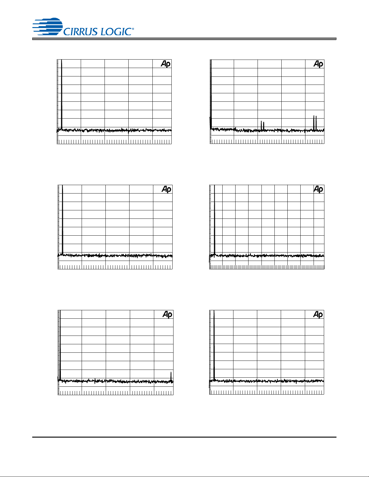
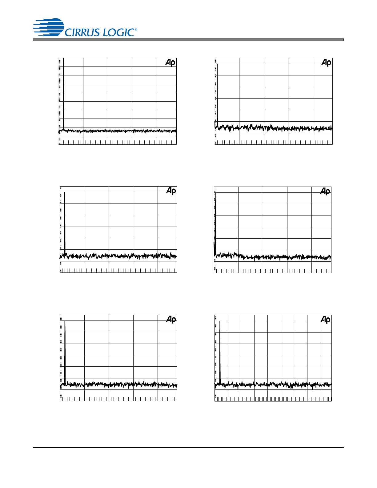
5. PERFORMANCE PLOTS
-200
+0
-180
-160
-140
-120
-100
-80
-60
-40
-20
d
B
F
S
5k 20k10k 15k
Hz
-200
+0
-180
-160
-140
-120
-100
-80
-60
-40
-20
d
B
F
S
20k 80k40k 60k
Hz
Figure 15. Wideband FFT Plot (16k Points) 0 dBFS 1 kHz Tone, 48 kHz:48 kHz
-200
+0
-180
-160
-140
-120
-100
-80
-60
-40
-20
d
B
F
S
5k 20k10k 15k
Hz
-200
+0
-180
-160
-140
-120
-100
-80
-60
-40
-20
d
B
F
S
2.5k 20k5k 7.5k 10k 12.5k 15k 17.5k
Hz
Figure 17. Wideband FFT Plot (16k Points) 0 dBFS 1 kHz Tone, 44.1 kHz:48 kHz
-200
+0
-180
-160
-140
-120
-100
-80
-60
-40
-20
d
B
F
S
10k 40k20k 30k
Hz
Figure 19. Wideband FFT Plot (16k Points) 0 dBFS 1 kHz Tone, 48 kHz:96 kHz
CS8421
+0
-20
-40
-60
-80
d
B
-100
F
S
-120
-140
24 DS641F6
-160
-180
-200
5k 20k10k 15k
Hz
Page 25
-200
+0
-180
-160
-140
-120
-100
-80
-60
-40
-20
d
B
F
S
5k 20k10k 15k
Hz
Figure 21. Wideband FFT Plot (16k Points) 0 dBFS 1 kHz Tone, 192 kHz:48 kHz
Figure 23. Wideband FFT Plot (16k Points) - 60 dBFS 1 kHz Tone, 48 kHz:48 kHz
-200
-60
-180
-160
-140
-120
-100
-80
d
B
F
S
5k 20k10k 15k
Hz
Figure 25. Wideband FFT Plot (16k Points) - 60 dBFS 1 kHz Tone, 44.1 kHz:48 kHz
CS8421CS8421
-60
-80
-100
d
-120
B
F
S
-140
-160
-180
-200
-60
-80
-100
d
-120
B
F
S
-140
-160
-180
-200
5k 20k10k 15k
Hz
-60
-80
-100
d
-120
B
F
S
-140
-160
-180
-200
-60
10k 40k20k 30k
Hz
20k 80k40k 60k
Hz
-80
-100
d
-120
B
F
S
-140
-160
DS641F6 25
-180
-200
2.5k 20k5k 7.5k 10k 12.5k 15k 17.5k
Hz
Page 26

-200
-60
-180
-160
-140
-120
-100
-80
d
B
F
S
5k 20k10k 15k
Hz
Figure 27. Wideband FFT Plot (16k Points) - 60 dBFS 1 kHz Tone, 96 kHz:48 kHz
-200
-60
-180
-160
-140
-120
-100
-80
d
B
F
S
5k 20k10k 15k
Hz
Figure 29. Wideband FFT Plot (16k Points) - 60 dBFS 1 kHz Tone, 192 kHz:48 kHz
-200
+0
-180
-160
-140
-120
-100
-80
-60
-40
-20
d
B
F
S
5k 20k10k 15k
Hz
-200
+0
-180
-160
-140
-120
-100
-80
-60
-40
-20
d
B
F
S
5k 20k10k 15k
Hz
Figure 31. IMD, 10 kHz and 11 kHz -7 dBFS, 44.1 kHz:48 kHz
CS8421
+0
-20
-40
-60
-80
d
B
-100
F
S
-120
-140
-160
-180
-200
+0
-20
-40
-60
-80
d
B
-100
F
S
-120
-140
-160
-180
-200
5k 20k10k 15k
Hz
2.5k 20k5k 7.5k 10k 12.5k 15k 17.5k
Hz
26 DS641F6
Page 27

-200
+0
-180
-160
-140
-120
-100
-80
-60
-40
-20
d
B
F
S
20k 80k40k 60k
Hz
Figure 33. Wideband FFT Plot (16k Points) 0 dBFS 80 kHz Tone, 192 kHz:192 kHz
-200
+0
-180
-160
-140
-120
-100
-80
-60
-40
-20
d
B
F
S
5k 20k10k 15k
Hz
-200
+0
-180
-160
-140
-120
-100
-80
-60
-40
-20
d
B
F
S
5k 20k10k 15k
Hz
Figure 35. Wideband FFT Plot (16k Points) 0 dBFS 20 kHz Tone, 48 kHz:48 kHz
Figure 37. Wideband FFT Plot (16k Points) 0 dBFS 20 kHz Tone, 48 kHz:44.1 kHz
CS8421CS8421
+0
-20
-40
-60
-80
d
B
-100
F
S
-120
-140
-160
-180
-200
10k 40k20k 30k
Hz
+0
-20
-40
-60
-80
d
B
-100
F
S
-120
-140
DS641F6 27
-160
-180
-200
2.5k 20k5k 7.5k 10k 12.5k 15k 17.5k
Hz
-120
-122.5
-125
-127.5
-130
-132.5
d
B
-135
F
S
-137.5
-140
-142.5
-145
-147.5
-150
50k 175k75k 100k 125k 150k
Hz
Page 28

-150
-120
-147.5
-145
-142.5
-140
-137.5
-135
-132.5
-130
-127.5
-125
-122.5
d
B
F
S
50k 175k75k 100k 125k 150k
Hz
Figure 39. THD+N vs. Output Sample Rate, 0 dBFS 1 kHz Tone, Fsi = 48 kHz
Figure 41. THD+N vs. Output Sample Rate, 0 dBFS 1 kHz Tone, Fsi = 44.1 kHz
-150
-120
-147.5
-145
-142.5
-140
-137.5
-135
-132.5
-130
-127.5
-125
-122.5
d
B
F
S
50k 175k75k 100k 125k 150k
Hz
Figure 43. THD+N vs. Output Sample Rate, 0 dBFS 1 kHz Tone, Fsi = 32 kHz
d
B
F
S
-120
-122.5
-125
-127.5
-130
-132.5
-135
-137.5
-140
-142.5
-145
-147.5
-150
CS8421
50k 175k75k 100k 125k 150k
Hz
-120
-122.5
-125
-127.5
-130
-132.5
d
B
-135
F
S
-137.5
-140
-142.5
-145
-147.5
-150
50k 175k75k 100k 125k 150k
28 DS641F6
Hz
-135
-136
-137
-138
-139
d
B
-140
F
S
-141
-142
-143
-144
-145
-120
-122.5
-125
-127.5
-130
-132.5
d
B
-135
F
S
-137.5
-140
-142.5
-145
-147.5
-150
50k 175k75k 100k 125k 150k
50k 175k75k 100k 125k 150k
Hz
Hz
Page 29

-150
-120
-147.5
-145
-142.5
-140
-137.5
-135
-132.5
-130
-127.5
-125
-122.5
d
B
F
S
50k 175k75k 100k 125k 150k
Hz
Figure 45. Dynamic Range vs. Output Sample Rate, -60 dBFS 1 kHz Tone, Fsi = 96 kHz
-140
+0
-120
-100
-80
-60
-40
-20
d
B
F
S
0 60k10k 20k 30k 40k 50k
Hz
192 kHz:32 kHz
192 kHz:48 kHz
192 kHz:96 kHz
Figure 47. Frequency Response with 0 dBFS Input Figure 48. Passband Ripple, 192 kHz:48 kHz
Figure 49. Dynamic Range vs. Output Sample Rate, -60 dBFS 1 kHz Tone, Fsi = 48 kHz
-120
-122.5
-125
-127.5
-130
-132.5
d
B
-135
F
S
-137.5
-140
-142.5
-145
-147.5
-150
50k 175k75k 100k 125k 150k
+0
-0.02
-0.04
-0.06
-0.08
d
B
-0.1
F
S
-0.12
-0.14
-0.16
-0.18
-0.2
0 25k5k 10k 15k 20k
Hz
Hz
CS8421CS8421
-120
-122.5
-125
-127.5
-130
-132.5
d
B
-135
F
S
-137.5
-140
-142.5
-145
-147.5
-150
50k 175k75k 100k 125k 150k
Hz
DS641F6 29
+0
-10
-20
-30
-40
-50
d
-60
B
-70
F
S
-80
-90
-100
-110
-120
-130
-140
-140 +0-120 -100 -80 -60 -40 -20
dBFS
Page 30

-140
+0
-130
-120
-110
-100
-90
-80
-70
-60
-50
-40
-30
-20
-10
d
B
F
S
-140 +0-120 -100 -80 -60 -40 -20
dBFS
Figure 51. Linearity Error, 0 to -140 dBFS Input, 200 Hz Tone, 48 kHz:44.1 kHz
-140
+0
-130
-120
-110
-100
-90
-80
-70
-60
-50
-40
-30
-20
-10
d
B
F
S
-140 +0-120 -100 -80 -60 -40 -20
dBFS
-140
+0
-130
-120
-110
-100
-90
-80
-70
-60
-50
-40
-30
-20
-10
d
B
F
S
-140 +0-120 -100 -80 -60 -40 -20
dBFS
Figure 53. Linearity Error, 0 to -140 dBFS Input, 200 Hz Tone, 96 kHz:48 kHz
-140
+0
-130
-120
-110
-100
-90
-80
-70
-60
-50
-40
-30
-20
-10
d
B
F
S
-140 +0-120 -100 -80 -60 -40 -20
dBFS
-140
+0
-130
-120
-110
-100
-90
-80
-70
-60
-50
-40
-30
-20
-10
d
B
F
S
-140 +0-120 -100 -80 -60 -40 -20
dBFS
Figure 55. Linearity Error, 0 to -140 dBFS Input, 200 Hz Tone, 44.1 kHz:48 kHz
+0
-10
-20
-30
-40
-50
d
-60
B
-70
F
S
-80
-90
-100
-110
-120
-130
-140
-140 +0-120 -100 -80 -60 -40 -20
dBFS
CS8421
30 DS641F6
Page 31

-180
-110
-175
-170
-165
-160
-155
-150
-145
-140
-135
-130
-125
-120
-115
d
B
F
S
-140 +0-120 -100 -80 -60 -40 -20
dBFS
Figure 57. THD+N vs. Input Amplitude, 1 kHz Tone, 48 kHz:44.1 kHz
-180
-110
-175
-170
-165
-160
-155
-150
-145
-140
-135
-130
-125
-120
-115
d
B
F
S
-140 +0-120 -100 -80 -60 -40 -20
dBFS
-180
-110
-175
-170
-165
-160
-155
-150
-145
-140
-135
-130
-125
-120
-115
d
B
F
S
-140 +0-120 -100 -80 -60 -40 -20
dBFS
Figure 59. THD+N vs. Input Amplitude, 1 kHz Tone, 96 kHz:48 kHz
-180
-110
-175
-170
-165
-160
-155
-150
-145
-140
-135
-130
-125
-120
-115
d
B
F
S
-140 +0-120 -100 -80 -60 -40 -20
dBFS
-180
-110
-175
-170
-165
-160
-155
-150
-145
-140
-135
-130
-125
-120
-115
d
B
F
S
-140 +0-120 -100 -80 -60 -40 -20
dBFS
Figure 61. THD+N vs. Input Amplitude, 1 kHz Tone, 44.1 kHz:48 kHz
-110
-115
-120
-125
-130
-135
-140
d
B
-145
F
S
-150
-155
-160
-165
-170
-175
-180
-140 +0-120 -100 -80 -60 -40 -20
dBFS
CS8421CS8421
DS641F6 31
Page 32

-180
-110
-175
-170
-165
-160
-155
-150
-145
-140
-135
-130
-125
-120
-115
d
B
F
S
0 20k2.5k 5k 7.5k 10k 12.5k 15k 17.5k
Hz
-180
-110
-175
-170
-165
-160
-155
-150
-145
-140
-135
-130
-125
-120
-115
d
B
F
S
-140 +0-120 -100 -80 -60 -40 -20
dBFS
Figure 63. THD+N vs. Frequency Input, 0 dBFS, 48 kHz:44.1 kHz
Figure 65. THD+N vs. Frequency Input, 0 dBFS, 44.1 kHz:48 kHz
CS8421
-110
-115
-120
-125
-130
-135
-140
d
B
-145
F
S
-150
-155
-160
-165
-170
-175
-180
0 20k2.5k 5k 7.5k 10k 12.5k 15k 17.5k
Hz
-110
-115
-120
-125
-130
-135
-140
d
B
-145
F
S
-150
-155
-160
-165
-170
-175
-180
0 20k2.5k 5k 7.5k 10k 12.5k 15k 17.5k
Hz
All performance plots represent typical performance. Measurements for all performance plots were taken und er the
following conditions, unless otherwise stated:
• VD = 2.5 V, VL = 3.3 V
• Serial Audio Input port set to slave
• Serial Audio Output port set to slave
• Input and output clocks and data are asynchronous
• XTI/XTO = 27 MHz
• Input signal = 1.000 kHz, 0 dBFS
• Measurement Bandwidth = 20 to (Fso/2) Hz
• Word Width = 24 Bits
32 DS641F6
Page 33

6. PACKAGE DIMENSIONS
20L TSSOP (4.4 MM BODY) PACKAGE DRAWING
E
N
1
23
e
b
2
A1
A2
A
D
SEATING
PLANE
E1
1
L
SIDE VIEW
END VIEW
TOP VIEW
CS8421CS8421
INCHES MILLIMETERS
DIM MIN NOM MAX MIN NOM MAX
A -- -- 0.043 -- -- 1.10
A1 0.002 0.004 0.006 0.05 -- 0.15
A2 0.03346 0.0354 0.037 0.85 0.90 0.95
b 0.00748 0.0096 0.012 0.19 0.245 0.30 2,3
D 0.252 0.256 0.259 6.40 6.50 6.60 1
E 0.248 0.2519 0.256 6.30 6.40 6.50
E1 0.169 0.1732 0.177 4.30 4.40 4.50 1
e -- -- 0.026 -- -- 0.65
L 0.020 0.024 0.028 0.50 0.60 0.70
µ
0° 4° 8° 0° 4° 8°
JEDEC #: MO-153
Controlling Dimension is Millimeters.
Notes:
1. “D” and “E1” are reference datums and do not included mold flash or protrusions, but do in clude mold mismatch
and are measured at the parting line, mold flash or protrusions shall not exceed 0.20 mm per side.
2. Dimension “b” does not include dambar protrusion/intrusion. Allowable dambar protrusion shall be 0.13 mm total in
excess of “b” dimension at maximum material condition. Dambar intrusion shall not reduce dimension “b” by more
than 0.07 mm at least material condition.
3. These dimensions apply to the flat section of the lead between 0.10 and 0.25 mm from lead tips.
NOTE
TSSOP THERMAL CHARACTERISTICS
Parameter Symbol Min Typ Max Units
Junction to Ambient Thermal Impedance 2 Layer Board
4 Layer Board
JA
-
-
48
38
-
-
DS641F6 33
°C/Watt
°C/Watt
Page 34

CS8421
Side View
A
A1
D2
L
b
e
Pin #1 Corner
Bottom View
Top View
Pin #1 Corner
D
E
E2
20-PIN QFN (5 5 MM BODY) PACKAGE DRAWING
INCHES MILLIMETERS NOTE
DIM MIN NOM MAX MIN NOM MAX
A -- -- 0.0394 -- -- 1.00 1
A1 0.0000 -- 0.0020 0.00 -- 0.05 1
b 0.0091 0.0110 0.0130 0.23 0.28 0.33 1, 2
D 0.1969 BSC 5.00 BSC 1
D2 0.1201 0.1220 0.1240 3.05 3.10 3.15 1
E 0.1969 BSC 5.00 BSC 1
E2 0.1202 0.1221 0.1241 3.05 3.10 3.15 1
e 0.0256 BSC 0.65 BSC 1
L 0.0197 0.0236 0.0276 0.50 0.60 0.70 1
JEDEC #: MO-220
Controlling Dimension is Millimeters.
1. Dimensioning and tolerance per ASME Y 14.5M-1995.
2. Dimensioning lead width applies to the plated terminal an d is measured between 0.23mm and 0.33mm from the
terminal tip.
QFN THERMAL CHARACTERISTICS
Parameter Symbol Min Typ Max Units
Junction to Ambient Thermal Impedance 2 Layer Board
4 Layer Board
JA
-
-
128
35
-
°C/Watt
-
°C/Watt
34 DS641F6
Page 35

7. ORDERING INFORMATION
Product Description Package
Pb-Free
Temp Range Container
Order#
CS8421
32-bit Asynchronous Sample Rate
Converter
20-TSSOP
YES
-10° to +70°C
Rail CS8421-CZZ
Tape and Reel CS8421-CZZR
20-QFN
Rail CS8421-CNZ
Tap e and Reel CS8421-CNZR
20-TSSOP -40° to +85°C
Rail CS8421-DZZ
Tape and Reel CS8421-DZZR
20-TSSOP
-40° to +105°C
Rail CS8421-EZZ
Tap e and Reel CS8421-EZZR
20-QFN
Rail CS8421-ENZ
Tape and Reel CS8421-ENZR
CDB8421 Evaluation Board for CS8421 - - - CDB8421
Contacting Cirrus Logic Support
For all product questions and inquiries, contact a Cirrus Logic Sales Representative.
To find the one nearest to you, go to www.cirrus.com
.
IMPORTANT NOTICE
Cirrus Logic, Inc. and its subsidiaries (“Ci rrus”) believe that the information contained in this document is accura te and reliable. However, the information is subject
to change without noti ce and is p rovided “AS IS” wit hout warran ty of any k ind (expr ess or i mplied). Customers are advis ed to ob tain the latest version of relevant
information to verify, before placing orders, that information being relied on is current and complete. All products are sold subject to the terms and conditions of sale
supplied at the time of order acknowledgment, including those pertaining to warranty, indemnification, and limitation of liability. No responsibility is assumed by Cirrus
for the use of this information, including use of this information as the basis for manufacture or sale of any items, or for infringement of patents or other rights of third
parties. This document is the property of Cirrus and by furnishing this information, Cirrus grants no license, express or implied under any patents, mask work rights,
copyrights, trademarks, trade secrets or other inte llectual property rig hts. Cirrus owns the copyrights associated with the information contained herein and gives consent for copies to be made of the information only for use within your organization with respect to Cirrus integrated circuits or other products of Cirrus. This consent
does not extend to other copying such as copying for general distribution, advertising or promotional purposes, or for creating any work for resale.
CERTAIN APPLICATIONS USING SEMICONDUCTOR PRODUCTS MAY INVOLVE POTENTIAL RISKS OF DEATH, PERSONAL I NJURY, OR SEVERE PROPERTY OR ENVIRONMENTAL DAMAGE (“CRITICAL APPLICATIONS”). CIRRUS PRODUCTS ARE NOT DESIGNED, AUTHORIZED OR WARR ANTED FOR USE
IN PRODUCTS SURGICALLY IMPLANTED INTO THE BODY, AUTOMOTIVE SAFETY OR SECURITY DEVICES, LIFE SUPPORT PRODUCTS OR OTHER CRITICAL APPLICATIONS. INCLUSION OF CIRRUS PRODUCTS IN SUCH APPLICATIONS IS UNDERSTOOD TO BE FULLY AT THE CUSTOM ER’S RISK AND CIRRUS DISCLAIMS AND MAKES NO WARRANTY, EXPRESS, STATUTORY OR IMPLIED, INCLUDING THE IMPLIED WARRANTIES OF MER CHANTABILITY AND
FITNESS FOR PARTICULAR PURPOSE, WITH REGARD TO ANY CIRRUS PRODUCT THAT IS USED IN SUCH A MANNER. IF THE CUSTOMER OR CUSTOMER’S CUSTOMER USES OR PERMITS THE USE OF CIRRUS PRODUCTS IN CRITICAL APPLICATIONS, CUSTOMER AGREES, BY SUCH USE, TO FULLY
INDEMNIFY CIRRUS, ITS OFFICERS, DIRECTORS, EMPLOYEES, DISTRIBUTORS AND OT HER AGE NTS FRO M ANY AND AL L LI ABI L IT Y, I NCL UDING ATTORNEYS’ FEES AND COSTS, THAT MAY RESULT FROM OR ARISE IN CONNECTION WITH THESE USES.
Cirrus Logic, Cirrus, and the Cirrus Logic logo design s ar e tra de m a rks of Ci rru s Lo gi c, Inc. All o ther bra nd and product names in this document may be trademarks
or service marks of their respective owners.
8. REVISION HISTORY
Release Changes
F1 Final Release
-Updated Thermal Pad pin description in “QFN Pin Descriptions” on page 7.
F2
-Updated “Power Supply, Grounding, and PCB Layout” on page 23.
-Added “Gain Error” to “Performance Specifications” on page 10.
F3
-Added group delay specification for Bypass Mode to “Digital Filter Characteristics” on page 11.
Corrected 8.75 ms to 87.5 ms in “The SRC takes some time to make this calculation,
F4
approximately 4200/Fso (87.5 ms at Fso of 48 kHz).” in Section 4.3.2 SRC Locking and Varispeed “
Added -40° to +105°C Automotive grade to feature list on page 23.
F5
Added Ambient Operating Temperature entry for ‘-EZ’ and ‘-ENZ’ in “Specified Operating Conditions” on page 9.
Added entries for CS8421-EZZ/ENZ and CS8421-EZZR/ENZR in “Ordering Information” on page 35.
F6 Added note regarding the SDOUT pin in Figure 5 and Figure 6.
CS8421CS8421
DS641F6 35
 Loading...