

Page 1
3/25/08
10:56
±2.5 V / 5 V, 100 kSps, 16-bit, High-throughput
Features & Description
Single-ended Analog Input
On-chip Buffers for High Input Impedance
Conversion Time = 10 µS
Settles in One Conversion
Linearity Error = 0.0008%
Signal-to-Noise = 92 dB
S/(N + D) = 91 dB
DNL = ±0.1 LSB Max.
Simple three/four-wire serial interface
Power Supply Configurations:
- Analog: +5V/GND; IO: +1.8V to +3.3V
- Analog: ±2.5V; IO: +1.8V to +3.3V
Power Consumption:
- ADC Input Buffers On: 85 mW
- ADC Input Buffers Off: 60 mW
General Description
The CS5571 is a single-channel, 16-bit analog-to-digital
converter capable of 100 kSps conversion rate. The input
accepts a single-ended analog input signal. On-chip b uffers provide high input impedance for both the AIN input
and the VREF+ input. This significantly reduces the drive
requirements of signal sources and reduces errors due to
source impedances. The CS5571 is a delta-sigma converter capable of switching multiple input channels at a high
rate with no loss in throughput. The ADC uses a low-latency digital filter architecture. The filter is designed for fast
settling and settles to full accuracy in one conversion. The
converter's 16-bit data output is in serial format, with the
serial port acting as either a master or a slave. The converter is designed to support bipolar, ground-referenced
signals when operated from ±2.5V analog supplies.
The converter can operate from an analog supply of 0-5V
or from ±2.5V. The digital interface supports standard logic
operating from 1.8, 2.5, or 3.3 V.
ORDERING INFORMATION:
See Ordering Information on page 34.
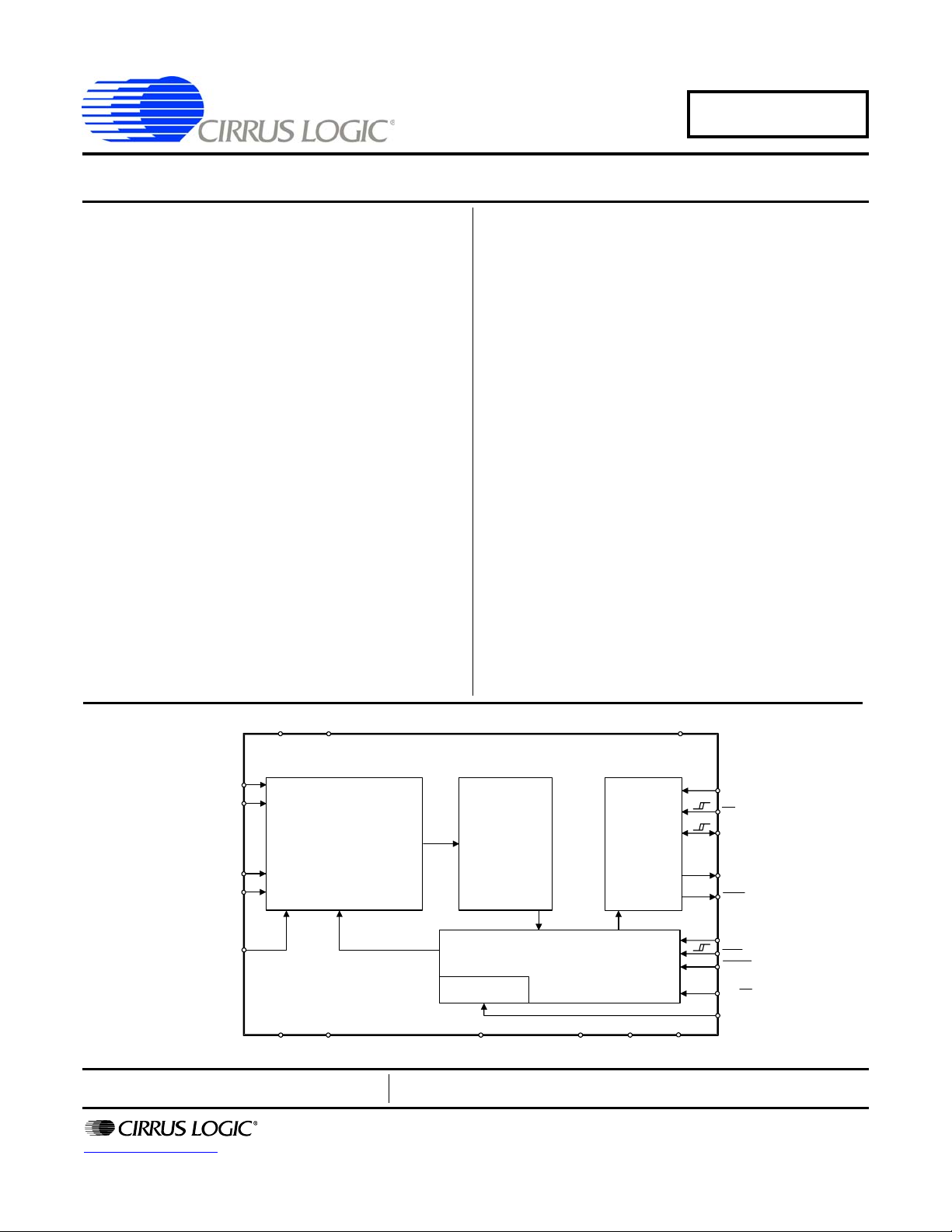
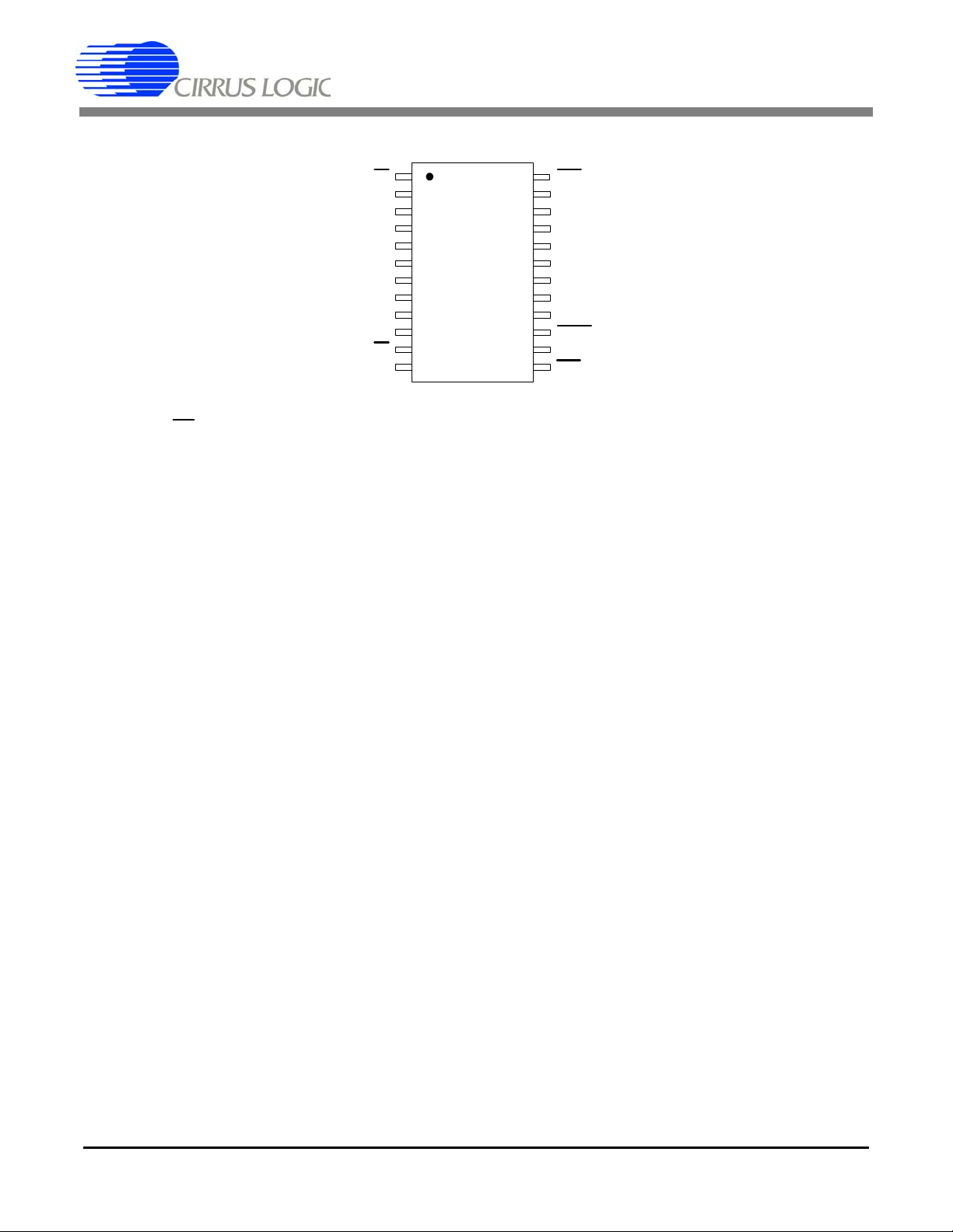
CS5571
∆Σ
ADC
V1+
VREF+
VREF-
AIN
ACOM
BUFEN
V1-
V2+
ADC
V2-
Preliminary Product Information
http://www.cirrus.com
VL
CS5571
SMODE
CS
DIGITAL
FILTER
LOGIC
OSC/CLOCK
GENERATOR
TST
This document contains information for a new product.
Cirrus Logic reserves the right to modify this product without notice.
Copyright © Cirrus Logic, Inc. 2008
(All Rights Reserved)
DIGITAL CONTROL
DCR
SERIAL
INTERFACE
VLR
VLR2
SCLK
SDO
RDY
DITHER
RST
CONV
BP/UP
MCLK
MAR ‘08
DS768PP1
Page 2

3/25/08
10:56
TABLE OF CONTENTS
1. CHARACTERISTICS AND SPECIFICATIONS . . . . . . . . . . . . . . . . . . . . . . . . . . . . . . . . . . . .4
ANALOG CHARACTERISTICS . . . . . . . . . . . . . . . . . . . . . . . . . . . . . . . . . . . . . . . . . . . . . . . .4
SWITCHING CHARACTERISTICS . . . . . . . . . . . . . . . . . . . . . . . . . . . . . . . . . . . . . . . . . . . . . 6
DIGITAL CHARACTERISTICS. . . . . . . . . . . . . . . . . . . . . . . . . . . . . . . . . . . . . . . . . . . . . . . .10
GUARANTEED LOGIC LEVELS . . . . . . . . . . . . . . . . . . . . . . . . . . . . . . . . . . . . . . . . . . . . . . 11
RECOMMENDED OPERATING CONDITIONS . . . . . . . . . . . . . . . . . . . . . . . . . . . . . . . . . . .12
ABSOLUTE MAXIMUM RATINGS . . . . . . . . . . . . . . . . . . . . . . . . . . . . . . . . . . . . . . . . . . . . . 12
2. OVERVIEW . . . . . . . . . . . . . . . . . . . . . . . . . . . . . . . . . . . . . . . . . . . . . . . . . . . . . . . . . . . . . . .13
3. THEORY OF OPERATION . . . . . . . . . . . . . . . . . . . . . . . . . . . . . . . . . . . . . . . . . . . . . . . . . . .13
3.1 Converter Operation . . . . . . . . . . . . . . . . . . . . . . . . . . . . . . . . . . . . . . . . . . . . . . . . . . . .13
3.2 Clock . . . . . . . . . . . . . . . . . . . . . . . . . . . . . . . . . . . . . . . . . . . . . . . . . . . . . . . . . . . . . . . . 14
3.3 Voltage Reference . . . . . . . . . . . . . . . . . . . . . . . . . . . . . . . . . . . . . . . . . . . . . . . . . . . . . .15
3.4 Analog Input . . . . . . . . . . . . . . . . . . . . . . . . . . . . . . . . . . . . . . . . . . . . . . . . . . . . . . . . . . . 15
3.5 Output Coding Format . . . . . . . . . . . . . . . . . . . . . . . . . . . . . . . . . . . . . . . . . . . . . . . . . . .16
3.6 Typical Connection Diagrams . . . . . . . . . . . . . . . . . . . . . . . . . . . . . . . . . . . . . . . . . . . . .17
3.7 AIN & VREF Sampling Structures . . . . . . . . . . . . . . . . . . . . . . . . . . . . . . . . . . . . . . . . . . 20
3.8 Converter Performance . . . . . . . . . . . . . . . . . . . . . . . . . . . . . . . . . . . . . . . . . . . . . . . . . . 20
3.9 DITHER . . . . . . . . . . . . . . . . . . . . . . . . . . . . . . . . . . . . . . . . . . . . . . . . . . . . . . . . . . . . . .24
3.10 Digital Filter Characteristics . . . . . . . . . . . . . . . . . . . . . . . . . . . . . . . . . . . . . . . . . . . . . .25
3.11 Serial Port . . . . . . . . . . . . . . . . . . . . . . . . . . . . . . . . . . . . . . . . . . . . . . . . . . . . . . . . . . .26
3.11.1 SSC Mode . . . . . . . . . . . . . . . . . . . . . . . . . . . . . . . . . . . . . . . . . . . . . . . . . . . . . 26
3.11.2 SEC Mode . . . . . . . . . . . . . . . . . . . . . . . . . . . . . . . . . . . . . . . . . . . . . . . . . . . . . 26
3.12 Power Supplies & Grounding . . . . . . . . . . . . . . . . . . . . . . . . . . . . . . . . . . . . . . . . . . . . .26
3.13 Using the CS5571 in Multiplexing Applications . . . . . . . . . . . . . . . . . . . . . . . . . . . . . . .27
3.14 Synchronizing Multiple Converters . . . . . . . . . . . . . . . . . . . . . . . . . . . . . . . . . . . . . . . .29
4. PIN DESCRIPTIONS . . . . . . . . . . . . . . . . . . . . . . . . . . . . . . . . . . . . . . . . . . . . . . . . . . . . . . .30
5. PACKAGE DIMENSIONS . . . . . . . . . . . . . . . . . . . . . . . . . . . . . . . . . . . . . . . . . . . . . . . . . . . . 33
6. ORDERING INFORMATION . . . . . . . . . . . . . . . . . . . . . . . . . . . . . . . . . . . . . . . . . . . . . . . . . 34
7. ENVIRONMENTAL, MANUFACTURING, & HANDLING INFORMATION . . . . . . . . . . . . . .34
8. REVISION HISTORY . . . . . . . . . . . . . . . . . . . . . . . . . . . . . . . . . . . . . . . . . . . . . . . . . . . . . . .34
CS5571
2 DS768PP1
Page 3

3/25/08
10:56
LIST OF FIGURES
Figure 1. SSC Mode - Read Timing, CS remaining low . . . . . . . . . . . . . . . . . . . . . . . . . . . . . . . . . 7
Figure 2. SSC Mode - Read Timing, CS falling after RDY falls . . . . . . . . . . . . . . . . . . . . . . . . . . . 8
Figure 3. SEC Mode - Continuous SCLK Read Timing . . . . . . . . . . . . . . . . . . . . . . . . . . . . . . . . . 9
Figure 4. SEC Mode - Discontinuous SCLK Read Timing . . . . . . . . . . . . . . . . . . . . . . . . . . . . . . 10
Figure 5. Voltage Reference Circuit . . . . . . . . . . . . . . . . . . . . . . . . . . . . . . . . . . . . . . . . . . . . . . .15
Figure 6. CS5571 Configured Using ±2.5V Analog Supplies . . . . . . . . . . . . . . . . . . . . . . . . . . . . 17
Figure 7. CS5571 Configured for Unipolar Measurement Using a Single 5V Analog Supply. . . . 18
Figure 8. CS5571 Configured for Bipolar Measurement Using a Single 5V Analog Supply. . . . . 19
Figure 9. CS5571 DNL Plot. . . . . . . . . . . . . . . . . . . . . . . . . . . . . . . . . . . . . . . . . . . . . . . . . . . . . . 20
Figure 10. CS5581 DNL Error Plot with DNL Histogram. . . . . . . . . . . . . . . . . . . . . . . . . . . . . . . . 20
Figure 11. Spectral Performance, 0 dB. . . . . . . . . . . . . . . . . . . . . . . . . . . . . . . . . . . . . . . . . . . . . 21
Figure 12. Spectral Performance, -6 dB . . . . . . . . . . . . . . . . . . . . . . . . . . . . . . . . . . . . . . . . . . . . 21
Figure 13. Spectral Performance, -12 dB . . . . . . . . . . . . . . . . . . . . . . . . . . . . . . . . . . . . . . . . . . . 21
Figure 14. Spectral Performance, -80 dB Dither On . . . . . . . . . . . . . . . . . . . . . . . . . . . . . . . . . . . 22
Figure 15. Spectral Performance, -80 dB Dither Off . . . . . . . . . . . . . . . . . . . . . . . . . . . . . . . . . . . 22
Figure 16. Spectral Performance, -100 dB Dither On. . . . . . . . . . . . . . . . . . . . . . . . . . . . . . . . . . 22
Figure 17. Spectral Performance, -100 dB Dither Off. . . . . . . . . . . . . . . . . . . . . . . . . . . . . . . . . . 22
Figure 18. Spectral Performance, -116.3 dB Dither On . . . . . . . . . . . . . . . . . . . . . . . . . . . . . . . . 23
Figure 19. Spectral Plot of Noise with Shorted Input . . . . . . . . . . . . . . . . . . . . . . . . . . . . . . . . . . 23
Figure 20. Noise Histogram, 4096 Samples Dither On, Code Center. . . . . . . . . . . . . . . . . . . . . . 24
Figure 21. Noise Histogram, 4096 Samples Dither Off, Code Center. . . . . . . . . . . . . . . . . . . . . . 24
Figure 22. Noise Histogram, 4096 Samples Dither On, Input at Code Boundary. . . . . . . . . . . . . 24
Figure 23. Noise Histogram, 4096 Samples Dither Off, Input at Code Boundary. . . . . . . . . . . . . 24
Figure 24. CS5571 Digital Filter Response (DC to fs/2) . . . . . . . . . . . . . . . . . . . . . . . . . . . . . . . . 25
Figure 25. CS5571 Digital Filter Response (DC to 10 kHz) . . . . . . . . . . . . . . . . . . . . . . . . . . . . . 25
Figure 26. CS5571 Digital Filter Response (DC to 4fs) . . . . . . . . . . . . . . . . . . . . . . . . . . . . . . . . 25
Figure 27. Simple Multiplexing Scheme . . . . . . . . . . . . . . . . . . . . . . . . . . . . . . . . . . . . . . . . . . . . 27
Figure 28. More Complex Multiplexing Scheme . . . . . . . . . . . . . . . . . . . . . . . . . . . . . . . . . . . . . . 28
CS5571
LIST OF TABLES
Table 1. Output Coding, Two’s Complement . . . . . . . . . . . . . . . . . . . . . . . . . . . . . . . . . . . . . . . . 16
Table 2. Output Coding, Offset Binary . . . . . . . . . . . . . . . . . . . . . . . . . . . . . . . . . . . . . . . . . . . . . 16
DS768PP1 3
Page 4
3/25/08
10:56
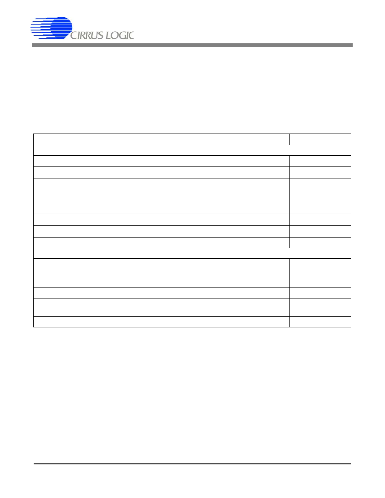
1. CHARACTERISTICS AND SPECIFICATIONS
• Min / Max characteristics and specifications are guaranteed over the specified operating conditions.
• Typical characteristics and specifications are measured at nominal supply voltages and T
• VLR = 0 V. All voltages measured with respect to 0 V.
A
CS5571
= 25°C.
ANALOG CHARACTERISTICS T
±5%; VL -VLR = 3.3 V, ±5%; VREF = (VREF+) - (VREF-) = 4.096V; MCLK = 16 MHz; SMODE = VL. DITHER = VL
unless otherwise stated; BUFEN = V1+ unless otherwise stated. Connected per Figure 6. Bipolar mode unless otherwise stated.
Parameter Min Typ Max Unit
Accuracy
Linearity Error - 0.0008 - ±%FS
Differential Linearity Error (Note 1) - - ±0.1 LSB
Positive Full-scale Error - 1.0 - %FS
Negative Full-scale Error - 1.0 - %FS
Full-scale Drift (Note 2, 3) - ±1 - LSB
Bipolar Offset (Note 2) - ±15 - LSB
Bipolar Offset Drift (Note 2, 3) - ±1 - LSB
Noise (Note 4) - 36 - µVrms
Dynamic Performance
Peak Harmonic or Spurious Noise 1 kHz, -0.5 dB Input
Total Harmonic Distortion 1 kHz, -0.5 dB Input - -94 -82 dB
Signal-to-Noise 91 92 - dB
= -40 to +85 °C; V1+ = V2+ = +2.5 V, ±5%; V1- = V2- = -2.5 V,
A
12 kHz, -0.5 dB Input--
-96
-96
-
-
dB
dB
16
16
16
16
S/(N + D) Ratio -0.5 dB Input, 1 kHz
-60 dB Input, 1 kHz--
-3 dB Input Bandwidth (Note 5) - 84 - kHz
1. No missing codes is guaranteed at 16 bits resolution over the specified temperature range.
2. One LSB is equivalent to VREF ÷ 2
3. Total drift over specified temperature range after reset at power-up, at 25º C.
4. With DITHER off the output will be dominated by quantization.
5. Scales with MCLK.
4 DS768PP1
16
or 4.096 ÷ 65536 = 62.5 µV.
91
32
-
-
dB
dB
Page 5
3/25/08
10:56
CS5571
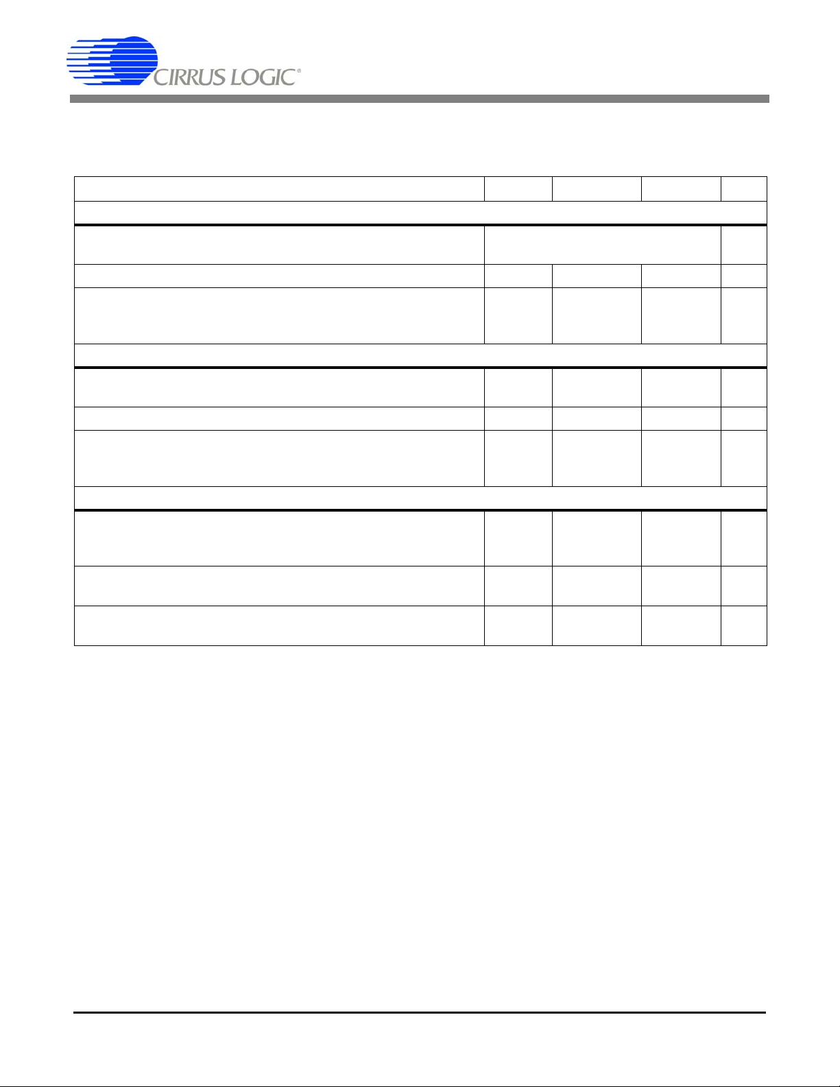
ANALOG CHARACTERISTICS (CONTINUED) T
V2- = -2.5 V, ±5%; VL -VLR = 3.3 V, ±5%; VREF = (VREF+) - (VREF-) = 4.096V; MCLK = 16 MHz; SMODE = VL.
DITHER = VL unless otherwise stated; BUFEN = V1+ unless otherwise stated. Connected per Figure 6.
Parameter Min Typ Max Unit
Analog Input
Analog Input Range Unipolar
Input Capacitance - 10 - pF
CVF Current (Note 6) AIN Buffer On (BUFEN = V+)
AIN Buffer Off (BUFEN = V-)
Voltage Reference Input
Voltage Reference Input Range
(VREF+) – (VREF-) (Note 7) 2.4 4.096
Input Capacitance - 10 - pF
CVF Current VREF+ Buffer On (BUFEN = V+)
VREF+ Buffer Off (BUFEN = V-)
Power Supplies
DC Power Supply Currents I
Power Consumption Normal Operation Buffers On
Power Supply Rejection (Note 8) V1+ , V2+ Supplies
V1-, V2- Supplies
= -40 to +85 °C; V1+ = V2+ = +2.5 V, ±5%; V1- =
A
0 to +VREF / 2
Bipolar
ACOM
VREF-
V1
I
V2
I
VL
Buffers Off
-
-
-
-
-
-
-
-
-
-
-
-
-
±VREF / 2
600
130
130
3
1
1
-
-
-
85
60
80
80
101
-
-
-
4.2
-
-
-
18
1.8
0.6
80
-
-
V
V
nA
µA
µA
V
µA
mA
mA
mA
mA
mA
mW
mW
dB
dB
6. Measured using an input signal of 1 V DC.
7. For optimum performance, VREF+ should always be less than (V+) - 0.2 volts to prevent saturation of the VREF+ input buffer.
8. Tested with 100 mVp-p on any supply up to 1 kHz. V1+ and V2+ supplies at the same voltage potential, V1- and V2- supplies at
the same voltage potential.
DS768PP1 5
Page 6
3/25/08
10:56
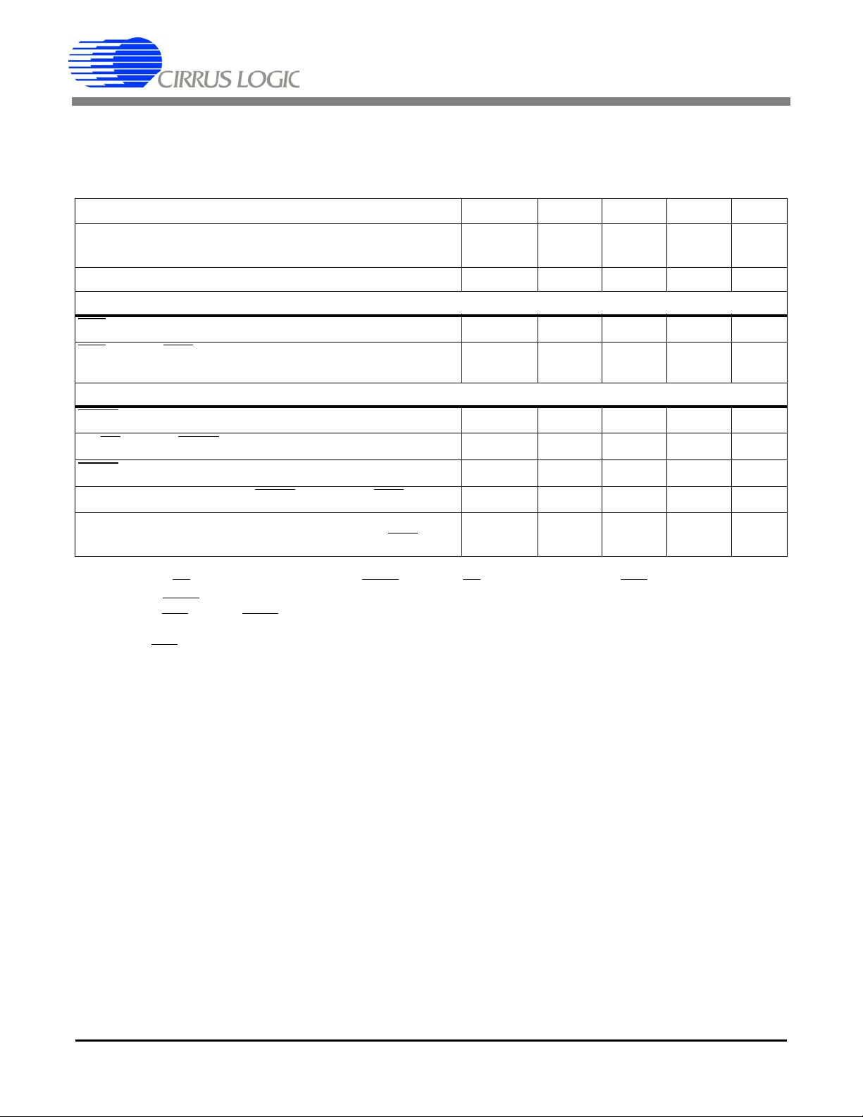
SWITCHING CHARACTERISTICS
TA= -40 to +85 °C; V1+ = V2+ = +2.5 V, ±5%; V1- = V2- = -2.5 V, ±5%;
VL - VLR = 3.3 V, ±5%, 2.5 V, ±5%, or 1.8 V, ±5%
Input levels: Logic 0 = 0V = Low; Logic 1 = VD+ = High; CL = 15 pF.
Parameter Symbol Min Typ Max Unit
CS5571
Master Clock Frequency Internal Oscillator
External Clock
Master Clock Duty Cycle 40 - 60 %
Reset
RST
Low Time (Note 9) t
rising to RDY falling Internal Oscillator
RST
External Clock
Conversion
CONV
Pulse Width t
setup to CONV falling (Note 10) t
BP/UP
low to start of conversion t
CONV
Perform Single Conversion (CONV
Conversion Time (Note 11)
Start of Conversion to RDY
9. Reset must not be released until the power supplies and the voltage reference are within specification.
10. BP/UP
11. If CO NV is held low contin uously, conversions occur every 160 MCLK cycles.
can be changed coincident to CONV falling. BP/UP must remain stable until RDY falls.
is tied to CONV, conversions will occur every 162 MCLKs.
If RDY
If CONV is operated asynchronously to MCLK, a conversion may take up to 164 MCLKs.
RDY falls at the end of conversion.
high before RDY falling) t
falling t
XIN
f
clk
res
t
wup
cpw
scn
scn
bus
buh
12
0.5
1--µs
-
-
4--MCLKs
0--ns
--2MCLKs
20 - - MCLKs
--164MCLKs
14
16
120
1536
16
16.2
-
-
MHz
MHz
µs
MCLKs
6 DS768PP1
Page 7
3/25/08
10:56
SWITCHING CHARACTERISTICS (CONTINUED)
TA= -40 to +85 °C; V1+ = V2+ = +2.5 V, ±5%; V1- = V2- = -2.5 V, ±5%;
VL - VLR = 3.3 V, ±5%, 2.5 V, ±5%, or 1.8 V, ±5%
Input levels: Logic 0 = 0V = Low; Logic 1 = VD+ = High; CL = 15 pF.
Parameter Symbol Min Typ Max Unit
Serial Port Timing in SSC Mode (SMODE = VL)
RDY
falling to MSB stable t
Data hold time after SCLK rising t
Serial Clock (Out) Pulse Width (low)
(Note 12, 13) Pulse Width (high)
rising after last SCLK rising t
RDY
12. SDO and SCLK will be high impedance when CS is high. In some systems SCLK and SDO may require pull-down
resistors.
13. SCLK = MCLK/2.
1
2
t
3
t
4
5
CS5571
--2-MCLKs
-10-ns
50
50
-8-MCLKs
-
-
-
-
ns
ns
MCLK
RDY
SCLK(o)
SDO
CS
t
1
t
2
MSB MSB–1
t
3
t
4
LSB
LSB+1
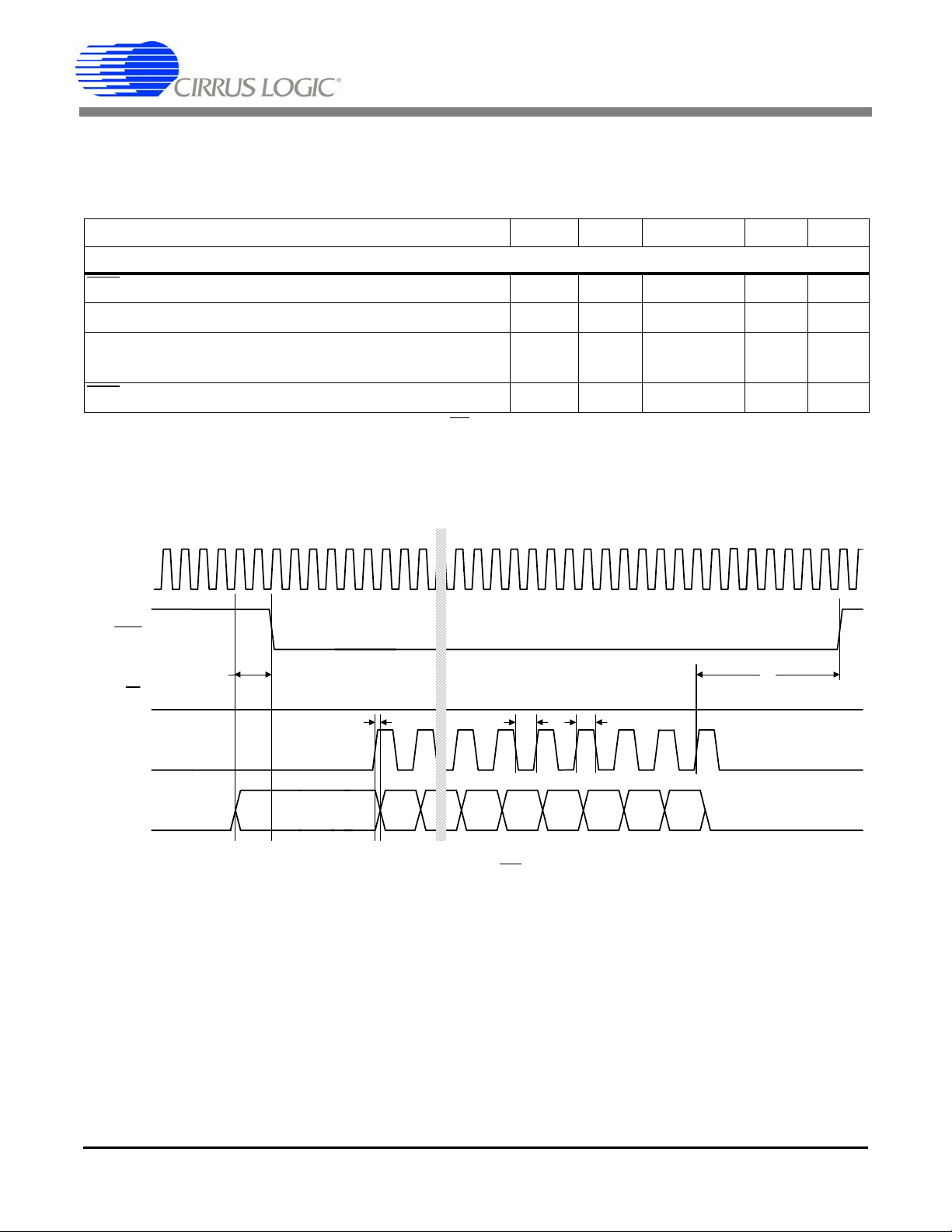
Figure 1. SSC Mode - Read Timing, CS remaining low (Not to Scale)
t
5
DS768PP1 7
Page 8
3/25/08
10:56
SWITCHING CHARACTERISTICS (CONTINUED)
TA= -40 to +85 °C; V1+ = V2+ = +2.5 V, ±5%; V1- = V2- = -2.5 V, ±5%;
VL - VLR = 3.3 V, ±5%, 2.5 V, ±5%, or 1.8 V, ±5%
Input levels: Logic 0 = 0V = Low; Logic 1 = VD+ = High; CL = 15 pF.
Parameter Symbol Min Typ Max Unit
Serial Port Timing in SSC Mode (SMODE = VL)
Data hold time after SCLK rising t
Serial Clock (Out) Pulse Width (low)
(Note 14, 15) Pulse Width (high)
RDY
rising after last SCLK rising t
falling to MSB stable t
CS
First SCLK rising after CS
hold time (low) after SCLK rising t
CS
SCLK, SDO tri-state after CS
14. SDO and SCLK will be high impedance when CS is high. In some systems SCLK and SDO may require pull-down
resistors.
15. SCLK = MCLK/2.
falling t
rising t
t
t
10
11
12
13
14
7
8
9
CS5571
-10-ns
50
50
-8-MCLKs
-10-ns
-8-MCLKs
10 - - ns
-5-ns
-
-
-
-
ns
ns
MCLK
RDY
SCLK(o)
SDO
CS
t
13
t
12
t
11
MSB MSB–1
t
7
t
8
t
9
LSB+1
LSB
t
14
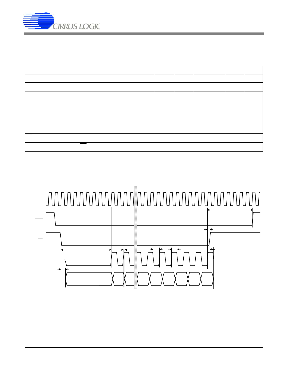
Figure 2. SSC Mode - Read Timing, CS falling after RDY falls (Not to Scale)
t
10
8 DS768PP1
Page 9
3/25/08
10:56
SWITCHING CHARACTERISTICS (CONTINUED)
TA= -40 to +85 °C; V1+ = V2+ = +2.5 V, ±5%; V1- = V2- = -2.5 V, ±5%;
VL - VLR = 3.3 V, ±5%, 2.5 V, ±5%, or 1.8 V, ±5%
Input levels: Logic 0 = 0V = Low; Logic 1 = VD+ = High; CL = 15 pF.
Parameter Symbol Min Typ Max Unit
Serial Port Timing in SEC Mode (SMODE = VLR)
SCLK(in) Pulse Width (High)
SCLK(in) Pulse Width (Low)
CS
hold time (high) after RDY falling t
hold time (high) after SCLK rising t
CS
CS
low to SDO out of Hi-Z (Note 16) t
Data hold time after SCLK rising t
Data setup time before SCLK rising t
CS
hold time (low) after SCLK rising
-
-
15
16
17
18
19
t
20
CS5571
30 - - ns
30 - - ns
10 - - ns
10 - - ns
-10-ns
-10-ns
10 - - ns
1
10 - ns
SCLK
10
RDY
rising after SCLK falling t
16. SDO will be high impedance when CS is high. In some systems SDO may require a pull-down resistor.
MCLK
RDY
t
15
CS
t
16
SCLK(i)
t
17
t
t
19
18
SDO
21
-10-ns
t
21
t
20
LSBMSB
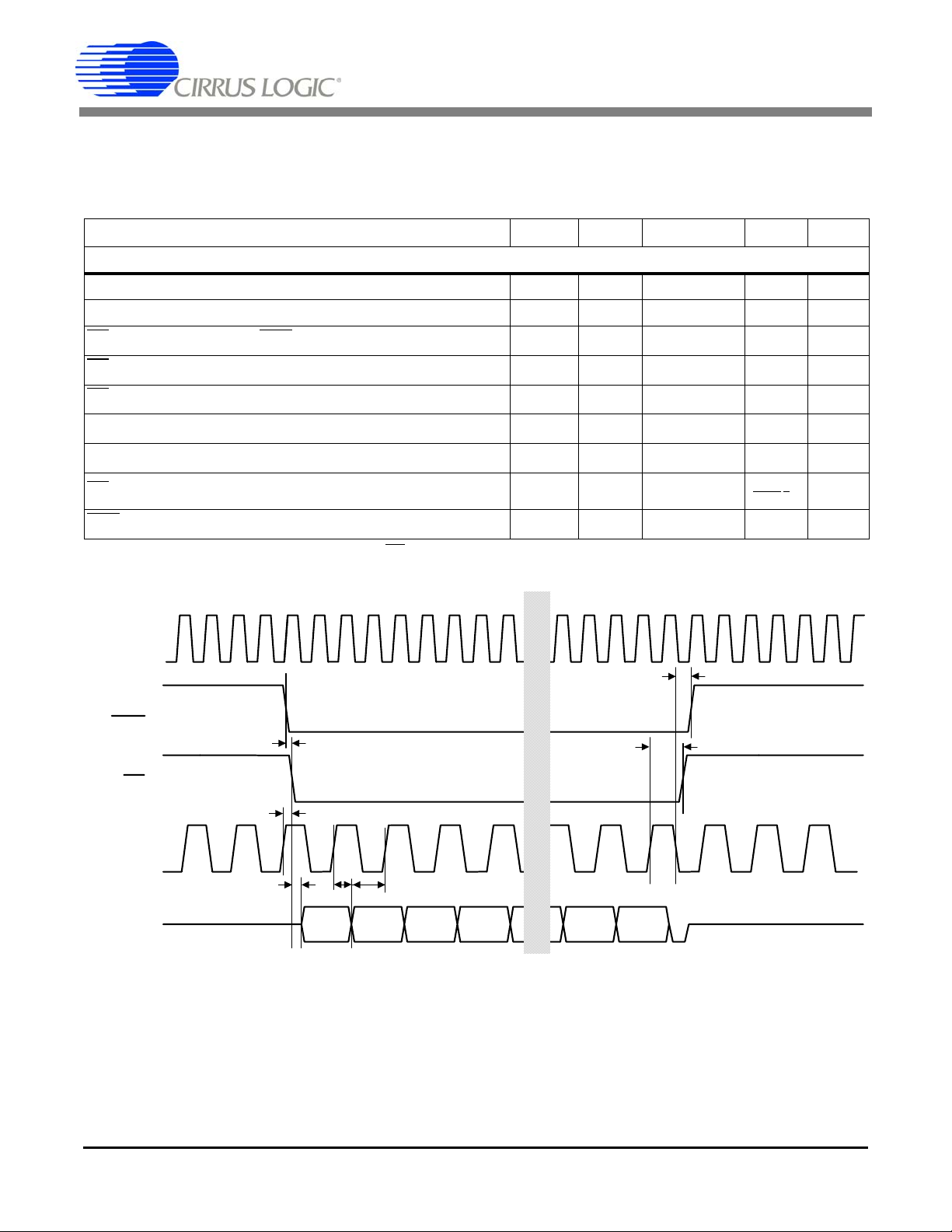
Figure 3. SEC Mode - Continuous SCLK Read Timing (Not to Scale)
DS768PP1 9
Page 10
MCLK
RDY
SCLK(i)
SDO
CS
3/25/08
10:56
t
21
t
15
t
17
t
t
19
18
t
20
LSBMSB
CS5571
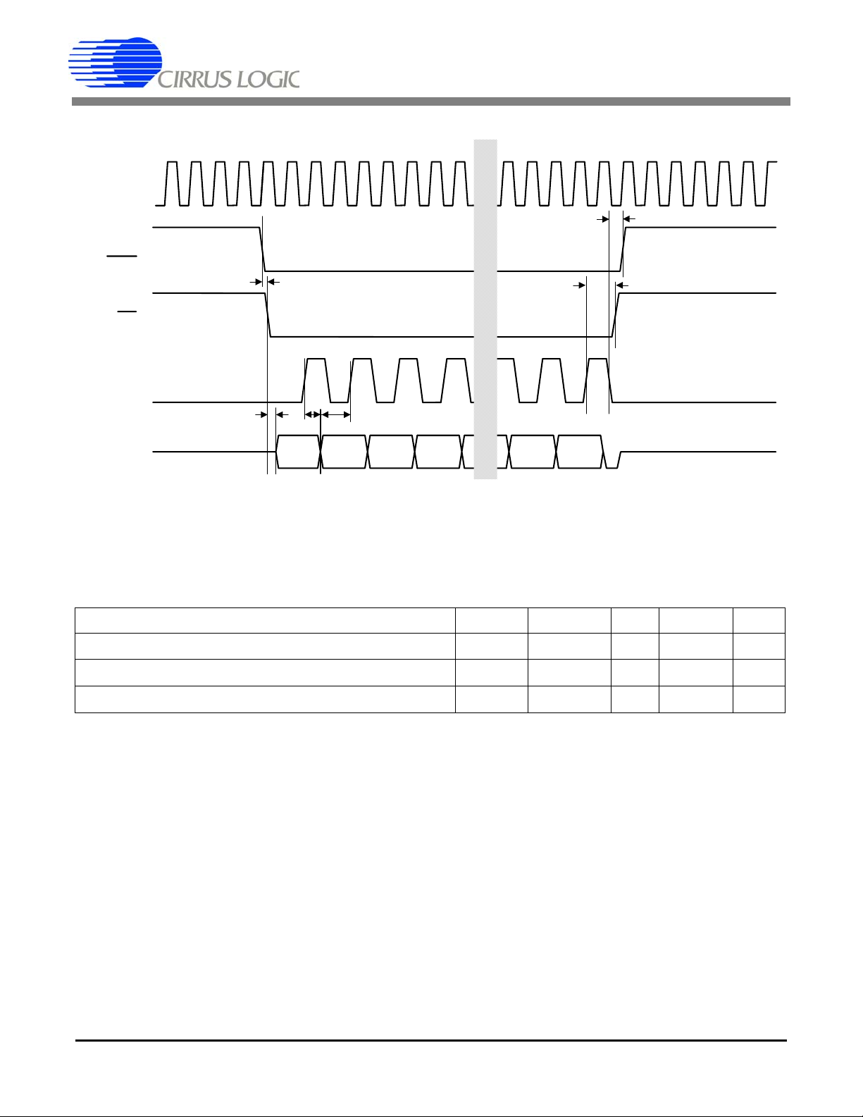
Figure 4. SEC Mode - Discontinuous SCLK Read Timing (Not to Scale)
DIGITAL CHARACTERISTICS
= TMIN to TMAX; VL = 3.3V, ±5% or VL = 2.5V, ±5% or 1.8V, ±5%; VLR = 0V
T
A
Parameter Symbol Min Typ Max Unit
Input Leakage Current I
Digital Input Pin Capacitance C
Digital Output Pin Capacitance C
in
in
out
--2µA
-3-pF
-3-pF
10 DS768PP1
Page 11
3/25/08
10:56
GUARANTEED LOGIC LEVELS
TA=-40to+85°C;V1+=V2+=+2.5V, ±5%; V1- = V2- = -2.5 V, ±5%;
VL - VLR = 3.3 V, ±5%, 2.5 V, ±5%, or 1.8 V, ±5%
Input levels: Logic 0 = 0V = Low; Logic 1 = VD+ = High; CL = 15 pF.
Guaranteed Limits
Parameter Sym VL Min Typ Max Unit Conditions
Logic Inputs
3.3 1.9
Minimum High-level Input Voltage:
Maximum Low-level Input Voltage:
Logic Outputs
Minimum High-level Output Voltage:
Maximum Low-level Output Voltage:
V
IH
1.8 1.2
3.3 1.1
V
IL
1.8 0.6
3.3 2.9
V
OH
V
OL
2.5 2.1
1.8 1.65
3.3 0.36
2.5 0.36
1.8 0.44
CS5571
V2.5 1.6
V2.5 0.95
V
V
IOH=-2mA
IOH=-2mA
DS768PP1 11
Page 12

3/25/08
10:56
RECOMMENDED OPERATING CONDITIONS
(VLR = 0V, see Note 17)
Parameter Symbol Min Typ Max Unit
Single Analog Supply
DC Power Supplies: (Note 17)
V1+
V2+
V1V2-
Dual Analog Supplies
DC Power Supplies: (Note 17)
V1+
V2+
V1V2-
V1+
V2-
V1+
V2-
V1+
V2-
V1+
V2-
4.75
4.75
-
-
+2.375
+2.375
-2.375
-2.375
5.0
5.0
0
0
+2.5
+2.5
-2.5
-2.5
CS5571
5.25
5.25
-
-
+2.625
+2.625
-2.625
-2.625
V
V
V
V
V
V
V
V
Analog Reference Voltage (Note 18)
[VREF+] – [VREF-]
17. The logic supply can be any value VL – VLR = +1.71 to +3.465 volts as long as VLR ≥ V2- and VL ≤ 3.465 V.
18. The differential voltage reference magnitude is constrain ed by the V1+ or V1- supply magnitude.
ABSOLUTE MAXIMUM RATINGS
(VLR = 0V)
Parameter Symbol Min Typ Max Unit
DC Power Supplies:
[V1+] – [V1-] (Note 19)
VL + [ |V1-| ] (Note 20)
Input Current, Any Pin Except Supplies (Note 21) I
Analog Input Voltage (AIN and VREF pins) V
Digital Input Voltage V
Storage Temperature T
Notes:
19. V1+ = V2+; V1- = V2-
20. V1- = V2-
21. Transient currents of up to 100 mA wi ll not cause SCR latch-up.
VREF 2.4 4.096 4.2 V
-
-
IN
INA
IND
stg
0
0
--±10mA
(V1-) – 0.3 - (V1+) + 0.3 V
VLR – 0.3 - VL + 0.3 V
-65 - 150 °C
-
-
5.5
6.1
V
V
WARNING:
Recommended Operating Conditions indicate limits to which the device is functionally ope rational. Absolute Maximum Ratings indicate limits beyond which permanent damage to the device may occur. The
Absolute Maximum Ratings are stress ratings only and the device should not be operated at these limits.
Operation at conditions beyond the Recommended Operating Conditions may affect device reliability, and
functional operation beyond Recommended Operating Conditions is not implied. Performance specifications are intended for the conditions specified for each table in the Characteristics and Specifications section.
12 DS768PP1
Page 13

3/25/08
10:56
2. OVERVIEW
The CS5571 is a 16-bit analog-to-digital converter capable of 100 kSps conversion rate. The analog inp ut
accepts a single-ended input with a magnitude of ±VREF / 2
tiple input channels at a high rate with no loss in throughput. The ADC uses a low-latency digital filter architecture. The filter is designed for fast settling and settles to full accuracy in one conversion.
The converter is a serial output device. The serial port can be configured to funct ion as either a master or
a slave.
The converter can operate from an analog supply of 5V or from ±2.5V. The digital interface supports standard logic operating from 1.8, 2.5, or 3.3 V.
The CS5571 may convert at rates up to 100 kSps when operating from a 16 MHz input clock.
3. THEORY OF OPERATION
The CS5571 converter provides high-performance measurement of DC or AC signals. The converter can
be used to perform single conversions or continuous conversions upon command. Each conversion is independent of previous conversions and settles to full specified accuracy, even with a full-scale input voltage step. This is due to the converter architecture which uses a combination of a high-spe ed delta-sigma
modulator and a low-latency filter architecture.
volts. The device is capable of switching mul-
CS5571
Once power is established to the converter, a reset must be performed. A reset initializes the internal converter logic.
If CONV
equivalent to 100 kSps if MCLK = 16.0 MHz. If CONV
MCLKs. If CONV
to RDY
Multiple converters can operate synchronously if they are driven by the same MCLK source and CONV
to each converter falls on the same MCLK falling edge. Alternately, CONV can be h eld low and all devices
can be synchronized if they are reset with RST
The output coding of the conversion word is a function of the BP/UP
is held low, the converter will convert continuously with RDY falling every 160 MCLKs. This is
is tied to RDY, a conversion will occur every 162
is operated asynchronously to MCLK, it may take up to 164 MCLKs from CONV falling
falling.
rising on the same falling edge of MCLK.
pin.
3.1 Converter Operation
The converter should be reset after the power supplies and voltage reference are stable.
The CS5571 converts at 100 kSps when synchronously operated (CONV
clock. Conversion is initiated by taking CONV
CONV
when a conversion actually begins. This may extend the throughput to 164 MCLKs per conversion.
When the conversion is completed, the output word is placed into the serial port and RDY
convert continuously, CONV
conversion is performed in 160 MCLK cycles. Alternately RDY
occur every 162 MCLK cycles.
is asynchronous to MCLK there may be an uncertainty of 0-4 MCLK cycles after CONV falls to
should be held low. In continuous conversion mode with CONV held low, a
low. A conversion lasts 160 master clock cycles, but if
can be tied to CONV and a conversion will
= VLR) from a 16.0 MHz master
goes low. To
To perform only one conversion, CONV
falls.
DS768PP1 13
should return high at least 20 master clock cycles before RDY
Page 14

3/25/08
10:56
Once a conversion is completed and RDY falls, RDY will return high when all the bits of the data word are
emptied from the serial port or if the conversion data is not read and CS
MCLK cycles before the end of conversion. RDY
is put into the port register.
See Serial Port on page 26 for information about reading conversion data.
Conversion performance can be affected by several factors. These include the choice of clock so urce for
the chip, the timing of CONV
The converter can be operated from an internal oscillator. This clock source has greater jitter than an
external crystal-based clo ck. Jitter may not be an issue when measuring DC signals, or very-low-frequency AC signals, but can become an issue for higher frequency AC signals. For maximum performance
when digitizing AC signals, a low-jitter MCLK should be used.
To achieve the highest resolution when measuring a DC signal with a single conversion the DITHER function should be off. If averaging is to be performed with multiple conversions of a DC signal, DITHER
should be on. To maximize performance, the CONV
state to perform multiple conversions, or CONV
falls.
, the setting of the DITHER function, and the choice of the serial port mode.
will fall at the end of the next conversion when new data
pin should be held low in the continuous conversion
should occur synchronous to MCLK, falling when MCLK
is held low, RDY will go high two
CS5571
If the converter is operated at maximum throughput, the SSC serial port mode is less likely to cause interference to measurements as the SCLK output is synchronized to the MCLK. Alternately, any interference due to serial port clocking can also be minimized if data is read in the SEC serial port mode when a
conversion is not in progress.
3.2 Clock
The CS5571 can be operated from its internal oscillator or from an external master clock. The state of
MCLK determines which clock source will be used. If MCLK is tied low, the internal oscillator will start and
be used as the clock source for the converter. If an external CMOS-compatible clock is input into MCLK,
the converter will power down the internal oscillator and use the external clock. If the MCLK pin is held
high, the internal oscillator will be held in the stopped state. The MCLK input can be held high to delete
clock cycles to aid in synchronizing multiple converters in different phase relationships.
The internal oscillator can be used if the signals to be measured are essentially DC. The internal oscillator
exhibits jitter at about 500 picoseconds rms. If the CS5571 is used to digitize AC signals, an external
low-jitter clock source should be used.
If the internal oscillator is used as the clock for the CS5571, the maximum conversion rate will be dictated
by the oscillator frequency.
If driven from an external MCLK source, the fast rise and fall times of the MCLK signal can result in clock
coupling from the internal bond wire of the IC to the analog input. Adding a 50 ohm resistor on the external
MCLK source significantly reduces this effect.
14 DS768PP1
Page 15
3/25/08
10:56
3.3 Voltage Reference
The voltage reference for the CS5571 can range from 2.4 volt to 4.2 volts. A 4.096 volt reference is required to achieve the specified signal-to-noise performance. Figure 6 and Figure 7 illustrate the connec-
tion of the voltage reference with either a single +5 V analog supply or with ±2.5 V.
For optimum performance, the voltage reference device should be one that provides a capacitor connection to provide a means of noise filtering, or the output should include some type of bandwidth-limiting filter.
Some 4.096 volt reference devices need only 5 volts total supply for operation and can be connected as
shown in Figure 6 or Figure 7. The reference should have a local bypass capacitor and an appropriate
output capacitor.
Some older 4.096 voltage reference designs require more headroom and must operate from an input voltage of 5.5 to 6.5 volts. If this type of voltage reference is used ensure that when power is applied to the
system, the voltage reference rise time is slower than the rise time of the V1 + and V1- power sup ply voltage to the converter. An example circuit to slow the output startup time of the reference is illustrated in
Figure 5.
5.5 t o 15 V
CS5571
2k
10µF
VIN
VOUT
GND
Figure 5. Voltage Reference Circuit
4. 096 V
Refer to V1-and VREF1 pins.
3.4 Analog Input
The analog input of the converter is single-ended with a full-scale input of ±2.048 volts, relative to the
ACOM pin.. This is illustrated in Figure 6 and Figure 7. These diagrams also illustrate a differential buffer
amplifier configuration for driving the CS5571.
The capacitors at the outputs of the amplifiers provide a charge reservoir for the dynamic current from t he
A/D inputs while the resistors isolate the dynamic current from the amplifier. The amplifiers can be powered from higher supplies than those used by the A/D but precautions should be taken to ensure that t he
op-amp output voltage remains within the power supply limits of the A/D, especially under start-up conditions.
DS768PP1 15
Page 16

3/25/08
10:56
3.5 Output Coding Format
The reference voltage directly defines the input voltage range in both the unipolar and bipolar configurations. In the unipolar configuration (BP/UP
the final code transition occurs 1.5 LSBs below VREF. In the bipolar configuration (BP/UP
code transition occurs 0.5 LSB above -VREF and the last transition occurs 1.5 LSBs below +VREF. See
Table 1 for the output coding of the converter.
Table 1. Output Coding, Two’s Complement
low), the first code transition occurs 0.5 LSB above zero, and
CS5571
high), the first
Bipolar Input Voltage
NOTE: VREF = [(VREF+) - (VREF-)] / 2
Table 2. Output Coding, Offset Binary
Unipolar Input Voltage
Two’s
Complement
>(VREF-1.5 LSB) 7F FF
7F FF
VREF-1.5 LSB
7F FE
00 00
-0.5 LSB
FF FF
80 01
-VREF+0.5 LSB
80 00
<(-VREF+0.5 LSB) 80 00
Offset
Binary
>(VREF-1.5 LSB) FF FF
FF FF
VREF-1.5 LSB
FF FE
80 00
(VREF/2)-0.5 LSB
7F FF
00 01
+0.5 LSB
00 00
<(+0.5 LSB) 00 00
NOTE: VREF = [(VREF+) - (VREF-)] / 2
16 DS768PP1
Page 17

3/25/08
10:56
3.6 Typical Connection Diagrams
The following figure depicts the CS5571 powered from bipolar analog supplies, +2.5 V and - 2.5 V.
+2.048 V
0 V
-2.048 V
CS5571
CS5571
+2.5 V
+4.096
Voltage
Reference
(NOTE 1)
-2.5 V
49.9
150pF
2k
(V+) Buffers On
10 µF0.1 µF
4700pF
(V-) Buffers Off
C0G
ACOM
BUFEN
+2.5 V
AIN
VREF+
VREF-
SMODE
CS
5
SCLK
5
SDO
RDY
CONV
BP/UP
DITHER
RST
MCLK
TST
+3.3 V to +1.8 V
50
V1+
10
0.1 µF
0.1 µF
10
0.1 µF
X7R
-2.5 V
NOTES
1. See Section 3.3 Voltage Reference for informat ion on required
voltage reference performance criteria.
2.Locate capacitors so as to minimize loop length.
3. The ±2.5 V supplies should also be bypass ed to ground at the converter.
4. VLR and the power supply ground for the ±2.5 V should be
connected to the same ground plane under the chip.
5. SCLK and SDO may require pull-down resistors in some applications.
V2+
V2-
DCR
V1-
VL
0.1 µF
VLR2
VLR
Figure 6. CS5571 Configured Using ±2.5V Analog Supplies
DS768PP1 17
Page 18
3/25/08
10:56
The following figure depicts the CS5571 part powered from a single 5V analog supply and configu red for
unipolar measurement.
0 V to +2.048 V
CS5571
CS5571
CS3003 / CS3004
+5 V
+4.096
Voltage
Reference
(NOTE 1)
49.9
150pF
2k
(V+) Buffers On
(V-) Buffers Off
4700pF
C0G
0.1 µF10 µF
AIN
ACOM
BUFEN
VREF+
VREF-
+5 V
SMODE
CS
4
SCLK
4
SDO
RDY
CONV
BP/UP
DITHER
RST
MCLK
TST
+3.3 V to 1.8 V
50
V1+
0.1 µF
10
V2+
0.1 µF
0.1 µF
X7R
NOTES
1. See Section 3.3 Voltage Reference for information on
required voltage reference performance criteria.
2. Locate capacitors so as to mini mize loop length.
3. V1-, V2-, and VLR should be connected to the sa me
ground plane under the chip.
4. SCLK and SDO may require pull-down resistors in
some applications.
V2-
DCR
V1-
VL
0.1 µF
VLR2
VLR
Figure 7. CS5571 Configured for Unipolar Measurement Using a Single 5V Analog Supply
18 DS768PP1
Page 19

3/25/08
10:56
The following figure depicts the CS5571 part powered from a single 5V analog supply and configu red for
bipolar measurement, referenced to a common mode voltage of 2.5 V.
+4.548 V
+2.5 V
+0.452 V
CS5571
Common Mode Voltage
(2.5 V Typ.)
CS3003 / CS3004
CS3003 / CS3004
+5 V
+4.096
Voltage
Reference
(NOTE 1)
49.9
150pF
2k
49.9
150pF
2k
(V+) Buffers On
(V-) Buffers Off
4700pF
C0G
4700pF
C0G
0.1 µF10 µF
AIN
ACOM
BUFEN
VREF+
VREF-
+5 V
CS5571
SMODE
CS
4
SCLK
4
SDO
RDY
CONV
CAL
BP/UP
DITHER
RST
MCLK
TST
+3.3 V to 1.8 V
50
V1+
10
0.1 µF
0.1 µF
0.1 µF
X7R
NOTES
1. See Section 3.3 Voltage Reference for information on
required voltage reference performance criteria.
2. Locate capacitors so as to minimize loop length.
3. V1-, V2-, and VLR should be connected to the same
ground plane under the chip.
4. SCLK and SDO may require pull-down resistors in
some applications.
V2+
V2-
DCR
V1-
VL
0.1 µF
VLR2
VLR
Figure 8. CS5571 Configured for Bipolar Measurement Using a Single 5V Analog Supply
DS768PP1 19
Page 20

3/25/08
10:56
3.7 AIN & VREF Sampling Structures
The CS5571 uses on-chip buffers on the AIN and VREF+ inputs. Buffers provide much higher input impedance and therefore reduce the amount of drive current required from an external source. This helps
minimize errors.
The Buffer Enable (BUFEN) pin determines if the on-chip buffers are used or not. If the BUFEN pin is
connected to the V1+ supply, the buffers will be enabled. If the BUFEN pin is connected to the V1- pin,
the buffers are off. The converter will consume about 30 mW less power when the buffers are off, but the
input impedances of AIN, ACOM and VREF+ will be significantly less than with the buffers enabled.
3.8 Converter Performance
The CS5571 achieves excellent differential nonlinearity (DNL) as shown in figures 9 and 10. Figure 9 illustrates the code widths on a typical scale of ±1 LSB. Figure 10 illustrates a zoom view of figure 9 on a
scale of ±0.1 LSB. Figure 10 also includes a DNL error histogram that indicates that the errors are equally
distributed about the perfect code size; and most codes are accurate within ±0.01 LSB.
1.00
0.75
0.50
0.25
0.00
-0.25
-0.50
DNL Error in LSBs
-0.75
-1.00
1 65535
Figure 9. CS5571 DNL Plot
Codes
CS5571
+0.10
+0.08
+0.06
+0.04
+0.02
0
-0.02
DNL Error in LSBs
-0.04
-0.06
-0.08
-0.10
1 65535
Codes
18k
16k
14k
12k
10k
8k
Counts per 0.01 LSB Error
4k
6k
+0.1
+0.09
+0.08
+0.07
+0.06
+0.05
+0.04
+0.03
+0.02
+0.01
0
-0.01
-0.02
DNL Error in LSBs
-0.03
-0.04
-0.05
-0.06
-0.07
-0.08
-0.09
-0.1
0
2k
Figure 10. CS5581 DNL Error Plot with DNL Histogram
20 DS768PP1
Page 21

3/25/08
k
k
k
10:56
Figures 11, 12, and 13 indicate the spectral performance of the CS5571 with a 0 dB, -6 dB and - 12 dB
5.55 kHz input signal. In each case, the captured data was windowed with a seven-term window function
that exhibits 4.3 dB of attenuation before being processed by the FFT.
CS5571
0
-20
-40
-60
-80
-100
-120
-140
-160
0 10k 20k 30k 40k 50
Frequency (Hz)
5.55 kHz, 0 dB
32k Samples @ 100 kSps
0
-20
-40
-60
-80
-100
-120
-140
-160
0 10k 20k 30k 40k 50
Frequency (Hz)
5.55 kHz, -6 dB
32k Samples @ 100 kSps
Figure 11. Spectral Performance, 0 dB Figure 12. Spectral Performance, -6 dB
0
-20
-40
-60
-80
-100
-120
-140
-160
0 10k 20k 30k 40k 50
Frequency (Hz)
5.55 kHz, -12 dB
32k Samples @ 100 kSps
Figure 13. Spectral Performance, -12 dB
DS768PP1 21
Page 22

3/25/08
k
k
k
k
10:56
Figures 14 and 15 illustrate the small signal performance of the CS5571 with a 5.55 kHz signal at -80 dB
down. Figure 14 is with DITHER on and Figure 15 is with DITHER off. At -80 dB the signal is 1/10,000
of full scale, having a peak-to-peak magnitude of only a few codes. For small signals, DNL errors and
quantization errors can introduce distortion because the error in the code size, or the quantization error
without adequate dither, are a much greater percentage of the signal than with a full-scale input. Figure
15, with DITHER off, illustrates that distortion components can be introduced when there is not adequa te
dither to randomize the quantization error.
CS5571
0
-20
-40
-60
-80
-100
-120
-140
-160
0 10k 20k 30k 40k 50
Frequency (Hz)
5.55 kHz, -80 dB
32k Samples @ 100 kSps
Dither On
Figure 14. Spectral Performance, -80 dB
Dither On
0
-20
-40
-60
-80
-100
-120
-140
-160
0 10k 20k 30k 40k 50
Frequency (Hz)
Figure 15. Spectral Performance, -80 dB
Dither Off
Figures 16 and 17 illustrate DITHER on and DITHER off with a 5.55 kHz input at -100 dB. At -100 dB the
signal is only about 41 microvolts peak to peak. This is less than the one code width which is about
62.5 microvolts.
0
-20
-40
-60
-80
-100
-120
-140
-160
0 10k 20k 30k 40k 50
Frequency (Hz)
0
-20
-40
-60
-80
-100
-120
-140
-160
0 10k 20k 30k 40k 50
Frequency (Hz)
Figure 16. Spectral Performance, -100 dB
Dither On
Figure 17. Spectral Performance, -100 dB
Dither Off
22 DS768PP1
Page 23

3/25/08
k
k
10:56
Figure 18 illustrates a test signal of 5.55 kHz, 116.3 dB down, which is only 6.3 microvolts peak to peak,
or about 1/10 of a code width. The converter can reliably digitize this signal because of its excellent DNL
and proper dither.
0
-20
-40
-60
-80
-100
-120
-140
-160
0 10k 20k 30k 40k 50
Frequency (Hz)
Figure 18. Spectral Performance, -116.3 dB
Dither On
Figure 19 is a spectral plot of the converter with its input grounded. The spectral information is on a logarithmic frequency axis as this illustrates the very low frequency behavior of the converter. Fig ure 19 was
produced from averaging the results of 16 FFT outputs using 2 million samples each. This plot also illustrates that the converter noise floor is free of spurious components that may be present in other converters
due to on-chip digital interference.
CS5571
0
-20
-40
-60
-80
-100
-120
-140
-160
-180
0.1 1 10 100 1k 10k
Frequency (Hz)
Shorted Input
2M Samples @ 100 kSps
16 Averages
Figure 19. Spectral Plot of Noise with Shorted Input
50
DS768PP1 23
Page 24

3/25/08
10:56
Figure 20 illustrates a noise histogram of 4096 samples with the input signal adjusted to almost the exact
center of a code with DITHER on. Figure 21 illustrates a noise histogram of 4096 samples with the input
signal at the center of a code with DITHER off.
Notice that with a signal at the center of a code that the converter outputs the same code over 96 % of the
time. Figures 22 and 23 illustrate the noise histogram, DITHER on and then DITHER off with the input
signal at a code boundary. Notice that in the DITHER off case the converter only exhibits two codes of
noise.
CS5571
4500
4000
3500
3000
2500
2000
1500
1000
500
3
0
-2 -1 0
2624
Output (Codes)
Output (Codes)
751709
12
Figure 20. Noise Histogram, 4096 Samples
Dither On, Code Center
4500
4000
3500
3000
2500
2000
1500
1000
500
0
-2 -1 0
580
1953
Output (Codes)
2019
12
9
66
4500
4000
3500
3000
2500
2000
1500
1000
500
0
-2 -1 0
75
3940
8100
12
Output (Codes)
Figure 21. Noise Histogram, 4096 Samples
Dither Off, Code Center
4500
4000
3500
3000
2500
2000
1500
1000
500
000
0
-2 -1 0 1 2
2050 2046
Output (Codes)
Figure 22. Noise Histogram, 4096 Samples
Dither On, Input at Code Boundary
Figure 23. Noise Histogram, 4096 Samples
Dither Off, Input at Code Boundary
3.9 DITHER
From the performance plots, one should conclude that the best AC performance for small signals occurs
with DITHER on. For capturing multiple samples and performing averaging, DITHER should also be on
because the dither will randomize the quantization noise of the converter and provide improved accuracy.
However, if only one conversion is to be taken on a DC input, DITHER should be set to off. With DITHER
off, the converter exhibits only two codes of noise if the signal is at any point other than the exact center
of a code. This means that with DITHER off the converter will nominally yield over 32,000 noise-free
counts.
24 DS768PP1
Page 25

3/25/08
10:56
3.10 Digital Filter Characteristics
The digital filter is designed for fast settling, therefore it exhibits very little in-band attenuation. The filter
attenuation is 1.040 dB at 50 kHz when sampling at 100 kSps.
0.00
-0.25
-0.50
-0.75
-0.0414 dB
-0.1660 dB
-0.3740 dB
fs = 100 kSps
-0.6660 dB
CS5571
-1.00
-1.25
-1.50
0 10k 20k 30k 40k 50k
Frequency (Hz)
-1.040 dB
Figure 24. CS5571 Digital Filter Response (DC to fs/2)
0.00
-0.001650 dB
-0.01
-0.02
-0.03
-0.04
-0.05
0 2k4k6k8k10k
-0.00700 dB
-0.01490 dB
Frequency(Hz)
fs = 100 kSps
-0.02643 dB
-0.04140 dB
Figure 25. CS5571 Digital Filter Response (DC to 10 kHz)
0
-20
-40
-60
-80
-100
-120
0 100k 200k 300k 400k
Frequency(Hz )
fs = 100 kSps
Figure 26. CS5571 Digital Filter Response (DC to 4fs)
DS768PP1 25
Page 26

3/25/08
10:56
3.11 Serial Port
The serial port on the CS5571 can operate in two different modes: synchronous self clock (SSC) mode &
synchronous external clock (SEC) mode. The serial port must be placed into the SEC mode if the offset
and gain registers of the converter are to be read or written. The converter must be idle when reading or
writing to the on-chip registers.
3.11.1 SSC Mode
If the SMODE pin is high (SMODE = VL), the serial port operates in the SSC (Synchronous Self Clock)
mode. In the SSC mode the port shifts out conversion data words with SCLK as an output. SCLK is generated inside the converter from MCLK. Data is output from the SDO (Serial Data Output) pin. If CS
high, the SDO and SCLK pins will stay in a high-impedance state. If CS
version data word will be output from SDO MSB first. Data is output on the rising edge of SCLK and should
be latched into the external logic on the subsequent rising edge of SCLK. When all bits of the conversion
word are output from the port the RDY
3.11.2 SEC Mode
If the SMODE pin is low (SMODE = VLR), the serial port operates in the SEC (Synchronous External
Clock mode). In this mode, the user usually monitors RDY
the conversion data word is placed into the output data register in the serial port. CS
to enable data output. Note that CS
output operate in the high impedance state. When CS
word is then shifted out of the SDO pin by driving the SCLK pin from system logic external to the convert er.
Data bits are advanced on rising edges of SCLK and latched by the subsequent rising edge of SCLK.
signal will return to high.
. When RDY falls at the end of a conversion,
can be held low continuously if it is not necessary to have the SDO
is taken low (after RDY falls) the conversion data
is low when RDY falls, the con-
is then activated low
CS5571
is
is held low continuously, the RDY signal will fall at the end of a conversion and th e conversio n data
If CS
will be placed into the serial port. If the user starts a read, th e user will maintain control over th e serial port
until the port is empty. However, if SCLK is not toggled, the converter will overwrite the conversion data
at the completion of the next conversion. If CS
prior to the end of the next conversion and then fall to signal that new data has been written into the serial
port.
is held low and no read is performed, RDY will rise just
3.12 Power Supplies & Grounding
The CS5571 can be configured to operate with its analog supply operating from 5V, or with its analog supplies operating from ±2.5V. The digital interface supports digital logic operating from either 1.8V, 2.5V, or
3.3V.
Figure 6 on page 17 illustrates the device configured to operate from ±2.5V analog. Figure 7 on page 18
illustrates the device configured to operate from 5V analog.
To maximize converter performance, the analog ground and the logic ground for the converter should b e
connected at the converter. In the dual analog supply configuration, the analog ground for the ±2.5V supplies should be connected to the VLR pin at the converter with the converter placed entirely over the analog ground plane.
In the single analog supply configuration (+5V), the ground for the +5V supply should be directly tied to
the VLR pin of the converter with the converter placed entirely over the analog ground plane. Refer to
Figure 7 on page 18.
26 DS768PP1
Page 27
3/25/08
10:56
3.13 Using the CS5571 in Multiplexing Applications
The CS5571 is a delta-sigma A/D converter. Delta-sigma converters use oversampling as means to
achieve high signal-to-noise performance. This means that once a conversion is started, the converter
takes many samples to compute the resulting output word. The analog input for the signal to be converted
must remain active during the entire conversion until RDY
The CS5571 can be used in multiplexing applications, but the system timing for changing the multip lexer
channel and for starting a new conversion will depend upon the multiplexer system architecture.
The simplest system is illustrated in Figure 27. Any time the multiplexer is changed, the analog signal
presented to the converter must fully settle. After the signal has settled, the CONV
converter to start a conversion. Being a delta-sigma converter, the signal must remain present at the input
of the converter until the conversion is completed. Once the conversion is completed, RDY
time the multiplexer can be changed to the next channel and the data can be read from the serial port.
The CONV
signal should be delayed until after the data is read and until the new analog signal has settled.
In this configuration, the throughput of the converter will be dictated by the settling time of the analog input
circuit and the conversion time of the converter. The conversion data can be read from the serial port after
the multiplexer is changed to the new channel while the analog input signal is settling.
falls.
signal is issued to the
CS5571
falls. At this
CONV
RDY
Advance
Mux
CH1
CH2
CH3
CH4
CS5571
150pF
90
4700pF
2k
C0G
AIN
ACOM
Amplifier
Settling Time
CH1 CH2
Throughput
Conversion Time
Settling Time
Amplifier
Figure 27. Simple Multiplexing Scheme
A more complex multiplexing scheme can be used to increase the throughput of the converter is illustrated
in Figure 28. In this circuit, two banks of multiplexers are used.
DS768PP1 27
Page 28

3/25/08
10:56
At the same time the converter is performing a conversion on a channel from one bank of multiplexers,
the second multiplexer bank is used to select the channel for the next conversion. This configuration allows the buffer amplifier for the second multiplexer bank to fully settle while a conversion is being performed on the channel from the first multiplexer bank. The multiplexer on the output of the buffer amplifier
and the CONV
ture allows for maximum multiplexing throughput from the A/D converter. The following figure depicts t he
recommended analog input amplifier circuit.
signal can be changed at the same time in this configuration. This multiplexing architec-
CS5571
CONV
SW1
CH1
CH3
CH2
CH4
SW2
90
150pF
2k
4700pF
C0G
A1
A2
SW1
SW3
90
150pF
2k
Select A1 Select A2 Select A1 Select A2
4700pF
C0G
CS5571
AIN
ACOM
Select A1
SW2
SW3
Select CH1 Select CH3 Select CH1
Select CH2 Select CH4 Select CH2
Convert on CH1 Convert on CH1Convert on CH4Convert on CH3Convert on CH2
Figure 28. More Complex Multiplexing Scheme
28 DS768PP1
Page 29

3/25/08
10:56
3.14 Synchronizing Multiple Converters
Many measurement systems have multiple converters that need to operate synchronously. The converters should all be driven from the same master clock. In this configuration, the converters will convert synchronously if the same CONV
of MCLK. If CONV
if RST
is released on a falling edge of MCLK.
is held low continuously, reset (RST) can be used to synchronize multiple converters
signal is used to drive all the converters, and CONV falls on a falling edge
CS5571
DS768PP1 29
Page 30
4. PIN DESCRIPTIONS
3/26/08
14:22
CS5571
CSCh ip Select
TSTFactory Test
SMODESerial Mode Select
AINAnalog Input
ACOMAnalog Return
V1-Negative Power 1
V1+Positive Power 1
BUFENBuffer Enable
VREF+Voltage Reference Input
VREF-Voltage Reference Input
BP/UPBipolar/Unipolar Select
DITHERDither Select
CS – Chip Select, Pin 1
The Chip Select pin allows an external device to access the serial port. When held high, the
SDO output will be held in a high-impedance output state.
TST – Factory Test, Pin 2
For factory use only. Connect to VLR.
SMODE – Serial Mode Select, Pin 3
The serial interface mode pin (SMODE) dictates whether the serial port behaves as a master or
slave interface. If SMODE is tied high (to VL), the port will operate in the Synchronous
Self-Clocking (SSC) mode. In SSC mode, the port acts as a master in which the converter outputs both the SDO and SCLK signals. If SMODE is tied low (to VLR), the port will operate in the
Synchronous External Clocking (SEC) mode. In SEC mode, the port acts as a slave in which
the external logic or microcontroller generates the SCLK used to output the conversion data
word from the SDO pin.
1
2
3
4
5
6
7
8
9
10
11
12
24
RDY Ready
23
SCLK Serial Clock Input/Output
22
SDO Ser ial Da ta O utpu t
21
VL Logic Interface Power
20
VLR Logic Interface Return
19
MCLK Master Clock
18
V2- Negative Voltage 2
17
V2+ Positive Voltage 2
16
DCR Digital Core Regulator
15
CONV Convert
14
VLR2 Logic Interface Return
13
RST Reset
AIN – Analog Input, Pin 4
AIN is the single-ended input.
ACOM – Analog Return, Pin 5
ACOM is the analog return for the input signal.
V1- – Negative Power 1, Pin 6
The V1- and V2- pins provide a negative supply voltage to the core circuitry of the chip. These
two pins should be decoupled as shown in the application block diagrams. V1- and V2- should
be supplied from the same source voltage. For single-supply operation, these two voltages are
nominally 0 V (Ground). For dual-supply operation, they are nominally -2.5 V.
V1+ – Positive Power 1, Pin 7
The V1+ and V2+ pins provide a positive supply voltage to the core circuitry of the chip. These
two pins should be decoupled as shown in the application block diagrams. V1+ and V2+ sho uld
be supplied from the same source voltage. For single supply-operation, these two voltages are
nominally +5 V. For dual-supply operation, they are nominally +2.5 V.
BUFEN – Buffer Enable, Pin 8
Buffers on input pins AIN and ACOM ar e en abled if BUFEN is connected to V1+ a nd disabled if
connected to V1-.
VREF+, VREF- – Voltage Reference Input, Pins 9, 10
A differential voltage reference input on these pins functions as the voltage reference for the
converter. The voltage between these pins can range between 2.4 volts and 4.2 volts, with
4.096 volts being the nominal reference voltag e value.
30 DS768PP1
Page 31

BP/UP – Bipolar/Unipolar Select, Pin 11
The BP/UP
select BP (bipolar), the input span of the converter is -2.048 volt s to +2.048 vo lt s (assuming the
voltage reference is 4.096 volts) and output data is coded in two's complement format. When
set low to select UP
binary format.
DITHER – Dither Select, Pin 12
When DITHER is high (DITHER = VL), output conversion words will be dithered. When DITHER
is low (DITHER = VLR), output words will be dominated by quantization.
– Reset, Pin 13
RST
Reset is necessary after power is initially applied to the converter. When the RST
low, the logic in the converter will be reset. When RST
the analog circuitry are started. RDY
CONV
– Convert, Pin 15
The CONV
When the conversion cycle is completed, the conversion word is output to th e serial port register
and the RDY
conversion cycle will be started.
pin determines the span and the output coding of the converter. When set high to
(unipolar), the input span is 0 to +2.048 and the output data is coded in
pin initiates a conversion cycle if taken low, a previous conversion is in progress.
signal goes low. If CONV is held low and remains low when RDY falls, another
3/25/08
10:56
falls when reset is complete.
CS5571
input is taken
is released to go high, certain portions of
DCR – Digital Core Regulator, Pin 16
DCR is the output of the on-chip regulator for the digital logic core. DCR should be bypassed
with a capacitor to V2-. The DCR pin is not designed to power any external load.
V2+ – Positive Power 2, Pin 17
The V1+ and V2+ pins provide a positive supply voltage to the circuitry of the chip. These two
pins should be decoupled as shown in the application block diagrams. V1+ and V2+ should be
supplied from the same source voltage. For single-supply operation, these two voltages are
nominally +5 V. For dual-supply operation, they are nominally +2.5 V.
V2- – Negative Power 2, Pin 18
The V1- and V2- pins provide a negative supply voltage to the circuitry of the chip. These two
pins should be decoupled as shown in the application block diagrams. V1- and V2- should be
supplied from the same source voltage. For single-supply operation, these two voltages are
nominally 0 V (Ground). For dual-supply operation, they are nominally -2.5 V.
MCLK – Master Clock, Pin 19
The master clock pin (MCLK) is a multi-function pin. If tied low (MCLK = VLR), the on-chip oscillator will be enabled. If tied high (MCLK = VL), all clocks to the internal circuitry of the converter
will stop. When MCLK is held high the internal oscillator will also be stopped. MCLK can also
function as the input for an external CMOS-compatible clock that conforms to supply voltages
on the VL and VLR pins.
VLR2, VLR, VL – Logic Interface Power/Return, Pins 14, 20, 21
VL and VLR are the supply voltages for the digital logic interface. VL and VLR can be configured with a wide range of common mode vol tage. The following interface pins function from the
VL/VLR supply: SMODE, CS
MCLK.
, SCLK, TST, SDO, RDY, DITHER, CONV, RST, BP/UP, and
SDO – Serial Data Output, Pin 22
SDO is the output pin for the serial output port. Data from this pin will be output at a rate determined by SCLK and in a format determined by the BP/UP
advances to the next data bit on the rising edges of SCLK. SDO will be in a high impedance
state when CS
DS768PP1 31
is high.
pin. Data is output MSB first and
Page 32

3/25/08
10:56
SCLK – Serial Clock Input/Output, Pin 23
The SMODE pin determines whether the SCLK signal is an input or an output signal. SCLK
determines the rate at which data is clocked out of the SDO pin. If the converter is in SSC
mode, the SCLK frequency will be determined by the master clock frequency of the converter
(either MCLK or the internal oscillator). In SEC mode, the user determines the SCLK frequency .
If SCLK is an output (SMODE = VL), it will be in a high-impedance state when CS
– Ready, Pin 24
RDY
If CONV
the conversion is completed. At the end of any conversion RDY
sion word has been placed into the serial port. RDY
out of the serial port or two master clock cycles before new data becomes available if the CS
is inactive (high); or two master clock cycles before new data becomes available if the user
holds CS
is low the converter will immediately start a conversion and RDY will remain high until
low but has not started reading the data from the converter when in SEC mode.
CS5571
is high.
falls to indicate that a conver-
will return high after all data bits are shifted
pin
32 DS768PP1
Page 33

5. PACKAGE DIMENSIONS
24L SSOP PACKAGE DRAWING
N
3/25/08
10:56
CS5571
D
E
A2
A
E1
1
∝
2
b
SIDE VIEW
1
23
e
TOP VIEW
INCHES MILLIMETERS NOTE
DIM MIN NOM MAX MIN NOM MAX
A -- -- 0.084 -- -- 2.13
A1 0.002 0.006 0.010 0.05 0.13 0.25
A2 0.064 0.068 0.074 1.62 1.73 1.88
b 0.009 -- 0.015 0.22 -- 0.38 2,3
D 0.311 0.323 0.335 7.90 8.20 8.50 1
E 0.291 0.307 0.323 7.40 7.80 8.20
E1 0.197 0.209 0.220 5.00 5.30 5.60 1
e 0.022 0.026 0.030 0.55 0.65 0.75
L 0.025 0.03 0.041 0.63 0.75 1.03
∝
0° 4° 8° 0° 4° 8°
A1
SEATING
PLANE
L
END VIEW
JEDEC #: MO-150
Controlling Dimension is Millimeters.
Notes: 1.“D” and “E1” are reference datums and do not included mold flash or protrusions, but do include mold mismatch and are measured
at the parting line, mold flash or protrusions shall not exceed 0.20 mm per side.
2.Dimension “b” does not include dambar protrusion/intrusion. Allowable dambar protrusion shall be 0.13 mm total in excess of “b”
dimension at maximum material condition. Dambar intrusion shall not reduce dimension “b” by more than 0.07 mm at least
material condition.
3.These dimensions apply to the flat section of the lead between 0.10 and 0.25 mm from lead tips.
DS768PP1 33
Page 34

3/25/08
10:56
6. ORDERING INFORMATION
Model Linearity Temperature Conversion Time Throughput Package
CS5571-ISZ .0 00 8% -40 to +85 °C 10 µs 100 kSps 24-pin SSOP
7. ENVIRONMENTAL, MANUFACTURING, & HANDLING INFORMATION
Model Number Peak Reflow Temp MSL Rating* Max Floor Life
CS5571
CS5571-ISZ
260 °C 3 7 Days
* MSL (Moisture Sensitivity Level) as specified by IPC/JEDEC J-STD-020.
8. REVISION HISTORY
Revision Date Changes
PP1 MAR 2008 Preliminary release.
Contacting Cirrus Logic Support
For all product questions and inquiries contact a Cirrus Logic Sales Representative.
To find the one nearest to you go to www.cirrus.com
IMPORTANT NOTICE
"Preliminary" product information descr ibes products that are in production, but for which full characterizatio n da ta is no t yet available.
Cirrus Logic, Inc. and its subsidiaries ("Cirrus") believe that the information contained in this document is accurate and reliable. However, the information is subject
to change without noti ce and is p rovided "AS I S" withou t warrant y of any k ind (expres s or implie d). Customer s are advi sed to ob tain the latest version of relevant
information to verify, before placing ord er s, th at in formation being relied on is current and complete. All products are sold subject to the terms and conditions of sale
supplied at the time of order acknowledgment, including those pertaining to warranty, indemnification, and limitation of liability. No responsibility is assu med b y Cirrus
for the use of this information, includ ing use of th is in form atio n a s the basis for ma nufactur e or sale of any item s, o r for infringement of patents or other rights of third
parties. This document is the property of Cirrus and by furnishing this information, Cirrus grants no license, express or implied under any patents, mask work rights,
copyrights, trademarks, trade secrets or other intellectual property rights. Cirrus owns the copyrights associated with the information contained herein and gives consent for copies to be made of the information only for use within your organization with respect to Cirrus integrated circuits or other products of Cirrus. This consent
does not extend to other copying such as copying for general distribution, advertising or promotional purposes, or for creating any work for resale.
CERTAIN APPLICATIONS USING SEMICONDUCTOR PRODUCTS MA Y INVOLVE PO TENTIA L RISKS OF DE ATH, PERSONAL INJURY, OR SEVERE PROPERTY OR ENVIRONMENTAL DAMAGE ("CRITICAL APPLICATIONS"). CIRRUS PRODUCTS ARE NOT DESIGNED, AUTHORIZED OR WARR ANTED FOR USE
IN PRODUCTS SURGICALLY IMPLANTED INTO THE BODY, AU TOMOTIVE SAFETY OR SEC URITY DEVICES, LIFE SUPPORT PRODUCTS OR OTHER CRITICAL APPLICATIONS. INCLUSION OF CIRRUS PRODUCTS IN SUCH APPLICATIONS IS UNDERSTOOD TO BE FULLY AT THE CUSTOMER'S RISK AND CIRRUS DISCLAIMS AND MAKES NO WARRANTY, EXPRESS, STATUTORY OR IMPLIED, INCLUDING T HE IMPLIED WARRANTIES OF MERCHANTABILITY AND
FITNESS FOR PARTICULAR PURPOSE, WITH REGARD TO ANY CIRRUS PRODUCT THAT IS USED IN SUCH A MANNER. IF THE CUSTOMER OR C USTOMER'S CUSTOMER USES OR PERMITS THE USE OF CIRRUS PRODUCTS IN CRITICAL APPLICATIONS, CUSTOMER AGREES, BY SUCH USE, TO FULLY
INDEMNIFY CIRRUS, ITS OFFICERS, DIRECTORS, EMPLOYEES, DISTRIBUTORS AND OTHER AGENTS FROM ANY AND ALL LIABI LITY, INCLUDI NG ATTORNEYS' FEES AND COSTS, THAT MAY RESULT FROM OR ARISE IN CONNECTION WITH THESE USES.
Cirrus Logic, Cirrus, and the Cirrus Logic logo designs ar e trademarks of Cirrus Logic, Inc. All other brand and product names in this document may be trademarks
or service marks of their respective owners.
34 DS768PP1
 Loading...