

Page 1
CS5529
16-bit, Programmable ∆Σ ADC with 6-bit Latch
Features
z Delta-sigma Analog-to-digital Converter
- Linearity Error: 0.0015%FS
- Noise-free Resolution: 16-Bits
z 2.5 V Bipolar/Unipolar Buffered Input Range
z 6-bit Output Latch
z Eight Digital Filters
- Selectable Output Word Rates
- Output Settles in One Conversion Cycle
- 50/60 Hz ±3 Hz Simultaneous Rejection
z Simple Three-wire Serial Interface
- SPI™ and Microwire™ Compatible
- Schmitt Trigger on Serial Clock (SCLK)
z System/Self-calibration with R/W Registers
z Power Supply Configurations
- VA+ = +5 V; VA- = 0 V; VD+ = +3 V to +5 V
- VA+ = +2.5 V; VA- = -2.5 V; VD+ = +3 V to +5 V
- VA+ = +3.0 V; VA- = -3.0 V; VD+ = +3.0 V
z Low Power Consumption: 2.6 mW
General Description
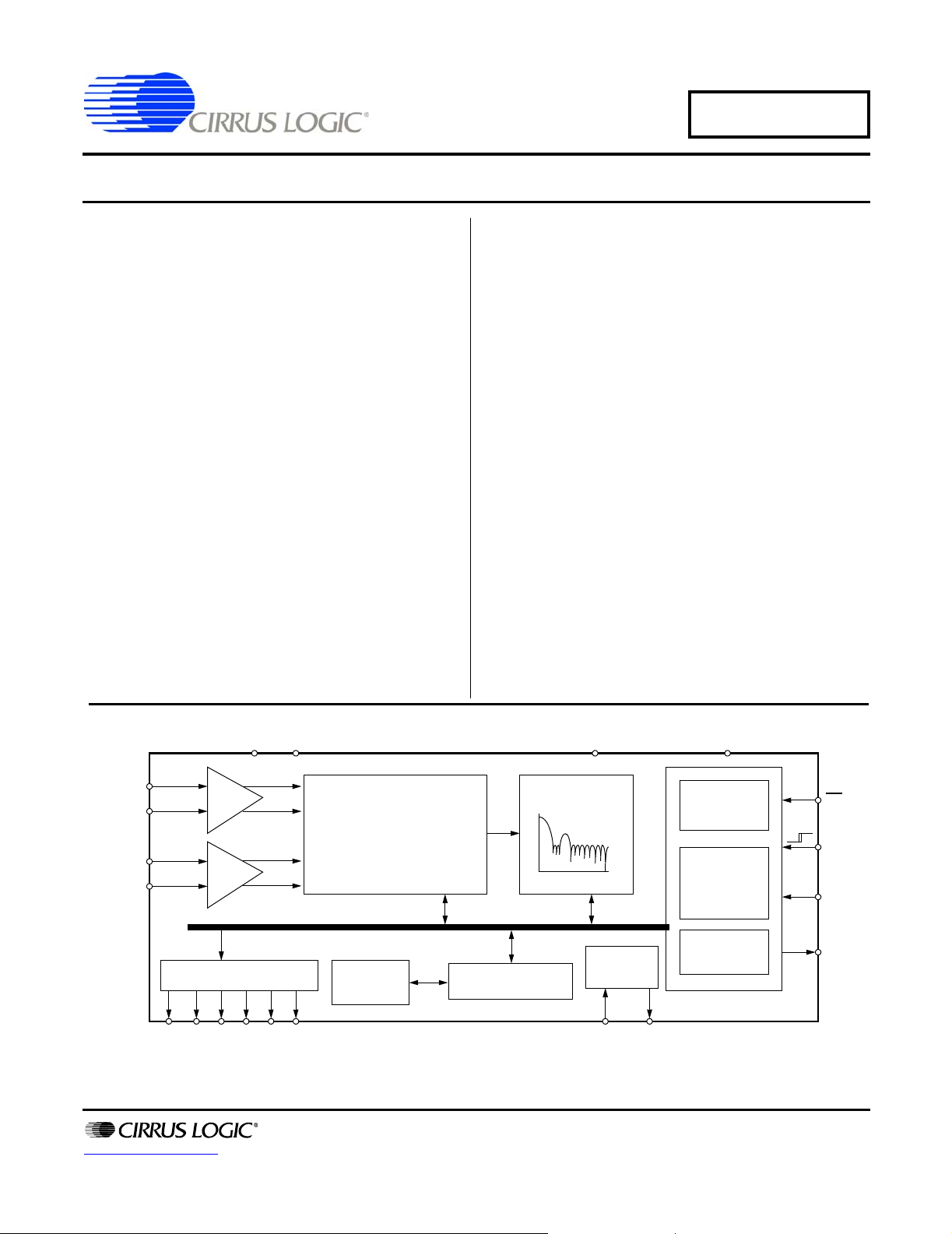
The 16-bit CS5529 is a low-power, programmable ∆Σ
ADC (Analog-to-Digital Converter), which includes
coarse/fine charge buffers, a fourth-order ∆Σ modulator,
a calibration microcontroller, a digital filter with programmable decimation rates, a 6-bit output latch, and a threewire serial interface. The ADC is designed to operate
from single or dual analog supplies and a single digital
supply.
The digital filter is programmable with output update
rates between 1.88 Hz to 101 Sps. These output rates
are specified for XIN = 32.768 kHz. Output word rates
can be increased by approximately 3X by using XIN =
100 kHz. The filter is designed to settle to full accuracy
for the selected output word rate in one conversion.
When operated at word rates of 15 Sps or less, the filter
rejects both 50 Hz and 60 Hz simultaneously.
Low power, single conversion settling time, programmable output rates, and the ability to handle negative input
signals make this single- or dual-supply product an ideal
solution for isolated and non-isolated applications.
ORDERING INFORMATION
See page 29.
AIN+
AIN-
VREF+
VREF-
A0 A1 D0 D1 D2 D3
http://www.cirrus.com
1X
1X
Latch
VA+
VA- DGND
Differential
4th Order
Delta-Sigma
Modulator
Calibration
Memory
Copyright © Cirrus Logic, Inc. 2005
(All Rights Reserved)
Calibration µC
Digital Filter
XIN XOUT
Clock
Gen.
VD+
Calibration
Register
Control
Register
Output
Register
CS
SCLK
SDI
SDO
AUG ‘05
DS246F5
1
Page 2

TABLE OF CONTENTS
CHARACTERISTICS & SPECIFICATIONS ........................................................4
ANALOG CHARACTERISTICS...................................................................4
ANALOG CHARACTERISTICS...................................................................5
5V DIGITAL CHARACTERISTICS .............................................................. 6
3 V DIGITAL CHARACTERISTICS ..................................... ... .... ... ... ... ........6
DYNAMIC CHARACTERISTICS ................................................................. 6
ABSOLUTE MAXIMUM RATINGS.............................................................. 7
SWITCHING CHARACTERISTICS .............................................................8
GENERAL DESCRIPTION .......................................................... ... ................... 10
Analog Input ............................. ... .... ... ... ... ....................................... ... .... .. 10
Analog Input Model ............... .... ...................................... .... ... ... ... .... .. 10
Voltage Reference Input Model .......................................................... 10
Serial Port .................................................................................................11
Command Register Descriptions ........................................................ 12
Serial Port Interface ...........................................................................13
Serial Port Initialization ....................................................................... 15
System Initialization ........................... .... ... ... ... .... ... ............................ 15
Configuration Register .............................................................................. 15
Latch Output Pins .................. ....................................... ... .... ... ... ... .... .. 15
Power Consumption ...........................................................................15
Output Word Rate ..............................................................................16
Digital Filter ........................................................................................16
Clock Generator .............................................. .... ............................... 16
Reset System ..................................................................................... 16
Port Flag ....................... ....................................... ... ... ... ... .... ... ............17
Calibration .......................................................................................... 17
Configuration Register Descriptions .................................................20
Performing Conversions ........................... .... ...................................... .... .. 21
Performing Conversions with PF bit = 0 ....... ... .... ... ... ... ... ....... ... ... .... .. 21
Performing Conversions with PF bit = 1 ....... ... .... ... ... ... ... ....... ... ... .... .. 21
Output Coding ....................................................................................22
............................................................................................................ 22
Power Supply Arrangements ....................................................................23
Getting Started ......................................................................................... 25
PCB Layout ........................... ... ... .... ... ... ... ....................................... ... .... .. 25
PIN DESCRIPTIONS ......................................................................................... 26
SPECIFICATION DEFINITIONS ........................................................................ 28
ORDERING INFORMATION ..............................................................................29
ENVIRONMENTAL, MANUFACTURING, & HANDLING INFORMATION ......29
PACKAGE DIMENSIONS .................................................................................30
CS5529
Calibration Registers ................................................................... 17
Offset Register ... ... ....................................... ... ... .... ... ... ... ......17
Gain Register ........................................................................ 18
Self Calibration ............................................................................ 18
System Calibration .............................. ....................................... .. 18
Limitations in Calibration Range .................................................. 19
Calibration Tips ............................................................................19
Single Conversion ........................................................................ 21
Continuous Conversions ........................ ...................................... 21
2 DS246F5
Page 3
LIST OF FIGURES
o
r
d
e
s
s
s
d
R
N
S
E
D
A
M
Y
o
Input models for AIN+ and AIN- pins......................................................... 11
Input model for VREF+ and VREF- pins. .................................................. 11
CS5529 Register Diagram. ....................................................................... 11
Command and Data Word Timing.............................. ...... ... ... .... ... ... ... .... .. 14
Filter Response (Normalized to Output Word Rate = 1)............................ 16
Self Calibration of Offset. .......................................................................... 18
Self Calibration of Gain. ............................................................................ 18
System Calibration of Offset...................................................................... 18
System Calibration of Gain........................................................................ 19
CS5529 Configured with a +5.0 V Analog Supply..................................... 23
CS5529 Configured with ±2.5 V Analog Supplies..................................... 23
CS5529 Configured with ±3.0 V Supplies. ................................................ 24
REVISION HISTORY
Revision Date Changes
CS5529
F4 Sep ‘04 Added lead-free device ordering information..
F5 Aug ‘05 Updated legal notice. Added MSL data.
Contacting Cirrus Logic Support
For all product questions and inquiries contact a Cirrus Logic Sales Representative.
To find the one nearest to you go to www.cirrus.com
IMPORTANT NOTICE
Cirrus Logic, Inc. and i ts subsidiaries (“Cirr us”) believe that the information contained in t his document is accurate and re liable. However, the information is subject t
change without notice and is provided “AS IS” without warranty of any kind (express or implied). Customers are advised to obtain the latest version of relevant info
mation to verify, before placing orders, that inform ation being relied on is current and complete. All prod ucts are sold subject to the term s and conditions of sale supp lie
at the time of order acknowl edgment, i ncludin g those per taining to warra nty, in demnifica tion, an d limitat ion of l iabili ty. No r esponsibility is assumed by Cirrus for th
use of this information, including use of this inform atio n as the basis for manufacture or sale of any items, or for infringement of patents or other rights of third partie
This document is the property of Cirrus and by furnishing this information, Cirrus grants no license, express or implied under any patents, mask work rights, copyright
trademarks, trade secrets or other intellectual property rights. Cirrus owns the copyrights associated with the information contained herein and gives consent for copie
to be made of the information on l y for use wi t h i n you r or g aniz a ti on wit h res p ect to Cirr u s integrated circuits or oth er pr od uct s of Cirr us . This con sen t do es no t exte n
to other copying such as copying for general distribution, advertising or promotional purposes, or for creating any work for resale.
CERTAIN APPLICATIONS USING SEMICONDUCTOR PRODUCTS MAY INVOLVE POTENTIAL RISKS OF DEATH, PERSONAL INJURY, OR SEVERE PROPE
TY OR ENVIRONMENTAL DAMAGE (“CRITICAL APPLICATIONS”). CIRRUS PRODUCTS ARE NOT DESIGNED, AUTHORIZED OR WARRANTED FOR USE I
AIRCRAFT SYSTEMS, MILITARY APPLICATIONS, PRODUCTS SURGICALLY IMPLANTED INTO THE BODY, AUTOMOTIVE SAFETY OR SECURITY DEVICE
LIFE SUPPORT PRODUCTS OR OTHER CRITICAL APPLICATIONS. INCLUSION OF CIRRUS PRODUCTS IN SUCH APPLICATIONS IS UNDERSTOOD TO B
FULLY AT THE CUSTOMER'S RISK AND CIRRUS DISCLAIMS AND MAKES NO WARRANTY, EXPRESS, STATUTORY OR IMPLIED, INCLUDING THE IMPLIE
WARRANTIES OF MERCHANTABILITY AND FITNESS FOR PARTICULAR PURPOSE, WITH REGARD TO ANY CIRRUS PRODUCT THAT IS USED IN SUCH
MANNER. IF THE CUSTOMER OR CUSTOMER'S CUSTOMER USES OR PERMITS THE USE OF CIRRUS PRODUCTS IN CRITICAL APPLICATIONS, CUSTO
ER AGREES, BY SUCH USE, TO FULLY INDEMNIFY CIRRUS, ITS OFFICERS, DIRECTORS, EMPLOYEES, DISTRIBUTORS AND OTHER AGENTS FROM AN
AND ALL LIABILITY, INCLUDING ATTORNEYS' FEES AND COSTS, THAT MAY RESULT FROM OR ARISE IN CONNECTION WITH THESE USES.
Cirrus Logic, Cirrus, and the Cirrus Logic logo designs are trademarks of Cirrus Logic, Inc. All other brand and product names in this docu ment may b e trademar ks
service marks of their respective owners.
DS246F5 3
Page 4
CHARACTERISTICS & SPECIFICATIONS
CS5529
ANALOG CHARACTERISTICS (T
VREF- = 0.0 V, F
(See Notes 1 and 2.)
Accuracy
Linearity Error - ±0.0015 ±0.003 %FS
No Missing Codes 16 - - Bits
Bipolar Offset (Note 3) - ±1 ±2 LSB
Unipolar Offset (Note 3) - ±2 ±4 LSB
Offset Drift (Notes 3 and 4) - 11 - nV/°C
Bipolar Gain Error - ±8 ±31 ppm
Unipolar Gain Error - ±16 ±63 ppm
Gain Drift (Note 4) - 1 - ppm/°C
Noise (Notes 5 and 6)
Output Word Rate (Hz) -3 dB Filter Frequency (Hz) Noise (µV)
= 32.768 kHz, OWR (Output Word Rate) = 15 Sps, Bipolar Mode, Input Range = ±2.5 V.)
CLK
Parameter Min Typ Max Unit
1.88 1.64 4.5
3.76 3.27 5.0
7.51 6.55 7.0
15.0 12.7 15
30.0 25.4 45
61.6 50.4 190
84.5 70.7 900
101.1 84.6 3000
= 25 °C; VA± = ±2.5 V ±5%, VD+ = 5 V ±5%, VREF+ = 2.5 V,
A
16
16
Notes: 1. Applies after system calibration at any temperature within -40 °C ~ +85 °C.
2. Specifications guaranteed by design, characterization, and/or test.
3. Specification applies to the device only and does not include any eff ec ts by external parasitic
thermocouples.
4. Drift over specified temperature range after calibration at power-up at 25 °C.
5. Wideband noise aliased into the baseband. Referred to the input. Typical values shown for 25 °C.
6. For peak-to-peak noise multiply by 6.6 for all ranges and output rates.
Specifications are subject to change without notice.
4 DS246F5
Page 5
CS5529
ANALOG CHARACTERISTICS (Continued)
Parameter Min Typ Max Unit
Analog Input
Common Mode + Signal on AIN+ or AIN- (Bipolar/Unipolar Mode)
Single Supply
Dual Supply
Common Mode Rejection dc
50, 60Hz
Input Capacitance - 10 - pF
CVF Current AIN+, AIN- (Note 7) - 16 - nA
System Calibration Specifications
Full Scale Calibration Range, with VREF = 2.5 V (Note 8) 1.0 - 3.5 V
Offset Calibration Range (Bipolar/Unipolar Mode) - - ±1.25 V
Voltage Reference Input
Range {(VREF+) - (VREF-)} (Note 9) 1.0 2.5 5 V
REF+ VA- - VA+ V
REF- VA- - VA+ V
Common Mode Rejection dc
50, 60 Hz
Input Capacitance - 16 - pF
CVF Current (Note 7) - 8 - nA
Power Supplies
DC Power Supply Currents (Normal Mode)
I
A+
I
D+
Power Consumption Normal Mode (Note 10)
Low Power Mode
Standby
Sleep
Power Supply Rejection dc Positive Supplies
dc Negative Supply
0.0
VA-
-
-
-
-
-
-
-
-
-
-
-
-
-
-
120
120
110
130
400
110
2.6
1.8
1
500
80
80
VA+
VA+
-
-
-
-
520
150
3.5
2.5
-
-
-
-
mW
mW
mW
µW
V
V
dB
dB
dB
dB
µA
µA
dB
dB
Notes: 7. See the section of the data sheet which discusses Analog Input Models.
8. The minimum Full Scale Calibration Range (FSCR) is limited by the maximum allowed gain register
value (with margin). The maximum FSCR is limited by the ∆Σ modulator’s 1’s density range. See
“Analog Input” section for details. Also see “Limitations in Calibration Range”.
9. VREF must be less than or equal to supply voltages.
10. All outputs unloaded. All inputs CMOS levels. Power consumption scales linearly with changes in
supply voltage.
DS246F5 5
Page 6
CS5529
5V DIGITAL CHARACTERISTICS (T
= 25 °C; VA± = ±2.5V ±5%, VD+ = 5V ± 5 % .)(See Notes 2 and
A
11.)
Parameter Symbol Min Typ Max Unit
High-level Input Voltage: All Pins Except XIN, SCLK
XIN
SCLK
Low-level Input Voltage: All Pins Except XIN, SCLK
XIN
SCLK
High-level Output Voltage: All Pins Except SDO (Note 12)
SDO, I
Low-level Output V oltage: All Pins Except SDO, I
SDO, I
= -5.0mA
out
= 1.6mA
out
= 5.0mA
out
Input Leakage Current I
3-state Leakage Current I
Digital Output Pin Capacitance C
Notes: 11. All measurements performed under static conditions.
12. I
= -100 µA unless stated otherwise. (VOH = 2.4 V @ I
out
out
V
IH
V
IH
IH
IL
IL
IL
OH
OH
OL
OL
in
OZ
out
(VD+)-0.45
V
V
V
V
V
V
V
V
= -40 µA).
0.6VD+
(VD+)-0.9
-
-
-
(VD+)-1.0
(VD+)-1.0--
-
-
-
-
-
-
-
-
-
-
-
-
-
0.8
2.0
0.6
-
-
0.4
0.4
-±1±10µA
--±10µA
-9-pF
V
V
V
V
V
V
V
V
V
V
3 V DIGITAL CHARACTERISTICS (T
= 25 °C; VA± = ±2.5 V ±5%, VD+ = 3.0 V ±5%.)
A
(See Notes 2 and 11.)
Parameter Symbol Min Typ Max Unit
High-level Input Voltage: All Pins Except XIN, SCLK
XIN
SCLK
Low-level Input Voltage: All Pins Except XIN, SCLK
XIN
SCLK
High-level Output Voltage: All Pins Except SDO, I
SDO, I
Low-level Output V oltage: All Pins Except SDO, I
SDO, I
= -400 µA
out
= -5.0 mA
out
= 400 µA
out
= 5.0 mA
out
Input Leakage Current I
3-state Leakage Current I
Digital Output Pin Capacitance C
DYNAMIC CHARACTERISTICS
Parameter Symbol Ratio Units
V
IH
V
IH
V
IH
V
IL
V
IL
V
IL
V
OH
V
OH
V
OL
V
OL
in
OZ
out
0.6VD+
(VD+)-0.9
(VD+)-0.45
-
-
-
(VD+)-0.3
(VD+)-1.0--
-
-
-±1±10µA
--±10µA
-9-pF
-
-
-
-
-
-
-
-
-
-
-
0.16 VD+
0.5
0.6
-
-
0.3
0.4
V
V
V
V
V
V
V
V
V
V
Modulator Sampling Frequency f
Filter Settling Time to 1/2 LSB (Full Scale Step) t
s
s
XIN/4 Hz
1/f
out
s
6 DS246F5
Page 7
CS5529
ABSOLUTE MAXIMUM RATINGS (DGND = 0 V) (See Note 13.)
Parameter Symbol Min Typ Max Unit
DC Power Supplies (Notes 14 and 15)
Positive Digital
Positive Analog
Negative Analog
Input Current, Any Pin Except Supplies (Notes 16 and 17) I
Output Current I
VD+
VA+
VA-
IN
OUT
-0.3
-0.3
-6.0
-
-
-
--±10mA
--±25mA
+6.0
+6.0
+0.3
Power Dissipation (Note 18) PDN - - 8 mW
Analog Input Voltage AIN and VREF pins V
Digital Input Voltage V
Ambient Operating Temperature T
Storage Temperature T
INA
IND
A
stg
(VA-) + (-0.3) - (VA+)+0.3 V
-0.3 - (VD+)+0.3 V
-40 - +85 °C
-65 - +150 °C
Notes: 13. All voltages with respect to ground.
14. VA+ and VA- must satisfy {(VA+) - (VA-)} ≤ +6.3 V; and |VA-| must be ≤ VA+.
15. VD+ and VA- must satisfy {(VD+) - (VA-)} ≤ +7.75 V.
16. Applies to all pins including continuous overvoltage conditions at the analog input (AIN) pins.
17. Transient current of up to 100mA will not cause SCR latch -up. Maximum input current for a power
supply pin is ±50 mA.
18. Total power dissipation, including all input currents and output currents.
V
V
V
WARNING: Operation at or beyond these limits may result in permanent damage to the device.
Normal operation is not guaranteed at these extremes.
DS246F5 7
Page 8
CS5529
SWITCHING CHARACTERISTICS (T
Input Levels: Logic 0 = 0 V, Logic 1 = VD+; C
= 50pF)
L
= 25 °C; VA ± = ±2.5 V ±5%, VD+ = 3 V ±5% or 5 V ±5%;
A
Parameter Symbol Min Typ Max Unit
Master Clock Frequency: External Clock or Internal Oscillator
XIN 30 32.768 100 kHz
(Note19)
Master Clock Duty Cycle 40 - 60 %
Rise Times (Note 20)
Any Digital Input Except SCLK
SCLK
Any Digital Output
Fall Times (Note 20)
Any Digital Input Except SCLK
SCLK
Any Digital Output
t
t
rise
rise
-
-
-
-
-
-
-
-
50
-
-
50
1.0
100
-
1.0
100
-
µs
µs
ns
µs
µs
ns
Start-up
Oscillator Start-up Time XTAL = 32.768 kHz (Note 21) t
Power-on Reset Period t
ost
por
-500-ms
- 1002 - XIN
cycles
Serial Port Timing
Serial Clock Frequency SCLK 0 - 2 MHz
Serial Clock Pulse Width High
Pulse Width Low
t
1
t
2
250
250
-
-
-
-
ns
ns
SDI Write Timing
CS
Enable to Valid Latch Clock t
Data Set-up Time prior to SCLK rising t
Data Hold Time After SCLK Rising t
SCLK Falling Prior to CS
Disable t
3
4
5
6
50 - - ns
50 - - ns
100 - - ns
100 - - ns
SDO Read Timing
to Data Valid t
CS
SCLK Falling to New Data Bit t
Rising to SDO Hi-Z t
CS
7
8
9
--150ns
--150ns
--150ns
Notes: 19. Device parameters are specified with 32.768 kHz clock, however, clocks up to 100 kHz can be used for
increased throughput.
20. Specified using 10% and 90% points on waveform of interest. Output loaded with 50 pF.
21. Oscillator start-up time varies with crystal parameters. This specification does not apply when using an
external clock source.
8 DS246F5
Page 9
CS
CS5529
SCLK
CS
SDI
SCLK
t3
MSB
t3
t1
t2
Continuous Running SCLK Timing (Not to Scale)
MSB-1
t2
t6
LSB
t6t4 t5 t1
SDI Write Timing (Not to Scale)
CS
SDO
t7
MSB MSB-1
t8
LSB
t2
t9
SCLK
t1
SDO Read Timing (Not to Scale)
DS246F5 9
Page 10

CS5529
GENERAL DESCRIPTION
The CS5529 is a 16-bit ∆Σ Analog-to-Digital Converter (ADC) which includes coarse/fine charge
buffers, a fourth order ∆Σ modulator, a calibration
microcontroller, eight digital filters which provide
selectable decimation rates, a 6-bit output latch,
and a three-wire serial interface. The ADC is optimized to digitize unipolar or bipolar signals in industrial applications.
The digital filters provide eight selectable output
word rates (OWRs) of 1.88 Sps, 3.76 Sps, 7.51 Sps,
15.0 Sps, 30.0 Sps, 61.6 Sps, 84.5 Sps, 101.1 Sps
when operated from a 32.768 kHz watch crystal or
equivalent clock (output word rates can be increased by approximately 3X by using 100 kHz
clock). The filters are designed to settle to full accuracy for the selected output word rate in one conversion. When operated at word rates of 15 Sps or
less (XIN = 32.768 kHz), the filter rejects both 50
Hz and 60 Hz line interference simultaneously.
Analog Input
The CS5529 provides a nominal 2.5 V input span
when the gain register is 1.0 decimal and the differential reference voltage between VREF+ and
VREF- is 2.5 V. The gain registers content is used
during calibration to set the gain slope of the
ADC’s transfer function. The differential reference
voltage magnitude and the gain register are two
factors that can be used to scale the nominal 2.5 V
input span. After reset, the gain register defaults to
1.0 decimal. In this case, the external voltage between the VREF+ pin and the VREF- pin sets the
ADC’s nominal full scale input span to 2.5 V. If a
user want to modify the input span, either the gain
register or the reference voltage’s magnitude needs
to be changed. For example, if a 1.25 V reference is
used in place of the nominal 2.5 V input, the fullscale span is cut in half. To achieve the same 1.25V
input span, the user could simply use a 2.5 V reference and modify the gain register to 2.0 decimal.
Note that to keep from saturating the analog front
end, the input span must stay at or below 1.5 times
the reference voltage. This corresponds to a gain
register of 0.666... when a 2.5 V reference voltage
is used.
Note: When a smaller reference voltage is used,
the resulting code widths are smaller. Since
the output codes exhibit more changing
codes for a fixed amount of noise, the
converter appears noisier.
Calibration can also affect the ADC’s full scale
span because system gain calibration can be used to
increase or decrease the full scale span of the
ADC’s transfer functions. At its limit, the input full
scale can be reduced to the point in which the gain
register reaches its upper limit of 3.999... (this will
occur when the ADC is gain calibrated with an input signal less than or equal to approximately 1/4 of
its nominal full scale, if the ADC does not have intrinsic gain error). Calibration and its effects on the
analog input span is detailed in a later section of the
data sheet.
Analog Input Model
Figure 1 illustrates the input models for the AIN
pins. The model includes a coarse/fine charge buffer which reduces the dynamic current demands
from the signal source. The buffer is designed to
accommodate rail to rail (common-mode plus signal) input voltages. Typical CVF (sampling) current is about 16nA (XIN = 32.768 kHz, see Figure
1). Application Note 30, “Switched-Capacitor A/D
Input Structures”, details various input architectures.
Voltage Reference Input Model
Figure 2 illustrates the input models for the VREF
pins. It includes a coarse/fine charge buffer which
reduces the dynamic current demand of the external reference. Typical CVF (sampling) current is
about 8nA (XIN = 32.768 kHz, see Figure 2).
The reference’s buffer is designed to accommodate
rail-to-rail (common-mode plus signal) input volt-
10 DS246F5
Page 11
AIN
Fine
φ
1
Coarse
φ
1
VREF
Fine
φ
1
Coarse
φ
2
CS5529
V ≤ 25m V
os
i = fV C
n
os
C = 20pF
f = 32.768 k H z
Figure 1. Input models for AIN+ and AIN- pins.
ages. The differential voltage between VREF+ and
VREF- sets the nominal full scale input span of the
converter. For a single-ended reference voltage,
such as the LT1019-2.5, the reference output is
connected to the VREF+ pin of the CS5529 and the
ground reference for the LT1019-2.5 is connected
to the VREF- pin.
Serial Port
The CS5529 includes a microcontroller with a
command register, a configuration register, a conversion data register (read only), and a gain and offset register for calibration. All registers, except the
8-bit command register, are 24-bits in length. Fig-
V ≤ 25m V
os
i = fV C
n
os
C = 10pF
f = 32.768 kHz
Figure 2. Input model for VREF+ and VREF- pins.
ure 3 illustrates a block diagram of all the internal
register.
After a system initialization or reset, the serial port
is set to the command mode. The converter stays in
this mode until a valid 8-bit command is received
(the first 8-bits into the serial port). Once a valid 8bit command is received and interpreted by the
ADC’s command register, the serial port enters the
data mode. In data mode the next 24 serial clock
pulses shift data either into or out of the serial port
(72 serial clock pulses are needed if the setup register command is issued). The Command Register
Descriptions section illustrates all valid commands.
Conversion Data Register (1x24)
Gain Register ( 1 × 24)Offset Register (1 × 24)
Read Only
Serial
Interface
Configuration Register (1 × 24)
Latch Outputs
Low Power Mode
Output Word Rate s
Unipolar/Bipolar
Reset System
etc.
Figure 3. CS5529 Register Diagram.
DS246F5 11
Write Only
Command Register (1 × 8)
CS
SDI
SDO
SCLK
Page 12

Command Register Descriptions
D7(MSB)D6D5D4D3D2D1D0
CS5529
CB SC CC R/W
RSB2 RSB1 RSB0 PS/R
BIT NAME VALUE FUNCTION
D7 Command Bit, CB 0
Null command (no operation). All command bits,
including CB must be 0.
Logic 1 for executable commands.
Single Conversion not active.
Perform a conversion.
Continuous Conversions not active.
Perform conversions continuously.
Write to selected register.
Read from selected register.
Offset Register
Gain Register
Configuration Register
Conversion Data Register (read only)
Set-up Registers (Offset, Gain, Configuration)
Reserved
Reserved
Reserved
Run
Power Save
D6 Single Conversion, SC 0
D5 Continuous Conversions,
CC
D4 Read/Write
D3-D1 Register Select Bit, RSB2-
RSB0
, R/W 0
000
001
010
011
100
101
110
111
D0 Power Save/Run
, PS/R 0
1
1
0
1
1
1
Table 1. Command Set
Perform Single Conversion
76543210
11000000
This command instructs the ADC to perform a single conversion.
Perform Continuous Conversions
76543210
10100000
This command instructs the ADC to perform continuous conversions.
Power Save/Run
76543210
1000000PS/R
If PS/R = 0, normal run mode is entered. If PS/R = 1, power save mode is entered.
Null
76543210
00000000
This command is used to clear the port flag in the continuous conversion mode when the port flag bit in the configuration register
is set to logic 1.
12 DS246F5
Page 13
CS5529
SYNC1
76543210
11111111
Part of the serial port re-initialization sequence (see text for use of command).
SYNC0
76543210
11111110
End of the serial port re-initialization sequence.
Read/Write
76543210
100R/W
These commands are used to perform a write to or a read from a specific register . The register to be accessed is
selected with the RSB2-RSB0 bits of the command word.
R/W
RSB[4:0] Register address binary encoded 0 to 31 as follows. All registers are 24 bits long.
Serial Port Interface
The CS5529’s serial interface consists of four control lines: CS
Registers
RSB2 RSB1 RSB0 0
0 Write Register
1 Read Register
Address
000 Read or Write Offset Register
001 Read or Write Gain Register
010 Read or Write Configuration Register
011 Read Conversion Data Register
100 Read or Write Offset Gain and Configura tion Re gisters in
Description
this sequence (i.e. one 8-bit command is followed by 72-bits of
data to access the Offset, then the Gain, and then the
Configuration register)
port logic. To accommodate opto-isolators SCLK
is designed with a Schmitt-trigger input to allow an
, SDI, SDO, and SCLK.
opto-isolator with slower rise and fall times to directly drive the pin. Additionally, SDO is capable
CS
, Chip Select, is the control line which enables
access to the serial port. If the CS pin is tied to logic
0, the port can function as a three wire interface.
SDI, Serial Data In, is the data signal used to transfer data to the converters.
SDO, Serial Data Out, is the data signal used to
transfer output data from the converters. The SDO
output will be held at high impedance any time CS
is at logic 1.
SCLK, Serial Clock, is the serial bit-clock which
controls the shifting of data to or from the ADC’s
serial port. The CS
pin must be held at logic 0 be-
fore SCLK transitions can be recognized by the
of sinking or sourcing up to 5 mA to directly drive
an opto-isolator LED. SDO will have less than a
400 mV loss in the drive voltage when sinking or
sourcing 5 mA.
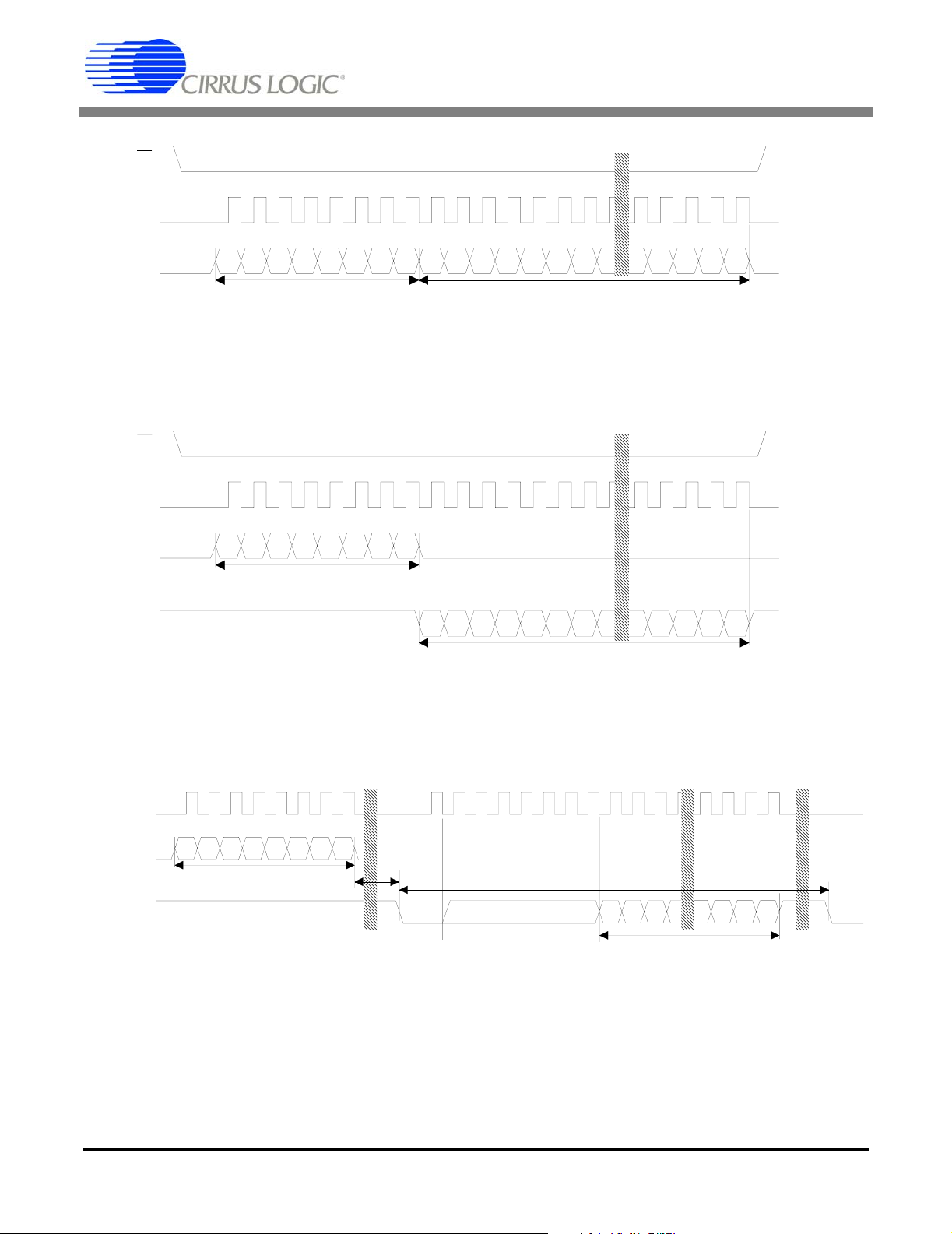
Figure 4 illustrates the serial sequence necessary to
write to, or read from the serial port’s registers. A
transfer of data is always initiated by sending the
appropriate 8-bit command (MSB first) to the serial
port (SDI pin). It is important to note that some
commands use information from the configuration
registers to perform the function. For those commands it is important that the correct information is
written to the configuration register first.
DS246F5 13
Page 14
CS
SCLK
CS5529
SDI
CS
SCLK
SDI
SDO
Command Time
8 SCLKs
Command Time
8 SCLKs
MSB
Write Cycle
MSB
Read Cycle
LSB
Data Time 24 SCLKs
(or 72 SCLKs for Set-up Registers)
LSB
Data T im e 2 4 SC LKs
(or 72 S C LKs for S et-up R egisters)
SCLK
SDI
t *
Command Time
8 SCLKs
SDO
* td = XIN/OWR clock cycles for each conversion except the
first conversion which will take XIN/OWR + 7 clock cycles
d
SDO Continuous Conversion Read (PF bit = 1)
8 SCLKs Clear SDO Flag
MSB
Data Time
24 SCLKs
XIN/OWR
Clock Cycles
LSB
Figure 4. Command and Data Word Timing.
14 DS246F5
Page 15

CS5529
Serial Port Initialization
The serial port is initialized to the command mode
whenever a power-on reset is performed or when
the port initialization sequence is completed. The
port initialization sequence involves clocking fifteen (or more) SYNC1 command bytes (0xFF) followed by one SYNC0 command byte (0xFE). This
sequence places the chip in the command mode
where it waits until a valid command is received.
This function does not reset the internal registers to
their default settings. It only resets the serial port to
the command mode.
System Initialization
When power to the CS5529 is applied, the chip is
held in a reset condition until the 32.768 kHz oscillator has started and a counter-timer elapses. Due to
the high Q of the 32.768 kHz crystal, the oscillator
takes 400-600 ms to start. The counter-timer counts
1002 oscillator clock cycles to make sure the oscillator is fully stable. During this time-out period the
serial port logic is reset and the RV (Reset Valid)
bit in the configuration register is set to indicate
that a valid reset occurred. After a reset, the on-chip
registers are initialized to the following states and
the converter is placed in the command mode
where it waits for a valid command.
Configuration Register: 000040(H)
Offset Register: 000000(H)
Gain Register: 400000(H)
Latch Output Pins
The D3-D0 pins of the converter mimic the D21D18 bits of the configuration register. D3-D0 can
be used to control multiplexers and other digital
logic functions outside the converter. The D0-D3
outputs are powered from VD+ and DGND. Their
output voltage will be VD+ for a logic 1 and
DGND for a logic 0. The A1-A0 pins of the converter mimic the D23-D22 bits of the configuration
register and can be used to control analog switches.
These outputs are powered from VA+ and VA-,
hence, their output voltage will be either VA+ for a
logic 1 or VA- for a logic 0.
All outputs can sink or source at least 1 mA, but it
is recommended to limit drive currents to less than
20 µA to reduce self-heating of the chip.
Power Consumption
The CS5529 accommodates four power consumption modes: normal, low power, standby, and sleep.
The normal mode, the default mode, is entered after
a power-on-reset and typically consumes 2.5 mW.
The low power mode is an alternate mode that reduces the consumed power to 1.4 mW. It is entered
by setting bit D16 (the low power mode bit) in the
configuration register to logic 1. Since the converter’s noise and linearity performance improves with
increased power consumption, slightly degraded
noise or linearity performance should be expected
in the low power mode.
Note: A system reset can be initiated at any time by
writing a logic 1 to the RS (Reset System) bit
in the configuration register. After a reset, the
RV (Reset Valid) bit is set until the
configuration register is read. The user must
then write a logic 0 to the RS bit to take the
part out of the reset mode.
Configuration Register
The configuration register is a 24 bit register used
to modify the functions of the ADC. The following
sections detail the functions of the bits in the configuration register.
DS246F5 15
The final two modes are the power save modes.
These modes power down most of the analog portion of the chip and stop filter convolutions. The
power save modes are entered whenever the Power
Save (0x81 hexadecimal) command is issued to the
serial port. The particular power save mode entered
depends on state of bit D4 (the power save select
bit) in the configuration register. If D4 is logic 0,
the converter enters the standby mode reducing the
power consumption to 1 mW. The standby mode
leaves the oscillator and the on-chip bias generator
Page 16

CS5529
running. This allows the converter to quickly return
to the normal or low power mode once the PS/R bit
is set back to a logic 0. If D4 in the configuration
register is logic 1 and Power Save command is issued, the sleep mode is entered reducing the consumed power to less than 10 µW. Since the sleep
mode disables the oscillator, approximately a 500
ms crystal oscillator start-up delay period is required before returning to the normal or low power
mode. If an external clock is used, the chip should
start within a few microseconds.
Output Word Rate
The WR2-WR0 bits of the configuration register
set the output conversion word rate of the converter
as shown in the Configuration Register Descriptions table. The word rates indicated in the table assume a master clock of 32.768 kHz. Upon reset the
converter is set to operate with an output word rate
of 15.0 Sps.
better than 80 dB rejection for both 50 Hz and
60 Hz with output word rates at or below 15.0 Sps
(XIN = 32.768 kHz).
The converter’s digital filters scale with XIN. For
example with an output word rate of 15 Sps, the filter’s corner frequency is typically 12.7 Hz. If XIN
is increased to 64.536 kHz the OWR doubles and
the filter’s corner frequency moves to 25.4 Hz.
Clock Generator
The CS5529 includes a gate which can be connected with an external crystal to provide the master
clock for the chip. The chip is designed to operate
using a low-cost 32.768 kHz “tuning fork” type
crystal. One lead of the crystal should be connected
to XIN and the other to XOUT. Lead lengths
should be minimized to reduce stray capacitance.
Note that the converter will operate with an external (CMOS compatible) clock with frequencies up
to 100 kHz.
Digital Filter
The CS5529 has eight different linear phase digital
filters which set the output word rates (OWRs) as
stated in Configuration Register Descriptions.
These rates assume that XIN is 32.768 kHz. Each
of the filters has a magnitude response similar to
that shown in Figure 5. The filters are optimized to
settle to full accuracy every conversion and yield
Figure 5. Filter Response
(Normalized to Output Word Rate = 1).
Reset System
The reset system bit permits the user to perform a
hardware reset. A hardware reset can be initiated at
any time by writing a logic 1 to the RS (Reset System) bit in the configuration register. After a hardware reset cycle is complete, the serial port logic is
reset and the RV (Reset Valid) bit in the configuration register is set to indicate that a valid reset occurred. After a reset, the on-chip registers are
initialized to the following states and the converter
is placed in the command mode where it waits for
a valid command.
Configuration Register: 000040(H)
Offset Register: 000000(H)
Gain Register: 400000(H)
Note: A system reset can be initiated at any time by
writing a logic 1 to the RS (Reset System) bit
in the configuration register. After a reset, the
RV (Reset Valid) bit is set until the
configuration register is read. The user must
then write a logic 0 to the RS bit to take the
part out of the reset mode.
16 DS246F5
Page 17
CS5529
Port Flag
The port flag bit in the configuration register allows
the user to select the mode in which conversions
will be presented to the serial port. With the port
flag bit cleared, the user must read the conversion
data register. With the port flag bit set to logic 1, the
user can read the conversion data from the serial
port by first issuing the NULL command to clear
the SDO flag and then issuing 24 SCLKs to read
the conversion word.
Calibration
Calibration is used to set the zero and gain slope of
the ADC’s transfer function. The calibration control bits in the configuration register allow the user
to perform either self calibration or system calibration.
The offset and gain calibration steps each take one
conversion cycle to complete. At the end of the calibration step, the calibration control bits will be set
back to logic 0, and the DF (Done Flag) bit will be
set to a logic 1. For the combination self-calibration
(CC2-CC0= 011; offset calibration followed by
gain calibration), the calibration will take two con-
version cycles to complete and will set the DF bit
after the gain calibration is completed.
Note: 1) The DF bit will be cleared any time the data
register, the offset register, the gain register,
or the setup register is read. Reading the
configuration register alone will not clear the
DF bit.
2) After the CS5529 is reset, the converter is
functional and can perform measurements
without being calibrated. In this case, the
converter will utilize the initialized values of
the on-chip registers (Gain = 1.0, Offset = 0.0)
to calculate output words. Any initial offset
and gain errors in the internal circuitry of the
chip will remain.
Calibration Registers
The offset calibration result is stored in the offset
register. The result is used during the conversion
process to nullify offset errors. One LSB in the offset register is 2
polar span is 2 times the unipolar span). The MSB
in the offset register determines if the offset to be
trimmed is positive or negative (0 positive, 1 negative). The converter can typically trim ±50 percent
of the input span. Refer to the following Offset
Register and Gain Register descriptions for details.
-24
proportion of the input span (bi-
Offset Register
23(MSB) 22 21 20 19 18 17 16 15 14 13 12
Sign
0 00000 0 0 0 0 0 0
11 109876 5 4 3 2 1 0
-13
2
0 00000 0 0 0 0 0 0
-2
2
-14
2
One LSB represents 2
Offset and data word bits align by MSB (bit MSB-4 of offset register changes b it MSB-4 of data ). After rese t, all bits
are ‘0’.
DS246F5 17
-3
2
-15
2
-24
proportion of the input span (bipolar span is 2 times unipolar span).
-4
2
-16
2
-5
2
-17
2
-6
2
-18
2
-7
2
-19
2
-8
2
-20
2
-9
2
-21
2
-10
2
-22
2
-11
2
-23
2
-12
2
-24
2
Page 18
CS5529
Gain Register
23(MSB) 22 21 20 19 18 17 16 15 14 13 12
1
2
0 00000 0 0 0 0 0 0
11 109876 5 4 3 2 1 0
-11
2
0 00000 0 0 0 0 0 0
0
2
-12
2
-1
2
-13
2
-2
2
-14
2
-3
2
-15
2
-4
2
-16
2
-5
2
-17
2
-6
2
-18
2
-7
2
-19
2
-8
2
-20
2
-9
2
-21
2
-10
2
-22
2
The gain register span is from 0 to (4-2
-22
). After Reset the (MSB-1) bit is ‘1’, all other bits are ‘0’.
The gain calibration results is stored in the gain
register. The result sets the slope of the ADC’s
transfer function. The gain register spans from 0 to
-22
(4 - 2
). The decimal equivalent meaning of the
gain register is
N
Db
MSB
21b(020b121–… bN2N–)++++ b
1
2
+==
MSB
i 0=
∑
bi2
i–
where the binary numbers have a value of either
zero or one (b
corresponds to bit MSB-1, N = 22).
0
Self Calibration
The CS5529 offers both self offset and self gain
calibrations. For the self-calibration of offset, the
converter internally ties the inputs of the modulator
together and routes them to the VREF- pin as
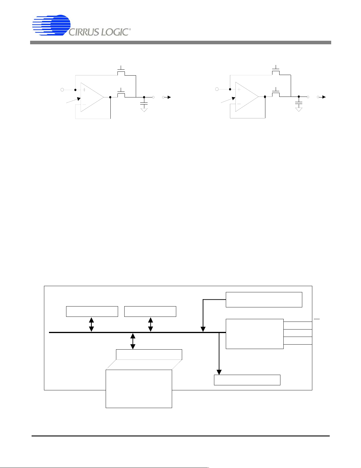
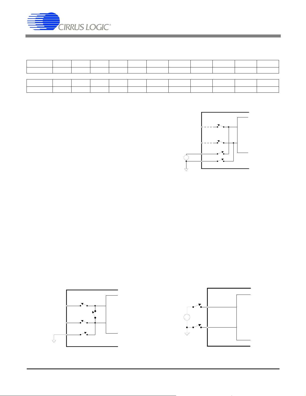
shown in Figure 6. Also self offset calibration requires that VREF- be tied to a fixed voltage between VA+ and VA-. For self-calibration of gain,
the differential inputs of the modulator are connected to VREF+ and VREF- as shown in Figure7.
OPEN
Reference
+
-
AIN+
AIN-
VREF+
VREF-
OPEN
CLOSED
CLOSED
+
-
Figure 7. Self Calibration of Gain.
System Calibration
For the system calibration functions, the user must
input signals which represent system ground and
system full scale to the converter. When a system
offset calibration is performed a ground reference
signal must be applied to the converter (see Figure
8). When a system gain calibration is performed,
the user must input a signal representing the positive full scale point as shown in Figure 9. In either
case, calibration signals must be within the specified calibration limits for each specific calibration
step (refer to the System Calibration Specifica-
S1
AIN+
AIN-
VREF-
OPEN
S2
OPEN
S4
CLOSED
S3
CLOSED
+
-
Figure 6. Self Calibration of Offset.
External
Connections
+
-
0V
AIN+
+
-
AIN-
Figure 8. System Calibration of Offset.
18 DS246F5
Page 19

Calibration Tips
CS5529
External
Connections
AIN+
Full Scale
Figure 9. System Calibration of Gain.
+
-
AIN-
+
-
tions). If a system gain calibration is performed, the
calibrated input must not cause the resulting gain
register’s content, decoded in decimal, to exceed
3.9999998. The above condition requires that the
full scale input voltage to be greater than 25 percent
of the differential reference voltage (i.e. a 625mV
input signal must be applied if the differential reference voltage is 2.5V).
Limitations in Calibration Range
System calibration can be limited by signal headroom in the analog signal path inside the chip as
discussed under the Analog Input section of this
data sheet. For gain calibration the full scale input
signal can be reduced to the point in which the gain
register reaches its upper limit of (4-2
or FFFFFF (hexadecimal). Under nominal conditions, this occurs with a full scale input signal equal
to about 1/4 the reference voltage. With the converter’s intrinsic gain error, this full scale input signal may be higher or lower. In defining the
minimum Full Scale Calibration Range (FSCR)
under “Analog Characteristics”, margin is retained
to accommodate the intrinsic gain error. Alternatively the input full scale signal can be increased to
a point which exceeds the operating range of the
analog circuitry. This occurs when the input voltage is approximately 1.5X the differential reference voltage (Gain Register = 1.0).
-22
decimal)
Calibration steps are performed at the output word
rate selected by the WR2-WR0 bits of the configuration register. Since higher word rates result in
conversion words with more peak-to-peak noise,
calibration should be performed at lower output
word rates. Also, to minimize digital noise near the
device, the user should wait for each calibration
step to be completed before reading or writing to
the serial port.
Factory calibration can be performed in a user’s
system by using the system calibration capabilities
of the CS5529. After the ADC is calibrated in the
user’s system, the offset and gain register contents
can be read by the system microcontroller and recorded in EEPROM. These same calibration words
can then be uploaded into the offset and gain registers of the converter when power is first applied to
the system.
A user can scale the input range by modifying the
gain register. For example, if a self or system calibration is performed with a full scale of 2.5 V and
a full scale of 1.25 V is desired, the user can modify
the gain register to double its slope. This can be
done by reading the gain register, shifting the binary word one position to the left (this multiplies the
gain word by 2), and writing this word back into the
gain register. The gain register can be scaled by any
amount as long as it does not exceed a decimal
range of 0.25 to 4.0.
One of two methods can be used to determine when
a calibration is complete: 1) if the PF (Port Flag) bit
of the configuration register is set to logic 1, SDO
falls to logic 0 at the completion of a calibration; or
2) regardless of the PF bit, the DF (Done Flag) bit
in the configuration register is set at completion of
calibration. The user can either monitor the DF bit
or SDO to determine when a calibration is complete. Whichever method is used, the calibration
control bits (CC2-CC0) automatically return to logic 0 upon completion of any calibration.
DS246F5 19
Page 20

CS5529
Configuration Register Descriptions
D23(MSB) D22 D21 D20 D19 D18 D17 D16 D15 D14 D13 D12
A1 A0 D3 D2 D1 D0 NU LPM WR2 WR1 WR0 U/B
D11 D10 D9 D8 D7 D6 D5 D4 D3 D2 D1 D0
NU NU NU NU RS RV PF PSS DF CC2 CC1 CC0
BIT NAME VALUE FUNCTION
D23-D22 Latch Outputs, A1-A0 00 R* Latch Output Pins A1-A0 mimic the D23-D22 Register bits.
D21-D18 Latch Outputs, D3-D0 0000 R* Latch Output Pins D3-D0 mimic the D21-D18 Register bits.
D17 Not Used, NU 0 R Must always be logic zero.
D16 Low Power Mode,
LPM
D15-D13 Word Rate, WR2-0
(Note: Rates valid for
XIN = 32.768 kHz)
D12 Unipolar/Bipolar
D11-D8 Not Used, NU 0 R Must always be logic 0.
D7 Reset System, RS 0
D6 Reset Valid , RV 0
D5 Port Flag, PF 0
D4 Power Save Select,
PSS
D3 Done Flag, DF 0
D2-D0 Calibration Control
Bits, CC2-CC0
* R indicates the bit value after the part is reset
, U/B 0
0
R Normal Mode (≅ 2.5 mW)
1
000
001
010
011
100
101
110
111
000
001
010
011
100
101
110
111
R 15.0 Sps (2180 XIN cycles)
R Bipolar Measurement mode
1
R Normal Operation
1
1R
R Port Flag mode inactive
1
0
R Standby Mode (Oscillator active, allows quick power-up)
1
R Done Flag bit is cleared (read only).
1
R Normal operation (no calibration)
Reduced Power Mode (≅ 1 mW)
30.0 Sps (1092 XIN cycles)
61.6 Sps (532 XIN cycles)
84.5 Sps (388 XIN cycles)
101.1 Sps (324 XIN cycles)
1.88 Sps (17444 XIN cycles)
3.76 Sps (8724 XIN cycles)
7.51 Sps (4364 XIN cycles)
Unipolar Measurement mode
Activate a Reset cycle. To return to normal operation this bit must
be written back to logic zero.
No reset has occurred or bit has been cleared (read only) .
Valid Reset has occurred. (Cleared when read.)
Port Flag mode active
Sleep Mode (Oscillator inactive)
Calibration or Conversion cycle completed (read only).
Offset -- Self-Calibration
Gain -- Self-Calibration
Offset self-cal followed by Gain self-calibration
Not Used.
Offset -- System Calibration
Gain -- System Calibration
Not Used.
20 DS246F5
Page 21

CS5529
Performing Conversions
The CS5529 offers two modes of performing conversions: single conversion and continuous conversions. The sections that follow detail the
differences and provides examples illustrating how
to use the modes. Note that it is assumed that the
configuration register has been initialized before
conversions are performed.
Performing Conversions with PF bit = 0
A single conversion is performed after the user
transmits the single conversion command (0xC0
Hexadecimal). At the completion of the conversion, the DF (Done Flag) bit of the configuration
register will be set to a logic 1. While the conversion is being performed, the user can read the configuration register to determine if the DF bit is set.
Once DF has been set, the read conversion data register command (0x96 Hexadecimal) can be issued
to read the conversion data register to obtain the
conversion data word.
Note: 1)The DF bit of the configuration register will
be cleared to logic 0 when the conversion
data register, the gain register, or the offset
register is read. Reading only the
configuration register will not clear the DF flag
bit.
2) If another single conversion command is
issued to the converter while it is performing
a conversion, the filter will abandon the
current conversion and restart a new
convolution cycle.
Performing Conversions with PF bit = 1
The PF (Port Flag) bit in the configuration register
eliminates the need for the user to monitor the DF
(Done Flag) in the configuration register to determine if the conversion is available. When PF is set
to a logic 1, SDO’s output pin behaves as a flag signal indicating when conversions are completed.
SDO will fall to logic 0 once a new conversion is
complete.
Single Conversion
A single conversion is performed after the user
transmits the single conversion command (0xC0
Hexadecimal). At the completion of the conversion, SDO will fall to logic 0 to indicate that the
conversion is complete. To acquire the conversion,
the user must issue 8 SCLKs with SDI = logic 0
(i.e. the NULL command) to clear the SDO flag.
Upon the falling edge of the 8th SCLK, the SDO
pin will present the first bit (MSB) of the conversion word. 24 SCLKs (high, then low) are then required to read the conversion word from the port.
Note: 1) The user must not give an explicit
command (other than the NULL command) to
read the conversion data register when the
PF bit is set to logic 1.
2) The data conversion word must be read
before a new command can be entered a s the
converter will remain in the data mode until
the conversion word is read.
3) Once the conversion is read the converter
returns to the command mode.
Continuous Conversions
Continuous conversions are performed after the
user transmits the continuous conversions command (0xA0 Hexadecimal). At the completion of a
conversion, SDO will fall to logic 0 to indicate that
the conversion is complete. To read the conversion
word, the user must issue 8 SCLKs with SDI = logic 0 (i.e. the NULL command) to clear the SDO
flag. Upon the falling edge of the 8th SCLK, the
SDO pin will present the first bit (MSB) of the conversion word. 24 SCLKs (high, then low) are then
required to read the conversion word from the port.
When operating in the continuous conversion
mode, the user need not read every conversion. If
the user chooses not to read a conversion after SDO
falls, SDO will rise one XIN clock cycle before the
next conversion word is available and then fall
again to signal that another conversion word is
available. To exit the continuous conversion mode,
the user must issue any valid command, other than
the NULL command, to the SDI input when the
DS246F5 21
Page 22

CS5529
SDO flag falls. For instance, the user can just read
the conversion data register again to exit the continuous conversion mode.
Note: 1) If the user begins to clear the SDO flag and
read the conversion data, this action must be
finished before the conversion cycle which is
occurring in the background is complete if the
user wants to be able to read the new
conversion data.
2) If a CC command is issued to the converter
while it is performing a conversion, the filter
will stop the current conversion and start a
new convolution cycle to perform a new
conversion.
3) Continuous conversions aren’t allowed
unless the port flag bit is set in the
configuration register.
4) The converter will remain in data mode and
continually perform conversions until the exit
command is issued (i.e. to exit the user must
read a register).
Output Coding
As shown in the Output Conversion Data Register
Descriptions, the CS5529 presents output conversions as a 24-bit conversion word. The first 16 bits
of the conversion word represent conversion data.
The third byte contains two error flag bits.
In the third byte, D7-D4 are always logic 1; D3-D2
are always logic 0; and bits D1-D0 are the two flag
bits. The OF (Overrange Flag) bit is set to a logic 1
any time the input signal is: 1) more positive than
positive full scale, 2) more negative than zero (unipolar mode), 3) more negative than negative full
scale (bipolar mode). It is cleared back to logic 0
whenever a conversion word occurs which is not
overranged.The OD ( Os ci ll at io n D et ec t) bit is s et t o
a logic 1 any time that an oscillatory condition is detected in the modulator. This does not occur under
normal operating conditions, but may occur whenever the input to the converter is extremely overranged. If the OD bit is set, the conversion data bits
can be completely erroneous. The OD flag bit will be
cleared to logic 0 when the modulator becomes stable.
Table 2 and Table 3 illustrate the output coding for
the CS5529. Unipolar conversions are output in binary format and bipolar conversions are output
two's complement.
D23 D22 D21 D20 D19 D18 D17 D16 D15 D14 D13 D12
MSB 1413121110 9 8 7 6 5 4
D11 D10 D9 D8 D7 D6 D5 D4 D3 D2 D1 D0
3 2 1 LSB 1 1 1 1 0 0 OD OF
Table 2. Output Conversion Data Register Description (16 bits + flags).
Unipolar Input Voltage Offset Binary Bipolar Input Voltage
>(VFS-1.5 LSB) FFFF >(VFS-1.5 LSB) 7FFF
FFFF
VFS-1.5 LSB
VFS/2-0.5 LSB
+0.5 LSB
<(+0.5 LSB) 0000 <(-VFS+0.5 LSB) 8000
Note: VFS in the table equals the voltage between ground and full scale for any of the unipolar gain ranges,
or the voltage between ± full scale for any of the bipolar gain ranges. See text about error flags under
overrange conditions.
Table 3. CS5529 16-bit Output Coding.
-----
FFFE
8000
-----
7FFF
0001
-----
0000
VFS-1.5 LSB
-0.5 LSB
-VFS+0.5 LSB
Two's
Complement
7FFF
-----
7FFE
0000
-----
FFFF
8001
-----
8000
22 DS246F5
Page 23

CS5529
Power Supply Arrangements
The CS5529 is designed to operate from single or
dual analog supplies and a single digital supply.
The following power supply connections are possible:
VA+ = +5 V; VA- = 0 V; VD+ = +3 V to +5 V
+5.0 V
Analog
Supply
±5 V Differential Inputs (Gain Register = 1.0)
±2.5 V Differential Inputs (Gain Register = 2.0)
±1.25 V Differenti al Inputs (Gain Regist er = 4.0)
Common Mode = 0 to VA+
0.1 µF
+
-
VA+ = +2.5 V; VA- = -2.5 V; VD+ = +3 V to +5 V
VA+ = +3.0 V; VA- = -3.0 V; VD+ = +3 V
Figure 10 illustrates the CS5529 connected with a
single +5 V supply to measure differential inputs
relative to a common mode of 2.5 V. Figure 11 illustrates the CS5529 connected with ±2.5 V bipolar
Ω
10
µ
0.1
213
CS5529
1
VD+
XOUT
XIN
SCLK
SDI
SDO
DGND
12
CS
10
11
8
9
15
14
VA+
20
VREF+
19
VREF-
3
AIN+
4
AIN-
18
D3
17
D2
16
D1
7
D0
6
A1
5
A0
VA-
F
32.768 kHz ~ 100 kHz
Optional Clock
Source
Serial
Data
Interface
Logic Outputs:
A0, A1 Switch from VA+ to VAD0-D3 Switch from VD+ to DGND
Figure 10. CS5529 Configured with a +5.0 V Analog Supply.
+2.5 V
Analog
Supply
±2.5 V Differential Inputs (Gain Register = 1.0)
±1.25 V Differential Inputs (Gain Register = 2.0)
±625 mV Diffe rential Inputs (Gain Re gister = 4.0)
-2.5 V
Analog
Supply
Logic Outputs:
A0, A1 Switch from VA+ to VAD0-D3 Switch from VD+ to DGND
0.1 µF
20
19
213
VA+
VREF+
VREF-
7
6
5
0.1 µF
AIN+
AIN-
D3
D2
D1
D0
A1
A0
CS5529
VA-
1
3
4
18
17
16
VD+
XOUT
XIN
SCLK
SDI
SDO
DGND
12
CS
10
32.768 kHz ~ 100 kHz
11
8
9
15
14
Figure 11. CS5529 Configured with ±2.5 V Analog Supplies.
+3 V ~ +5 V
µ
F
0.1
Optional Clock
Source
Serial
Data
Interface
Digital
Supply
DS246F5 23
Page 24

CS5529
analog supplies and a +3 V to +5 V digital supply
to measure ground referenced bipolar signals. Figure 12 illustrates the CS5529 connected with ±3.0
+3.0 V
Analog
Supply
±3.0 V Differential Inputs (Gain Register = 1.0)
±1.50 V Differential Inputs (Gain Register = 2.0)
±750 mV Differential Inputs (Gain Register = 4.0)
-3.0 V
Analog
Supply
Logic Outputs:
A0, A1 Switch from VA+ to VAD0-D3 Switch from VD+ to DGND
Figure 12. CS5529 Configured with ±3.0 V Supplies.
0.1µF
V bipolar analog supplies and a +3 V digital supply
to measure ground referenced bipolar signals.
+3 V
Digital
Supply
µ
F
0.1
10
32.768 kHz ~ 100 kHz
11
8
9
15
14
Optional Clock
Source
Serial
Data
Interface
20
19
3
4
18
17
16
213
VA+
VREF+
VREF-
CS5529
AIN+
AIN-
D3
D2
D1
7
D0
6
A1
5
A0
VA-
1
0.1µF
VD+
XOUT
XIN
CS
SCLK
SDI
SDO
DGND
12
24 DS246F5
Page 25

CS5529
Getting Started
The CS5529 has many features. From a software
programmer’s perspective, what should be done
first? To begin, a 32.768 kHz crystal takes approximately 500 ms to start-up. To accommodate for
this, it is recommended that a software delay of approximately 500 ms to 1 second precede the processor’s ADC initialization code before any
registers are accessed in the ADC. This delay time
is dependent on the start-up delay of the clock
source. If a CMOS clock source with no start-up
delay is being used to drive the ADC, then this delay is not necessary.
The converters include an on-chip power on reset
circuit to automatically reset the ADCs shortly after power up. When power to the CS5529 is applied, the chip is held in a reset condition until the
32.768 kHz oscillator has started and a countertimer elapses. The counter-timer counts 1002 oscillator clock cycles to make sure the oscillator is fully stable. During this time-out period the serial port
logic is reset and the RV (Reset Valid) bit in the
configuration register is set to indicate that a valid
reset occurred. In normal start-up conditions, this
power-on-reset circuit should reset the chip when
power is applied. If your application may experience abnormal power start-up conditions, the following sequence of instructions should be
performed to guarantee the converter begins proper
operation:
1) After power is applied, initialize the serial port
using the serial port synchronization sequence.
the reset valid bit (RV) is set to ‘1’. If the RV
bit is not set, the configuration register should
be read again.
4) When the RV bit has been set to ‘1’, reset the
RS bit back to ‘0’ by writing to 0x000000 to the
configuration register. Note that while the RS
bit is set to ‘1’ all other register bits in the ADC
will be reset to their default state, and the RS bit
must be set to ‘0’ for normal operation of the
converters.
Once the RS bit has been set to ‘0’, the ADC is
placed in the command state were it waits for a valid command to execute. The next step is to load the
configuration register. If you need to do a factory
calibration, perform offset and gain calibration
steps. Then off-load the offset and gain register
contents into EEPROM. These registers can then
be initialized to these conditions when the instrument is used in normal operation. Once calibration
is ready, input the command to start conversions in
either single or continuous conversion mode. Monitor the SDO pin for a flag that the data is ready and
read conversion data.
PCB Layout
The CS5529 should be placed entirely over an analog ground plane with the DGND pin of the device
connected to the analog ground plane. If the design
splits the ground plane, place the analog-digital
plane split immediately adjacent to the digital portion of the chip.
2) Write a ‘1’ to the reset bit (RS) of the configuration register to reset the converter.
3) Read the configuration register to determine if
DS246F5 25
Page 26

PIN DESCRIPTIONS
CS5529
NEGATIVE ANALOG POWER
POSITIVE ANA LOG POWER
DIFFERE NTIAL ANALOG INPUT
DIFFERE NTIAL ANALOG INPUT
LOGIC OUTPUT (ANALOG)
LOGIC OUTPUT (ANALOG)
LOGIC OUTPUT (DIGITAL)
CHIP SELECT
SERIAL CLOCK INPUT
CRYSTAL O UT
VA+
AIN+
AIN-
SCLK
1
VA-
2
3
4
A0
5
A1
6
7
D0
813
9
10 11
Clock Generator
XIN; XOUT - Crystal In; Crystal Out, Pins 10, 11.
A gate inside the chip is connected to these pins and can be used with a crystal to provide the
master clock for the device. Alternatively, an external (CMOS compatible) clock (powered
relative to VD+) can be supplied into the XIN pin to provide the master clock for the device.
20
19
18
17
16
15
14
12
VREF+
VREFD3
D2
D1
SDI
SDO
VD+CS
DGND
XINXOUT
VOLTAGE REFERENCE INPUT
VOLTAGE REFERENCE INPUT
LOGIC OUTPUT (DIGITAL )
LOGIC OUTPUT (DIGITAL )
LOGIC OUTPUT (DIGITAL )
SERIAL DATA INPUT
SERIAL DATA OUTPUT
POSITIVE DIGITAL POWER
DIGITAL GROUND
CRYSTAL IN
Control Pins and Serial Data I/O
CS - Chip Select, Pin 8.
When active low, the port will recognize SCLK. When high the SDO pin will output a high
impedance state. CS
should be changed when SCLK = 0.
SDI - Serial Data Input, Pin 15.
SDI is the input pin of the serial input port. Data will be input at a rate determined by SCLK.
SDO - Serial Data Output, Pin 14.
SDO is the serial data output. It will output a high impedance state if CS
SCLK - Serial Clock Input, Pin 9.
A clock signal on this pin determines the input/output rate of the data for the SDI/SDO pins
respectively. This input is a Schmitt trigger to allow for slow rise time signals. The SCLK pin
will recognize clocks only when CS
= 1.
is low.
26 DS246F5
Page 27

A0, A1 - Logic Outputs (Analog), Pin 5, 6.
The logic states of A0-A1 mimic the states of the D22-D23 bits of the configuration register.
Logic Output 0 = VA-, and Logic Output 1 = VA+.
D0, D1, D2, D3 - Logic Outputs (Digital), Pin 7, 16, 17, 18.
The logic states of D0-D3 mimic the states of the D18-D21 bits of the configuration register.
Logic Output 0 = DGND, and Logic Output 1 = VD+.
Measurement and Reference Inputs
AIN+, AIN- - Differential Analog Input, Pins 3, 4.
Differential input pins into the device.
VREF+, VREF- - Voltage Reference Input, Pins 20, 19.
Fully differential inputs which establish the voltage reference for the on-chip modulator.
CS5529
Power Supply Connections
VA+ - Positive Analog Power, Pin 2.
Positive analog supply voltage.
VA- - Negative Analog Power, Pin 1.
Negative analog supply voltage.
VD+ - Positive Digital Power, Pin 13.
Positive digital supply voltage (+3.0 V or +5 V).
DGND - Digital Ground, Pin 12.
Digital Ground.
DS246F5 27
Page 28

SPECIFICATION DEFINITIONS
Linearity Error
The deviation of a code from a straight line which connects the two end points of the A/D
Converter transfer function. One end point is located 1/2 LSB below the first code transition
and the other end point is located 1/2 LSB beyond the code transition to all ones. Units in
percent of full-scale.
Differential Nonlinearity
The deviation of a code's width from the ideal width. Units in LSBs.
Full Scale Error
The deviation of the last code transition from the ideal [{(VREF+) - (VREF-)} - 3/2 LSB].
Units are in LSBs.
Unipolar Offset
The deviation of the first code transition from the ideal (1/2 LSB above the voltage on the
AIN- pin). When in unipolar mode (U/B
CS5529
bit = 1). Units are in LSBs.
Bipolar Offset
The deviation of the mid-scale transition (111...111 to 000...000) from the ideal (1/2 LSB below
the voltage on the AIN- pin). When in bipolar mode (U/B
bit = 0). Units are in LSBs.
28 DS246F5
Page 29

CS5529
ORDERING INFORMATION
Model Number Linearity Error (Max) Temperature Range Package Lead Free
CS5529-AP ±0.003% -40°C to +85°C 20-pin 0.3" Plastic DIP No
CS5529-AS ±0.003% -40°C to +85°C 20-pin 0.2" Plastic SSOP No
CS5529-ASZ ±0.003% -40°C to +85°C 20-pin 0.2" Plastic SSOP Yes
ENVIRONMENTAL, MANUFACTURING, & HANDLING INFORMATION
Model Peak Relfow Temp MSL Rating* Maximum Floor Life
CS5529-AP 260 °C 1 No Limit
CS5529-AS 240 °C 2 365 Days
CS5529-ASZ (Lead Free) 260 °C 3 7 Days
* MSL (Moisture Sensitivity Level) as specified by IPC/JEDEC J-STD-020.
DS246F5 29
Page 30

PACKAGE DIMENSIONS
20 PIN PLASTIC (PDIP) PACKAGE DRAWING
CS5529
D
1
TOP VIEW
E1
SEATING
PLANE
b1
e
BOTTOM VIEW
A
A2
A1
b
L
INCHES MILLIMETERS
DIM MIN MAX M IN MAX
A 0.000 0.210 0.00 5.33
A1 0.015 0.025 0.38 0.64
A2 0.115 0.195 2.92 4.95
b 0.014 0.022 0.36 0.56
b1 0.045 0.070 1.14 1.78
c 0.008 0.014 0.20 0.36
D 0.980 1.060 24.89 26.92
E 0.300 0.325 7.62 8.26
E1 0.240 0.280 6.10 7.11
e 0.090 0.110 2.29 2.79
eA 0.280 0.320 7.11 8.13
eB 0.300 0.430 7.62 10.92
eC 0.000 0.060 0.00 1.52
L 0.115 0.150 2.92 3.81
∝
0° 15° 0° 15°
eB
E
∝
eA
SIDE VIEW
eC
c
30 DS246F5
Page 31

CS5529
20L SSOP PACKAGE DRAWING
N
1
23
TOP VIEW
D
E
e
2
b
SIDE VIEW
A2
A1
A
SEATING
PLANE
L
1
E1
END VIEW
INCHES MILLIMETERS NOTE
DIM MIN MAX MIN MAX
A -- 0.084 -- 2.13
A1 0.002 0.010 0.05 0.25
A2 0.064 0.074 1.62 1.88
b 0.009 0.015 0.22 0.38 2,3
D 0.272 0.295 6.90 7.50 1
E 0.291 0.323 7.40 8.20
E1 0.197 0.220 5.00 5.60 1
e 0.022 0.030 0.55 0.75
L 0.025 0.041 0.63 1.03
∝ 0° 8° 0° 8°
Notes: 1. “D” and “E1” are reference datums and do not included mold flash or protrusions, but do include mold
mismatch and are measured at the parting li ne, mold flash or protrusions shall not exceed 0.20 mm per
side.
2. Dimension “b” does not include dambar protrusion/intrusion. Allowable dambar protrusion shall be
0.13 mm total in excess of “b” dimension at maximum material condition. Dambar intrusion shall not
reduce dimension “b” by more than 0.07 mm at least material condition.
3. These dimensions apply to the flat section of the lead between 0.10 and 0.25 mm from lead tips.
DS246F5 31
 Loading...