Cirrus Logic CS5528 User Manual
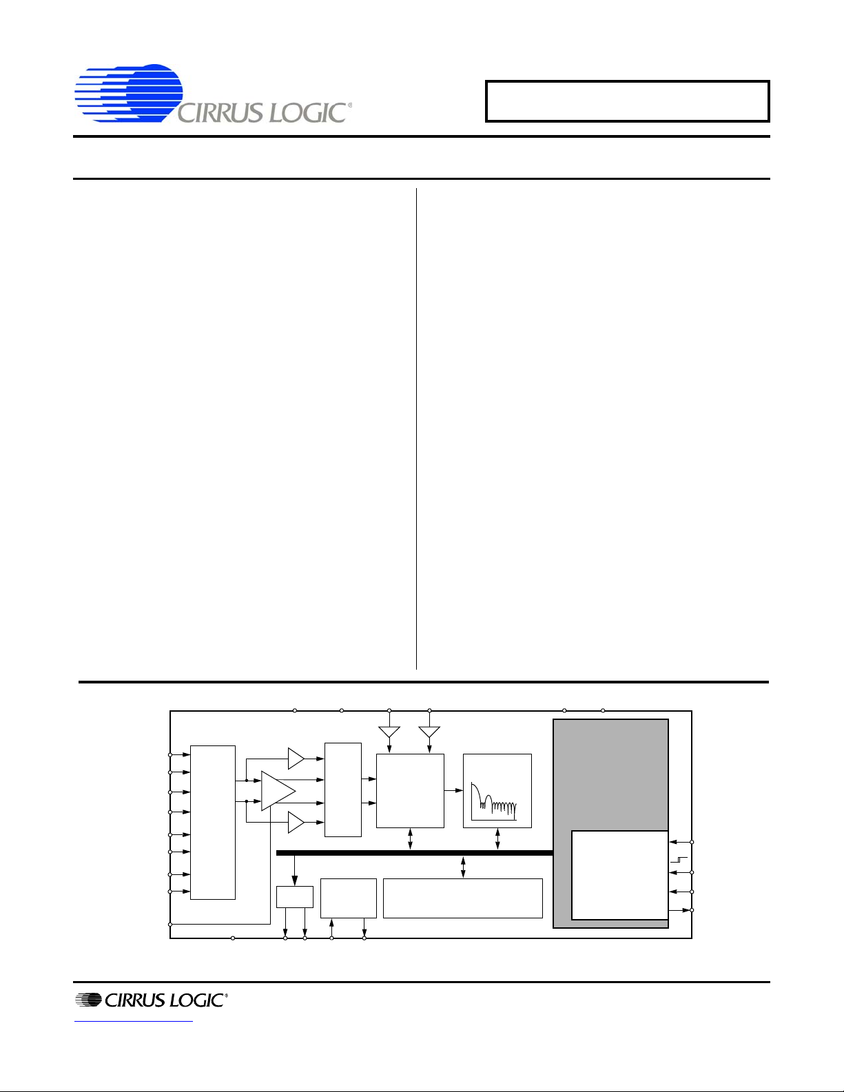
VA+ AGND VREF+ VREF- VD+DGND
XIN XOUT
NBV
Latch
Differential
Digital Filter
4th Order
ΔΣ
Modulator
Clock
Gen.
MUX
AIN2+
X1
X1
X1
CS5524
Shown
AIN2-
AIN1+
AIN1-
AIN4+
AIN4-
AIN3+
AIN3-
A0 A1CPD
Controller,
Programmable
Gain
Setup Registers,
&
Data FIFO &
Calibration R eg ist er s
Channel Scan
Logic
Serial Port
Interface
+
X20
SDO
SDI
SCLK
CS
CS5521/22/23/24/28
16-bit or 24-bit, 2/4/8-channel ADCs with PGIA
Features
Low Input Current (100 pA), Chopper-
stabilized Instrumentation Amplifier
Scalable Input Span (Bipolar/Unipolar)
- 2.5V VREF: 25 mV, 55 mV, 100 mV, 1 V,
2.5 V, 5 V
- External: 10 V, 100 V
Wide V
Fourth Order Delta-Sigma A/D Converter
Easy to Use Three-wire Serial Interface Port
- Programmable/Auto Channel Sequencer with
Conversion Data FIFO
- Accessible Calibration Registers per Channel
- Compatible with SPI™
System and Self Calibration
Eight Selectable Word Rates
- Up to 617 Sps (XIN = 200 kHz)
- Single Conversion Settling
- 50/60 Hz ±3 Hz Simultaneous Rejection
Single +5 V Power Supply Operation
- Charge Pump Drive for Negative Supply
- +3 to +5 V Digital Supply Operation
Low Power Consumption: 6.0 mW
Input Range (+1 to +5 V)
REF
and Microwire™
General Description
The CS5521/22/23/24/28 are highly integrated ΔΣ analog-to-digital converters (ADCs) which use chargebalance techniques to achieve 16-bit (CS5521/23) and
24-bit (CS5522/24/28) performance. The ADCs
either two-channel (CS5521/22), four-channel
(CS5523/24), or eight-channel (CS5528) devices and
include a low-input-current, chopper-stabilized instrumentation amplifier. To permit selectable input spans of
25 mV, 55 mV, 100 mV, 1 V, 2.5 V, and 5 V, the ADCs
include a PGA (programmable gain amplifier). To accommodate ground-based thermocouple applications,
the devices include a charge pump drive which provides
a negative bias voltage to the on-chip amplifiers.
These devices also include a fourth-order ΔΣ modulator
followed by a digital filter
output word rates
. The digital filters are designed to settle
which provides eight selectable
to full accuracy within one conversion cycle and when
operated at word rates below 30 Sps, they reject both
50 Hz and 60 Hz interference.
These single-supply products are ideal solutions for
measuring isolated and non-isolated, low-level signals in
process control applications.
ORDERING INFORMATION
See page 53.
come as
http://www.cirrus.com
Copyright Cirrus Logic, Inc. 2009
(All Rights Reserved)
JUL ‘09
DS317F8

TABLE OF CONTENTS
ANALOG CHARACTERISTICS................................................................................................5
TYPICAL RMS NOISE, CS5521/23.......................................................................................... 7
TYPICAL NOISE FREE RESOLUTION (BITS), CS5521/23 .................................................... 7
TYPICAL RMS NOISE, CS5522/24/28..................................................................................... 8
TYPICAL NOISE FREE RESOLUTION (BITS), CS5522/24/28 ............................................... 8
5 V DIGITAL CHARACTERISTICS...........................................................................................9
3 V DIGITAL CHARACTERISTICS...........................................................................................9
DYNAMIC CHARACTERISTICS ............................................................................................ 10
RECOMMENDED OPERATING CONDITIONS .....................................................................10
ABSOLUTE MAXIMUM RATINGS .........................................................................................10
SWITCHING CHARACTERISTICS ........................................................................................ 11
1. GENERAL DESCRIPTION ..................................................................................................... 13
1.1 Analog Input ........ ....................................... ... ... ... .... ...................................... .... ... ... .........13
1.1.1 Instrumentation Amplifier .........................................................................................14
1.1.2 Coarse/Fine Charge Buffers ...................................... ... ... ... .... ... ... ... .... ... ... .........14
1.1.3 Analog Input Span Considerations ..........................................................................15
1.1.4 Measuring Voltages Higher than 5 V ..................................................................15
1.1.5 Voltage Reference ................................. .... ... ... ... .... ... ...................................... ... 16
1.2 Overview of ADC Register Structure and Operating Modes ............................................16
1.2.1 System Initialization ................................... ... ... ....................................... ... ... ... ... 18
1.2.2 Command Register Quick Reference ...................................... ......................... 19
1.2.3 Command Register Descriptions ........................................................................20
1.2.4 Serial Port Interface ...................................... ... ... ....................................... ... ... ... 25
1.2.5 Reading/Writing the Offset, Gain, and Configuration Registers ................. .........26
1.2.6 Reading/Writing the Channel-Setup Registers ................................................... 26
1.2.6.1 Latch Outputs ............ .... ... ... ... ....................................... ... .... ... ... .........28
1.2.6.2 Channel Select Bits ............................................................................. 28
1.2.6.3 Output Word Rate Selection ...............................................................28
1.2.6.4 Gain Bits ........... ....................................... ... ...................................... ... 28
1.2.6.5 Unipolar/Bipolar Bit .......................... ... .... ... ... ... ... .... ... ... ... ...................28
1.2.7 Configuration Register ......................................................................... ... ... ... ... ... 28
1.2.7.1 Chop Frequency Select ....................................................................... 28
1.2.7.2 Conversion/Calibration Control Bits .................................................... 28
1.2.7.3 Power Consumption Control Bits ........................................................28
1.2.7.4 Charge Pump Disable ...................................... ... .... ... ... ... .... ... ... ... ... ... 29
1.2.7.5 Reset System Control Bits ............................................... .... ... ... ... ... ... 29
1.2.7.6 Data Conversion Error Flags ............................................................... 29
1.3 Calibration . ... .... ... ... ... .... ... ... ....................................... ... ... .... ............................................ 31
1.3.1 Self Calibration ....................... ... .... ... ... ....................................... ... ... .... ...............31
1.3.2 System Calibration ........................................ ... ... .... ...................................... ... ... 32
1.3.3 Calibration Tips ............. ...................................... .... ... ... ...................................... 34
1.3.4 Limitations in Calibration Range .........................................................................34
1.4 Performing Conversions and Reading the Data Conversion FIFO .................................. 34
1.4.1 Conversion Protocol ............................................................................................ 35
1.4.1.1 Single, One-Setup Conversion ............................................................ 35
1.4.1.2 Repeated One-Setup Conversions without Wait ................................. 35
1.4.1.3 Repeated One-Setup Conversions with Wait ......................................36
1.4.1.4 Single, Multiple-Setup Conversions ....................................................36
1.4.1.5 Repeated Multiple-Setup Conversions without Wait ...........................37
1.4.1.6 Repeated Multiple-Setup Conversions with Wait ................................37
1.4.2 Calibration Protocol ....................... ... ... ... .... ... ... ... ....................................... ... ... ... 38
CS5521/22/23/24/28
2 DS317F8

CS5521/22/23/24/28
1.4.3 Example of Using the CSRs to Perform Conversions and Calibrations .............. 38
1.5 Conversion Output Coding .............................................................................................. 40
1.5.1 Conversion Data FIFO Descriptions ................................................................... 41
1.6 Digital Filter ..................................................................................................................... 42
1.7 Clock Generator ........................... ... ... ... .... ... ....................................... ... ......................... 42
1.8 Power Supply Arrangements ................. .... ... ... ....................................... ... ... ................... 43
1.8.1 Charge Pump Drive Circuits ...................................... ... ... ... .... ............................ 45
1.9 Digital Gain Scaling ........................................................................................................ 45
1.10 Getting Started .............................................................................................................. 46
1.11 PCB Layout ................................................................................................................... 48
2. PIN DESCRIPTIONS .............................................................................................................. 49
2.1 Clock Generator ........................... ... ... ... .... ... ....................................... ... ......................... 50
2.2 Control Pins and Serial Data I/O ..................................................................................... 50
2.3 Measurement and Reference Inputs ............................................................................... 50
2.4 Power Supply Connections .......................... ... ... .... ... ... ....................................... ... ......... 51
3. SPECIFICATION DEFINITIONS ............................................................................................. 52
4. ORDERING INFORMATION .................................................................................................. 53
5. ENVIRONMENTAL, MANUFACTURING, & HANDLING INFORMATION ............................ 53
6. PACKAGE DIMENSION DRAWINGS .................................................................................... 54
7. REVISION HISTORY .............................................................................................................. 56
DS317F8 3

LIST OF FIGURES
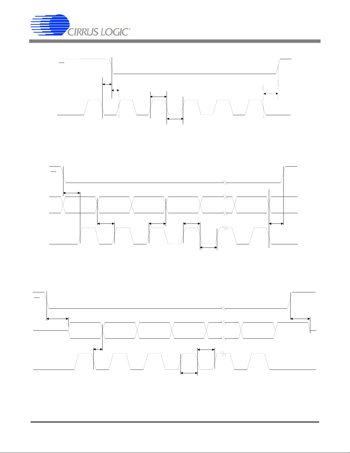
Figure 1. Continuous Running SCLK Timing (Not to Scale) ......................................................... 12
Figure 2. SDI Write Timing (Not to Scale).....................................................................................12
Figure 3. SDO Read Timing (Not to Scale)...................................................................................12
Figure 4. Multiplexer Configurations.............................................................................................. 13
Figure 5. Input Models for AIN+ and AIN- pins, ≤100 mV Input Ranges....................................... 14
Figure 6. Input Models for AIN+ and AIN- pins, >100 mV input ranges ........................................14
Figure 7. Input Ranges Greater than 5 V ......................................................................................16
Figure 8. Input Model for VREF+ and VREF- Pins........................................................................ 16
Figure 9. CS5523/24 Register Diagram........................................................................................17
Figure 10. Command and Data Word Timing................................................................................ 25
Figure 11. Self Calibration of Offset (Low Ranges)....................................................................... 32
Figure 12. Self Calibration of Offset (High Ranges)......................................................................32
Figure 13. Self Calibration of Gain (All Ranges) ...........................................................................32
Figure 14. System Calibration of Offset (Low Ranges)................................................................. 32
Figure 15. System Calibration of Offset (High Ranges) ................................................................33
Figure 16. System Calibration of Gain (Low Ranges)...................................................................33
Figure 17. System Calibration of Gain (High Ranges) ..................................................................33
Figure 18. Filter Response (Normalized to Output Word Rate = 15 Sps).....................................42
Figure 19. Typical Linearity Error for CS5521/23.......................................................................... 42
Figure 20. Typical Linearity Error for CS5522/24/28..................................................................... 42
Figure 21. CS5522 Configured to use on-chip charge pump to supply NBV ................................43
Figure 22. CS5522 Configured for ground-referenced Unipolar Signals.......................................44
Figure 23. CS5522 Configured for Single Supply Bridge Measurement....................................... 44
Figure 24. Charge Pump Drive Circuit for VD+ = 3 V.................................................................... 45
Figure 25. Alternate NBV Circuits .................................................................................................45
CS5521/22/23/24/28
LIST OF TABLES
Table 1. Relationship between Full Scale Input, Gain Factors, and Internal Analog
Signal Limitations .............................................................................................................15
Table 2. Command Register Quick Reference.............................................................................. 19
Table 3. Channel-Setup Registers................................................................................................27
Table 4. Configuration Register.....................................................................................................30
Table 5. Offset and Gain Registers...............................................................................................31
Table 6. Output Coding for 16-bit CS5521/23 and 24-bit CS5522/24/28......................................40
4 DS317F8
CHARACTERISTICS AND SPECIFICATIONS
CS5521/22/23/24/28
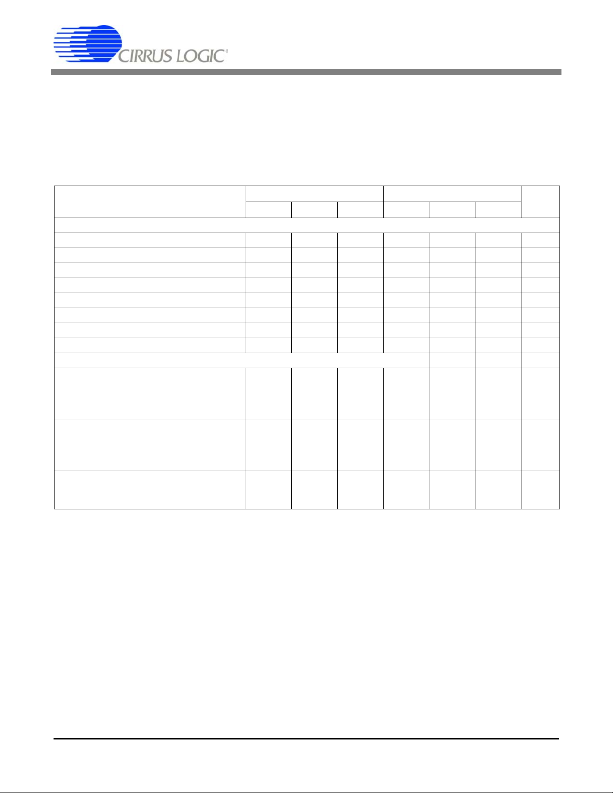
ANALOG CHARACTERISTICS (T
= 25° C; VA+, VD+ = 5 V ±5%; VREF+ = 2.5 V, VREF- = AGND,
A
NBV = -2.1 V, XIN = 32.768 kHz, CFS1-CFS0 = ‘00’, OWR (Output Word Rate) = 15 Sps, Bipolar Mode, Input
Range = ±100 mV; See Notes 1 and 2.)
CS5521/23 CS5522/24/28
Parameter
UnitMin Typ Max Min Typ Max
Accuracy
Resolution - - 16 - - 24 Bits
Linearity Error - ±0.0015 ±0.003 - ±0.0007 ±0.0015 %FS
Bipolar Offset (Note 3) - ±1±2 -±16 ±32 LSB
Unipolar Offset (Note 3) - ±2 ±4-±32 ±64 LSB
Offset Drift (Notes 3 and 4) - 20 - - 20 - nV/°C
Bipolar Gain Error - ±8 ±31 - ±8 ±31 ppm
Unipolar Gain Error - ±16 ±62 - ±16 ±62 ppm
Gain Drift (Note 4) - 1 3 - 1 3 ppm/°C
Power Supplies
Power Supply Currents (Normal Mode)
(Note 5)I
I
I
A+
D+
NBV
-
-
-
1.2
110
400
1.6
150
570
-
-
-
1.5
110
525
2.1
150
700
mA
µA
µA
Power Consumption (Note 6)
Normal Mode
Low Power Mode
Sleep
-
N/A
-
7.0
N/A
500
10
N/A
-
-
-
-
10.1
5.5
500
14.8
7.5
-
mW
mW
µW
Power Supply Rejection
Positive Supplies
dc NBV
-
-
120
110
-
-
-
-
120
110
-
-
dB
dB
N
N
Notes: 1. Applies after system calibration at any temperature within -40° C ~ +85° C.
2. Specifications guaranteed by design, characterization, and/or test.
3. Specif icatio n ap plie s to th e de vice on ly and does not inc l ud e an y eff ec ts by exte rn al pa ra sit ic
thermocouples. LSB
: N is 16 for the CS5521/23 and N is 24 for the CS5522/24/28
N
4. Drift over specified temperature range after calibration at power-up at 25° C.
5. Measured with Charge Pump Drive off.
6. All outputs unloaded. All input CMOS levels and the CS5521/23 do not have a low power mode.
DS317F8 5
CS5521/22/23/24/28
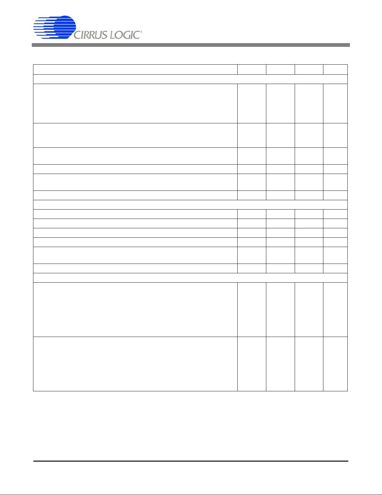
ANALOG CHARACTERISTICS (Continued)
Parameter Min Typ Max Unit
Analog Input
Common Mode + Signal on AIN+ or AIN- Bipolar/Unipolar Mode
NBV = -1.8 to -2.5 V Range = 25 mV, 55 mV, or 100 mV
Range = 1 V, 2.5 V, or 5 V
NBV = AGND Range = 25 mV, 55 mV, or 100 mV (Note 7)
Range = 1 V, 2.5 V, or 5 V
CVF Current on AIN+ or AIN- (Note 8)
Range = 25 mV, 55 mV, or 100 mV
Range = 1 V, 2.5 V, or 5 V
Input Current Drift (Note 8)
Range = 25 mV, 55 mV, or 100 mV - 1 - pA/°C
Input Leakage for Multiplexer when Off - 10 - pA
Common Mode Rejection dc
50, 60 Hz
Input Capacitance - 10 - pF
Voltage Reference Input
Range (VREF+) - (VREF-) 1 2.5 VA+ V
VREF+
VREF- NBV CVF Current (Note 8) - 5.0 - nA
Common Mode Rejection dc
50, 60 Hz
Input Capacitance - 16 - pF
System Calibration Specifications
Full Scale Calibration Range (VREF = 2.5V) Bipolar/Unipolar Mode
25 mV
55 mV
100 mV
1 V
2.5 V
5 V
Offset Calibration Range Bipolar/Unipolar Mode
25 mV
55 mV
100 mV (Note 9)
1 V
2.5 V
5 V
-0.150
NBV
1.85
0.0
-
-
-
-
(VREF-)+1
-
-
10
25
40
0.40
1.0
2.0
-
-
-
-
-
-
-
-
-
-
100
10
120
120
-VA+V
110
130
-
-
-
-
-
-
-
-
-
-
-
-
0.950
VA+
2.65
VA+
300
-
-
-
(VREF+)-1
-
-
32.5
71.5
105
1.30
3.25
VA+
±12.5
±27.5
±50
±0.5
±1.25
±2.50
pA
nA
dB
dB
dB
dB
mV
mV
mV
mV
mV
mV
V
V
V
V
V
V
V
V
V
V
V
Notes: 7. For the CS5528, the 25 mV, 55 mV and 100 mV ranges cannot be used unless NBV is powered at -1.8
to -2.5 V
8. See the section of the data sheet which discusses input models. Chop clock is 256 Hz (XIN/128) for
PGIA (programmable gain instrumentation amplifier). XIN = 32.768 kHz.
9. The maximum full scale signal can be limited by saturation of circuitry within the internal signal path.
6 DS317F8

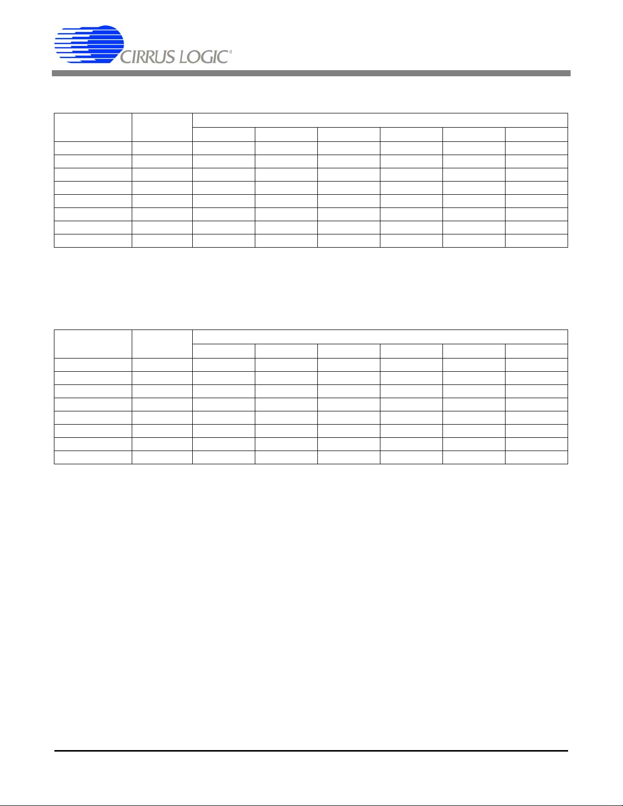
TYPICAL RMS NOISE, CS5521/23 (Notes 10 and 11)
CS5521/22/23/24/28
Output Rate
(Sps)
1.88 1.64 90 nV 148 nV 220 nV 1.8 µV 3.9 µV 7.8 µV
3.76 3.27 122 nV 182 nV 310 nV 2.6 µV 5.7 µV 11.3 µV
7.51 6.55 180 nV 267 nV 435 nV 3.7 µV 8.5 µV 18.1 µV
15.0 12.7 280 nV 440 nV 810 nV 5.7 µV 14 µV 28 µV
30.0 25.4 580 nV 1.1 µV 2.1 µV 18.2 µV 48 µV 96 µV
61.6 (Note 12) 50.4 2.6 µV 4.9 µV 8.5 µV 92 µV 238 µV 390 µV
84.5 (Note 12) 70.7 11 µV 27 µV 43 µV 458 µV 1.1 mV 2.4 mV
101.1 (Note 12) 84.6 41 µV 72 µV 130 µV 1.2 mV 3.4 mV 6.7 mV
Notes: 10. Wideband noise aliased into the baseband. Referred to the input. Typical values shown for 25° C.
11. To estimate Peak-to-Peak Noise, multiply RMS noise by 6.6 for all ranges and output rates.
12. For input ranges <100 mV and output rates ≥60 Sps, 16.384 kHz chopping frequency is used.
-3 dB Filter
Frequency
25 mV 55 mV 100 mV 1 V 2.5 V 5 V
Input Range, (Bipolar/Unipolar Mode)
TYPICAL NOISE FREE RESOLUTION (BITS), CS5521/23 (Note 13)
Output Rate
(Sps)
1.88 1.64 16 16 16 16 16 16
3.76 3.27 16 16 16 16 16 16
7.51 6.55 15 16 16 16 16 16
15.0 12.7 15 15 15 16 16 16
30.0 25.4 14 14 14 14 14 14
61.6 (Note 12) 50.4 12 12 12 12 12 12
84.5 (Note 12)70.7999999
101.1 (Note 12)84.6888888
-3 dB Filter
Frequency
25 mV 55 mV 100 mV 1 V 2.5 V 5 V
Input Range, (Bipolar Mode)
Notes: 13. For bipolar mode, the number of bits of Noise Free Resolution is LOG((2XInput Range)/(6.6xRMS
Noise))/LOG(2) rounded to the nearest bit. For unipolar mode, the number of bits of Noise Free
Resolution is LOG((Input Range)/(6.6xRMS Noise))/LOG(2) rounded to the nearest bit. Also, the
CS5521/23’s output conversions are 16 bits. Noise free Resolution numbers are based upon
VREF = 2.5 V and XIN = 32.768 kHz. The values will be affected directly by changes in VREF, but the
effects due to changes in the XIN frequency will be minor.
DS317F8 7
TYPICAL RMS NOISE, CS5522/24/28 (Notes 14 and 15)
CS5521/22/23/24/28
Output Rate
(Sps)
1.88 1.64 90 nV 95 nV 140 nV 1.5 µV 3 µV 6 µV
3.76 3.27 110 nV 130 nV 190 nV 2 µV 4 µV 8 µV
7.51 6.55 170 nV 200 nV 275 nV 2.5 µV 6 µV 11.5 µV
15.0 12.7 250 nV 330 nV 580 nV 4.5 µV 10 µV 20 µV
30.0 25.4 500 nV 1 µV 1.5 µV 16 µV 45 µV 85 µV
61.6 (Note 16) 50.4 2 µV 4 µV 8 µV 72 µV 195 µV 350 µV
84.5 (Note 16) 70.7 10 µV 20 µV 35 µV 340 µV 900 µV 2 mV
101.1 (Note 16) 84.6 30 µV 60 µV 105 µV 1.1 mV 3 mV 5.3 mV
Notes: 14. Wideband noise aliased into the baseband. Referred to the input. Typical values shown for 25° C.
15. To estimate Peak-to-Peak Noise, multiply RMS noise by 6.6 for all ranges and output rates.
16. For input ranges <100 mV and output rates ≥60 Sps, 16.384 kHz chopping frequency is used.
-3 dB Filter
Frequency
25 mV 55 mV 100 mV 1 V 2.5 V 5 V
Input Range, (Bipolar/Unipolar Mode)
TYPICAL NOISE FREE RESOLUTION (BITS), CS5522/24/28 (Note 17)
Output Rate
(Sps)
1.88 1.64 16 17 18 18 18 18
3.76 3.27 16 17 17 17 18 18
7.51 6.55 15 16 17 17 17 17
15.0 12.7 15 16 16 16 16 16
30.0 25.4 14 14 14 14 14 14
61.6 (Note 16) 50.4 12 12 12 12 12 12
84.5 (Note 16) 70.7 10 10 10 10 10 10
101.1 (Note 16)84.6888888
-3 dB Filter
Frequency
25 mV 55 mV 100 mV 1 V 2.5 V 5 V
Input Range, (Bipolar Mode)
Notes: 17. For bipolar mode, the number of bits of Noise Free Resolution is LOG((2XInput Range)/(6.6xRMS
Noise))/LOG(2) rounded to the nearest bit. For unipolar mode, the number of bits of Noise Free
Resolution is LOG((Input Range)/(6.6xRMS Noise))/LOG(2) rounded to the nearest bit. Also, the
CS5522/24/28’s output conversions are 24 bits. Noise free Resolution numbers are based upon
VREF = 2.5 V and XIN = 32.768 kHz. The values will be affected directly by changes in VREF, but the
effects due to changes in the XIN frequency will be minor.
8 DS317F8
CS5521/22/23/24/28
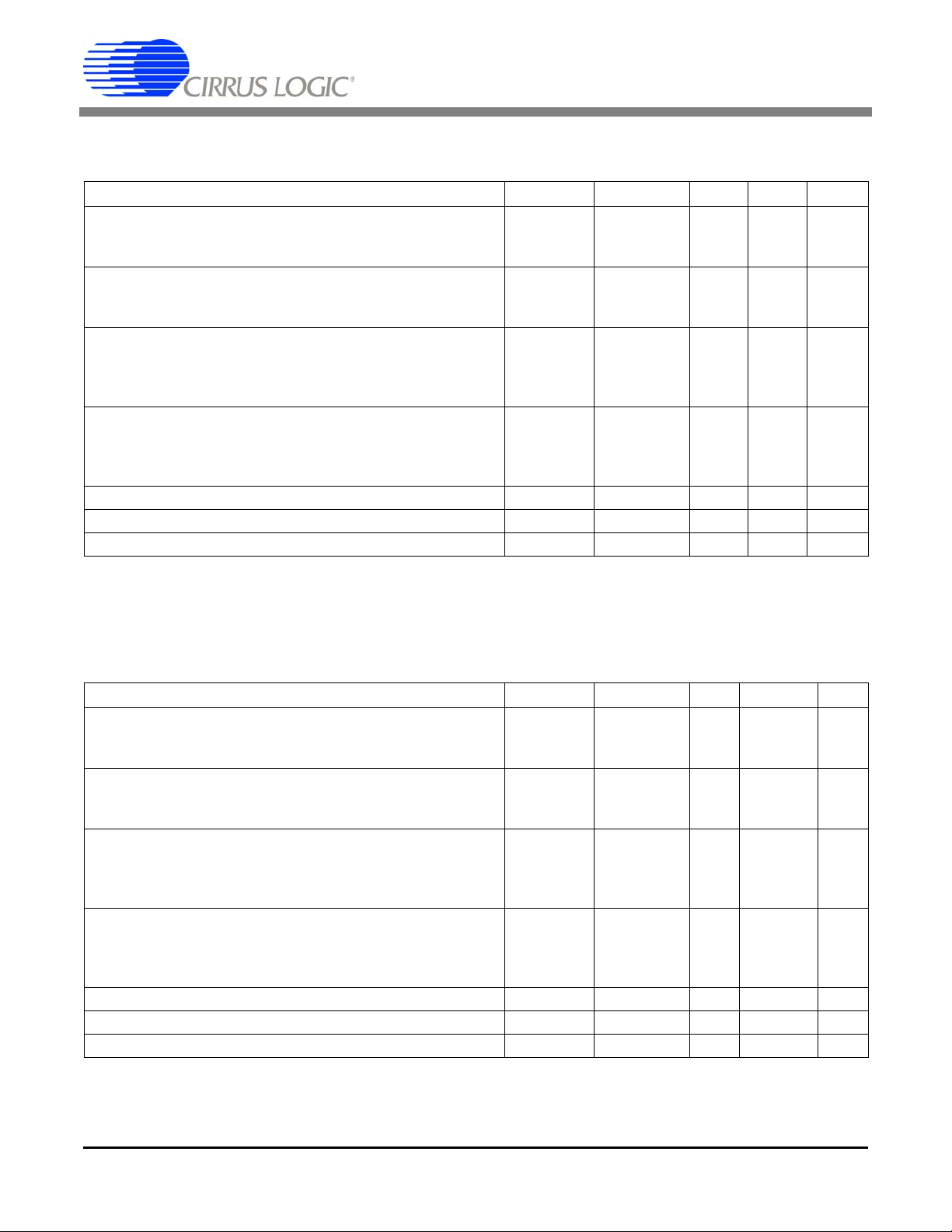
5 V DIGITAL CHARACTERISTICS (T
= 25° C; VA+, VD+ = 5 V ±5%; GND = 0;
A
See Notes 2 and 18.))
Parameter Symbol Min Typ Max Unit
High-level Input Voltage All Pins Except XIN and SCLK
XIN
SCLK
Low-level Input Voltage All Pins Except XIN and SCLK
XIN
SCLK
High-level Output Voltage
All Pins Except CPD and SDO (Note 19)
CPD, I
SDO, I
= -4.0 mA
out
= -5.0 mA
out
Low-level Output Voltage
All Pins Except CPD and SDO, I
CPD, I
SDO, I
= 1.6 mA
out
= 2 mA
out
= 5.0 mA
out
Input Leakage Current I
3-state Leakage Current I
Digital Output Pin Capacitance C
Notes: 18. All measurements performed under static conditions.
19. I
= -100 µA unless stated otherwise. (VOH = 2.4 V @ I
out
V
IH
V
IL
V
OH
V
OL
in
OZ
out
(VD+) - 0.45
= -40 µA.)
out
0.6 VD+
(VD+)-0.5
-
-
-
(VA+) - 1.0
(VD+) - 1.0
(VD+) - 1.0
-
-
-
-
-
-
-
-
-
-
-
-
-
-
-
-
-
-
0.8
1.5
0.6
-
-
-
0.4
0.4
0.4
V
V
V
V
V
V
V
V
V
V
V
V
-±1±10µA
--±10µA
-9-pF
3 V DIGITAL CHARACTERISTICS (T
= 25° C; VA+ = 5 V ±5%; VD+ = 3.0 V ±10%; GND = 0;
A
See Notes 2 and 18.)
Parameter Symbol Min Typ Max Unit
High-level Input Voltage All Pins Except XIN and SCLK
XIN
SCLK
Low-level Input Voltage All Pins Except XIN and SCLK
XIN
SCLK
High-level Output Voltage
All Pins Except CPD and SDO, I
CPD, I
SDO, I
= -400 µA
out
= -4.0 mA
out
= -5.0 mA
out
Low-level Output Voltage
All Pins Except CPD and SDO, I
CPD, I
SDO, I
= 400 µA
out
= 2 mA
out
= 5.0 mA
out
Input Leakage Current I
3-state Leakage Current I
Digital Output Pin Capacitance C
V
IH
V
IL
V
OH
V
OL
in
OZ
out
0.6 VD+
(VD+)-0.5
(VD+) - 0.45
-
-
-
(VA+) - 0.3
(VD+) - 1.0
(VD+) - 1.0
-
-
-
-
-
-
-
-
-
-
-
-
-
-
-
-
-
-
0.16 VD+
0.3
0.6
-
-
-
0.3
0.4
0.4
-±1±10µA
--±10µA
-9-pF
V
V
V
V
V
V
V
V
V
V
V
V
DS317F8 9
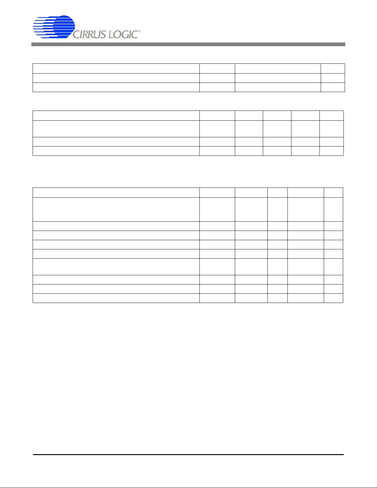
DYNAMIC CHARACTERISTICS
Parameter Symbol Ratio Unit
Modulator Sampling Frequency f
Filter Settling Time to 1/2 LSB (Full-scale Step) t
CS5521/22/23/24/28
s
s
XIN/4 Hz
1/f
out
s
RECOMMENDED OPERATING CONDITIONS
(AGND, DGND = 0 V; See Note 20.)
Parameter Symbol Min Typ Max Unit
DC Power Supplies Positive Digital
Positive Analog
Analog Reference Voltage (VREF+) - (VREF-) VRef
VD+
VA+
diff
2.7
4.75
5.0
5.0
5.25
5.25
1.0 2.5 VA+ V
V
V
Negative Bias Voltage NBV -1.8 -2.1 -2.5 V
Notes: 20. All voltages with respect to ground.
ABSOLUTE MAXIMUM RATINGS (AGND, DGND = 0 V; See Note 20.)
Parameter Symbol Min Typ Max Unit
DC Power Supplies (Note 21)
Positive Digital
Positive Analog
Negative Bias Voltage Negative Potential NBV +0.3 -2.1 -3.0 V
Input Current, Any Pin Except Supplies (Note 22 and 23) I
Output Current I
Power Dissipation (Note 24) PDN - - 500 mW
Analog Input Voltage VREF pins
AIN Pins
Digital Input Voltage V
Ambient Operating Temperature T
Storage Temperature T
VD+
VA+
IN
OUT
V
INR
V
INA
IND
A
stg
-0.3
-0.3
-
-
+6.0
+6.0
V
V
--±10mA
--±25mA
NBV -0.3
NBV -0.3
--(VA+) + 0.3
(VA+) + 0.3VV
-0.3 - (VD+) + 0.3 V
-40 - 85 °C
-65 - 150 °C
Notes: 21. No pin should go more negative than NBV - 0.3 V.
22. Applies to all pins including continuous overvoltage conditions at the analog input (AIN) pins.
23. Transient current of up to 100 mA will not cause SCR latch-up. Maximum input current for a power
supply pin is ±50 mA.
24. Total power dissipation, including all input currents and output currents.
WARNING: Operation at or beyond these limits may result in permanent damage to the device.
Normal operation is not guaranteed at these extremes.
10 DS317F8
CS5521/22/23/24/28
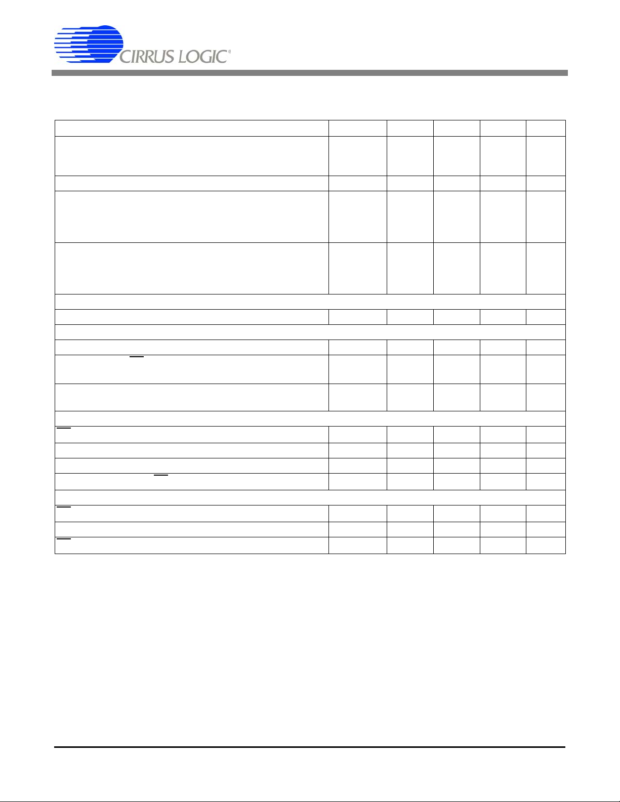
SWITCHING CHARACTERISTICS (T
Levels: Logic 0 = 0 V, Logic 1 = VD+; C
= 50 pF.))
L
= 25° C; VA+ = 5 V ±5%; VD+ = 3.0 V ±10% or 5 V ±5%;
A
Parameter Symbol Min Typ Max Unit
Master Clock Frequency (Note 25)
External Clock or Internal Oscillator (CS5522/24/28)
(CS5521/23)
XIN
30
30
32.768
32.768
200
130
kHz
kHz
Master Clock Duty Cycle 40 - 60 %
Rise Times (Note 26)
Any Digital Input Except SCLK
SCLK
Any Digital Output
Fall Times (Note 26)
Any Digital Input Except SCLK
SCLK
Any Digital Output
t
rise
t
fall
-
-
-
-
-
-
50
50
-
-
-
-
1.0
100
-
1.0
100
-
µs
µs
ns
µs
µs
ns
Start-up
Oscillator Start-up Time XTAL = 32.768 kHz (Note 27) t
ost
-500-ms
Serial Port Timing
Serial Clock Frequency SCLK 0 - 2 MHz
SCLK Falling to CS
Falling for continuous running SCLK
t
0
100 - - ns
(Note 28)
Serial Clock Pulse Width High
Pulse Width Low
t
1
t
2
250
250
-
-
-
-
ns
ns
SDI Write Timing
CS
Enable to Valid Latch Clock t
Data Set-up Time prior to SCLK rising t
Data Hold Time After SCLK Rising t
SCLK Falling Prior to CS
Disable t
3
4
5
6
50 - - ns
50 - - ns
100 - - ns
100 - - ns
SDO Read Timing
CS
to Data Valid t
SCLK Falling to New Data Bit t
CS
Rising to SDO Hi-Z t
7
8
9
--150ns
--150ns
--150ns
Notes: 25. Device parameters are specified with a 32.768 kHz clock; however, clocks up to 200 kHz
(CS5522/24/28) or 130 kHz (CS5521/23) can be used for increased throughput.
26. Specified using 10% and 90% points on waveform of interest. Output loaded with 50 pF.
27. Oscillator start-up time varies with crystal parameters. This specification does not apply when using an
external clock source.
28. Applicable when SCLK is continuously running.
Specifications are subject to change without notice.
DS317F8 11
CS5521/22/23/24/28
CS
SCLK
t
0
t
2
t
1
t
3
t
6
Figure 1. Continuous Running SCLK Timing (Not to Scale)
CS
SCLK
MSB
MSB-1 LSBSDI
t
3
t
4
t
5
t
1
t
2
t
6
Figure 2. SDI Write Timing (Not to Scale)
CS
SCLK
MSB
MSB-1 LSB
SDO
t
7
t
8
t
1
t
2
t
9
Figure 3. SDO Read Timing (Not to Scale)
12 DS317F8

1. GENERAL DESCRIPTION
VREF+
Differential
4th
order
delta-
sigma
modulator
Digital
Filter
Programmable
Gain
VREF-
NBV
X20
M
U
X
AIN2+
AIN2-
AIN1+
AIN1-
CS5522
IN+
IN-
AIN4+
AIN4-
*
*
*
AIN1+
AIN1-
CS5524
AIN8+
AIN7+
*
*
*
AIN1+
CS5528
M
U
X
M
U
X
IN+
IN-
IN+
IN-
IN+
IN-
Figure 4. Multiplexer Configurations
NBV also supplies the negative
supply voltage for the coarse/fine
change buffers
CS5521/22/23/24/28
The CS5521/22/23/24/28 are highly integrated ΔΣ
Analog-to-Digital Converters (ADCs) which use
charge-balance techniques to achieve 16-bit
(CS5521/23) and 24-bit (CS5522/24/28) performance. The ADCs come as either two-channel
(CS5521/22), four-channel (CS5523/24), or eightchannel (CS5528) devices, and include a low input
current, chopper-stabilized instrumentation amplifier. To permit selectable input spans of 25 mV,
55 mV, 100 mV, 1 V, 2.5 V, and 5 V, the ADCs include a PGA (programmable gain amplifier). To
accommodate ground-based thermocouple applications, the devices include a CPD (Charge Pump
Drive) which provides a negative bias voltage to
the on-chip amplifiers.
These devices also include a fourth order DS modulator followed by a digital filter
eight selectable output word rates of
which provides
1.88 Sps,
3.76 Sps, 7.51 Sps, 15 Sps, 30 Sps, 61.6 Sps,
84.5 Sps, and 101.1 Sps
(XIN = 32.768 kHz).
The
devices are capable of producing output update
rates up to 617 Sps when a 200 kHz clock is used
(CS5522/24/28) or up to 401 Sps using a 130 kHz
clock (CS5521/23). Further note that the digital fil-
ters are designed to settle to full accuracy within
one conversion cycle and simultaneously reject
both 50 Hz and 60 Hz interference when operated
at word rates below 30 Sps (assuming a XIN clock
frequency of 32.768 kHz).
To ease communication between the ADCs and a
micro-controller, the converters include an easy to
use three-wire serial interface which is SPI™ and
Microwire™ compatible.
1.1 Analog Input
Figure 4 illustrates a block diagram of the analog input signal path inside the CS5521/22/23/24/28. The
front end consists of a multiplexer (break before
make configuration), a chopper-stabilized instrumentation amplifier with fixed gain of 20X,
coarse/fine charge buffers, and a programmable gain
section. For the 25 mV, 55 mV, and 100 mV input
ranges, the input signals are amplified by the 20X instrume ntati on amp lifi er. For the 1 V, 2.5 V, and 5 V
input ranges, the instrumentation amplifier is bypassed and the input signals are connected to the
Programmable Gain block via coarse/fine charge
buffers.
DS317F8 13
CS5521/22/23/24/28
AIN
25 m V, 55 mV, and 100 mV Ranges
C=48pF
CFS1/CFS0 = 00, f = 256 Hz
CFS1/CFS0 = 01, f = 4096 Hz
CFS 1/CFS0 = 10, f = 16.384 kHz
CFS1/CFS0 = 11, f = 1024 Hz
V≤25 mV
i=fV C
os
osn
Figure 5. Input Models for AIN+ and AIN- pins, ≤100
mV Input Ranges
AIN
C=20pF
f=32.768kHz
φ
Coarse
1
φ
Fine
1
V≤25 mV
i=fV C
os
osn
1 V, 2.5 V and 5 V Ranges
Figure 6. Input Models for AIN+ and AIN- pins, >100
mV input ranges
,
1.1.1 Instrumentation Amplifier
The instrumentation amplifier is chopper stabilized
and is activated any time conversions are performed
with the low-level input ranges, ≤100 mV. The amplifier is powered from VA+ and from the NBV
(Negative Bias Voltage) pin allowing the
CS5521/22/23/24/28 to be operated in either of two
analog input configurations. The NBV pin can be biased to a negative voltage between -1.8 V and
-2.5 V, or tied to AGND (for the CS5528, NBV has
to be between -1.8 V and -2.5 V for the ranges below
100 mV when the amplifier is engaged). The common-mode-plus-signal range of the instrumentation
amplifier is 1.85 V to 2.65 V with NBV grounded.
The common-mode-plus-signal range of the instrumentation amplifier is -0.150 V to 0.950 V with
NBV between -1.8 V to -2.5 V. Whether NBV is
tied between -1.8 V and -2.5 V or tied to AGND,
the (Common Mode + Signal) input on AIN+ and
AIN- must stay between NBV and VA+.
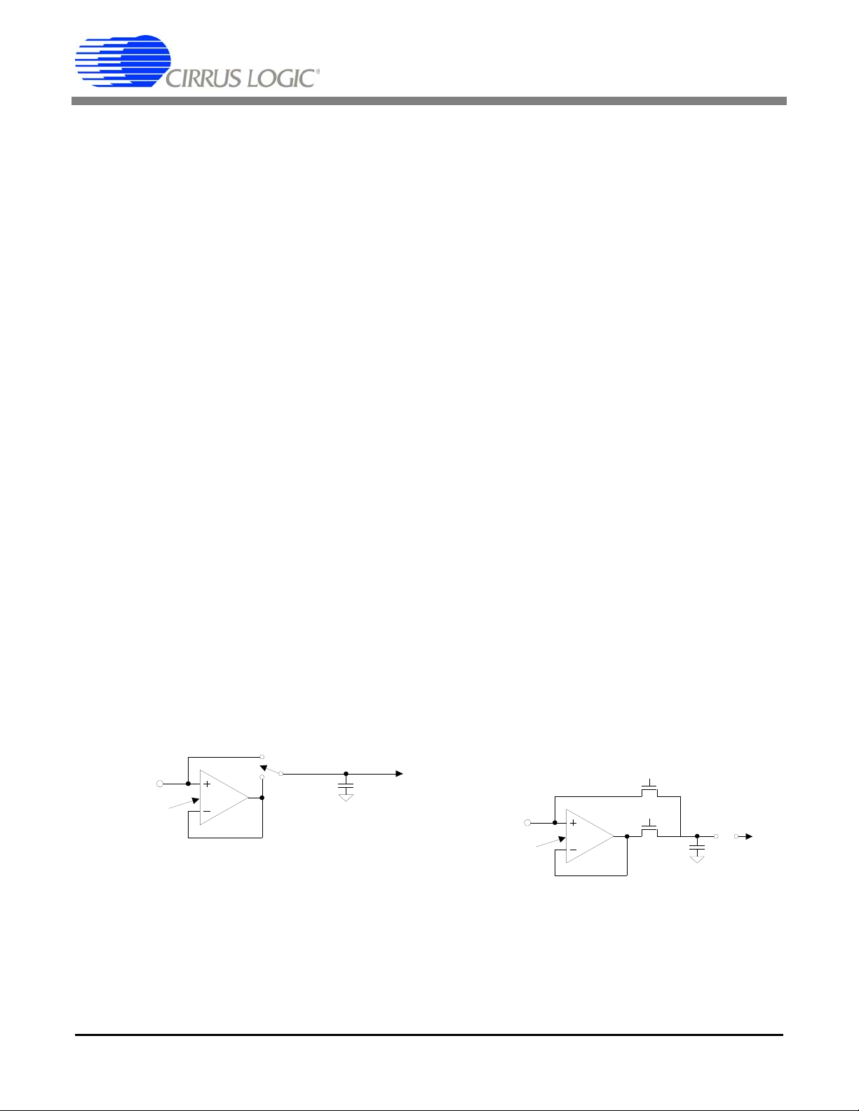
Figure 5 illustrates an analog input model for the
ADCs when the instrumentation amplifier is engaged. The CVF (sampling) input current for each
of the analog input pins depends on the CFS1 and
CFS0 (Chop Frequency Select) bits in the configuration register (see Configuration Register for details). Note that the CVF current is lowest with the
CFS bits in their default states (cleared to logic 0s).
Further note that the CVF current into the instrumentation amplifier is less than 300 pA over -40°C
to +85°C. Note that Figure 5 is for input current
modeling only. For physical input capacitance see
‘Input Capacitance’ specification under ANALOG
CHARACTERISTICS. Also refer to Applications
Note AN30 - “Switched-Capacitor A/D Converter
Input Structures” for more details on input models
and input sampling currents.
Note: Residual noise appears in the converter’s baseband for
output word rates greater than 61.6 Sps if the CFS bits
are logic 0 (chop clock = 256 Hz). For word rates of
30 Sps and lower, 256 Sps chopping is recommended,
and for 61.6 Sps, 84.5 Sps and 101.1 Sps word rate settings, 4096 Hz chopping is recommended.
1.1.2 Coarse/Fine Charge Buffers
The unity gain buffers are activated any time conversions are performed with the high-level inputs ranges, 1 V, 2.5 V, and 5 V. The u nity gai n bu ffer s ar e
designed to accommodate rail-to-rail input signals.
The common-mode-plus-signal range for the unity
gain buffer amplifier is NBV to VA+.
Typical CVF (sampling) current for the unity gain
buffer amplifiers is about 10 nA
(XIN = 32.768 kHz, see Figure 6).
14 DS317F8
CS5521/22/23/24/28
Note: 1. The converter's actual input range, the delta-sigma's nominal full-scale input, and the delta-sigm a's
maximum full-scale input all scale directly with the value of the voltage reference. The values in the
table assume a 2.5
V VREF voltage.
2. The 2.8 V limit at the output of the 20X amplifier is the differential output voltage.
Input Range
(1)
Max. Differential Output
20X Amplifier
VREF Gain Factor
Δ-Σ Nominal
(1)
Differential Input
Δ-Σ
(1)
Max. Input
± 25 mV
2.8 V
(2)
2.5V 5 ± 0.5 V ± 0.75 V
± 55 mV
2.8 V
(2)
2.5V 2.272727... ± 1.1 V ± 1.65 V
± 100 mV
2.8 V
(2)
2.5V 1.25 ± 2.0 V ± 3.0 V
± 1.0 V - 2.5V 2.5 ± 1.0 V ± 1.5 V
± 2.5 V - 2.5V 1.0 ± 2.5 V ± 5.0 V
± 5.0 V - 2.5V 0.5 ± 5.0 V 0V, VA+
Table 1. Relationship between Full Scale Input, Gain Factors, and Internal Analog
Signal Limitations
1.1.3 Analog Input Span Considerations
The CS5521/22/23/24/28 is designed to measure
full-scale ranges of 25 mV, 55 mV, 100 mV, 1 V,
2.5 V, and 5 V. Other full scale values can be accommodated by performing a system calibration
within the limits specified. See the Calibration section for more details. Another way to change the
full scale range is to increase or to decrease the
voltage reference to a voltage other than 2.5 . See
the Voltage Reference section for more details.
Three factors set the operating limits for the input
span. They include: instrumentation amplifier saturation, modulator 1’s density, and a lower reference
voltage. When the 25 mV, 55 mV, or 100 mV
range is selected, the input signal (including the
common-mode voltage and the amplifier offset
voltage) must not cause the 20X amplifier to saturate in either its input stage or output stage. To prevent saturation, the absolute voltages on AIN+ and
AIN- must stay within the limits specified (refer to
the Analog Input section). Additionally, the differential output voltage of the amplifier must not exceed 2.8 V. The equation
is the differential input voltage and VOS is the absolute maximum offset voltage for the instrumentation amplifier (VOS will not exceed 40 mV). If the
differential output voltage from the amplifier exceeds 2.8 V, the amplifier may saturate, which will
cause a measurement error.
The input voltage into the modulator must not
cause the modulator to exceed a low of 20 percent
or a high of 80 percent 1's density. The nominal
full-scale input span of the modulator (from 30 percent to 70 percent 1’s density) is determined by the
VREF voltage divided by the Gain Factor. See
Table 1 to determine if the CS5521/22/23/24/28 is
being used properly. For example, in the 55 mV
range, to determine the nominal input voltage to the
modulator, divide VREF (2.5 V) by the Gain Factor (2.2727).
When a smaller voltage reference is used, the resulting code widths are smaller causing the converter output codes to exhibit more changing codes
for a fixed amount of noise. Table 1 is based upon
a VREF = 2.5 V. For other values of VREF, the
values in Table 1 must be scaled accordingly.
ABS(VIN + VOS) x 20 = 2.8 V
defines the differential output limit, where
VIN = (AIN+) - (AIN-)
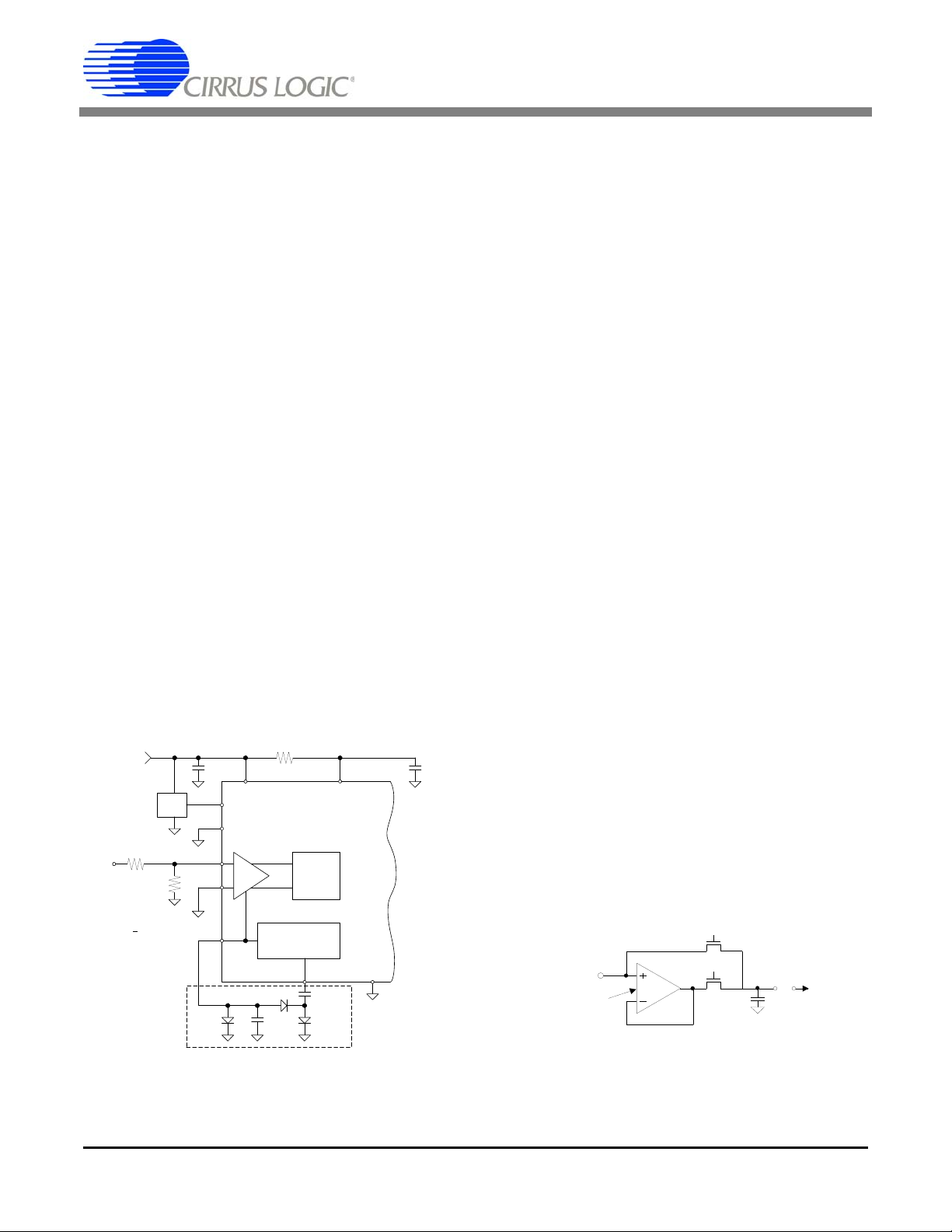
1.1.4 Measuring Voltages Higher than 5 V
Some systems require the measurement of voltages
greater than 5 V. The input current of the instru-
DS317F8 15
CS5521/22/23/24/28
Voltage
Divider
PGIA set for
+
100 mV
±10V
Charge Pump
Regulator
ΔΣ
ADC
PGIA
+5 V
2.5 V
VA+
VREF+
VREF-
VD+
+
-
NBV
V
≈
-2.1 V
+
10
μ
F
0.033
μ
F
CPD
0.1 μF
10
Ω
0.1 μF
1N4148
1N4148BAT85
Charge Pump
Circuitry
DGND
chop clock = 256 Hz
10 K
Ω
1 M
Ω
Figure 7. Input Ranges Greater than 5 V
VREF
C = 10pF
f = 32.768 kHz
2
φ
Fin e
1
V ≤ 25mV
i = fV C
os
osn
φ
Coarse
Figure 8. Input Model for VREF+ and VREF- Pins
mentation amplifier with a gain range setting of
100 mV or less, is typically 100 pA. This is low
enough to permit large external resistors to divide
down a large external signal without significant
loading. Figure 7 illustrates an example circuit. Refer to Application Note 158 for more details on
high-voltage (>5 V) measurement.
1.1.5 Voltage Reference
The CS5521/22/23/24/28 devices are specified for
operation with a 2.5 V reference voltage between
the VREF+ and VREF- pins of the device. For a
single-ended reference voltage, such as the
LT1019-2.5, the reference voltage is input into the
VREF+ pin of the converter and the VREF- pin is
grounded.
The differential voltage between the VREF+ and
VREF- can be any voltage from 1.0 V up to VA+,
however, the VREF+ cannot go above VA+ and the
VREF- pin can not go below NBV.
Figure 8 illustrates the input models for the VREF
pins. The dynamic input current for each of the pins
can be determined from the models shown.
1.2 Overview of ADC Register Structure and Operating Modes
The CS5521/22/23/24/28 ADCs have an on-chip
controller, which includes a number of user-accessible registers. The registers are used to hold offset
and gain calibration results, configure the chip's
operating modes, hold conversion instructions, and
to store conversion data words. Figure 9 depicts a
block diagram of the on-chip controller’s internal
registers for the CS5523/24.
Each of the converters has 24-bit registers to function as offset and gain calibration registers for each
channel. The converters with two channels have
two offset and two gain calibration registers, the
converters with four channels have four offset and
four gain calibration registers, and the eight channel converter has eight offset and eight gain calibration registers. These registers hold calibration
results. The contents of these registers can be read
or written by the user. This allows calibration data
to be off-loaded into an external EEPROM. The
user can also manipulate the contents of these registers to modify the offset or the gain slope of the
converter.
16 DS317F8
The converters include a 24-bit configuration register of which 17 of the bits are used for setting options such as the conversion mode, operating power
options, setting the chop clock rate of the instru-

CS5521/22/23/24/28
AIN1
AIN2
AIN3
AIN4
4 (24) 4 (24) 4 (12 x 2) 8 x 24
Off 1
Off 2
Off 3
Off 4
Gain 1
Gain 2
Gain 3
Gain 4
Setup 1
Setup 3
Setup 5
Setup 7
Setup 2
Setup 4
Setup 6
Setup 8
DATA
FIFO
SDO
1 x 24
Configuration
Chop Frequency
Multiple Conversions
Depth Pointer
Loop
Read Convert
Powerdown Modes
Flags
Etc.
Latch Outputs
Channel Select
Output Word Rate
PGA Selection
Unipolar/Bipolar
Figure 9. CS5523/24 Register Diagram
mentation amplifier, and providing a number of
flags which indicate converter operation.
A group of registers, called Channel Set-up Registers, are also included in the converters. These registers are used to hold pre-loaded conversion
instructions. Each channel set-up register is 24 bits
wide and holds two 12-bit conversion instructions
(Setups). Upon power-up, these registers can be
initialized by the user’s microcontroller with conversion instructions. The user can then use bits in
the configuration register to choose a conversion
mode.
Several conversion modes are possible. Using the
single conversion mode, an 8-bit command word
can be written into the serial port. The command includes pointer bits which ‘point’ to a 12-bit command in one of the Channel Setup Registers which
is to be executed. The 12-bit commands can be setup to perform a conversion on any of the input
channels of the converter. More than one of the 12bit Setups can be used for the same analog input
channel. This allows the user to convert on the
same signal with either a different conversion
speed, a different gain range, or any of the other options available in the Setup Register. The user can
set up the registers to perform conversions using
different conversion options on each of the input
channels.
The ADCs also include multiple-channel conversion capability. User bits in the configuration register of the ADCs can be configured to sequence
through the 12-bit command Setups, performing a
conversion according to the content of each 12-bit
Setup. This channel scanning capability can be
configured to run continuously, or to scan through
a specified number of Setup Registers and stop until commanded to continue. In the multiple-channel
scanning modes, the conversion data words are
loaded into an on-chip data FIFO. The converter issues a flag on the SDO pin when a scan cycle is
completed so the user can read the FIFO. More details are given in the following pages.
Instructions are provided on how to initialize the
converter, perform offset and gain calibrations, and
to configure the converter for the various conversion modes. Each of the bits of the configuration
register and of the Channel Setup Registers is described. A list of examples follows the description
section. Table 2 can be used to decode all valid
commands (the first 8 bits into the serial port).
DS317F8 17
 Loading...