

Page 1
CS5525
CS5526
16-bit/20-bit, Multi-range ADC with 4-bit Latch
Features
z Delta-sigma A/D Converter
- Linearity Error: 0.0015%FS
- Noise-free Resolution: 18-bits
z Bipolar/Unipolar Input Ranges
- 25 mV, 55 mV, 100 mV, 1 V, 2.5 V and 5 V
z Chopper Stabilized Instrumentation Amplifier
z On-chip Charge Pump Drive Circuitry
z 4-bit Output Latch
z Simple three-wire serial interface
- SPI™ and Microwire™ Compatible
- Schmitt Trigger on Serial Clock (SCLK)
z Programmable Output Word Rates
- 3.76 Sps to 202 Sps (XIN = 32.768 kHz)
- 11.47 Sps to 616 Sps (XIN = 100 kHz)
z Output Settles in One Conversion Cycle
z Simultaneous 50/60 Hz Noise Rejection
z System and Self-calibration with
Read/Write Registers
z Single +5 V Analog Supply
+3.0 V or +5 V Digital Supply
z Low-power Mode Consumption: 4.9 mW
- 1.8 mW in 1 V, 2.5 V, and 5 V Input Ranges
General Description
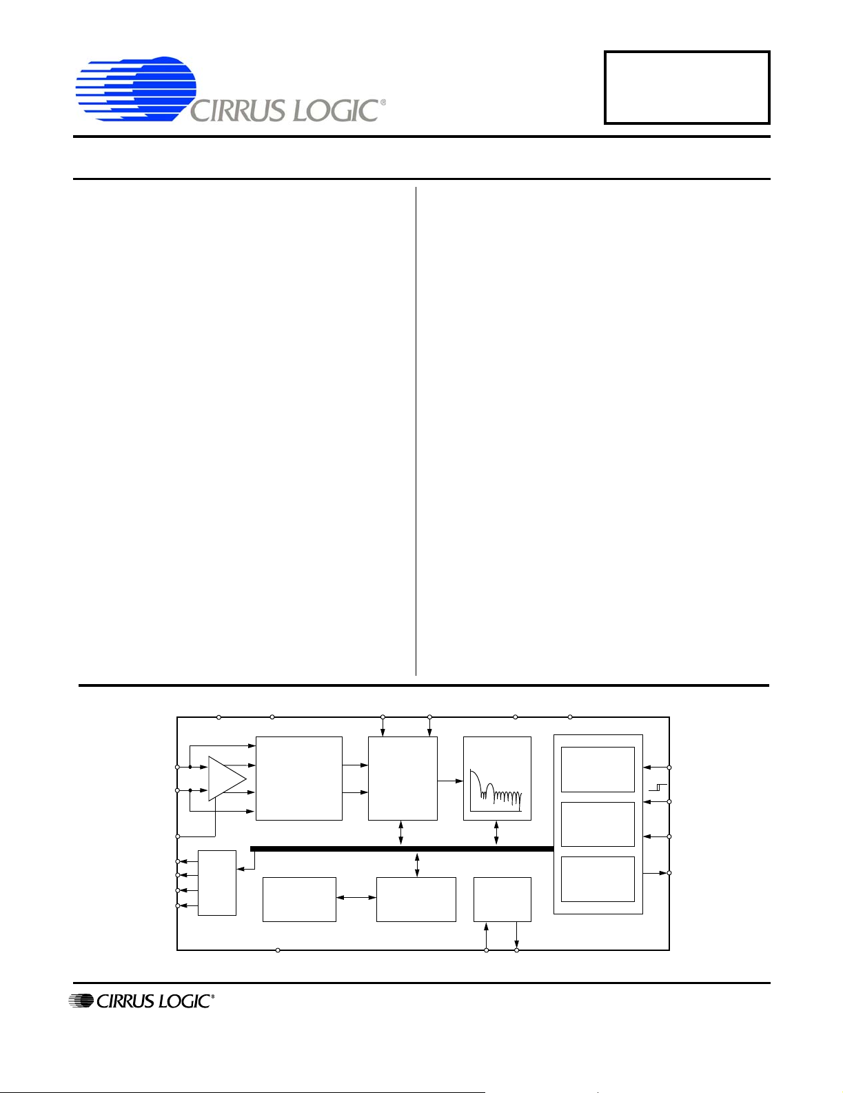
The 16-bit CS5525 and the 20-bit CS5526 are highly integrated ∆Σ A/D converters which include an
instrumentation amplifier, a PGA (programmable gain
amplifier), eight digital filters, and self and system calibration circuitry.
The converters are designed to provide their own negative supply which enables their on-chip instrumentation
amplifiers to measure bipolar ground-referenced signals
≤±100 mV. By directly supplying NBV with -2.5 V and
with VA+ at 5 V,
can be measured.
The digital filters provide programmable output update
rates between 3.76 Sps to 202 Sps (XIN = 32.768 kHz).
Output word rates can be increased by approximately 3X
by using XIN = 100 kHz. Each filter is designed to settle
to full accuracy for its output update rate in one conversion cycle. The filters with word rates of 15 Sps or less
(XIN = 32.768 kHz) reject both 50 and 60 Hz (
interference simultaneously.
Low power, single conversion settling time, programmable output rates, and the ability to handle negative input
signals make these single supply products ideal solutions for isolated and non-isolated applications.
ORDERING INFORMATION
See page 29.
±2.5 V signals (with respect to ground)
±3 Hz) line
AIN+
AIN-
NBV
A0
A1
A2
A3
http://www.cirrus.com
VA+ AGND VREF+ VREF- VD+DGND
+
X20
-
Latch
Programmable
Gain
Calibration
Memory
CPD
Differential
4th Order
Delta-Sigma
Modulator
Calibration µC
Copyright © Cirrus Logic, Inc. 2005
(All Rights Reserved)
Digital Filter
Clock
Gen.
XIN XOUT
Calibration
Register
Control
Register
Output
Register
CS
SCLK
SDI
SDO
AUG ‘05
DS202F5
Page 2
CS5525 CS5526
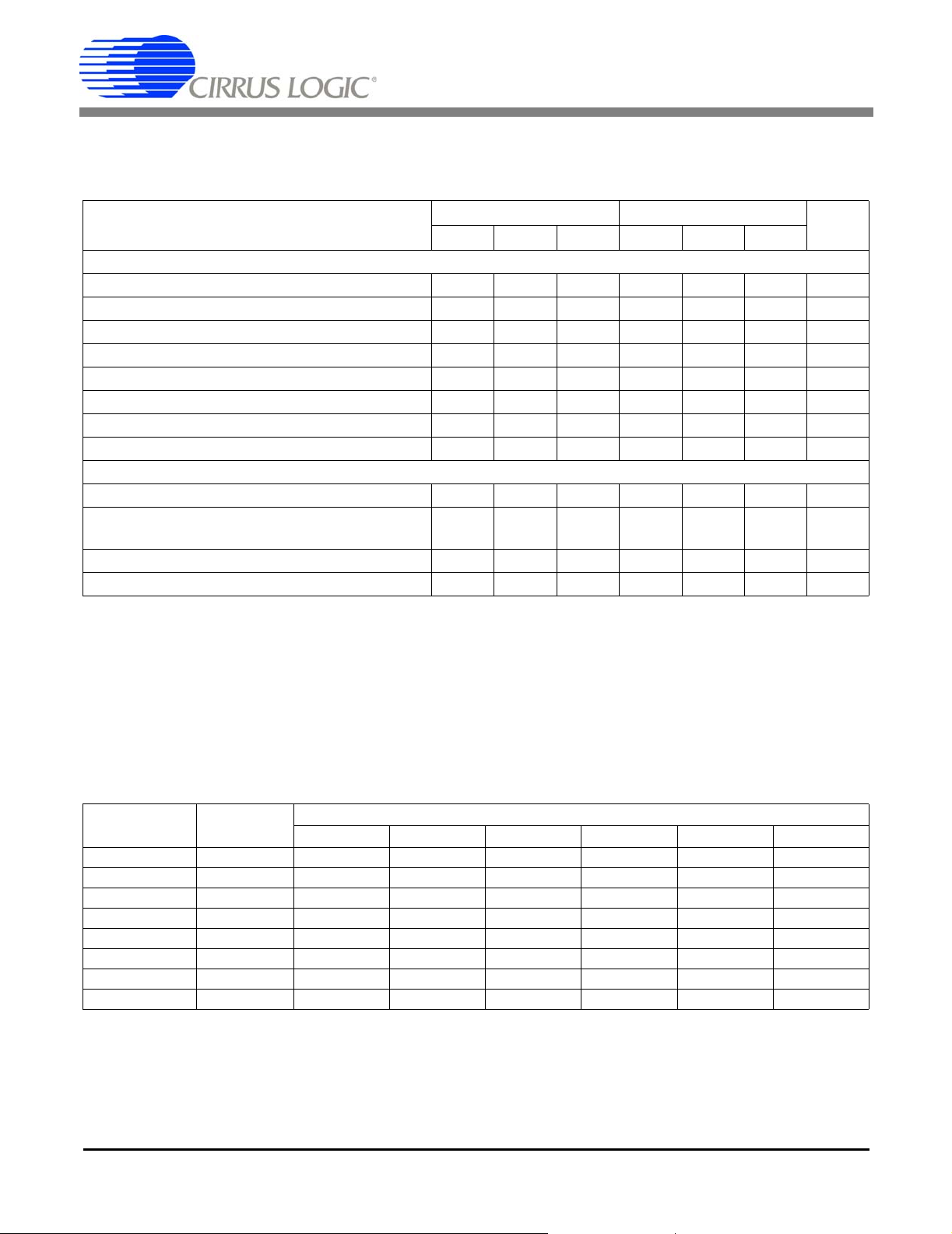
ANALOG CHARACTERISTICS (T
NBV = -2.1 V, FCLK = 32.768 kHz, OWR (Output Word Rate) = 15 Sps, Bipolar Mode, Input Range = ±100 mV;
See Notes 1 and 2.)
Parameter
Accuracy
Linearity Error - ±0.0015 ±0.003 - ±0.0007 ±0.0015 %FS
No Missing Codes 16 - - 20 - - Bits
Bipolar Offset (Note 3) - ±1±2 -±16 ±32 LSB
Unipolar Offset (Note 3) - ±2 ±4-±32 ±64 LSB
Offset Drift (Notes 3 and 4) - 20 - - 20 - nV/°C
Bipolar Gain Error - ±8 ±31 - ±8 ±31 ppm
Unipolar Gain Error - ±16 ±62 - ±16 ±62 ppm
Gain Drift (Note 4) - 1 3 - 1 3 ppm/°C
Voltage Reference Input
Range (VREF+) - (VREF-) 1 2.5 3.0 1 2.5 3.0 V
Common Mode Rejection dc
50, 60 Hz
Input Capacitance - 16 - - 16 - pF
CVF Current (Note 5) - 0.6 - - 0.6 - µA/V
= 25 °C; VA+, VD+ = 5 V ±5%; VREF+ = 2.5 V, VREF- = AGND,
A
CS5525 CS5526
Min Typ Max Min Typ Max Unit
-
-
110
130
-
-
-
-
110
130
-
-
dB
dB
Notes: 1. Applies after system calibration at any temperature within -40 °C ~ +85 °C.
2. Specifications guaranteed by design, characterization, and/or test.
3. Specification applies to the device only and does not include any effec ts by exte rn al pa ra sit ic
thermocouples. LSB = LSB
4. Drift over specified temperature range after calibration at power-up at 25 °C.
5. See the section of the data sheet which discusses input models on page 15.
for the CS5525, and LSB20 for the CS5526.
16
RMS NOISE (Notes 6 and 7)
Output Rate
(Sps)
3.76 3.27 90 nV 90 nV 130 nV 1.0 µV 2.0 µV 4.0 µV
7.51 6.55 110 nV 130 nV 190 nV 1.5 µV 3.0 µV 7 µV
15.0 12.7 170 nV 200 nV 250 nV 2.0 µV 5.0 µV 10 µV
30.1 25.4 250 nV 300 nV 500 nV 4.0 µV 10 µV 15 µV
60.0 50.4 500 nV 1.0 µV 1.5 µV 15 µV 45 µV 85 µV
123.2 (Note 8) 103.6 2.0 µV 4.0 µV 8.0 µV 72 µV 190 µV 350 µV
168.9 (Note 8) 141.3 10 µV 20.0 µV 30 µV 340 µV 900 µV 2.0 mV
202.3 (Note 8) 169.2 30 µV 55 µV 105 µV 1.1 mV 2.4 mV 5.3 mV
Notes: 6. Wideband noise aliased into the baseband. Referred to the input. Typical val ues shown for 25 °C.
7. For Peak-to-Peak Noise multiply by 6.6 for all ranges and output rates.
8. For input ranges <100 mV and output word rates >60 Sps, 32.768 kHz chopping frequency is used.
-3 dB Filter
Frequency
25 mV 55 mV 100 mV 1 V 2.5 V 5 V
Specifications are subject to change without notice.
Input Range, (Bipolar/Unipolar Mode)
2 DS202F5
Page 3
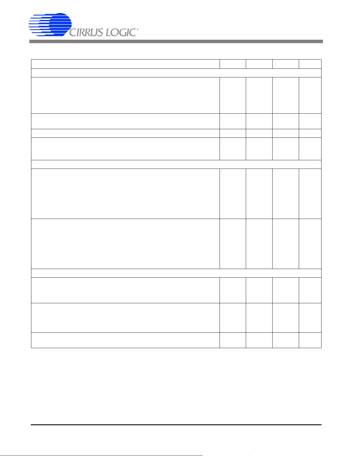
CS5525 CS5526
ANALOG CHARACTERISTICS (Continued)
Parameter Min Typ Max Unit
Analog Input
Common Mode + Signal on AIN+ or AIN- Bipolar/Unipolar Mode
NBV = -1.8 to -2.5 V Range = 25 mV, 55 mV, or 100 mV
Range = 1 V , 2.5 V, or 5 V
NBV = AGND Range = 25 mV, 55 mV, or 100 mV
Range = 1 V , 2.5 V, or 5 V
Common Mode Rejection dc
50, 60 Hz
-0.150
NBV
1.85
0.0
-
-
-
-
-
-
120
120
Input Capacitance - 10 - pF
CVF Current on AIN+ or AIN- (Note 5)
Range = 25 mV, 55 mV, or 100 mV
Range = 1 V , 2.5 V, or 5 V
-
-
100
1.2
System Calibration Specifications
Full-scale Calibration Range Bipolar/Unipolar Mode (Note 9)
25 mV
55 mV
100 mV
1 V
2.5 V
5 V
17.5
38.5
70
0.70
1.75
3.50
-
-
-
-
-
-
Offset Calibration Range Bipolar/Unipolar Mode
25 mV
55 mV
100 mV (Note 10)
1 V
2.5 V
5 V
-
-
-
-
-
-
-
-
-
-
-
-
Power Supplies
DC Power Supply Currents (Normal Mode) I
I
NBV
A+
I
D+
Power Consumption Normal Mode (Note 11)
Low Power Mode
Standby
Sleep
Power Supply Rejection dc Positive Supplies
dc NBV
-
-
-
-
-
-
-
-
-
1.65
15
475
9.4
4.9
1.2
500
95
110
0.950
VA+
2.65
VA+
-
-
300
-
32.5
71.5
105
dB
dB
pA
µA/V
mV
mV
mV
1.30
3.25
VA+
±12.5
±27.5
±50
mV
mV
mV
±0.5
±1.25
±2.50
2.2
30
700
12.7
8.5
-
-
-
-
mA
µA
µA
mW
mW
mW
µW
dB
dB
V
V
V
V
V
V
V
V
V
V
Notes: 9. The minimum Full-scale Calibration Range (FSCR) is limited by the maximum allowed gain register
value (with margin). The maximum FSCR is limited by the ∆Σ modulator’s 1’s density range.
10. The maximum full-scale signal can be limited by saturation of circuitry within the internal signal path.
11. All outputs unloaded. All input CMOS levels.
DS202F5 3
Page 4
CS5525 CS5526
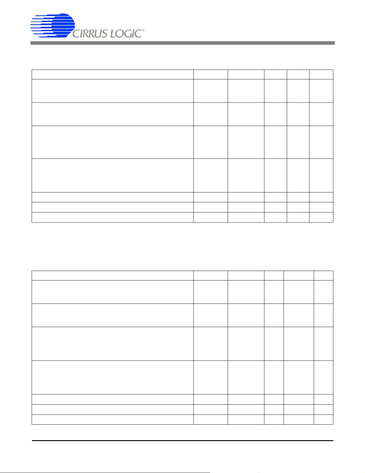
5 V DIGITAL CHARACTERISTICS (T
= 25 °C; VA+, VD+ = 5 V ±5%; GND = 0;
A
See Notes 2 and 12.))
Parameter Symbol Min Typ Max Unit
High-level Input Voltage All Pins Except XIN and SCLK
XIN
SCLK
Low-level Input Voltage All Pins Except XIN and SCLK
XIN
SCLK
High-level Output Voltage
All Pins Except CPD and SDO (Note 13)
CPD, I
SDO, I
= -4.0 mA
out
= -5.0 mA
out
Low-level Output Voltage
All Pins Except CPD and SDO, I
CPD, I
SDO, I
= 1.6 mA
out
= 2 mA
out
= 5.0 mA
out
Input Leakage Current I
3-state Leakage Current I
Digital Output Pin Capacitance C
V
IH
0.6 VD+
3.5
(VD+) - 0.45
V
IL
-
0.0
-
V
OH
(VA+) - 1.0
(VD+) - 1.0
(VD+) - 1.0
V
OL
-
-
-
in
OZ
out
-±1±10µA
--±10µA
-9-pF
-
-
-
-
-
-
-
-
-
-
-
-
-
VD+
-
0.8
1.5
0.6
-
-
-
0.4
0.4
0.4
V
V
V
V
V
V
V
V
V
V
V
V
Notes: 12. All measurements performed under static conditions.
13. I
3.0 V DIGITAL CHARACTERISTICS (T
= -100 µA unless stated otherwise. (VOH = 2.4 V @ I
out
= 25 °C; VA+ = 5 V ±5%; VD+ = 3.0 V ±10%; GND = 0;
A
See Notes 2 and 12.))
Parameter Symbol Min Typ Max Unit
High-level Input Voltage All Pins Except XIN and SCLK
XIN
SCLK
Low-level Input Voltage All Pins Except XIN and SCLK
XIN
SCLK
High-level Output Voltage
All Pins Except CPD and SDO, I
CPD, I
SDO, I
= -400 µA
out
= -4.0 mA
out
= -5.0 mA
out
Low-level Output Voltage
All Pins Except CPD and SDO, I
CPD, I
SDO, I
= 400 µA
out
= 2 mA
out
= 5.0 mA
out
Input Leakage Current I
3-state Leakage Current I
Digital Output Pin Capacitance C
out
V
IH
V
IL
V
OH
V
OL
in
OZ
out
= -40 µA.)
0.6 VD+
0.54 VA+
(VD+) - 0.45
0.0
(VA+) - 0.3
(VD+) - 1.0
(VD+) - 1.0
-
-
-
-
-
-
-
-
-
-
-
-
-
-
-
-
-
-
VD+
-
0.16 VD+
1.5
0.6
-
-
-
0.3
0.4
0.4
V
V
V
V
V
V
V
V
V
V
V
V
-±1±10µA
--±10µA
-9-pF
4 DS202F5
Page 5
DYNAMIC CHARACTERISTICS
Parameter Symbol Ratio Unit
Modulator Sampling Frequency f
Filter Settling Time to 1/2 LSB (Full Scale Step) t
CS5525 CS5526
s
s
XIN/2 Hz
1/f
out
s
RECOMMENDED OPERATING CONDITIONS
(AGND, DGND = 0 V; See Note 14.))
Parameter Symbol Min Typ Max Unit
DC Power Supplies Positive Digital
Positive Analog
Analog Reference V oltage (VREF+) - (VREF-) VRef
VD+
VA+
diff
2.7
4.75
5.0
5.0
5.25
5.25
1.0 2.5 3.0 V
V
V
Negative Bias Voltage NBV -1.8 -2.1 -2.5 V
Notes: 14. All voltages with respect to ground.
ABSOLUTE MAXIMUM RATINGS (AGND, DGND = 0 V; See Note 14.)
Parameter Symbol Min Max Unit
DC Power Supplies (Note 15)
Positive Digital
Positive Analog
Negative Bias Voltage Negative Potential NBV +0.3 -3.0 V
Input Current, Any Pin Except Supplies (Note 16 and 17) I
Output Current I
Power Dissipation (Note 18) PDN - 500 mW
Analog Input Voltage VREF pins
AIN Pins
Digital Input Voltage V
Ambient Operating Temperature T
Storage Temperature T
VD+
VA+
IN
OUT
V
INR
V
INA
IND
A
stg
-0.3
-0.3
+6.0
+6.0
V
V
-±10mA
-±25mA
-0.3
NBV - 0.3
(VA+) + 0.3
(VA+) + 0.3
V
V
-0.3 (VD+) + 0.3 V
-40 85 °C
-65 150 °C
Notes: 15. No pin should go more negative than NBV - 0.3 V.
16. Applies to all pins including continuous overvoltage conditions at the analog input (AIN) pins.
17. Transient current of up to 100 mA will not cause SCR latch-up. Maximum input current for a power
supply pin is ±50 mA.
18. Total power dissipation, including all inpu t currents and output currents.
WARNING: Operation at or beyo nd these limits may result in permanent damage to the device.
Normal operation is not guaranteed at these extremes.
DS202F5 5
Page 6
CS5525 CS5526
SWITCHING CHARACTERISTICS (T
Input Levels: Logic 0 = 0 V, Logic 1 = VD+; C
= 50 pF.))
L
= 25 °C; VA+ = 5 V ±5%; VD+ = 3.0 V ±10% or 5 V ±5%;
A
Parameter Symbol Min Typ Max Unit
Master Clock Frequency (Note 19)
Internal Clock
External Clock
XIN
30
30
32.768
32.768
36
100
kHz
Master Clock Duty Cycle 40 - 60 %
Rise Times (Note 20)
Any Digital Input Except SCLK
SCLK
Any Digital Output
Fall Times (Note 20)
Any Digital Input Except SCLK
SCLK
Any Digital Output
t
t
rise
fall
-
-
-
-
-
-
-
-
50
-
-
50
1.0
100
-
1.0
100
-
µs
µs
ns
µs
µs
ns
Start-up
Oscillator Start-up Time XTAL = 32.768 kHz (Note 21) t
Power-on Reset Period t
ost
por
-500-ms
- 1003 - XIN
cycles
Serial Port Timing
Serial Clock Frequency SCLK 0 - 2 MHz
SCLK Falling to CS
Falling for continuous running SCLK
t
0
100 - - ns
(Note 22)
Serial Clock Pulse Width High
Pulse Width Low
t
1
t
2
250
250
-
-
-
-
ns
ns
SDI Write Timing
CS
Enable to Valid Latch Clock t
Data Set-up Time prior to SCLK rising t
Data Hold Time After SCLK Rising t
SCLK Falling Prior to CS
Disable t
3
4
5
6
50 - - ns
50 - - ns
100 - - ns
100 - - ns
SDO Read Timing
to Data Valid t
CS
SCLK Falling to New Data Bit t
Rising to SDO Hi-Z t
CS
7
8
9
--150ns
--150ns
--150ns
Notes: 19. Device parameters are specified with a 32.768 kHz clock; however, clocks up to 100 kHz can be used
for increased throughput.
20. Specified using 10% and 90% points on wa veform of interest. Output loaded with 50 pF.
21. Oscillator start-up time varies with crystal parameters. This specification does not apply when using an
external clock source.
22. Applicable when SCLK is continuously running.
6 DS202F5
Page 7
CS
CS
SCLK
CS5525 CS5526
t
0
t
t
t
3
1
t
2
Continuous Running SCLK Timing (Not to Scale)
t
3
6
CS
SDO
SCLK
SCLK
t
7
MSB
MSB
MSB-1 LSBSDI
t
4
t
5
t
1
t
2
t
6
SDI Write Timing (Not to Scale)
t
9
MSB-1 LSB
t
8
t
2
t
1
SDO Read Timing (Not to Scale)
DS202F5 7
Page 8
CS5525 CS5526
DETAILED DESCRIPTION
The CS5525 and CS5526 are 16-bit and 20-bit pin
compatible converters which include a chopperstabilized instrumentation amplifier input, and an
on-chip programmable gain amplifier. They are
both optimized for measuring low-level unipolar or
bipolar signals in process control and medical applications.
The CS5525/26 also include a fourth order deltasigma modulator, a calibration microcontroller,
eight digital filters, a 4-bit analog latch, and a serial
port. The digital filters provide any one of eight
different output update rates.
The CS5525/26 include a CPD (Charge Pump
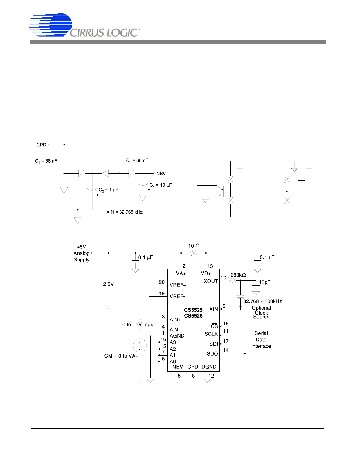
Drive) output (shown in Figure 1). CPD provides a
negative bias voltage to the on-chip instrumentation amplifier when used with a combination of external diodes and capacitors. This enables the
CS5525/26 to measure negative voltages with re-
spect to ground, making the converters ideal for
thermocouple temperature measurements.
Theory of Operation
The CS5525/26 A/D converters are designed to operate from a single +5 V analog supply and provide
several different input ranges. See the Analog
Characteristics section on page 3 for details.
Figure 1 illustrates the CS5525/26 connected to
generate their own negative bias supply using the
on-chip CPD (Charge Pump Drive). This enables
the CS5525/26 to measure ground referenced signals with magnitudes down to NBV (Negative Bias
Voltage, approximately -2.1 V in this example).
Figure 2 illustrates a charge pump circuit when the
converters are powered from a +3.0 V digital supply. Alternatively, the negative bias supply can be
generated from a negative supply voltage or a resistive divider as illustrated in Figure 3.
Figure 1. CS5525/26 Configured to use on-chip charge pump to supply NBV.
8 DS202F5
Page 9
CS5525 CS5526
Figure 4 illustrates the CS5525/26 connected to
measure ground referenced unipolar signals of a
positive polarity using the 1 V, 2.5 V, and 5 V input
voltage ranges on the converter. For the 25 mV, 55
mV, and 100 mV ranges the signal must have a
common mode near +2.5 V (NBV = 0V).
The CS5525/26 are optimized for the measurement
of thermocouple outputs, but they are also well
suited for the measurement of ratiometric bridge
transducer outputs. Figure 5 illustrates the
CS5525/26 connected to measure the output of a
ratiometric differential bridge transducer while operating from a single +5 V supply.
2N5087
or similar
NBV
10µF
+
Figure 2. Charge Pump Drive Circuit for VD+ = 3 V. Figure 3. Alternate NBV Circuits.
-5V
34.8K
30.1K
2.0K
NBV
2.1K
-5V
+
10 µF
Figure 4. CS5525/26 Configured for ground-referenced Unipolar Signals.
DS202F5 9
Page 10

CS5525 CS5526
Figure 5. CS5525/26 Configured for Single Supply Bridge Measurement.
System Initialization
When power to the CS5525/26 is applied, they are
held in a reset condition until their 32.768 kHz oscillators have started and their start-up counter-timer elapses. Due to the high Q of a 32.768 kHz
crystal, the oscillators take 400-600 ms to start. The
converter’s counter-timer counts no more than
1024 oscillator clock cycles to make sure the oscillator is fully stable. During this time-out period the
serial port logic is reset and the RV (Reset Valid)
bit in the configuration register is set. A reset can be
initiated at any time by writing a logic 1 to the RS
(Reset System) bit in the configuration register.
This automatically sets the RV bit until the RS bit
is written to logic 0, and the configuration register
is read. After a reset, the on-chip registers are initialized to the following states and the converters
are ready to perform conversions.
Command Operation
The CS5525/26 include a microcontroller with five
registers used to control the converter. Each register is 24-bits in length except the 8-bit command
register (command, configuration, offset, gain, and
conversion data). After a system initialization or reset, the serial port is initialized to the command
mode and the converter stays in this mode until a
valid 8-bit command is received (the first 8-bits
into the serial port). Table 1 lists all the valid commands. Once a valid 8-bit command (a read or a
write command word) is received and interpreted
by the command register, the serial port enters the
data mode. In data mode the next 24 serial clock
pulses shift data either into or out of the serial port
(72 serial clock pulses are needed if set-up register
is selected). See Table 2 for configuring the
CS5525/26.
configuration register: 000040(H)
offset register: 000000(H)
gain register: 800000(H)
10 DS202F5
Page 11

CS5525 CS5526
Reading/Writing On-Chip Registers
The CS5525/26’s offset, gain, and configuration
registers are read/writable while the conversion
data register is read only.
CC, and PS/R bits must be logic 0 and the CB (MSB)
bit must be a logic 1. The register to be written is selected with the RSB2-RSB0 bits of the command
word. Figure 6 illustrates the serial sequence necessary to write to, or read from the serial port.
To perform a read from a specific register, the R/W
bit of the command word must be a logic 1. The SC,
CC, and PS/R bits must be logic 0 and the CB
(MSB) bit must be a logic 1. The register to be written is selected with the RSB2-RSB0 bits of the
command word.
If the Set-up Registers are chosen with the RSB2RSB0 bits, the registers are read or written in the
following sequence: Offset, Gain and Configuration. This is accomplished by following one 8-bit
command word with three 24-bit data words for a
total of 72 data bits.
To perform a write to a specific register, the R/W
bit of the command word must be a logic 0. The SC,
Command Register
D7(MSB)D6D5D4D3D2D1D0
CB SC CC R/W
RSB2 RSB1 RSB0 PS/R
BIT NAME VALUE FUNCTION
D7 Command Bit, CB 0
D6 Single Conversion, SC 0
D5 Continuous Conversions,
CC
D4 Read/Write
D3-D1 Register Select Bit,
RSB2-RSB0
D0 Power Save/Run
, R/W 0
000
001
010
011
100
101
110
111
, PS/R 0
Table 1. Command Set
1
1
0
1
1
1
Null command (no operation). All command bits, including
CB must be 0.
Logic 1 for executable commands.
Single Conversion not active.
Perform a conversion.
Continuous Conversions not active.
Perform conversions continuously.
Write to selected register.
Read from selected register.
Offset Register
Gain Register
Configuration Register
Conversion Data Register (read only)
Set-up Registers (Offset, Gain, Configuration)
Reserved
Reserved
Reserved
Run
Power Save
DS202F5 11
Page 12

CS5525 CS5526
Confi
guration Register
D23(MSB) D22 D21 D20 D19 D18 D17 D16 D15 D14 D13 D12
A3 A2 A1 A0 NU CFS NU LPM WR2 WR1 WR0 U/B
D11 D10 D9 D8 D7 D6 D5 D4 D3 D2 D1 D0
G2 G1 G0 PD RS RV PF PSS DF CC2 CC1 CC0
BIT NAME VALUE FUNCTION
D23-D20 Latch Outputs, A3-A0 0000 R* Latch Output Pins A3-A0 mimic the D23-D20 Register bits.
D19 Not Used, NU 0 R Must always be logic 0.
D18 Chop Frequency Select,
CFS
D17 Not Used, NU 0 R Must always be logic 0.
D16 Low Power Mode, LPM 0
D15-D13 Word Rate, WR2-0
Note: For
XIN = 32.768kHz
D12 Unipolar/Bipolar
D11-D9 Gain Bits, G2-G0 000
D8 Pump Disable, PD 0
D7 Reset System, RS 0
D6 Reset Valid , RV 0
D5 Port Flag, PF 0
D4 Power Save Select, PSS 0
D3 Done Flag, DF 0
D2-D0 Calibration Control Bits,
CC2-CC0
, U/B 0
0
1
1
000
001
010
011
100
101
110
111
1
001
010
011
100
101
110/111
1
1
1R
1
1
1
000
001
010
011
100
101
110
111
R 256 Hz Amplifier chop frequency
32768 Hz Amplifier chop frequency
R Normal Mode
Reduced Power mode
R 15.0 Sps (2182 XIN cycles)
30.1 Sps (1090 XIN cycles)
60.0 Sps (546 XIN cycles)
123.2 Sps (266 XIN cycles)
168.9 Sps (194 XIN cycles)
202.3 Sps (162 XIN cycles)
3.76 Sps (8722 XIN cycles)
7.51 Sps (4362 XIN cycles)
R Bipolar Measurement mode
Unipolar Measurement mode
R 100 mV (assumes VREF = 2.5V)
55 mV
25 mV
1V
5.0 V
2.5 V
Not Used.
R Charge Pump Enabled
For PD = 1, the CPD pin goes to a Hi-Z output state.
R Normal Operation
Activate a Reset cycle. To return to Normal Operation write bit to zero.
No reset has occurred or bit has been cleared (read only).
Valid Reset has occurred. (Cleared when read.)
R Port Flag mode inactive
Port Flag mode active
R Standby Mode (Oscillator active, allows quick power-up)
Sleep Mode (Oscillator inactive)
R Done Flag bit is cleared (read only).
Calibration or Conversion cycle completed (read only).
R Normal Operation (no calibration)
Offset -- Self-Calibration
Gain -- Self-Calibration
Offset Self-Calibration followed by Gain Self-Calibration
Not used.
Offset -- System Calibration
Gain -- System Calibration
Not Used.
* R indicates the bit value after the part is reset
Table 2. Configuration Register
12 DS202F5
Page 13

CS5525 CS5526
CS
SCLK
SDI
CS
SCLK
SDI
SDO
Command Time
8 SCLKs
Command Time
8 SCLKs
MSB
Write Cycle
MSB
Read Cycle
LSB
Data Time 24 SCLKs
(or 72 S C LKs for Set-up R e gisters)
LSB
Data Tim e 24 S C LK s
(or 72 S C LKs for Set-up Registers)
SCLK
SDI
t *
Command Time
8 SCLKs
SDO
* td = XIN/OWR clock cycles for each conversion except the
first conversion which will take XIN/OWR + 7 clock cycles
d
SDO Continuous Conversion Read (PF bit = 1)
8 SCLKs Clear SDO Flag
MSB
Data Time
24 SCLKs
XIN/OWR
Clock Cycles
LSB
Figure 6. Command and Data Word Timing.
DS202F5 13
Page 14

CS5525 CS5526
Analog Input
Figure 7 illustrates a block diagram of the analog input signal path inside the CS5525/26. The front end
consists of a chopper-stabilized instrumentation amplifier with 20X gain and a programmable gain section. The instrumentation amplifier is powered from
VA+ and from the NBV (Negative Bias Voltage) pin
allowing the CS5525/26 to be operated in either of
two analog input configurations. The NBV pin can
be biased to a negative voltage between -1.8 V and
-2.5 V, or tied to AGND. The choice of the operating
mode for the NBV voltage depends upon the input
signal and its common mode voltage.
For the 25 mV, 55 mV, and 100 mV input ranges, the
input signals to AIN+ and AIN- are amplified by the
20X instrumentation amplifier. For ground referenced signals with magnitudes less then 100 mV, the
NBV pin should be biased with -1.8 V to -2.5 V. If
NBV is tied between -1.8 V and -2.5 V, the (Common Mode + Signal) input on AIN+ and AIN- must
stay between -0.150 V and 0.950 V to ensure proper operation. Alternatively, NBV can be tied to
AGND where the input (Common Mode + Signal)
on AIN+ and AIN- must stay between 1.85 V and
2.65 V to ensure that the amplifier operates properly.
For the 1 V, 2.5 V, and 5 V input ranges, the instrumentation amplifier is bypassed and the input signals are directly connected to the Programmable
Gain block. With NBV tied between -1.8 V and
-2.5 V, the (Common Mode + Signal) input on
AIN+ and AIN- must stay between NBV and VA+.
Alternatively, NBV can be tied to AGND where
the input (Common Mode + Signal) on AIN+ and
AIN- pins can span the entire range between
AGND and VA+.
The CS5525/26 can accommodate full scale ranges
other than 25 mV, 55 mV, 100 mV, 1 V, 2.5 V and
5 V by performing a system calibration within the
limits specified. See the Calibration section for
more details. Another way to change the full scale
range is to increase or to decrease the voltage reference to other than 2.5 V. See the Voltage Refer-
ence section for more details.
Three factors set the operating limits for the input
span. They include: instrumentation amplifier saturation, modulator 1’s density, and a lower reference
voltage. When the 25 mV, 55 mV or 100 mV range
is selected, the input signal (including the common
mode voltage and the amplifier offset voltage)
must not cause the 20X amplifier to saturate in either its input stage or output stage. To prevent saturation the absolute voltages on AIN+ and AINmust stay within the limits specified (refer to the
‘Analog Input’ table on page 3). Additionally, the
differential output voltage of the amplifier must not
exceed 2.8 V. The equation
ABS(VIN + VOS) x 20 = 2.8 V
defines the differential output limit, where
VIN = (AIN+) - (AIN-)
is the differential input voltage and VOS is the absolute maximum offset voltage for the instrumentation amplifier (VOS will not exceed 40 mV). If the
VREF+
AIN+
AIN-
NBV
14 DS202F5
X20
Figure 7. Block Diagram of Analog Signal Path
Programmable
Gain
Differential 4th
order delta-
sigm a modulator
VREF-
Dig ital F ilter
Page 15

CS5525 CS5526
Input Range
± 25 mV
± 55 mV
± 100 mV
± 1.0 V - 2.5V 2.5 ± 1.0 V ± 1.5 V
± 2.5 V - 2.5V 1.0 ± 2.5 V ± 5.0 V
± 5.0 V - 2.5V 0.5 ± 5.0 V 0V, VA+
Note: 1. The converter's actual input range, the delta-sigma's nominal full scale input, and the delta-sigma's
(1)
maximum full scale input all scale directly with the value of the voltage reference. The values in the
table assume a 2.5 V VREF voltage.
Table 3. Relationship between Full Scale Input, Gain Factors, and Internal Analo g Signal Limitations
differential output voltage from the amplifier exceeds 2.8 V, the amplifier may saturate, which will
cause a measurement error.
The input voltage into the modulator must not
cause the modulator to exceed a low of 20 percent
or a high of 80 percent 1's density. The nominal full
scale input span of the modulator (from 30 percent
Max. Differential Output
20X Amplifier
(2)
2.8 V
(2)
2.8 V
(2)
2.8 V
VREF Gain Factor
2.5V 5 ± 0.5 V ± 0.75 V
2.5V 2.272727... ± 1.1 V ± 1.65 V
2.5V 1.25 ± 2.0 V ± 3.0 V
Note: Residual noise appears in the converter’s baseband for
output word rates greater than 60 Sps if CFS is logic 0. By setting CFS to logic 1, the amplifier’s chop frequency chops at
32768 Hz eliminating the residual noise, but increa sing the
current. Note that C=48pF is for input current modeling only.
For physical input capacitance see ‘Input Capacitance’ specification under ‘Analog Characteristics’ on page 3.
25mV, 55mV, and 100mV Ranges
∆-Σ Nominal
Differential Input
(1)
(1)
∆-Σ
Max. Input
to 70 percent 1’s density) is determined by the
VREF voltage divided by the Gain Factor. See Table 3 to determine if the CS5525/26 are being used
properly. For example, in the 55 mV range to determine the nominal input voltage to the modulator,
divide VREF (2.5 V) by the Gain Factor (2.2727).
When a smaller voltage reference is used, the re-
AIN
V ≤ 25mV
os
i = fV C
osn
CF S = 0 , f = 256 H z
CF S = 1 , f = 32.76 8 k H z
C = 48pF
sulting code widths are smaller causing the converter output codes to exhibit more changing codes
for a fixed amount of noise. Table 3 is based upon
a VREF = 2.5 V. For other values of VREF, the values in Table 3 must be scaled accordingly.
Figure’s 8 and 9 illustrate the input models for the
AIN and VREF pins. The dynamic input current for
AIN+
Figure 8. Input models for AIN+ and AIN- pins
1V, 2.5 V, and 5V Ranges
AIN-
i = [(V ) - (V )] fC
n
AIN+ AIN-
f = 32.768 kHz
C = 32pF
each of the pins can be determined from the models
shown and is dependent upon the setting of the CFS
(Chop Frequency Select) bit. The effective input
VREF+
VREF-
C = 16pF
impedance for the AIN+ and AIN- pins remains
i = [(V REF +) - (VR EF -)] fC
constant for the three low level measurement ranges (25 mV, 55 mV, and 100 mV). The input current
is lowest with the CFS bit cleared to logic 0.
Figure 9. Input model for VREF+ and VREF- pins.
n
f = 32.768 kHz
DS202F5 15
Page 16

CS5525 CS5526
Charge Pump Drive
The CPD (Charge Pump Drive) pin of the converters can be used with external components (shown
in Figure 1) to develop an appropriate negative bias
voltage for the NBV pin. When CPD is used to generate the NBV, the NBV voltage is regulated with
an internal regulator loop referenced to VA+.
Therefore, any change on VA+ results in a proportional change on NBV. With VA+ = 5 V, NBV’s
regulation is set proportional to VA+ at approximately -2.1 V.
Figure 3 illustrates a means of supplying NBV voltage from a -5 V supply. For ground based signals
with the instrumentation amplifier engaged (when
in the 25mV, 55mV, or 100mV ranges), the voltage
on the NBV pin should at no time be less negative
than -1.8 V or more negative than -2.5 V. To prevent excessive voltage stress to the chip the NBV
voltage should not be more negative than -3.0 V.
The components in Figure 1 are the preferred components for the CPD filter. However, smaller capacitors can be used with acceptable results. The
10
µF ensures very low ripple on NBV. Intrinsic
safety requirements prohibit the use of electrolytic
capacitors. In this case, two 0.47 µF ceramic capacitors in parallel can be used.
The CPD pin itself is a tri-state output and enters
tri-state whenever the converters are placed into the
Sleep Mode, Standby Mode, or when the charge
pump is disabled (when the Pump Disable bit, bit
D8 in the configuration register, is set). Once in tristate, the digital current can increase if this CPD
output floats near 1/2 digital supply. To ensure the
CPD pin stays near ground and to minimize the
digital current, add a 5MΩ resistor between it and
DGND (see Figure 1). If the resistor is left out, the
digital supply current may increase from 2 µA to 10
µA.
Voltage Reference
The CS5525/26 are specified for operation with a
2.5 V reference voltage between the VREF+ and
VREF- pins of the devices. For a single-ended reference voltage, such as the LT1019-2.5, the reference’s output is connected to the VREF+ pin of the
CS5525/26. The ground reference for the LT1019-
2.5 is connected to the VREF- pin.
The differential voltage between the VREF+ and
VREF- can be any voltage from 1.0 V up to 3.0 V,
however, the VREF- pin can not go below analog
ground.
Calibration
The CS5525/26 offer five different calibration
functions including self calibration and system calibration. However, after the CS5525/26 are reset,
they can perform measurements without being calibrated. In this case, the converters will utilize the
initialized values of the on-chip registers (Gain =
1.0, Offset = 0.0) to calculate output words for the
±100 mV range. Any initial offset and gain errors
in the internal circuitry of the chips will remain.
The gain and offset registers, which are used for
both self and system calibration, are used to set the
zero and full-scale points of the converter’s transfer
i 0=
∑
-24
pro-
-23
). The
N
i–
function. One LSB in the offset register is 2
portion of the input span (bipolar span is 2 times the
unipolar span). The MSB in the offset register determines if the offset to be trimmed is positive or
negative (0 positive, 1 negative). The converters
can typically trim ±50 percent of the input span.
The gain register spans from 0 to (2 - 2
decimal equivalent meaning of the gain register is
Db020b121–b222–… bN2
++++ bi2
==
N–
where the binary numbers have a value of either
zero or one (b
corresponds to the MSB). Refer to
0
Table 4 for details.
16 DS202F5
Page 17

CS5525 CS5526
Offset Register
MSB LSB
-2
-3
-4
-5
Register
Reset (R) 000000 000000
Sign
2
2
2
2
-6
2
-19
2
≈
-20
2
-21
2
-22
2
-23
2
-24
2
One LSB represents 2
-24
proportion of the input span (bipolar span is 2 times unipolar span)
Offset and data word bits align by MSB (bit MSB-4 of offset register changes bit MSB-4 of data)
Gain Register
MSB LSB
0
-1
-2
-3
-4
Register
Reset (R) 100000 000000
The gain register span is from 0 to (2-2
2
2
2
2
2
-23
). After Reset the MSB = 1, all other bits are 0.
-5
2
Table 3.
Table 4. Offset and Gain Registers
The offset and gain calibration steps each take one
conversion cycle to complete. At the end of the calibration step, the calibration control bits will be set
back to logic 0, and the DF (Done Flag) bit will be
set to a logic 1. For the combination self-calibration (CC2-CC0= 011; offset followed by gain), the
calibration will take two conversion cycles to complete and will set the DF bit after the gain calibration is completed. The DF bit will be cleared any
time the data register, the offset register, the gain
register, or the setup register is read. Reading the
configuration register alone will not clear the DF
bit.
-18
2
-19
2
-20
2
-21
2
-22
2
2
≈
of the modulator are connected together and then
routed to the VREF- pin as shown in Figure 11.
For self-calibration of gain, the differential inputs
of the modulator are connected to VREF+ and
S1
OPEN
AIN+
AIN-
S2
CLOSED
+
X20
-
-23
+
-
Self Calibration
Figure 10. Self Calibration of Offset (Low Ranges).
The CS5525/26 offer both self offset and self gain
calibrations. For the self-calibration of offset in the
25 mV, 55 mV, and 100 mv ranges, the converter
internally ties the inputs of the instrumentation amplifier together and routes them to the AIN- pin as
shown in Figure 10. For proper self-calibration of
offset to occur in the 25 mV, 55 mV, and 100 mV
AIN+
AIN-
VREF-
+
X20
-
ranges, the AIN- pin must be at the proper common-mode-voltage (i.e. AIN- = 0V, NBV must be
between -1.8 V to -2.5 V). For self-calibration of
offset in the 1.0 V, 2.5 V, and 5 V ranges, the inputs
DS202F5 17
Figure 11. Self Calibration of Offset (High Ranges).
S1
OPEN
S2
OPEN
S4
CLOSED
S3
CLOSED
+
-
Page 18

Reference
+
-
AIN+
AIN-
VREF+
VREF-
CS5525 CS5526
OPEN
+
X20
OPEN
CLOSED
CLOSED
+
-
External
Connections
+
0V
-
+
CM
-
AIN+
AIN-
+
X20
-
+
-
Figure 12. Self Calibration of Gain (All Ranges).
VREF- as shown in Figure 12. For any input range
other than the 2.5 V range, the modulator gain error
can not be completely calibrated out. This is due to
the lack of an accurate full scale voltage internal to
the chips. The 2.5 V range is an exception because
the external reference voltage is 2.5 V nominal and
is used as the full scale voltage. In addition, when
self-calibration of gain is performed in the 25 mV,
55 mV, and 100 mV input ranges, the instrumentation amplifier’s gain is not calibrated. These two
factors can leave the converters with a gain error of
up to ±20% after self-calibration of gain. Therefore, a system gain is required to get better accuracy, except for the 2.5 V range.
System Calibration
For the system calibration functions, the user must
supply the converters calibration signals which represent ground and full scale. When a system offset
calibration is performed, a ground reference signal
must be applied to the converter. See Figures 13
and 14. As shown in Figures 15 and 16, the user
must input a signal representing the positive full
scale point to perform a system gain calibration. In
either case, the calibration signals must be within
the specified calibration limits for each specific
calibration step (refer to the System Calibration
Specifications).
Figure 13. System Calibration of Offset (Low Ranges).
External
Connections
0V
CM
AIN+
+
-
AIN-
+
-
+
X20
-
+
-
Figure 14. System Calibration of Offset (High Ranges).
External
Connections
+
X20
-
Full Scale
CM
AIN+
+
-
AIN-
+
-
Figure 15. System Calibration of Gain (Low Ranges)
External
Connections
+
X20
-
Full Scale
CM
AIN+
+
-
AIN-
+
-
+
-
+
-
Figure 16. System Calibration of Gain (High Ranges).
18 DS202F5
Page 19

CS5525 CS5526
Assuming a system can provide two known voltages, equations can allow the user to manually compute the calibration register’s values based on two
uncalibrated conversions. The offset and gain calibration registers are used to adjust a typical conversion as follows:
Rc = (Ru + Co>>4) * Cg / 2
23
.
Calibration can be performed using the following
equations:
Co = (Rc0/G - Ru0) << 4
Cg = 2
23
* G
where G = (Rc1 - Rc0)/(Ru1-Ru0).
Note: Uncalibrated conversions imply that the gain and offset
registers are at default {gain register = 0x800000 (Hex) and
offset register = 0x000000 (Hex)}.
The variables are defined below.
V0 = First calibration voltage
V1 = Second calibration voltage (greater than V0)
Ru = Result of any uncalibrated conversion
Ru0 = Result of uncalibrated conversion V0
(20-bit integer or 2’s complement)
Ru1 = Result of uncalibrated conversion of V1
(20-bit integer or 2’s complement)
Rc = Result of any conversion
Rc0 = Desired calibration result of converting V0
(20-bit integer or 2’s complement)
Rc1 = Desired calibration result of converting V1
(20-bit integer or 2’s complement)
Co = Offset calibration register value (24-bit 2’s
complement)
Cg = Gain calibration register value
(24-bit integer)
>> = The shift right operator (e.g. x >>2 is x shift-
ed right 2 bits)
<< = The shift left operator (e.g. x<<2 is x
shifted left 2 bits)
Note: The shift operators are used here to align the decimal
points of words of various lengths. Data to the right of the
decimal point may be used in the calculations shown. For the
CS5525 all conversion results (Ru, Rc...) are 16 bits instead
of 20 bits. To get the equations to work correctly pad the 16
bit results with four zeros (on the right).
Calibration Tips
Calibration steps are performed at the output word
rate selected by the WR2-WR0 bits of the configuration register. Since higher word rates result in
conversion words with more peak-to-peak noise,
calibration should be performed at lower output
word rates. Also, to minimize digital noise near
the devices, the user should wait for each calibration step to be completed before reading or writing
to the serial port.
For maximum accuracy, calibrations should be performed for offset and gain for each gain setting (selected by changing the G2-G0 bits of the
configuration register). And if factory calibration is
performed using the system calibration capabilities
of the CS5525/26, the offset and gain register contents can be read by the system microcontroller and
recorded in EEPROM. These same calibration
words can then be uploaded into the offset and gain
registers of the converters when power is first applied to the system, or when the gain range is
changed.
Two final tips include two ways to determine when
calibration is complete: 1) wait for SDO to fall. It
falls to logic 0 if the PF (Port Flag) bit of the configuration register is set to logic 1; or 2) poll the DF
(Done Flag) bit in the configuration register which
is set at completion of calibration. Whichever
method is used, the calibration control bits (CC2CC0) will return to logic 0 upon completion of any
calibration.
Limitations in Calibration Range
System calibration can be limited by signal headroom in the analog signal path inside the chip as
discussed under the Analog Input section of this
data sheet. System calibration can also be limited
by the intrinsic gain errors of the instrumentation
amplifier and the modulator. For gain calibrations
DS202F5 19
Page 20

CS5525 CS5526
the input signal can be reduced to the point in
which the gain register reaches its upper limit of 2.0
(decimal) [FFFFFF Hex] (this is most likely to occur with an input signal approximately 1/2 the
nominal range). Alternatively, the input signal can
be increased to a point in which the modulator
reaches its one’s density upper limit of 80% (this is
most likely to occur with an input signal approximately 1.5 times the nominal range). Also, for full
scale inputs larger than the nominal full scale value
of the range selected, there is some voltage at
which the various internal circuits may saturate due
to limited amplifier headroom (this is most likely to
occur on the 100 mV range setting when NBV = -
1.8 V).
Analog Output Latch Pins
The A3-A0 pins of the converters mimic the D23D20 bits of the configuration register. A3-A0 can
be used to control multiplexers and other logic
functions outside the converter. The outputs can
sink or source at least 1 mA, but it is recommended
to limit drive currents to less than 20 µA to reduce
self-heating of the chip. These outputs are powered
from VA+, hence, their output voltage for a logic 1
will be limited to the VA+ voltage.
Serial Port Interface
The CS5525/26 serial interface consist of four pins,
SCLK, SDO, SDI, and CS. The CS pin must be
held low (logic 0) before SCLK transitions can be
recognized by the port logic. The SDO output will
be held at high impedance any time CS is a logic 1.
If the CS
three wire interface.
The SCLK input is designed with a Schmitt-trigger
input to allow an optoisolator with slower rise and
fall times to directly drive the pin.
The SDO output is capable of sinking or sourcing
up to 5 mA to directly drive an optoisolator LED.
SDO will have less than a 400 mV loss in the drive
voltage when sinking or sourcing 5 mA.
pin is tied low, the port can function as a
Serial Port Initialization
The serial port is initialized to the command mode
whenever a power-on reset is performed inside the
converter, when the port initialization sequence is
completed, or whenever a command byte, data
word sequence is completed. The port initialization
sequence involves clocking 15 (or more) bytes of
all 1's, followed by one byte with the following bit
contents (11111110). This sequence places the
chips in the command mode where it waits for a
valid command.
Performing Conversions (With PF bit = 0)
Setting the SC (Single Conversion) bit of the command word to a logic 1 with the CB bit = 1, all other
command bits = 0, the CS5525/CS5526 will perform one conversion. At the completion of the conversion the DF (Done Flag) bit of the configuration
register will be set to a logic 1. The user can read
the configuration register to determine if the DF bit
is set. If DF has been set, a command can be issued
to read the conversion data register to obtain the
conversion data word. The DF bit of the configuration register will be cleared to logic 0 when the
data register, the gain register, the offset register, or
the set-up registers are read. Reading only the configuration register will not clear the DF flag bit.
If an SC command is issued to the converters while
they are performing a conversion, the filter will restart a convolution cycle to perform a new conversion.
Performing Conversions (With PF bit = 1)
Setting the PF bit of the configuration register to a
logic 1 enables the SDO output pin to behave as a
flag signal whenever conversions are completed.
This eliminates the need for the user to read the DF
flag bit of the configuration register to determine if
the conversion data word is available.
If the SC (Single Conversion) command is issued
(SC = 1, CB= 1, all other command bits = 0) the
SDO pin will go low at the completion of a conver-
20 DS202F5
Page 21

CS5525 CS5526
sion. The user would then issue 8 SCLKs (with
SDI = logic 0) to clear the SDO flag. Upon the falling edge of the 8th SCLK, the SDO pin will present
the first bit (MSB) of the conversion word. 24
SCLKs (high, then low) are required to read the
conversion word from the port. The user must not
give an explicit command to read the conversion
data register when the PF bit is set to logic 1. The
data conversion word must be read before a new
command can be entered (if the SC command is
used with PF = 1).
If the CC (Continuous Conversion) command is issued (CC = 1, CB =1, all other command bits = 0)
the SDO pin will go low at the completion of a conversion. The user would then issue 8 SCLKs (with
SDI = logic 0) to clear the SDO flag. Upon the falling edge of the 8th SCLK, the SDO pin will present
the first bit (MSB) of the conversion word. 24
SCLKs (high, then low) are required to read the
conversion word from the port. The user must not
give an explicit command to read the conversion
data register when the PF bit is set to logic 1. When
operating in the continuous conversion mode, the
user need not read every conversion. If the user
does nothing after SDO falls, SDO will rise one
XIN clock cycle before the next conversion word is
available and then fall again to signal that another
conversion word is available. If the user begins to
clear the SDO flag and read the conversion data,
this action must be finished before the conversion
cycle which is occurring in the background is complete if the user wants to be able to read the new
conversion data.
To exit the continuous conversion mode, issue any
valid command to the SDI input when the SDO flag
falls. If a CC command is issued to the converter
while it is performing a conversion, the filter will
restart a convolution cycle to perform a new conversion.
Output Word Rate Selection
The WR2-WR0 bits of the configuration register
set the output conversion word rate of the converters as shown in Table 2. The word rates indicated
in the table assume a master clock of 32.768 kHz.
Upon reset the converters are set to operate with an
output word rate of 15.0 Sps.
Clock Generator
The CS5525/26 include a gate which can be connected with an external crystal to provide the master
clock for the chips. They are designed to operate using a low-cost 32.768 kHz “tuning fork” type crystal. The 32.768 kHz crystal should be connected as
shown in Figure 18. Lead lengths should be minimized to reduce stray capacitance.
The converters will operate with an external
(CMOS compatible) clock with frequencies up to
three times the typical crystal frequency of 32.768
kHz. Figure 17 details the converter’s performance
at increased clock rates.
Figure 17. High Speed Clock Performance
The 32.768 kHz crystal is normally specified as a
time-keeping crystal with tight specifications for
both initial frequency and for drift over temperature.
To maintain excellent frequency stability, these
crystals are specified only over limited operating
temperature ranges (i.e. -10 °C to +60 °C). However,
applications with the CS5525/26 don’t generally require such tight tolerances. When 32.768 kHz tuning
fork crystals are used, it is recommended that protection components, an external resistor and capacitor
as shown in Figure 18, be used.
DS202F5 21
Page 22

Figure 18. Tuning Fork Crystal Connection Diagram
Digital Filter
Attenuation (dB)
-100
-110
-120
-130
0
-10
-20
-30
-40
-50
-60
-70
-80
-90
0
123456
CS5525 CS5526
for OWR = 15.0 Hz
f1 = 47.5 Hz
f2 = 65.5 Hz
fS/2 = XIN/4
f2
f1
7
8 9 10 11 12 13 14 15
Sps
The CS5525/26 have eight different linear phase
digital filters which set the output word rates
(OWRs) as stated in Table 2. These rates assume
that XIN is 32.768 kHz. Each of the filters has a
magnitude response similar to that shown in Figure
19. The filters are optimized to settle to full accuracy every conversion and yield better than 80 dB rejection for both 50 and 60 Hz with output word
rates at or below 15.0 Sps.
The converter’s digital filters scale with XIN. For
example with an output word rate of 15 Hz, the filter’s corner frequency is typically 12.7 Hz. If XIN
is increased to 64.536 kHz the OWR doubles and
the filter’s corner frequency moves to 25.4 Hz.
Output Coding
The CS5525/26 output data in binary format when
operating in unipolar mode and in two's complement when operating in bipolar mode.
The output conversion word is 24 bits, or three
bytes long, as shown in Table 5. The MSB is output
Figure 19. Filter Response
(Normalized to Output Word Rate = 1)
first followed by the rest of the data bits in descending order. For the CS5525 the last byte is composed
of bits D7-D4, which are always logic 1; D3-D2,
which are always logic 0; and bits D1-D0 which are
the two flag bits. For the CS5526 the last byte includes data bits D7-D4, D3-D2 which are always
logic 0 and the two flag bits.
The OF (Overrange Flag) bit is set to a logic 1 any
time the input signal is: 1) more positive than positive full scale, 2) more negative than zero (unipolar
mode), 3) more negative than negative full scale
(bipolar mode). It is cleared back to logic 0 whenever a conversion word occurs which is not overranged.
The OD (Oscillation Detect) bit is set to a logic 1 any
time that an oscillatory condition is detected in the
modulator. This does not occur under normal operating
conditions, but may occur whenever the input to the
converters is extremely overranged. If the OD bit is set,
Output Conversion Data CS5525 (16 bits + flags)
D23 D22 D21 D20 D19 D18 D17 D16 D15 D14 D13 D12 D11 D10 D9 D8 D7 D6 D5 D4 D3 D2 D1 D0
MSB1413121110987654321LSB111100ODOF
Output Conversion Data CS5526 (20 bits + flags)
D23 D22 D21 D20 D19 D18 D17 D16 D15 D14 D13 D12 D11 D10 D9 D8 D7 D6 D5 D4 D3 D2 D1 D0
MSB1817161514131211109 8 7 654321LSB00ODOF
Table 5. Data Conversion Word
22 DS202F5
Page 23

CS5525 CS5526
CS5525 16-Bit Output Coding CS5526 20-Bit Output Coding
Unipolar Input
Voltage
>(VFS-1.5 LSB) FFFF >(VFS-1.5 LSB) 7FFF >(VFS-1.5 LSB) FFFFF >(VFS-1.5 LSB) 7FFFF
VFS-1.5 LSB
VFS/2-0.5 LSB
+0.5 LSB
<(+0.5 LSB) 0000 <(-VFS+0.5 LSB) 8000 <(+0.5 LSB) 00000 <(-VFS+0.5 LSB) 80000
Note: VFS in the table equals the voltage between ground and full scale for any of the unipolar gain ranges, or the
voltage between ± full scale for any of the bipolar gain ranges. See text about error flags under overrange
conditions.
the conversion data bits can be completely erroneous.
The OD flag bit will be cleared to logic 0 when the
modula t o r b e c o mes stable. Table 6 illustrates the output coding for the CS5525/26.
Power Consumption
The CS5525/26 accommodate four power consumption modes: normal, low power, standby, and sleep.
The normal mode, the default mode, is entered after a
power-on-reset and typically consumes 9.4 mW. The
low power mode is an alternate mode that reduces the
Offset
Binary
FFFF
-----
FFFE
8000
-----
7FFF
0001
-----
0000
Bipolar Input
Voltage
VFS-1.5 LSB
-0.5 LSB
-VFS+0.5 LSB
Two's
Complement
7FFF
-----
7FFE
0000
-----
FFFF
8001
-----
8000
Table 6. 5525/26 Output Coding
Unipolar Input
Voltage
VFS-1.5 LSB
VFS/2-0.5 LSB
+0.5 LSB
1.2mW. The standby mode leaves the oscillator and
the on-chip bias generator running. This allows the
converters to quickly return to the normal or low
power mode once the PS/R
If D4 in the configuration register and CB and PS/R
in the command word are set to logic 1, the sleep
mode is entered reducing the consumed power to less
than 500 µW. Since the sleep mode disables the oscillator, approximately a 500ms oscillator start-up delay
period is required before returning to the normal or
low power mode.
Offset
Binary
FFFFF
-----
FFFFE
80000
-----
7FFFF
00001
-----
00000
Bipolar Input
Voltage
VFS-1.5 LSB
-0.5 LSB
-VFS+0.5 LSB
Two's
Complement
7FFFF
-----
7FFFE
00000
-----
FFFFF
80001
-----
80000
bit is set back to a logic 1.
consumed power to 4.9 mW. It is entered by setting
bit D16 (the low power mode bit) in the configuration
register to logic 1. Since the converter’s noise performance improves with increased power consumption,
slightly degraded noise or linearity performance
should be expected in the low power mode. The final
two modes are referred to as the power save modes.
They power down most of the analog portion of the
chips and stop filter convolutions. The power save
modes are entered whenever the PS/R
bit and the CB
bit of the command word are set to logic 1. The particular power save mode entered depends on state of
bit D4 (the Power Save Select bit) in the configura-
PCB Layout
The CS5525/26 should be placed entirely over an analog ground plane with both the AGND and DGND
pins of the device connected to the analog plane.
Place the analog-digital plane split immediately adjacent to the digital portion of the chip.
The XIN pin represents a very high impedance when
used with a crystal, so care should be taken in routing
the trace from the crystal to the XIN pin to keep it as
short as possible. Stray capacitance between the CPD
pin and the XIN pin should be minimizedby keeping
the CPD pin trace away from XIN.
tion register. If D4 is logic 0, the converters enters the
standby mode reducing the power consumption to
DS202F5 23
Page 24

PIN DESCRIPTIONS
CS5525 CS5526
ANALOG GROUND AGND VREF+VOLTAGE REFERENCE INPUT
POSITIVE ANALOG POWER VA+ VREF- VOLTAGE REFERENCE INPUT
DIFFERENTIAL ANALOG INPUT AIN+ CS
DIFFERENTIAL ANALOG INPUT AIN- SDI SERIAL DATA INPUT
NEGATIVE BIAS VOLTAGE NBV A3 LOGIC OUTPUT
LOGIC OUTPUT A0 A2 LOGIC OUTPUT
LOGIC OUTPUT A1 SDO SERIAL DATA OUTPUT
CHARGE PUMP DRIVE CPD VD+ POSITIVE DIGITAL POWER
CRYSTAL IN XIN DGND DIGITAL GROUND
CRYSTAL OUT XOUT SCLK SERIAL CLOCK INPUT
1
2
3
4
5
6
7
8
9
10 11
20
19
18
17
16
15
14
13
12
CHIP SELECT
Clock Generator
XIN; XOUT - Crystal In; Crystal Out, Pins 9, 10.
A gate inside the chip is connected to these pins and can be used with a crystal to provide the
master clock for the device. Alternatively, an external (CMOS compatible) clock can be
supplied into the XIN pin to provide the master clock for the device.
Control Pins and Serial Data I/O
CS - Chip Select, Pin 18.
When active low, the port will recognize SCLK. When high the SDO pin will output a high
impedance state. CS should be changed when SCLK = 0.
SDI - Serial Data Input, Pin 17.
SDI is the input pin of the serial input port. Data will be input at a rate determined by SCLK.
SDO - Serial Data Output, Pin 14.
SDO is the serial data output. It will output a high impedance state if CS
SCLK - Serial Clock Input, Pin 11.
A clock signal on this pin determines the input/output rate of the data for the SDI/SDO pins
respectively. This input is a Schmitt trigger to allow for slow rise time signals. The SCLK pin
will recognize clocks only when CS
is low.
A0, A1, A2, A3 - Logic Outputs, Pin 6, 7, 15, 16.
The logic states of A0-A3 mimic the states of the D20-D23 bits of the configuration register.
Logic Output 0 = AGND, and Logic Output 1 = VA+.
= 1.
24 DS202F5
Page 25

Measurement and Reference Inputs
AIN+, AIN- - Differential Analog Input, Pins 3, 4.
Differential input pins into the device.
VREF+, VREF- - Voltage Reference Input, Pins 20, 19.
Fully differential inputs which establish the voltage reference for the on-chip modulator.
NBV - Negative Bias Voltage, Pin 5.
Input pin to supply the negative supply voltage for the 20X gain instrumentation amplifier.
May be tied to AGND if AIN+ and AIN- inputs are centered around +2.5 V; or it may be tied
to a negative supply voltage (-2.1 V typical) to allow the amplifier to handle low level signals
more negative than ground.
CPD - Charge Pump Drive, Pin 8.
Square wave output used to provide energy for the charge pump.
Power Supply Connections
CS5525 CS5526
VA+ - Positive Analog Power, Pin 2.
Positive analog supply voltage. Nominally +5 V.
VD+ - Positive Digital Power, Pin 13.
Positive digital supply voltage. Nominally +3.0 V or +5 V.
AGND - Analog Ground, Pin 1.
Analog Ground.
DGND - Digital Ground, Pin 12.
Digital Ground.
DS202F5 25
Page 26

SPECIFICATION DEFINITIONS
Linearity Error
The deviation of a code from a straight line which connects the two endpoints of the A/D
Converter transfer function. One endpoint is located 1/2 LSB below the first code transition
and the other endpoint is located 1/2 LSB beyond the code transition to all ones. Units in
percent of full-scale.
Differential Nonlinearity
The deviation of a code's width from the ideal width. Units in LSBs.
Full Scale Error
The deviation of the last code transition from the ideal [{(VREF+) - (VREF-)} - 3/2 LSB].
Units are in LSBs.
Unipolar Offset
The deviation of the first code transition from the ideal (1/2 LSB above the voltage on the
AIN- pin.). When in unipolar mode (U/B
CS5525 CS5526
bit = 1). Units are in LSBs.
Bipolar Offset
The deviation of the mid-scale transition(111...111 to 000...000) from the ideal (1/2 LSB below
the voltage on the AIN- pin). When in bipolar mode (U/B
bit = 0). Units are in LSBs.
26 DS202F5
Page 27

20 PIN PLASTIC (PDIP) PACKAGE DRAWING
D
1
TOP VIEW
DIM MIN MAX MIN MAX
A 0.155 0.180 3.94 4.57
A1 0.020 0.040 0.51 1.02
b 0.015 0.022 0.38 0.56
b1 0.050 0.065 1.27 1.65
c 0.008 0.015 0.20 0.38
D 0.960 1.040 24.38 26.42
E 0.240 0.260 6.10 6.60
e 0.095 0.105 2.41 2.67
eA 0.300 0.325 7.62 8.25
L 0.125 0.150 3.18 3.81
∝
E
A1
A
L
SEATING
PLANE
b1
e
BOTTOM VIEW
b
INCHES MILLIMETERS
0° 15° 0° 15°
CS5525 CS5526
∝
eA
SIDE VIEW
c
Notes: 1. Positional tolerance of leads shall be within 0.25 mm (0.010 in.) at maximum material condition, in
relation to seating plane and each other.
2. Dimension eA to center of leads when formed parallel.
3. Dimension E does not include mold flash.
DS202F5 27
Page 28

CS5525 CS5526
20 PIN SSOP PACKAGE DRAWING
N
1
23
TOP VIEW
D
E
e
2
b
SIDE VIEW
A2
A1
A
SEATING
PLANE
L
INCHES MILLIMETERS
1
E1
END VIEW
NOTE
DIM MIN MAX MIN MAX
A -- 0.084 -- 2.13
A1 0.002 0.010 0.05 0.25
A2 0.064 0.074 1.62 1.88
b 0.009 0.015 0.22 0.38 2,3
D 0.272 0.295 6.90 7.50 1
E 0.291 0.323 7.40 8.20
E1 0.197 0.220 5.00 5.60 1
e 0.024 0.027 0.61 0.69
L 0.025 0.040 0.63 1.03
∝
0° 8° 0° 8°
Notes: 1. “D” and “E1” are reference datums and do not included mold flash or protrusions, but do include mold
mismatch and are measured at the parting li ne, mold flash or protrusions shall not exceed 0.20 mm per
side.
2. Dimension “b” does not include dambar protrusion/intrusion. Allowable dambar protrusion shall be
0.13 mm total in excess of “b” dimension at maximum material condition. Dambar intrusion shall not
reduce dimension “b” by more than 0.07 mm at least material condition.
3. These dimensions apply to the fl at section of the lead between 0.10 and 0.25 mm from lead tips.
28 DS202F5
Page 29

ORDERING INFORMATION
CS5525 CS5526
Model Package
CS5525-AS
20-pin SSOP
CS5525-ASZ (Lead Free)
CS5526-BP 20-pin Plastic Dip (0.300”)
CS5526-BS
20-pin SSOP
CS5526-BSZ (Lead Free)
Linearity Error (Max)
±0.003%
±0.0015%
ENVIRONMENTAL, MANUFACTURING, & HANDLING INFORMATION
Model Number Peak Reflow Temp MSL Rating* Max Fl oor Life
CS5525-AS
CS5525-ASZ (Lead Free)
CS5526-BP
CS5526-BS
CS5526-BSZ (Lead Free)
* MSL (Moisture Sensitivity Level) as specified by IPC/JEDEC J-STD-020.
240 °C 2 365 Days
260 °C 3 7 Days
260 °C 1 No Limit
240 °C 2 365 Days
260 °C 3 7 Days
Temperature
-40 to +85 °C
DS202F5 29
Page 30

REVISION HISTORY
Revision Date Changes
F4 JUN 2005 Added Lead-free device ordering information.
F5 AUG 2005 Revised Lead-free device ordering information. Added MSL data.
CS5525 CS5526
Contacting Cirrus Logic Support
For all product questions and inquiries contact a Cirrus Logic Sales Representative.
To find the one nearest to you go to www.cirrus.com
IMPORTANT NOTICE
Cirrus Logic, Inc. and it s subs i dia ri e s (“Ci r ru s”) be li eve tha t t he in for mat i o n cont ai n ed in t hi s document i s acc ur at e and re l i abl e . Ho wev er , th e in fo rmation is subject
to change without noti ce and is provi ded “AS I S” with out warran ty of any kind ( express or implied ). Cust omers are a dvised to obtain the latest version of relevant
information to verify, before placing orders, tha t inform atio n bei ng relied on is curr ent and com plete. Al l prod ucts are sold s ubject to the ter ms and co nditio ns of sale
supplied at the time of order acknowledgment, including those pertaining to warranty, indemnification, and limitation of liability. No responsibility is assumed by Cirrus
for the use of this information, including use of this information as the basis for manufacture or sale of any items, or for infringement of patents or other rights of third
parties. This document is the property of Ci rrus and by furnishing this information, Cirrus grants no license, express or implied under any patents, mask work rights,
copyrights, trademarks, trade secrets or other intellectual property rights. Cirrus owns the copyrights associated with the information contained herein and gives consent for copies to be made of the information only for use within your organization with respect to Cirrus integrated circuits or other products of Cirrus. This consent
does not extend to other copying such as copying for ge neral distribution, advertising or promotional purposes, or for creating any work for re sa l e.
CERTAIN APPLICATIONS USING SEMICONDUCTOR PRODUCTS MAY INVOLVE POTENTIAL RISKS OF DEATH, PERSONAL INJURY, OR SEVERE PROPERTY OR ENVIRONMENTAL DAMAGE (“CRITICAL APPLICATIONS”). CIRRUS PRODUCTS ARE NOT DESIGNED, AUTHORIZED OR WARRANTED FOR USE
IN AIRCRAFT SYSTEMS, MILITARY APPLICATIONS, PRODUCTS SURGICALLY IMPLANTED INTO THE BODY, AUTOMOTIVE SAFETY OR SECURITY DEVICES, LIFE SUPPORT PRODUCTS OR OTHER CRITICAL APPLICATIONS. INCLUSION OF CIRRUS PRODUCTS IN SUCH APPLICATIONS IS UND ERSTOOD
TO BE FULLY AT THE CUSTOMER'S RISK AND CIRRUS DISCLAIMS AND MAKES NO WARRANTY, EXPRESS, STATUTORY OR IMPLIED, INCLUDING THE
IMPLIED WARRANTIES OF MERCHANTABILITY AND FITNESS FOR PARTICULAR PURPOSE, WITH REGARD TO AN Y CI RR US PRODUCT THAT IS USED
IN SUCH A MANNER. IF THE CUSTOMER OR CUSTOMER'S CUSTOMER USES OR PERMITS THE USE OF CIRRUS PRODUCTS IN CRITICAL APPLICATIONS, CUSTOMER AGREES, BY SUCH USE, TO FULLY INDEMNIFY CIRRUS, ITS OFFICERS, DIRECTORS, EMPLOYEES, DISTRIBUTORS AND OTHER
AGENTS FROM ANY AND ALL LIABILITY, INCLUDING ATTORNEYS' FEES AND COSTS, THAT MAY RESULT FROM OR ARISE IN CONNECTION WITH
THESE USES.
Cirrus Logic, Cirrus, and the Cirrus Logic logo designs are trademarks of Cirrus Logic, Inc. All other brand and product names in this document may be trademarks
or service marks of their respective owners.
SPI is a trademark of Motorola, Inc.
Microwire is a trademark of National Semiconductor Corporation.
30 DS202F5
 Loading...