CS5516
CS5520
16-Bit/20-Bit Bridge Transducer A/D Converter
Features
l On-chip Instrume nta t ion Amplifier
l On-chip Programmable Gain Amplifier
l On-Chip 4-Bit D/A For Offset Removal
l Dynamic Excitation Options
l Linearity Error: ±0.0015% FS
- 20-Bit No Missing Codes
l CMRR at 50/60 Hz > 200 dB
l System Calibration Capability with calibration
read/write option
l 3, 4 or 5 wire Serial Communications Port
l Low Power Consumption: 40 mW
- 10 µW Standby Mode for Portable applications
Description
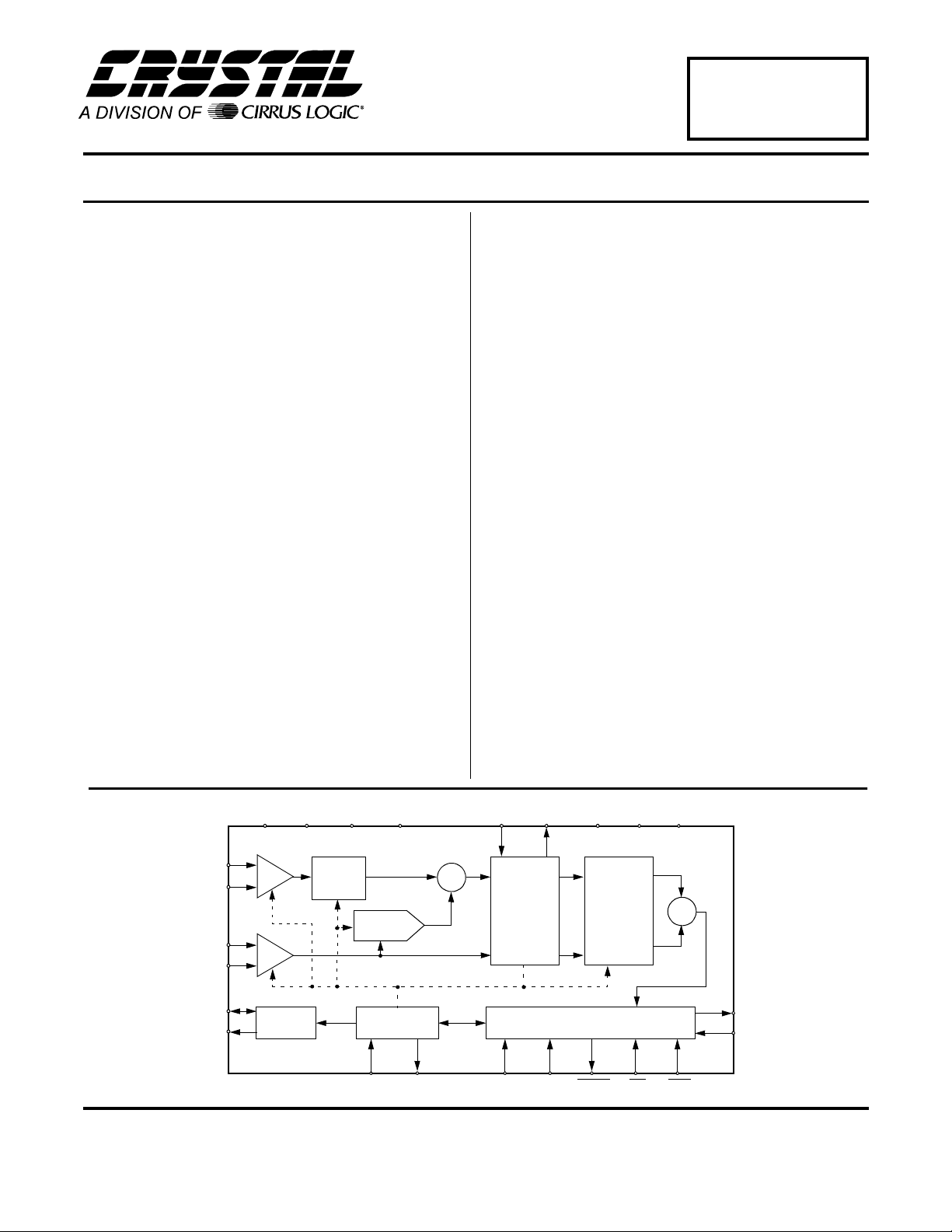
The CS5516 and CS5520 are complete solutions for digitizing low le vel signals from strain gauge s, load cells,
and pressure transducers. Any family of mV output
transducers, includi ng those requiring bridge excitat ion,
can be interfaced directly to the CS5516 or CS5520. The
devices offer an on-chi p software p rogramm able instrumentation amplifier block, choice of DC or AC bridge
excitation, and software selectable reference and signal
demodulation.
The CS5516 uses delta-sigma modulation to achieve
16-bit resolution at outpu t word rates up to 60 Hz. The
CS5520 achieves 20 -bit resolution at word rates u p to
60 Hz.
The CS5516 and CS5520 sample at a rate set by the
user in the form of eith er an external CMOS clock or a
crystal. On-chi p digital filtering provides rejec tion of all
frequencies above 12 Hz for a 4.096 MHz clock.
The CS5516 and CS5520 includ e system calibrat ion to
null offset and gain errors in the input channel. The digital values assoc iate d wi th the sys tem calibration can b e
written to, or read from, the calibration RAM locations at
any time via the serial commun ications port. The 4-bit
DC offset D/A converter, in conjunction with digital correction, is initially used to zero the input offset value.
I
9$9$$*1'$*1'
;
;
%ULGJH
6\QF
*DLQ
%ORFN
$,1
$,1
95()
95()
%;
%;
Cirrus Logic, Inc.
Crystal Semiconductor Products Division
P.O. Box 17847, Austin, Texas 78760
(512) 445 7222 FAX: (512) 445 7581
http://www.crystal.com
ELW'$
&RQYHUWHU
&DOLEUDWLRQ
;,1;287
ORDERING INFORMATION
See page 29.
0'590'599'9''*1'
,1 287
Σ
&KDQQHO
'HOWD6LJPD
0RGXODWRU
,1 287
602'(6&/.'5'<&6567
Copyright Cirrus Logic, Inc. 1997
(All Rights Reserved)
&KDQQHO
),5
)LOWHU
6HULDO,QWHUIDFH
÷
62'
6,'
MAR ‘95
DS74F1
1
CS5516
ANALOG CHARACTERISTICS (T
VREF= 2.5V (externa l differen tial volt age across VREF+ an d VREF-); f
AC Excitation 300 Hz; Gain = 25; Bipolar Mode; R
A
= T
source
MIN
to T
; VA+, VD+, MDRV+ = 5V; VA-, VD- = -5V;
MAX
= 4.9152 MHz ;
CLK
= 300Ω with a 4.7nF to AGND at AIN (see Note 1);
unless otherwise specified.)
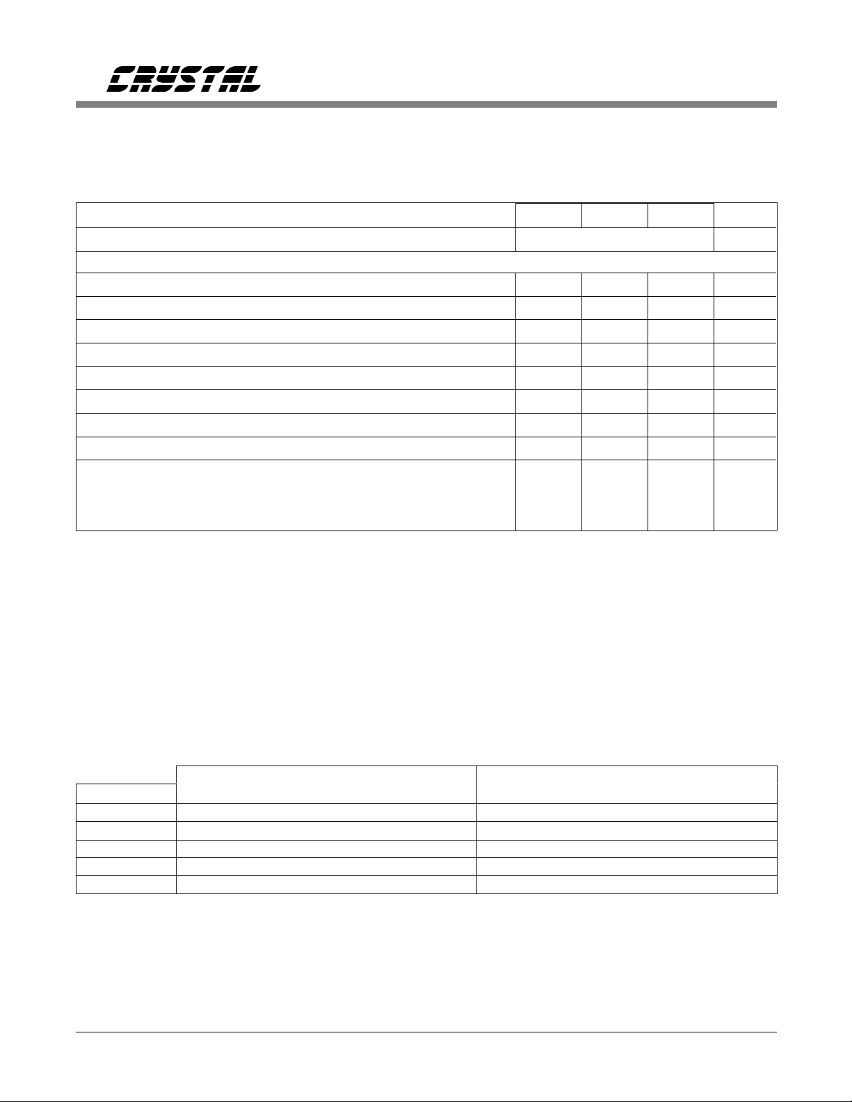
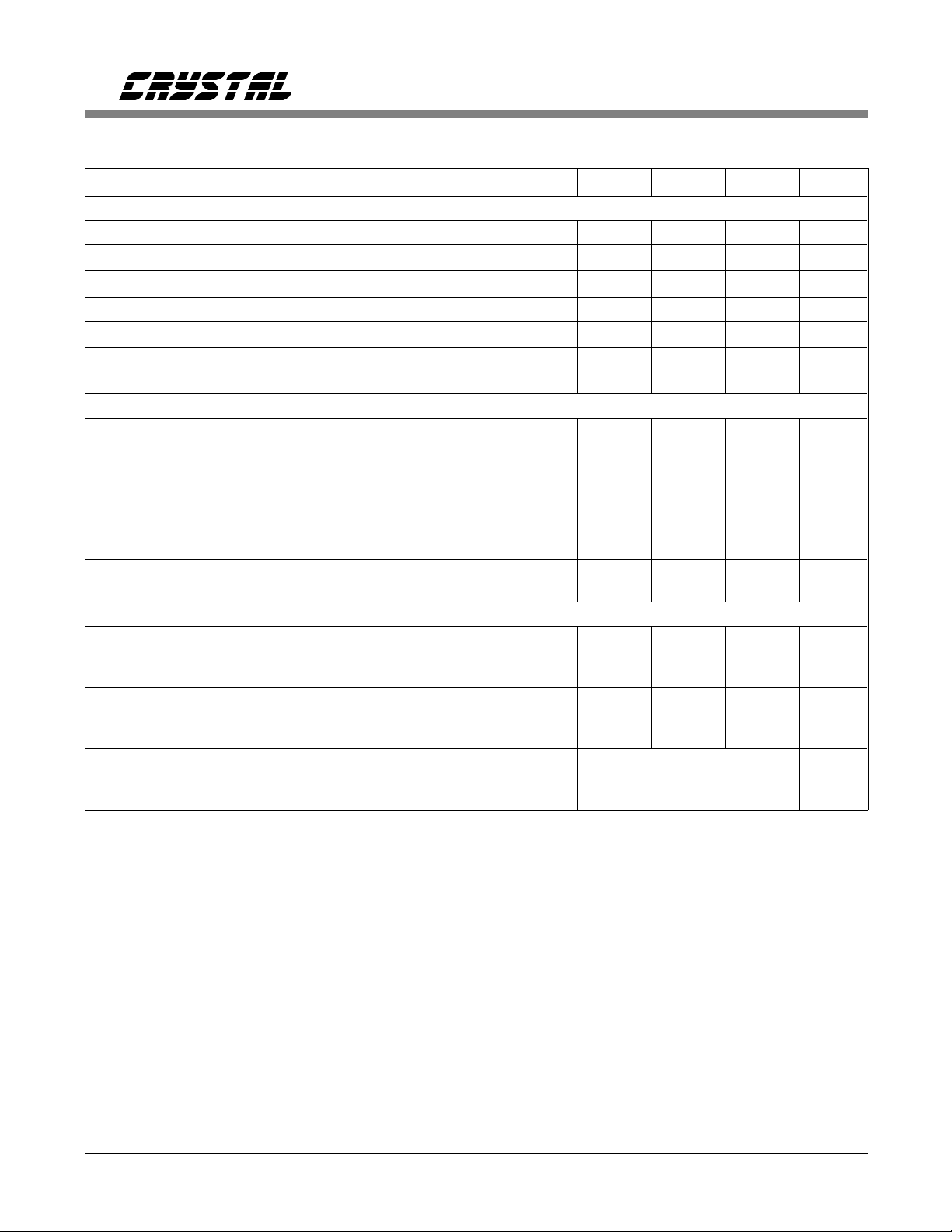
Parameter* Min Typ Max Units
Specified Temperature Range -40 to +85
°
C
Accuracy
Linearity Error - 0.0015 0.003
Differential Nonlinearity Unipolar Gain Error (Note 2) Bipolar Gain Error (Note 2) Unipolar/Bipolar Gain Drift Unipolar Offset (Note 2) Bipolar Offset (Note 2) Offset Drift Noise (Referred to Input) Gain = 25 (25 x 1)
Gain = 50 (25 x 2)
Gain = 100 (25 x 4)
Gain = 200 (25 x 8)
-
-
-
-
±
0.25
±
±
±
±
±
±
0.005
250
200
150
150
±
0.5
8
8
1
1
1
±
31
±
31
-
±
2
±
2
-
-
-
-
-
±
%FS
LSB
16
ppm
ppm
ppm/°C
LSB
16
LSB
16
µV/°
C
nVrms
nVrms
nVrms
nVrms
Notes: 1. The AIN and VREF pins present a very high input resistance at dc and a minor dynamic load which
scales to the master clock fr equency. Both source r esistance and shunt capac itance are therefore
critical in determining the source impedance requirements of the CS5516 and CS5520 at these pins.
2. Applies after system calibration at the temperature of interest.
Unipolar Mode Bipolar Mode
µ
V
LSB’s % FS ppm FS LSB’s % FS ppm FS
0.4 0.26 0.0004 4 0.13 0.0002 2
0.76 0.50 0.0008 8 0.26 0.0004 4
1.52 1.00 0.0015 15 0.50 0.0008 8
3.04 2.00 0.0030 30 1.00 0.0015 15
6.08 4.00 0.0061 61 2.00 0.0030 30
VREF = 2.5V PGA gain = 1
CS5516; 16-Bit Unit Conversion Factors
* Refer to the Specification Definitions immediately following the Pin Description Section.
Specifications are subject to change without notice.
2 DS74F1
ANALOG CHARACTERISTICS (continued)
Parameter* Min Typ Max Units
CS5520
Specified Temperature Range -40 to +85
°
C
Accuracy
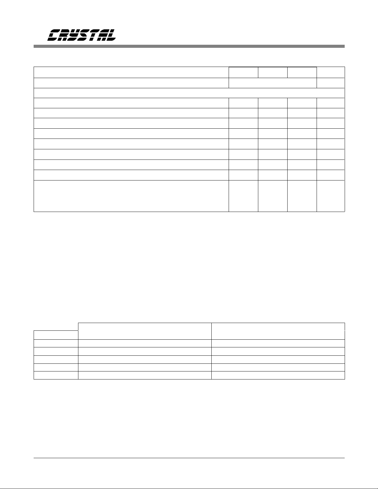
Linearity Error - 0.0007 0.0015
Differential Nonlinearity (No Missing Codes) 20 - - Bits
Unipolar Gain Error (Note 2) Bipolar Gain Error (Note 2) Unipolar/Bipolar Gain Drift Unipolar Offset (Note 2) Bipolar Offset (Note 2) Offset Drift Noise (Referred to Input) Gain = 25 (25 x 1)
Gain = 50 (25 x 2)
Gain = 100 (25 x 4)
Gain = 200 (25 x 8)
-
-
-
-
±
±
±
±
±
±
0.005
250
200
150
150
4
4
1
4
4
±
24
±
24
-
±
8
±
8
-
-
-
-
-
±
%FS
ppm
ppm
ppm/°C
LSB
LSB
µV/°
nVrms
nVrms
nVrms
nVrms
20
20
C
Unipolar Mode Bipolar Mode
µ
V
0.025 0.26 0.0000238 0.25 0.13 0.0000119 0.125
0.047 0.50 0.0000477 0.50 0.26 0.0000238 0.25
0.095 1.00 0.0000954 1.0 0.50 0.0000477 0.50
0.190 2.00 0.0001907 2.0 1.00 0.0000954 1.0
0.380 4.00 0.0003814 4.0 2.00 0.0001907 2.0
* Refer to the Specification Definitions immediately following the Pin Description Section.
DS74F1 3
LSB’s % FS ppm FS LSB’s % FS ppm FS
VREF = 2.5V PGA gain = 1
CS5520; 20-Bit Unit Conversion Factors
Specifications are subject to change without notice.
ANALOG CHARACTERISTICS (continued)
Parameter Min Typ Max Units
CS5516, CS5520
Specified Temperature Range -40 to +85
°
C
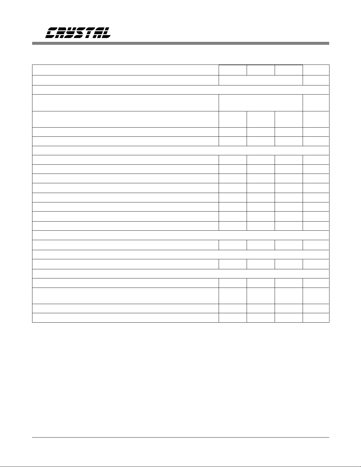
Analog Input
Analog Input Range Unipolar
Bipolar
Common Mode Rejection dc
50, 60 Hz
Input Capacitance - 5 - pF
Input Bias Current (Note 1) - 100 - pA
12.5, 25, 50, 100
±
12.5, ±25, ±50, ±100
-
-
165
200
mV
mV
-
-
dB
dB
Instrumentation Amplifier
Gain - 25 Bandwidth - 200 - kHz
Unity Gain Bandwidth - 5 - MHz
Output Slew Rate - 1.5 -
Noise @ 10 Hz BW - 100 - nV rms
Power Supply Rejection @ 50/60 Hz (Note 3) - 120 - dB
Common Mode Range (Note 4) -
Chopping Frequency - XIN/128 - Hz
±
3
-V
V/µsec
Programmable Gain Amplifier
Gain Tracking (Note 5) -
±
1
-%
4-Bit Offset Trim DAC
Accuracy -
±
5
-%
Voltage Reference Input
Range (Note 6) 2.0 2.5 3.8 V
Common Mode Rejection: dc
50, 60 Hz
Input Capacitance - 15 - pF
Input Bias Current (Note 1) - 10 - nA
Notes: 3. This includes the on-chip digital filtering.
4. The maximum magnitude of the differential input voltage, Vdiff(in) is determined by the following:
Vdiff(in) < 300 mV - |Vcm/12.5 | and should never exceed 300mV .
Vcm is the common mode voltage which is applied to the ins trumentation amplifier inputs.
The above equation should be used to calculate the allowable common mode voltage for a given
differential voltage applied to the firs t gain stage inputs. This limit ensures
that the instrumentation amplifier does not saturate.
5. Gain tracking accuracy can be significantly improved by uploading a calibrated gain word to the
gain register for each PGA gain s election.
6. The common mode voltage on the Voltage Reference Input, plus the reference range,
[(VREF+) - (VREF-)]/2, must not exceed ±3 volts.
-
-
60
200
-
-
dB
4 DS74F1
CS5516, CS5520
ANALOG CHARACTERISTICS (continued)
Parameter Min Typ Max Units
Modulator Differential Voltage Reference
Nominal Output Voltage - 3.75 - V
Initial Output Voltage Tolerance -
Temperature Coefficient - 100 Line Regulation (4.75V < VA < 5.25V) - 0.5 - mV/V
Output Voltage Noise 0.1 to 15 Hz - 10 Output Current Drive: Source Current
Sink Current
-
-
±
100
-
-
Power Supplies
DC Power Supply Currents I
Power Dissipation: (Note 7)
Normal Operation
Standby Mode
Power Supply Rejection: dc Positive Supplies
dc Negative Supplies
I
A+
I
A-
D+
I
D-
-
-
-
-
-
-
-
-
2.7
-2.7
1.5
-0.6
37.5
10
100
95
System Calibration Specifications
Positive Full Scale Calibration Range (Note 8)
Unipolar Mode
Bipolar Mode
Maximum Ratiometric Offset Calibration Range (Note 8)
Unipolar Mode
Bipolar Mode
Differential Input Voltage Range (Notes 4, 8, 9, 10)
Unipolar Mode
Bipolar
Notes: 7. All outputs unloaded. All inputs CMOS levels.
8. T=VREF/(Gx25), where T is the full s cale span, where VREF i s the differential voltage ac ross
VREF+ and VREF- in volts, and G is the gain setting of the second gain block. G can be set
to 1, 2, 4, 8. This sets the overall gain to 25, 50, 100, 200. The gai n can then be fine tuned by
using the calibration of the full s cale point.
9. When calibrated.
10. V
is the offset corrected by the offset c alibration routine. V
offset
0.8T
0.8T
-2T
-2T
Voffset + (1.2T)
Voffset ± (1.2T)
offset
-
-
-
-
may be as large as 2T.
-mV
ppm/°C
µ
V
20
20
3.5
-3.5
2.2
-0.8
-
-
-
-
1.2T
1.2T
+2T
+2T
µ
µ
mA
mA
mA
mA
mW
µ
W
dB
dB
V
V
V
V
V
V
p-p
A
A
DS74F1 5
DYNAMIC CHARACTERISTICS
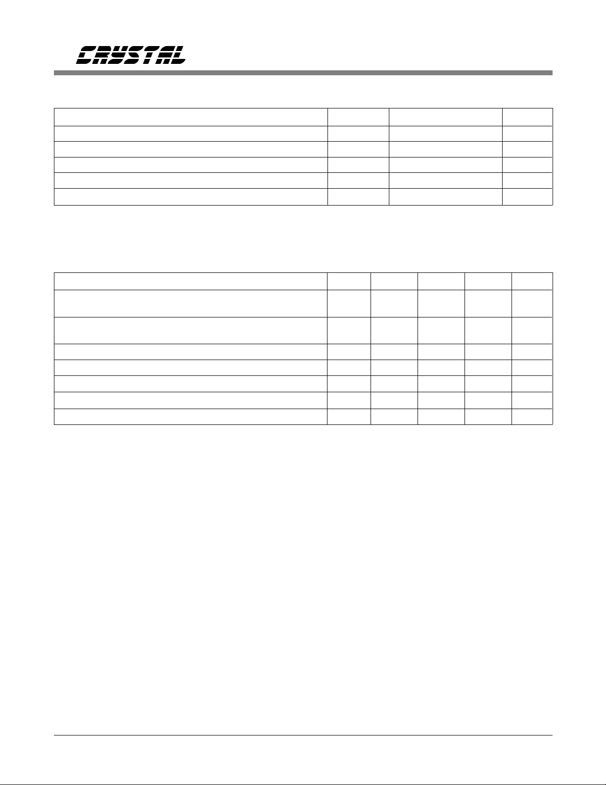
Parameter Symbol Ratio Units
CS5516, CS5520
AIN and VREF Input Sampling Frequency f
Modulator Sampling Frequency f
Output Update Rate f
Filter Corner Frequency f
Settling Time to ±0.0007% (FS Step)
DIGITAL CHARACTERISTICS (T
= T
A
MIN
to T
MAX
is
s
out
-3dB
t
s
; VA+, VD+ = 5V ± 5%; VA-, VD- = -5V ± 5%;
DGND = 0) All measurements below are per formed under static conditions .
Parameter Symbol Min Typ Max Units
High-Level Input Voltage: XIN
All Pins Except XIN
Low-Level Input Voltage XIN
All Pins Except XIN
High-Level Output Voltage (Note 11) V
Low-Level Output Voltage l
= 1.6mA V
out
Input Leakage Current l
3-State Leakage Current l
Digital Output Pin Capacitance C
Notes: 11. I
= -100 µA. This guarantees the ability to drive one TTL load. (VOH = 2.4V @ I
out
V
V
V
V
IH
IH
IL
IL
(VD+)-1.0 - - V
OH
OL
in
OZ
out
f
/128 Hz
clk
f
/256 Hz
clk
f
/81,920 Hz
clk
f
/341,334 Hz
clk
4.5
2.0
-
-
6/f
out
-
-
-
-
-
-
0.5
0.8
s
V
V
V
V
--0.4V
-110
--
±
10
µ
A
µ
A
-9-pF
= -40 µA).
out
6 DS74F1
CS5516, CS5520
RECOMMENDED OPERATING CONDITIONS (AGND, DGND = 0V, see Note 12.)
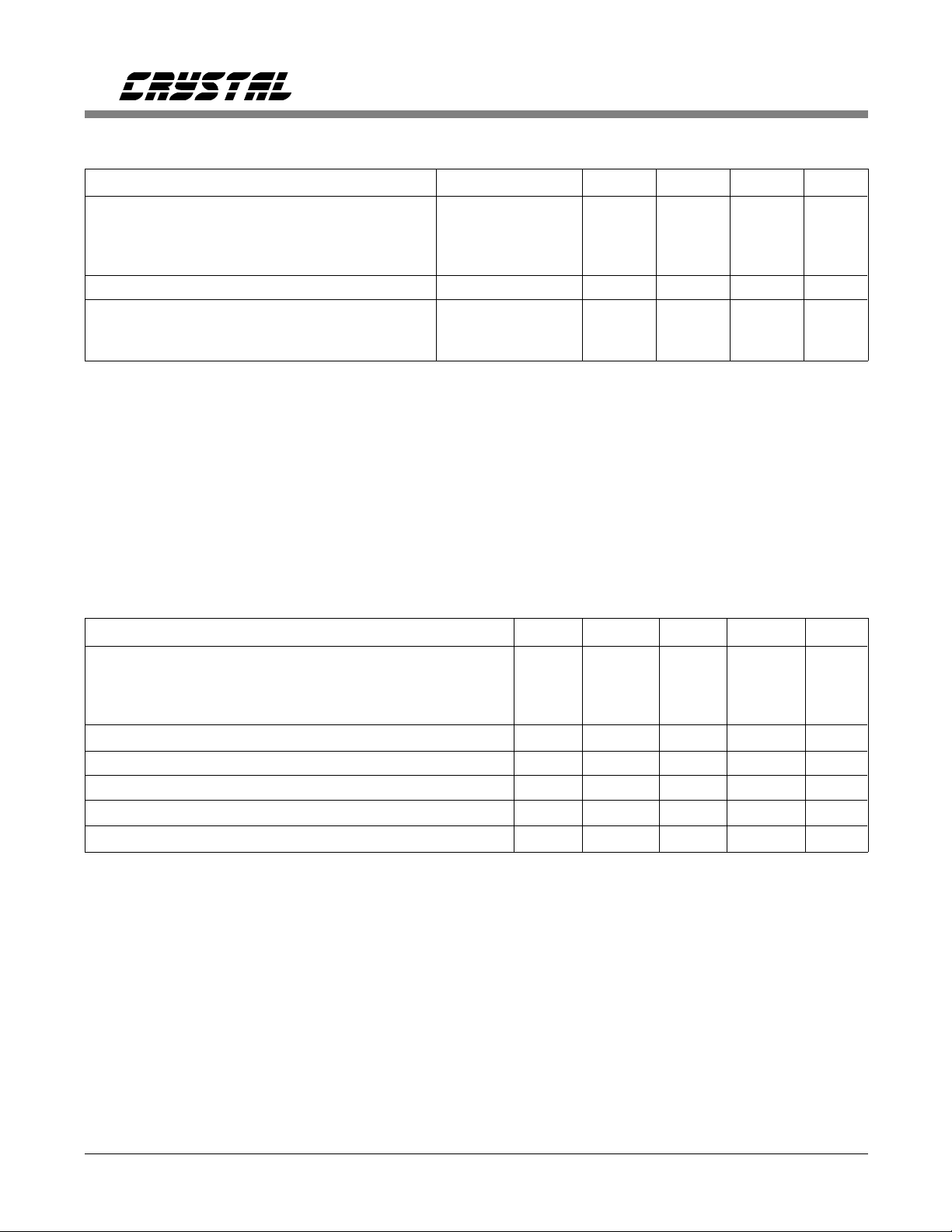
Parameter Symbol Min Typ Max Units
DC Power Supplies: Positive Digital
Negative Digital
Positive Analog
Negative Analog
Differential Analog Reference Voltage (VREF+) - (VREF-) 2.0 2.5 3.8 V
Analog Input Voltage: (Note 13)
Unipolar
Bipolar
Notes: 12. All voltages with respect to ground.
13. The CS5516 and CS5520 can accept input voltages up to +T in unipolar mode and -T to +T in bipolar
mode where T=VREF/(Gx25). G is the gain setting at the second gain block . When the inputs exceed
these values, the CS5516 and CS5520 will output positive full scale for any input abov e T, and
negative full scale for inputs below AGND in unipolar and -T in bipolar mode. This applies when the
analog input does not exceed ±2T overrange.
VD+
VD-
VA+
VA-
VAIN
VAIN
4.5
-4.5
4.5
-4.5
0
-T
5.0
-5.0
5.0
-5.0
-
-
5.5
-5.5
5.5
-5.5
+T
+T
V
V
V
V
V
V
ABSOLUTE MAXIMUM RATINGS* (AGND, DGND = 0V, all voltages with respect to ground.)
Parameter Symbol Min Typ Max Units
DC Power Supplies: Positive Digital (Note 14)
Negative Digital
Positive Analog
Negative Analog
Input Current, Any Pin Except Supplies (Notes 15, 16) l
Analog Input Voltage AIN and VREF pins V
Digital Input Voltage V
Ambient Operating Temperature T
Storage Temperature T
Notes: 14. No pin should go more positive than ( VA+)+0.3V. VD+ must always be less than (VA+)+0.3 V,and
can never exceed 6.0V.
15. Applies to all pins inc luding continuous overvoltage condi tions at the analog input pi ns.
16. Transient currents of up to 100mA will not cause SCR latch-up. Max imum input current for a power
supply pin is ± 50 mA.
* WARNING: Operation beyond these limits may r esult in permanent damage to the device.
Normal operation is not guaranteed at these extremes.
VD+
VD-
VA+
VA-
in
INA
IND
A
stg
-0.3
-0.3
-0.3
+0.3
--
(VA-)-0.3 - (VA+)+0.3 V
-0.3 - (VD+)+0.3 V
-55 - 125
-65 - 150
-
-
-
-
(VA+)+0.3
-5.5
5.5
-5.5
±
10
mA
°
°
V
V
V
V
C
C
DS74F1 7
CS
CS5516, CS5520
SID
SCLK
DRDY
CS
SOD
SCLK
MSB
t
7
t
3
MSB-1
t
4
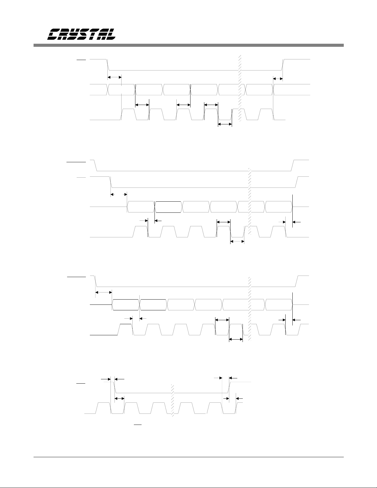
SID Write Timing (Not to Scale)
MSB MSB-1
t
6
t
5
t
1
t
2
LSB
t
8
t
1
t
2
t
9
DRDY
SOD
SCLK
CS
SCLK
SOD Read Timing (Not to Scale)
t
10
MSB MSB-1
t
8
SOD Read Timing with CS = 0 (Not to Scale)
t
12
t
13
CS with Continuous SCLK (Not to Scale)
t
1
LSB
t
9
t
2
t
14
t
15
8 DS74F1
CS5516, CS5520
SWITCHING CHARACTERISTICS (T
VA-, VD- = -5V±5%; Input Levels: Logic 0 = 0V, Logic 1 = VD+; C
A
= T
MIN
to T
VA+, VD+ = 5V ± 5%;
MAX;
= 50 pF)
L
Parameter Symbol Min Typ Max Units
Master Clock Frequency: Internal Oscillator / External Clock XIN 1.0 4.096 5.0 MHz
Master Clock Duty Cycle 40 - 60 %
Rise Times Any Digital Input (Note 18)
Any Digital Output
Fall Times Any Digital Input (Note 18)
Any Digital Output
t
t
rise
fall
-
-
-
-
50
50
-
-
1.0
-
1.0
-
µ
ns
µ
ns
Startup
Power-on Reset Period t
Oscillator Start-up Time X TAL = 4.9152 MHz(Note 19) t
RST Pulse Width t
por
ost
res
- 100 - ms
-60-ms
1/XIN - - ns
Serial Port Timing
Serial Clock Frequency SCLK - - 2.4 MHz
Serial Clock Pulse Width High
Pulse Width Low
t
1
t
2
200
200
-
-
-
-
ns
ns
SID Write Timing
CS Enable to Valid Latch Clock t
Data Set-up Time prior to SCLK rising t
Data Hold Time After SCLK Rising t
SCLK Falling Prior to CS Disable t
3
4
5
6
150 - - ns
50 - - ns
50 - - ns
50 - - ns
SOD Read Timing
CS to Data Valid t
SCLK Falling to New Data Bit t
SCLK Falling to SOD Hi-Z t
DRDY Falling to Valid Data (CS = 0) t
CS Rising to SOD Hi-Z t
CS Disable Hold Time t
CS Enable Set-up Time t
CS Enable Hold Time t
CS Disable Set-up Time t
7
8
9
10
11
12
13
14
15
- - 150 ns
- - 170 ns
- - 200 ns
- - 150 ns
- - 150 ns
50 - - ns
150 - - ns
50 - - ns
150 - - ns
Notes: 18. Specified using 10% and 90% points on waveform of interest. Output loaded wi th 50 pF.
19. Oscillator start-up time var ies with crystal par ameters. This specification does not apply when us ing
an external clock source.
s
s
DS74F1 9
GENERAL DESCRIPTION
CS5516, CS5520
The CS5516 and CS5520 are monolithic CMOS
A/D converters which include an instrumentation
amplifier input, an on-chip programmable gain
amplifier, and a DAC for offset trimming.
While the devices are optimized for ratiometric
measurement of Wheatstone bridge applications,
they can be used for general purpose low-level
signal measurement.
Each of the devices includes a two-channel differential delta-sigma modulator (the signal
measurement input and the reference input are
digitized independently before a digital output
word is computed), a calibration microcontroller,
a two-channel digital filter, a programmable instrumentation amplifier block, a 4-bit DAC for
+5V
Analog
Supply
Bridge
Excitation
Supply
-
Unused logic inputs
must be connected
to DGND or VD+
-5V
Analog
Supply
0.1 µF1 µF1
1 µF
Excitation Supply
Synch. Signals
+
0.1 µF
1 µF 1 µF
coarse offset trimming, circuitry for generation
and demodulation of AC (actually switched DC)
bridge excitation, and a serial port. The CS5516
outputs 16-bit words; the CS5520 outputs 20-bit
words.
The CS5516/20 devices can measure either
unipolar or bipolar signals. Self-calibration is
utilized to maximize performance of the measurement system. To better understand the
capabilities of the CS5516/20, it is helpful to examine some of the error sources in bridge
measurement systems.
10
Ω
µ
F
Optional
Clock
Source
Serial
Data
Interface
Control
Logic
0.1 µF
2
1
12
11
9
10
6
7
5
8
320
10
VD+
SMODE
DGND
VD-
Ω
VA+
MDRVMDRV+
BX1
BX2
VREF+
VREF-
AIN+
AINAGND1
AGND2
VA-
CS5516
CS5520
XOUT
XIN
SCLK
SOD
SID
DRDY
RST
CS
214
0.1 µF
23
22
16
18
17
24
15
13
14
19
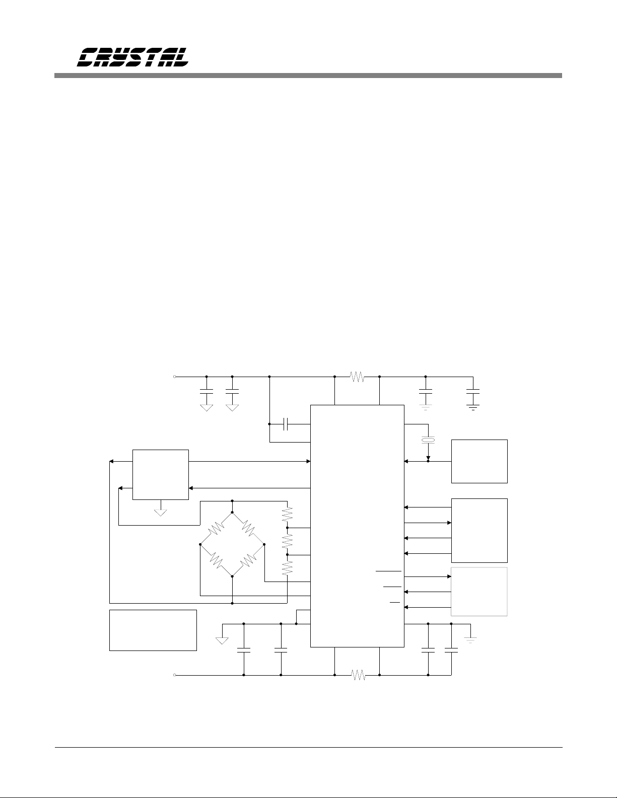
Figure 1. System Connection Diagram: AC Excitation Mode Using External Excitation
10 DS74F1
THEORY OF OPERATION
CS5516, CS5520
The front page of this data sheet illustrates the
block diagram of the CS5516 and CS5520 A/D
converter. The device includes an instrumentation amplifier with a fixed gain of 25. This
chopper-stabilized instrumentation amplifier is
followed by a programmable gain stage with
gain settings of 1, 2, 4, and 8. The sensitivity of
the input is a function of the programmable gain
setting and of the reference voltage connected
between the VREF+ and VREF- pins of the device. The full scale of the converter is VREF/( G
x 25) in unipolar, or ±VREF/(G x 25) in bipolar,
where VREF is the reference voltage between
the VREF+ and VREF- pins, G is the gain setting of the programmable gain amplifier, and 25
is the gain of the instrumentation amplifier.
+5V
Analog
Supply
-
Unused logic inputs
must be connected
to DGND or VD+
-5V
Analog
Supply
0.1 µF1 µF1
1 µF
+
0.1 µF
1 µF 1 µF
After the programmable gain block, the output
of a 4-bit DAC is combined with the input signal. The DAC can be used to add or subtract
offset from the analog input signal. Offsets as
large as ±200 % of full scale can be trimmed
from the input signal.
The CS5516 and CS5520 are optimized to perform ratiometric measurement of bridge-type
transducers. The devices support dc bridge excitation or two modes of ac (switched dc) bridge
excitation. In the switched-dc modes of operation the converter fully demodulates both the
reference voltage and the analog input signal
from the bridge.
10
Ω
µ
F
Optional
Clock
Source
Serial
Data
Interface
Control
Logic
2
1
9
10
6
7
5
8
320
10
VD+
SMODE
DGND
VD-
Ω
VA+
MDRVMDRV+
CS5516
CS5520
VREF+
VREF-
AIN+
AINAGND1
AGND2
VA-
XOUT
XIN
SCLK
SOD
SID
DRDY
RST
CS
214
0.1 µF
23
22
16
18
17
24
15
13
14
19
0.1 µF
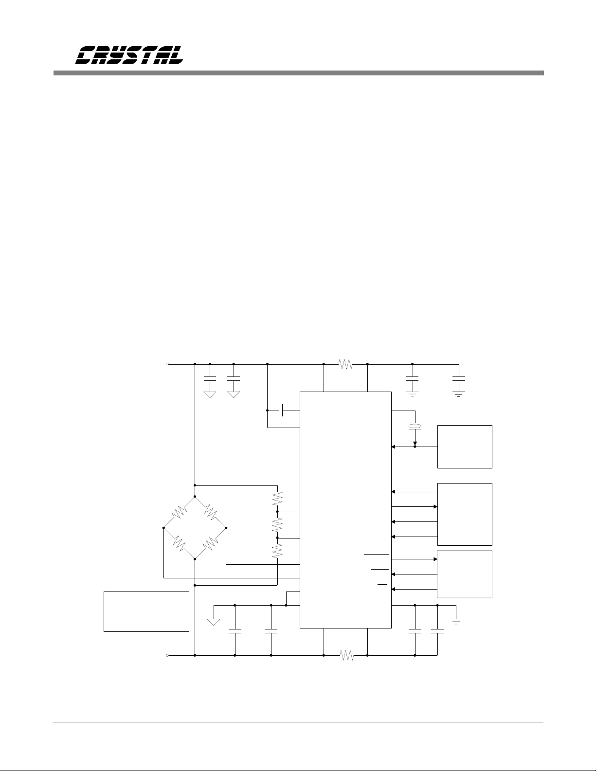
Figure 2. System Connection Diagram: DC Excitation Mode (EXC bit = 0), F1 = F0 = 0.
DS74F1 11
Command Register
D7 D6 D5 D4 D3 D2 D1 D0
1 RSB2 RSB1 RSB0 R/
BIT NAME VALUE FUNCTION
D7 D7 1 Must always be logic 1
RSB2-0 Register Select Bit
000
001
010
011
100
101
110
111
R/W R ead/Write 0
D2
D1
D0
D2
D1
D0
1
0
0
0
Selects Re gister to be Read o r Writte n per R/
CONVERSION DATA (read only )
CONFIGURATION
GAIN
DAC
RATIOMETRIC OFFSET
NON-RATIOMETRIC OFFSET - AIN
NON-RATIOMETRIC OFFSET - VREF
NOT USED
Write to the registe r selected by th e RSB2-0 bi ts
Read from the regi ster selec ted by the RS B2-0 bits
Not Used
Not Used
Not Used
W0 0 0
CS5516, CS5520
W bit
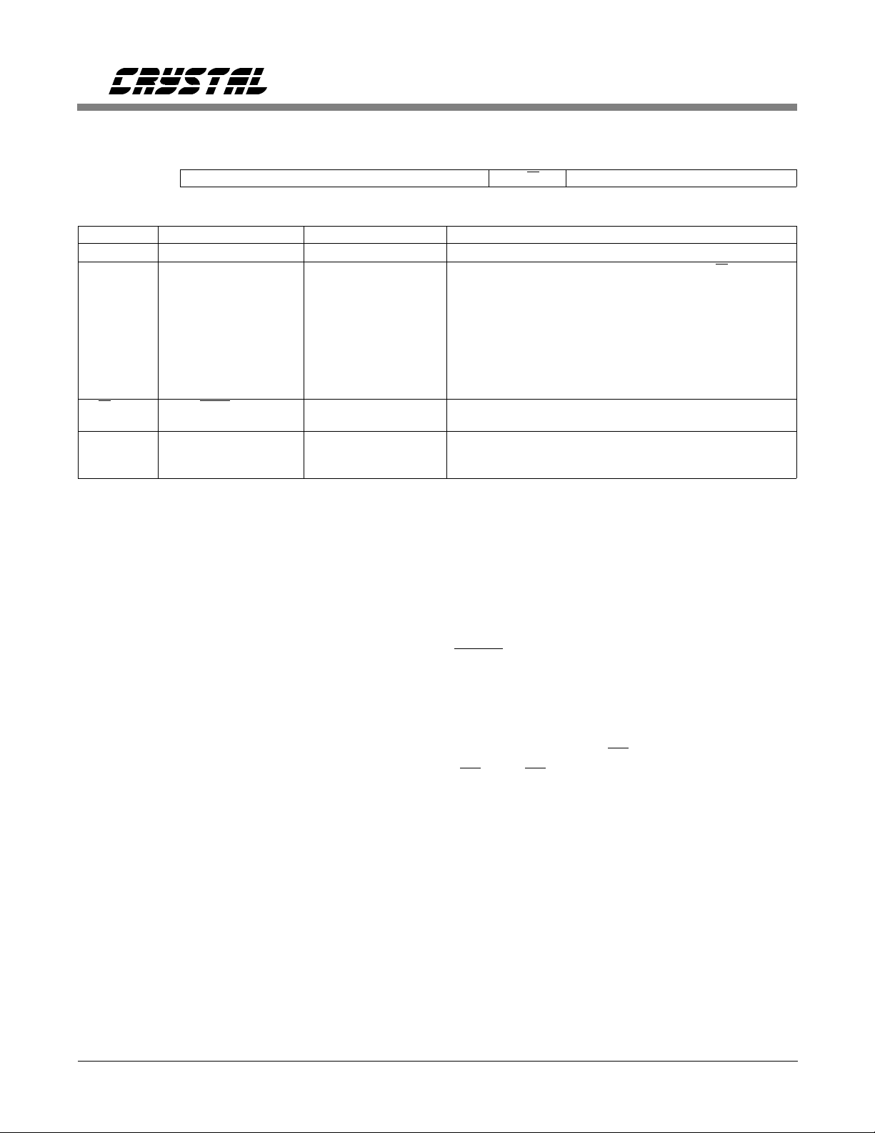
Table 1. CS5516 and CS5520 Commands
The CS5516/20 includes a microcontroller which
manages operation of the chip. Included in the
microcontroller are eight different registers associated with the operation of the device. An 8-bit
command register is used to interpret instructions received via the serial port. When power
is applied, and the device has been re set, the serial port is initialized into the command mode.
In this mode it is waiting to receive an 8-bit
command via its serial port. The first 8 bits into
the serial port are placed into the command register. Table 1 lists all the valid command words
for reading from or writing to internal registers
of the converter. Once a valid 8-bit command
word has been received and decoded, the serial
port goes into data mode. In data mode the next
24 serial clock pulses shift data either into or out
of the serial port. When writing data to the port,
the data may immediately follow the command
word. When reading data from the port, the user
must pause after clocking in the 8-bit command
word to allow the microcontroller time to decode
the command word, access the appropriate regis-
ter to be read, and present its 24-bit word to the
port. The microcontroller will signal when the
24-bit read data is available by causing the
DRDY pin to go low.
The user must write or read the full 24-bit word
except in the case of reading conversion data. In
read data conversion mode, the user may read
less than 24 bits if CS is then made inactive
(CS = 1). CS going inactive releases user control
over the port and allows new data updates to the
port.
The user can instruct the on-chip microcontroller
to perform certain operations via the configuration register. Whenever a new word is written
to the 24-bit configuration register, the microcontroller then decodes the word and executes
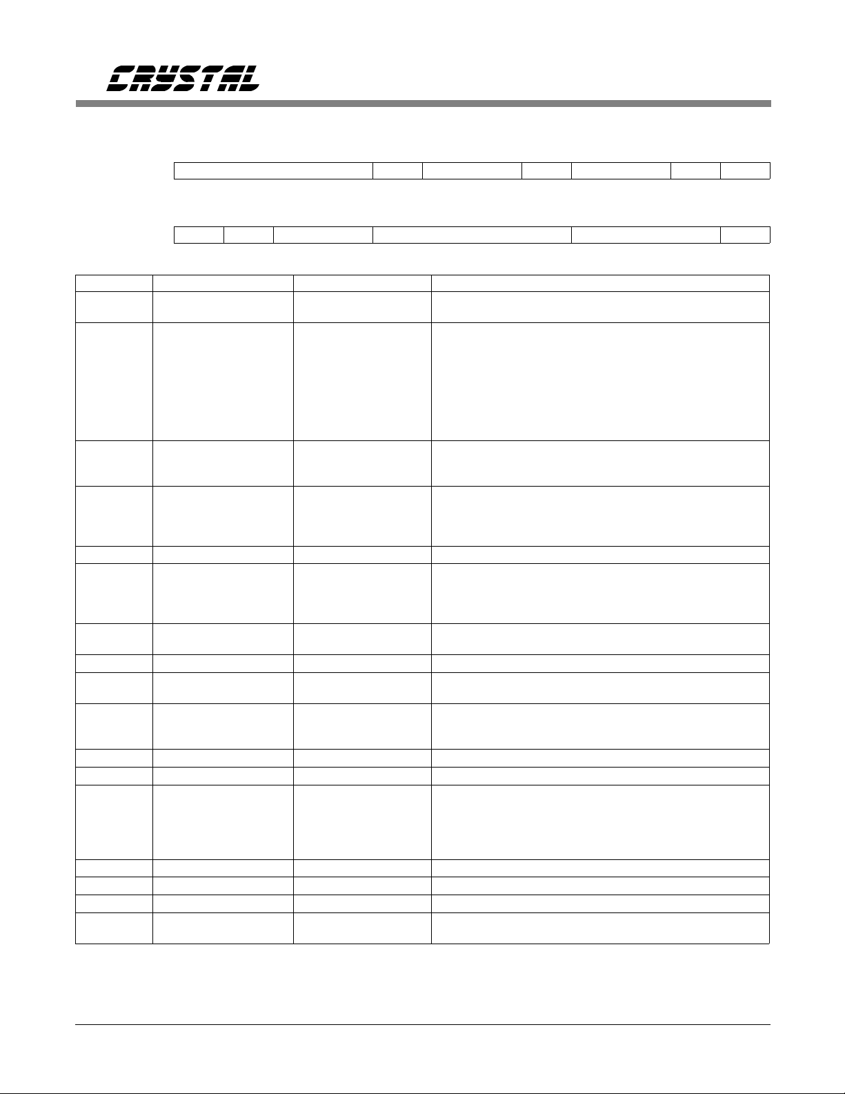
the configuration register instructions. Table 2
illustrates the bits of the configuration register.
The bits in the configuration register will be discussed in various sections of this data sheet.
12 DS74F1
Configuration Register
D23 D22 D21 D20 D19 D18 D17 D16 D15 D14 D13 D12
Register
Reset (R)
Register
Reset (R)
DAC3 DAC2 DAC1 DAC0 EXC F1 F0 D16 G1 G0 U/B D12
000000000000
D11 D10 D9 D8 D7 D6 D5 D4 D3 D2 D1 D0
A/S EC D9 D8 CC3 CC2 CC1 CC0 D3 D2 D1 RF
000000000000
CS5516, CS5520
BIT NAME VALUE FUNCTION
DAC3 DAC Sign Bit 0
1
DAC2-0 DAC Bits 000
001
010
011
100
101
110
111
EXC E xcitatio n: Internal
External
F1-F0 Select Frequenc y 00
D16 D16 0
G1-G0 Select PGA Gain 00
U/B Select Unipolar/B ipo-
lar Mode
D12 D12 0
A/S Awake/ Sleep 0
EC Execute Cali bration 0
D9 D9 0
D8 D8 0
CC3-CC0 Calibration Control Bits 0000
D3 D3 0
D2 D2 0
D1 D2 0
RF Reset Filter 0
0
1
01
10
11
10
01
11
0
1
1
1
1000
0100
0010
0001
1
1
R
Add Offset
Subtract Offset This bit is read only
R
25% Offset
50% Offset
75% Offset
100% Offset These bits are read only
125% Offset
150% Offset
175% Offset
R
R
R
R
R
R
R
R
R
R
R
R
R
R
R
BX1 and BX2 outp uts are de termi ned by bits F1 and F0
BX1 is an input which determines the phase of the
demodulation clock and the BX2 output
Excitation on BX1 & BX2 is dc. BX1=0 V, BX2=+5 V
Excitation Frequency on BX1 & BX2 is XIN/8192 Hz
Excitation Frequency on BX1 & BX2 is XIN/16384 Hz
Excitation Frequency on BX1 & BX2 is XIN/4096 Hz
Must always be logic 0
Gain = 1 (X25)
Gain = 2 (X25)
Gain = 4 (X25)
Gain = 8 (X25)
Bipolar Measureme nt Mode
Unipolar Measurement Mode
Must always be logic 0
Awake Mode
Sleep Mode
Calibration not active
Perform calibratio n select ed by CC 3-CC0 bi ts. EC bi t
must be written back to "0" after calibration is completed
Must always be logic 0
Must always be logic 0
No calibration to be performed
Calibrate non-ratiometric offset, VREF
Calibrate non-ratiometric offset, AIN
Calibrate ratiometric offset, AIN
Calibrate gain, AIN
Must always be logic 0
Must always be logic 0
Must always be logic 0
Normal operation
Reset Filter
2
2
Notes:1.Reset State
2.A write to these bits does not change the register bit values. These bits are just a mirror of the DAC register contents.
Table 2. Configuration Register
DS74F1 13
 Loading...