

Page 1
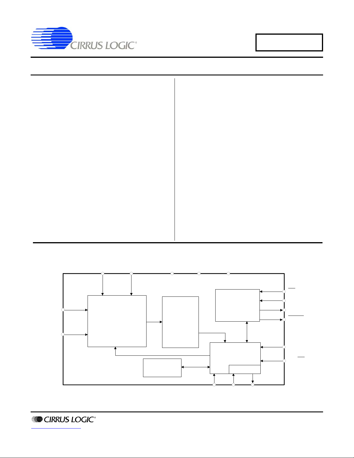
Single-supply, 16-bit A/D Converter
Differential
4th order
delta-sigma
modulator
VD+
13
VA+VREF+9VREF-
10
AIN-
8
AIN+
7
Calibration
SRAM
Serial
Interface
Logic
Digital
Filter
XIN4XOUT
5
CONV
2
Calibration µC
OSC
CAL
3
6
BP/UP
CS
1
DRDY
16
SDATA
15
SCLK
14
11
GND
12
CS5509
Features
Delta-sigma A/D Converter
- 16-bit, No Missing Codes
- Linearity Error: ±0.0015%FS
Differential Input
- Pin-selectable Unipolar/Bipolar Ranges
- Common Mode Rejection
105 dB @ dc
120 dB @ 50, 60 Hz
Either 5V or 3.3V Digital Interface
On-chip Self-calibration Circuitry
Output Update Rates up to 200/second
Ultra Low Power: 1.7 mW
I
Description
The CS5509 is a single-supply, 16-bit, serial-output
CMOS A/D converter. The CS5509 uses charge-balanced (delta-sigma) techniques to provide low-cost,
high-resolution measurements at output word rates up to
200 samples per second.
The on-chip digital filter offers superior line rejection at
50Hz and 60Hz when the device is operated from a
32.768 kHz clock (output word rate = 20 Sps).
The CS5509 has on-chip self-calibration circuitry which
can be initiated at any time or temperature to ensure
minimum offset and full-scale errors.
Low power, high resolution, and small package size
make the CS5509 an ideal solution for loop-powered
transmitters, panel meters, weigh scales, and battery
powered instruments.
ORDERING INFORMATION
CS5509-ASZ -40 °C to +85 °C 16-pin SOIC Lead Free
http://www.cirrus.com
Copyright Cirrus Logic, Inc. 2009
(All Rights Reserved)
SEP ‘09
DS125F3
1
Page 2
CS5509
ANALOG CHARACTERISTICS (T
VREF- = 0V; f
= 32.768 kHz; Bipolar Mode; R
CLK
= 25 °C; VA+ = 5V ±5%; VD+ = 3.3V ±5%; VREF+ = 2.5V,
A
= 40 Ω with a 10 nF to GND at AIN; AIN- = 2.5V; unless oth-
source
erwise specified.) (Notes 1 and 2)
Parameter* Min Typ Max Unit
Accuracy
Linearity Error f
= 32.768 kHz
CLK
f
= 165 kHz
CLK
f
= 247.5 kHz
CLK
f
= 330 kHz
CLK
-
-
-
-
0.0015
0.0015
0.0015
0.005
0.003
0.003
0.003
0.0125
± %FS
± %FS
± %FS
± %FS
Differential Nonlinearity - ±0.25 ±0.5 LSB
Full-scale Error (Note 3) - ±0.25 ±2 LSB
Full-scale Drift (Note 4) - ±0.5 - LSB
Unipolar Offset (Note 3) - ±0.5 ±2 LSB
Unipolar Offset Drift (Note 4) - ±0.5 - LSB
Bipolar Offset (Note 3) - ±0.25 ±1 LSB
Bipolar Offset Drift (Note 4) - ±0.25 - LSB
Noise (Referred to Output) - 0.16 -
LSB
Analog Input
Analog Input Range Unipolar
Bipolar (Notes 5 and 6)
Common Mode Rejection dc
f
= 32.768 kHz 50, 60 Hz (Note 2)
CLK
-
-
-
120
0 to +2.5
±2.5
105
-
-
-
-
-
V
V
dB
dB
Input Capacitance - 15 - pF
DC Bias Current (Note 1) - 5 - nA
Power Supplies
DC Power Supply Currents I
Total
I
Analog
I
Digital
-
-
-
350
300
60
450
-
-
µA
µA
µA
Power Dissipation (Note 7) - 1.7 2.25 mW
Power Supply Rejection - 80 - dB
rms
Notes: 1. Both source resistance and shunt capacitance are critical in determining the CS5509's source
impedance requirements. Refer to the text section Analog Input Impedance Considerations.
2. Specifications guaranteed by design, characterization and/or test.
3. Applies after calibration at the temperature of interest.
4. Total drift over the specified temperature range since calibration at power-up at 25 °C.
5. The input is differential. Therefore, GND ≤ Signal + Common Mode Voltage ≤ VA+.
6. The CS5509 can accept input voltages up to the VA+ analog supply. In unipolar mode the CS5509 will
output all 1's if the dc input magnitude ((AIN+) - (AIN-)) exceeds ((VREF+) - (VREF-)) and will output all
0's if the input becomes more negative than 0 Volts. In bipolar mode the CS5509 will output all 1's if the
dc input magnitude ((AIN+) - (AIN-)) exceeds ((VREF+) - (VREF-)) and will output all 0's if the input
becomes more negative in magnitude than -((VREF+) - (VREF-)).
7. All outputs unloaded. All inputs CMOS levels.
* Refer to the Specification Definitions immediately following the Pin Description Section.
2 DS125F3
Page 3
DYNAMIC CHARACTERISTICS
Parameter Symbol Ratio Unit
Modulator Sampling Frequency
Output Update Rate (CONV = 1)
Filter Corner Frequency
Settling Time to 1/2 LSB (FS Step)
f
out
f
-3dB
CS5509
f
f
clk
f
clk
/2
clk
/1622
/1928
1/f
out
Hz
Hz
Hz
s
f
s
t
s
5V DIGITAL CHARACTERISTICS (T
= 25 °C; VA+, VD+ = 5V ±5%; GND = 0) (Notes 2 and 8)
A
Parameter Symbol Min Typ Max Unit
High-level Input Voltage XIN
All Pins Except XIN
V
IH
Low-level Input Voltage XIN
All Pins Except XIN
High-level Output Voltage (Note 9)
Low-level Output Voiltage I
= 1.6 mA V
out
Input Leakage Current
3-State Leakage Current
Digital Output Pin Capacitance
V
IL
V
OH
OL
I
in
I
OZ
C
out
Notes: 8. All measurements are performed under static conditions.
9. I
3.3V DIGITAL CHARACTERISTICS (T
= -100 µA. This guarantees the ability to drive one TTL load. (VOH = 2.4 V at I
out
= 25 °C; VA+ = 5V ±5%; VD+ = 3.3V ±5%; GND = 0)
A
(Notes 2 and 8)
Parameter Symbol Min Typ Max Unit
High-level Input Voltage XIN
All Pins Except XIN
V
IH
Low-level Input Voltage XIN
All Pins Except XIN
High-level Output Voltage (Note 9)
Low-level Output Voltage I
= 1.6 mA V
out
Input Leakage Current
3-state Leakage Current
Digital Output Pin Capacitance
V
IL
V
OH
OL
I
in
I
OZ
C
out
3.5
2.0
-
-
-
-
-
-
-
-
1.5
0.8
V
V
V
V
(VD+) -1.0 - - V
--0.4V
-±1±10µA
--±10µA
-9-pF
= -40 µA).
out
0.7 VD+
0.6 VD+
-
-
-
-
-
-
-
-
0.3 VD+
0.16 VD+
V
V
V
V
(VD+) -0.3 - - V
--0.3V
-±1±10µA
--±10µA
-9-pF
Specifications are subject to change without notice
DS125F3 3
Page 4
CS5509
5V SWITCHING CHARACTERISTICS (T
Input Levels: Logic 0 = 0V, Logic 1 = VD+; C
= 50 pF) (Note 2)
L
= 25 °C; VA+, VD+ = 5V ±5%;
A
Parameter Symbol Min Typ Max Unit
Master Clock Frequency Internal Oscillator
External Clock
XIN
f
clk
30.0
30
32.768
-
53.0
330
kHz
kHz
Master Clock Duty Cycle 40 - 60 %
Rise Times Any Digital Input (Note 10)
Any Digital Output
Fall Time Any Digital Input (Note 10)
Any Digital Output
t
rise
t
fall
-
-
-
-
50
20
-
1.0
-
-
1.0
-
Start-Up
Power-On Reset Period (Note 11)
Oscillator Start-up Time XTAL = 32.768 kHz (Note 12)
Wake-up Period (Note 13)
t
t
t
res
osu
wup
-10-ms
-500-ms
-
1800/f
clk
-s
Calibration
CONV Pulse Width (CAL = 1) (Note 14)
CONV and CAL High to Start of Calibration
Start of Calibration to End of Calibration
t
t
ccw
t
scl
cal
100 - - ns
+200
clk
2/f
clk
-s
--
-
3246/f
Conversion
CONV Pulse Width
CONV High to Start of Conversion
Set Up Time BP/UP
Hold Time BP/UP
stable prior to DRDY falling
stable after DRDY falls
Start of Conversion to End of Conversion (Note 15)
t
cpw
t
scn
t
bus
t
buh
t
con
100 - - ns
+200
--
82/f
clk
2/f
clk
--s
0--ns
-
1624/f
clk
-s
µs
ns
µs
ns
ns
ns
Notes: 10. Specified using 10% and 90% points on waveform of interest.
11. An internal power-on-reset is activated whenever power is applied to the device.
12. Oscillator start-up time varies with the crystal parameters. This specification does not apply when using
an external clock source.
13. The wake-up period begins once the oscillator starts; or when using an external f
, after the power-on
clk
reset time elapses.
14. Calibration can also be initiated by pulsing CAL high while CONV=1.
15. Conversion time will be 1622/f
if CONV remains high continuously.
clk
4 DS125F3
Page 5

CS5509
3.3V SWITCHING CHARACTERISTICS (T
Levels: Logic 0 = 0V, Logic 1 = VD+; C
= 50 pF) (Note 2)
L
= 25 °C; VA+ = 5V ±5%; VD+ = 3.3V ±5%; Input
A
Parameter Symbol Min Typ Max Unit
Master Clock Frequency Internal Oscillator
External Clock
XIN
f
clk
30.0
30
32.768
-
53.0
330
kHz
kHz
Master Clock Duty Cycle 40 - 60 %
Rise Times Any Digital Input (Note 10)
Any Digital Output
Fall Time Any Digital Input (Note 10)
Any Digital Output
t
t
rise
fall
-
-
-
-
50
20
-
1.0
-
-
1.0
-
Start-Up
Power-On Reset Period (Note 11)
Oscillator Start-up Time XTAL = 32.768 kHz (Note 12)
Wake-up Period (Note 13)
t
res
t
osu
t
wup
-10-ms
-500-ms
-
1800/f
clk
-s
Calibration
CONV Pulse Width (CAL = 1) (Note 14)
CONV and CAL High to Start of Calibration
Start of Calibration to End of Calibration
t
t
t
ccw
scl
cal
100 - - ns
+200
clk
2/f
clk
-s
--
-
3246/f
Conversion
CONV Pulse Width
CONV High to Start of Conversion
Set Up Time BP/UP
Hold Time BP/UP
stable prior to DRDY falling
stable after DRDY falls
Start of Conversion to End of Conversion (Note 15)
t
cpw
t
scn
t
bus
t
buh
t
con
100 - - ns
+200
--
82/f
clk
2/f
clk
--s
0--ns
-
1624/f
clk
-s
µs
ns
µs
ns
ns
ns
DS125F3 5
Page 6
CS5509
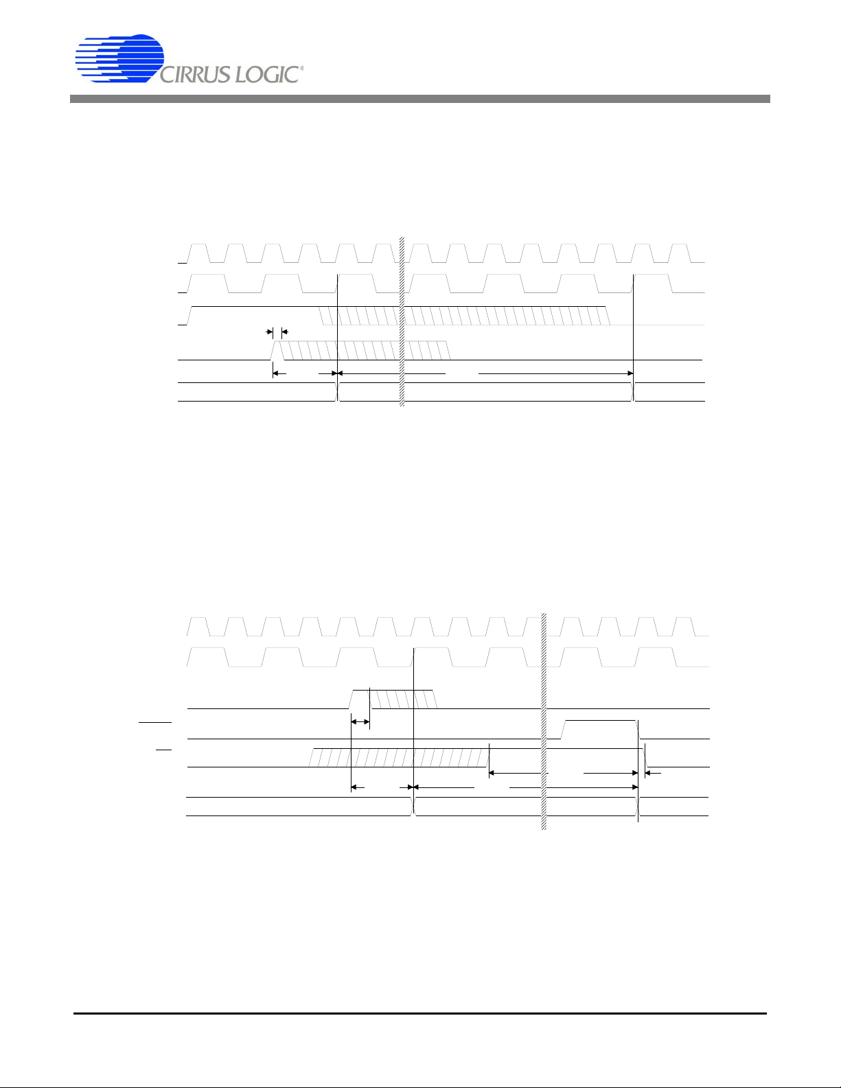
t
ccw
XIN
Calibration StandbyStandby
t
scl
t
cal
XIN/2
STATE
CAL
CONV
Figure 1. Calibration Timing (Not to Scale)
XIN
XIN/2
t
buh
Conversion StandbyStandby
CONV
STATE
t
scn
t
con
DRDY
BP/UP
t
bus
t
cpw
Figure 2. Conversion Timing (Not to Scale)
6 DS125F3
Page 7
CS5509
5V SWITCHING CHARACTERISTICS (T
0V, Logic 1 = VD+; C
= 50 pF) (Note 2)
L
= 25 °C; VA+, VD+ = 5V ±5%; Input Levels: Logic 0 =
A
Parameter Symbol Min Typ Max Unit
Serial Clock
Serial Clock Pulse Width High
Pulse Width Low
Access Time CS
Low to data valid (Note 16)
f
t
t
sclk
ph
t
pl
csd
0-2.5MHz
200
200
-
-
-
-
ns
ns
-60200ns
Maximum Delay Time (Note 17)
t
t
t
dd
fd1
fd2
-150310ns
-
-
60
160
150
300
ns
ns
SCLK falling to new SDATA bit
Output Float Delay CS
High to output Hi-Z (Note 18)
SCLK falling to Hi-Z
Notes: 16. If CS is activated asynchronously to DRDY, CS will not be recognized if it occurs when DRDY is high
for 2 clock cycles. The propagation delay time may be as great a s 2 f
proper clocking of SDATA when using asynchronous CS
2 f
+ 200 ns after CS goes low.
clk
, SCLK(i) should not be taken high sooner than
cycles plus 200 ns. To guarantee
clk
17. SDATA transitions on the falling edge of SCLK. Note that a rising SCLK must occur to enable the serial
port shifting mechanism before falling edges can be recognized.
18. If CS
is returned high before all data bits are output, the SDATA output will complete the current data
bit and then go to high impedance.
3.3V SWITCHING CHARACTERISTICS (T
Levels: Logic 0 = 0V, Logic 1 = VD+; C
= 50 pF) (Note 2)
L
= 25 °C; VA+ = 5V ±5%; VD+ = 3.3V ±5%; Input
A
Parameter Symbol Min Typ Max Unit
Serial Clock
Serial Clock Pulse Width High
Pulse Width Low
Access Time CS
Low to data valid (Note 16)
Maximum Delay Time (Note 17)
SCLK falling to new SDATA bit
Output Float Delay CS
High to output Hi-Z (Note 18)
SCLK falling to Hi-Z
f
t
t
t
t
t
sclk
ph
t
pl
csd
dd
fd1
fd2
0 - 1.25 MHz
200
200
-
-
-
-
ns
ns
-100200ns
-400600ns
-
-
70
320
150
500
ns
ns
DS125F3 7
Page 8
CS5509
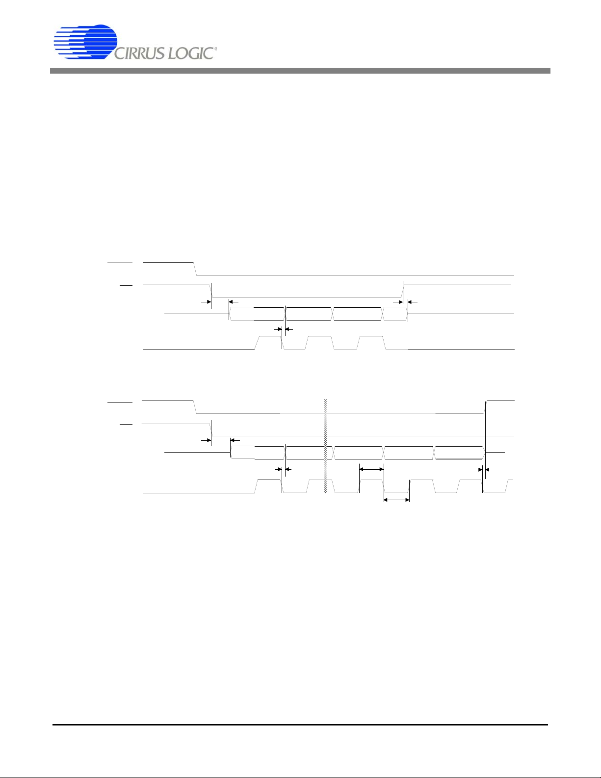
SCLK(i)
MSB-1MSB MSB-2SDATA(o) Hi-Z
MSB-1MSB LSB+2 LSB+1 LSB
SCLK(i)
SDATA(o) Hi-Z
t
fd1
t
csd
t
dd
t
ph
t
pl
t
dd
t
csd
CS
CS
DRDY
DRDY
t
fd2
Figure 3. Timing Relationships (Not to Scale)
8 DS125F3
Page 9

CS5509
RECOMMENDED OPERATING CONDITIONS (DGND = 0V) (Note 19)
Parameter Symbol Min Typ Max Unit
DC Power Supplies Positive Digital
Positive Analog
Analog Reference Voltage (Note 20)
Analog Input Voltage (Note 6)
Unipolar
Bipolar
Notes: 19. All voltages with respect to ground.
20. The CS5509 can be operated with a reference voltage as low as 100 mV; but with a corresponding
reduction in noise-free resolution. The common mode voltage of the voltage r eference may be any value
as long as +VREF and -VREF remain inside the supply values of VA+ and GND.
ABSOLUTE MAXIMUM RATINGS*
Parameter Symbol Min Typ Max Unit
DC Power Supplies Ground (Note 21)
Positive Digital (Note 22)
Positive Analog
Input Current, Any Pin Except Supplies (Notes 23 and 24)
Output Current
Power Dissipation (Total) (Note 25) - - 500 mW
Analog Input Voltage AIN and VREF pins
Digital Input Voltage
Ambient Operating Temperature
Storage Temperature
VD+
VA+
(VREF+) -
(VREF-) 1.0 2.5 3.6 V
VAIN
VAIN
-((VREF+) - (VREF-))--
3.15
4.75
0
GND
VD+
VA+
I
V
V
T
I
in
out
INA
IND
T
stg
5.0
5.0
(VREF+) - (VREF-)
(VREF+) - (VREF-)
-0.3
-0.3
-0.3
--±10mA
--±25mA
-0.3 - (VA+)+0.3 V
-0.3 - (VD+)+0.3 V
A
-40 - 85 °C
-65 - 150 °C
-
-
-
5.5
5.5
(VD+)-0.3
6.0
6.0
V
V
V
V
V
V
V
Notes: 21. No pin should go more positive than (VA+) + 0.3 V.
22. VD+ must always be less than (VA+) + 0.3 V, and can never exceed +6.0 V.
23. Applies to all pins including continuous overvoltage conditions at the analog input (AIN) pin.
24. Transient currents of up to 100 mA will not cause SCR latch-up. Maximum input current for a power
supply pin is ± 50 mA.
25. Total power dissipation, including all input currents and output currents.
*WARNING:Operation at or beyond these limits may result in permanent damage to the device.
Normal operation is not guaranteed at these extremes.
DS125F3 9
Page 10

CS5509
GENERAL DESCRIPTION
The CS5509 is a low power, 16-bit, monolithic
CMOS A/D converter designed specifically for
measurement of dc signals. The CS5509 includes a
delta-sigma charge-balance converter, a voltage
reference, a calibration microcontroller with
SRAM, a digital filter and a serial interface.
The CS5509 is optimized to operate from a 32.768
kHz crystal but can be driven by an external clock
whose frequency is between 30kHz and 330kHz.
When the digital filter is operated with a 32.768
kHz clock, the filter has zeros precisely at 50 and
60 Hz line frequencies and multiples thereof.
The CS5509 uses a "start convert" command to
start a convolution cycle on the digital filter. Once
the filter cycle is completed, the output port is updated.When operated with a 32.768kHz clock the
ADC converts and updates its output port at 20
samples/sec.The output port operates in a synchronous externally-clocked interface format.
THEORY OF OPERATION
Basic Converter Operation
The CS5509 A/D converter has three operating
states. These are stand-by, calibration, and conversion. When power is first applied, an internal power-on reset delay of about 10 ms resets all of the
logic in the device. The oscillator must then begin
oscillating before the device can be considered
functional. After the power-on reset is applied, the
device enters the wake-up period for 1800 clock
cycles after clock is present. This allows the deltasigma modulator and other circuitry (which are operating with very low currents) to reach a stable
bias condition prior to entering into either the calibration or conversion states. During the 1800 cycle
wake-up period, the device can accept an input
command. Execution of this command will not occur until the complete wake-up period elapses. If
no command is given, the device enters the standby
state.
Calibration
After the initial application of power, the CS5509
must enter the calibration state prior to performing
accurate conversions. During calibration, the chip
executes a two-step process. The device first performs an offset calibration and then follows this
with a gain calibration. The two calibration steps
determine the zero reference point and the full scale
reference point of the converter's transfer function.
From these points it calibrates the zero point and a
gain slope to be used to properly scale the output
digital codes when doing conversions.
The calibration state is entered whenever the CAL
and CONV pins are high at the same time. The state
of the CAL and CONV pins at power-on are recognized as commands, but will not be executed until
the end of the 1800 clock cycle wake-up period.
If CAL and CONV become active (high) during the
1800 clock cycle wake-up time, the converter will
wait until the wake-up period elapses before executing the calibration. If the wake-up time has
elapsed, the converter will be in the standby mode
waiting for instruction and will enter the calibration
cycle immediately if CAL and CONV become active. The calibration lasts for 3246 clock cycles.
Calibration coefficients are then retained in the
SRAM (static RAM) for use during conversion.
The state of BP/UP is ignored during calibration
but should remain stable throughout the calibration
period to minimize noise.
When conversions are performed in unipolar mode
or in bipolar mode, the converter uses the same calibration factors to compute the digital output code.
The only difference is that in bipolar mode the onchip microcontroller offsets the computed output
word by a code value of 8000H. This means that the
bipolar measurement range is not calibrated from
full scale positive to full scale negative. Instead it is
calibrated from the bipolar zero scale point to full
scale positive. The slope factor is then extended below bipolar zero to accommodate the negative in-
10 DS125F3
Page 11

CS5509
put signals. The converter can be used to convert
both unipolar and bipolar signals by changing the
BP/UP pin. Recalibration is not required when
switching between unipolar and bipolar modes.
At the end of the calibration cycle, the on-chip microcontroller checks the logic state of the CONV
signal. If the CONV input is low the device will enter the standby mode where it waits for further instruction. If the CONV signal is high at the end of
the calibration cycle, the converter will enter the
conversion state and perform a conversion on the
input channel. The CAL signal can be returned low
any time after calibration is initiated. CONV can
also be returned low, but it should never be taken
low and then taken back high until the calibration
period has ended and the converter is in the standby
state. If CONV is taken low and then high again
with CAL high while the converter is calibrating,
the device will interrupt the current calibration cycle and start a new one. If CAL is taken low and
CONV is taken low and then high during calibration, the calibration cycle will continue as the conversion command is disregarded. The state of
BP/UP is not important during calibrations.
If an "end of calibration" signal is desired, pulse the
CAL signal high while leaving the CONV signal
high continuously. Once the calibration is completed, a conversion will be performed. At the end of
the conversion, DRDY will fall to indicate the first
valid conversion after the calibration has been
completed.
The BP/UP pin is not a latched input. The BP/UP
pin controls how the output word from the digital
filter is processed. In bipolar mode the output word
computed by the digital filter is offset by 8000H
(see Understanding Converter Calibration). BP/UP
can be changed after a conversion is started as long
as it is stable for 82 clock cycles of the conversion
period prior to DRDY falling. If one wishes to intermix measurement of bipolar and unipolar signals
on various input signals, it is best to switch the
BP/UP pin immediately after DRDY falls and
leave BP/UP
The digital filter in the CS5509 has a Finite Impulse Response and is designed to settle to full accuracy in one conversion time.
If CONV is left high, the CS5509 will perform continuous conversions. The conversion time will be
1622 clock cycles. If conversion is initiated from
the standby state, there may be up to two XIN clock
cycles of uncertainty as to when conversion actually begins. This is because the internal logic operates at one half the external clock rate and the exact
phase of the internal clock may be 180° out of
phase relative to the XIN clock. When a new conversion is initiated from the standby state, it will
take up to two XIN clock cycles to begin. Actual
conversion will use 1624 clock cycles before
DRDY
been updated. See the Serial Interface Logic section of the data sheet for information on reading
data from the serial port.
stable until DRDY falls again.
goes low to indicate that the serial port has
Conversion
The conversion state can be entered at the end of
the calibration cycle, or whenever the converter is
idle in the standby mode. If CONV is taken high to
initiate a calibration cycle ( CAL also high), and remains high until the calibration cycle is completed
(CAL is taken low after CONV transitions high),
the converter will begin a conversion upon completion of the calibration period.
DS125F3 11
In the event the A/D conversion command (CONV
going positive) is issued during the conversion
state, the current conversion will be terminated and
a new conversion will be initiated.
Voltage Reference
The CS5509 uses a differential voltage reference
input. The positive input is VREF+ and the negative input is VREF-. The voltage between VREF+
and VREF- can range from 1 volt minimum to 3.6
volts maximum. The gain slope will track changes
Page 12

CS5509
FFFF
FFFE
--------------- -
8000
7FFF
-------------- -
0001
0000
------------ -
in the reference without recalibration, accommodating ratiometric applications.
Analog Input Range
The analog input range is set by the magnitude of
the voltage between the VREF+ and VREF- pins.
In unipolar mode the input range will equal the
magnitude of the voltage reference. In bipolar
mode the input voltage range will equate to plus
and minus the magnitude of the voltage reference.
While the voltage reference can be as great as 3.6
volts, its common mode voltage can be any value as
long as the reference inputs VREF+ and VREFstay within the supply voltages VA+ and GND.
The differential input voltage can also have any
common mode value as long as the maximum signal magnitude stays within the supply voltages.
The A/D converter is intended to measure dc or low
frequency inputs. It is designed to yield accurate
conversions even with noise exceeding the input
voltage range as long as the spectral components of
this noise will be filtered out by the digital filter.
For example, with a 3.0 volt reference in unipolar
mode, the converter will accurately convert an input dc signal up to 3.0volts with up to 15% overrange for 60Hz noise. A 3.0volt dc signal could
have a 60Hz component which is 0.5volts above
the maximum input of 3.0 (3.5 volts peak; 3.0 volts
dc plus 0.5 volts peak noise) and still accurately
convert the input signal (XIN = 32.768 kHz). This
assumes that the signal plus noise amplitude stays
within the supply voltages.
The CS5509 converters output data in binary format when converting unipolar signals and in offset
binary format when converting bipolar signals. Table 1 outlines the output coding for both unipolar
and bipolar measurement modes.
Converter Performance
The CS5509 A/D converter has excellent linearity
performance. Calibration minimizes the errors in
Unipolar Input
Voltage
> (VREF - 1.5 LSB)
VREF - 1.5 LSB VREF - 1.5 LSB
VREF/2 - 0.5 LSB -0.5 LSB
+0.5 LSB -VREF + 0.5 LSB
< (+0.5 LSB)
Note: T able excludes commo n mode voltage on the
signal and reference inputs.
Table 1. Output Coding
Output
Codes
FFFF
0000
Bipolar Input
Voltage
> (VREF - 1.5 LSB)
< (-VREF + 0.5 LSB)
offset and gain. The CS5509 device has no missing
code performance to 16-bits. Figure4 illustrates the
DNL of the CS5509. The converter achieves Common Mode Rejection (CMR) at dc of 105dB typical, and CMR at 50 and 60Hz of 120dB typical.
The CS5509 can experience some drift as temperature changes. The CS5509 uses chopper-stabilized
techniques to minimize drift. Measurement errors
due to offset or gain drift can be eliminated at any
time by recalibrating the converter.
Analog Input Impedance Considerations
The analog input of the CS5509 can be modeled as
illustrated in Figure 5. Capacitors (15 pF each) are
used to dynamically sample each of the inputs
(AIN+ and AIN-). Every half XIN cycle the switch
alternately connects the capacitor to the output of
the buffer and then directly to the AIN pin. Whenever the sample capacitor is switched from the output of the buffer to the AIN pin, a small packet of
charge (a dynamic demand of current) is required
from the input source to settle the voltage of the
sample capacitor to its final value. The voltage on
the output of the buffer may differ up to 100 mV
from the actual input voltage due to the offset voltage of the buffer. Timing allows one half of a XIN
clock cycle for the voltage on the sample capacitor
to settle to its final value.
12 DS125F3
Page 13

CS5509
Figure 4. CS5509 Differential Nonlinearity Plot
+
15 pF
V
os
≤
100 mV
+
V
os
≤
100 mV
Internal
Bias
Voltage
15 pF
AIN+
AIN-
-
-
Figure 5. Analog Input Model
Rs
max
1–
2XIN 15pF C
EXT
+()
V
e
V
e
15pF 100mV()
15pF C
EXT
+
-------------------------------------+
---------------------------------------------------
ln
-------------------------------------------------------------------------------------------------------------------------=
The VREF+ and VREF- inputs have nearly the
same structure as the AIN+ and AIN- inputs.
Therefore, the discussion on analog input impedance applies to the voltage reference inputs as well.
Digital Filter Characteristics
The digital filter in the CS5509 is the combination
of a comb filter and a low pass filter. The comb filter has zeros in its transfer function which are optimally placed to reject line interference frequencies
(50 and 60 Hz and their multiples) when the
CS5509 is clocked at 32.768 kHz. Figures 6, 7 and
An equation for the maximum acceptable source
resistance is derived.
This equation assumes that the offset voltage of the
buffer is 100 mV, which is the worst case. The value of Ve is the maximum error voltage which is acceptable. C
is the combination of any external
EXT
or stray capacitance.
For a maximum error voltage (Ve) of 10 µV in the
CS5509 (1/4LSB at 16-bits), the above equation indicates that when operating from a 32.768 kHz
XIN, source resistances up to 110 kΩ are acceptable in the absence of external capacitance
(C
DS125F3 13
=0).
EXT
8 illustrate the magnitude and phase characteristics
of the filter. Figure 6 illustrates the filter attenuation from dc to 260 Hz. At exactly 50, 60, 100, and
120 Hz the filter provides over 120 dB of rejection.
Table 2 indicates the filter attenuation for each of
the potential line interference frequencies when the
converter is operating with a 32.768 kHz clock.
The converter yields excellent attenuation of these
interference frequencies even if the fundamental
line frequency should vary ± 1% from its specified
frequency. The -3 dB corner frequency of the filter
when operating from a 32.768 kHz clock is 17 Hz.
Figure 8 illustrates that the phase characteristics of
the filter are precisely linear phase.
If the CS5509 is operated at a clock rate other than
32.768kHz, the filter characteristics, including the
comb filter zeros, will scale with the operating
clock frequency. Therefore, optimum rejection of
Page 14

CS5509
0
0
40
402.8380805.66
120
1208.5
160
1611.3
200
2014.2
240
2416.9
Frequency (Hz)
-160
-140
-120
-100
-80
-60
-40
-20
0
Atte nua tion (d B)
XIN = 32.768 kHz
X1
X2
X1 = 32.768kHz
X2 = 330.00kHz
Figure 6. Filter Magnitude Plot to 260 Hz
0 5
10 15 20 25 30 35 40 45 50
Frequency (Hz)
-140
-120
-100
-80
-60
-40
-20
0
Attenuation (dB)
Flatness
dB
-0.010
-0.041
-0.093
-0.166
-0.259
-0.510
-0.667
-0.846
-1.047
-3.093
1
2
3
4
5
6
7
8
9
10
17
XIN = 32.768 kHz
Frequency
-0.374
Figure 7. Filter Magnitude Plot to 50 Hz
05
10 15 20 25 30 35 40 45 50
Frequency (Hz)
-180
-135
-90
-45
0
45
90
135
180
Phase (Degrees)
XIN = 32.768 kHz
Figure 8. Filter Phase Plot to 50 Hz
line frequency interference will occur with the
CS5509 running at 32.768kHz.
14 DS125F3
Frequency
(Hz)
50
Notch
Depth
(dB)
125.6
Frequency
(Hz)
Minimum
Attenuation
50 ±1% 55.5
(dB)
60 126.7 60 ±1% 58.4
100 145.7 100 ±1% 62.2
120 136.0 120 ±1% 68.4
150
180
200
240
T able 2. Filter Notch Attenuation (XIN = 32.768 kHz)
118.4
132.9
102.5
108.4
150 ±1% 74.9
180 ±1% 87.9
200 ±1% 94.0
240 ±1% 104.4
Anti-Alias Considerations for Spectral Measurement Applications
Input frequencies greater than one half the output
word rate (CONV = 1) may be aliased by the converter. To prevent this, input signals should be limited in frequency to no greater than one half the
output word rate of the converter (when CONV
=1). Frequencies close to the modulator sample rate
(XIN/2) and multiples thereof may also be aliased.
If the signal source includes spectral components
above one half the output word rate (when CONV
= 1) these components should be removed by
means of low-pass filtering prior to the A/D input
Page 15

CS5509
to prevent aliasing. Spectral components greater
than one half the output word rate on the VREF inputs (VREF+ and VREF-) may also be aliased. Filtering of the reference voltage to remove these
spectral components from the reference voltage is
desirable.
Crystal Oscillator
The CS5509 is designed to be operated using a
32.768kHz "tuning fork" type crystal. One end of
the crystal should be connected to the XIN input.
The other end should be attached to XOUT. Short
lead lengths should be used to minimize stray capacitance.
Over the industrial temperature range (-40 to
+85 °C) the on-chip gate oscillator will oscillate
with other crystals in the range of 30kHz to 53 kHz.
The chip will operate with external clock frequencies from 30kHz to 330kHz over the industrial temperature range. The 32.768 kHz crystal is normally
specified as a time-keeping crystal with tight specifications for both initial frequency and for drift
over temperature. To maintain excellent frequency
stability, these crystals are specified only over limited operating temperature ranges (i.e. -10 °C to
+60 °C) by the manufacturers. Applications of
these crystals with the CS5509 does not require
tight initial tolerance or low tempco drift. Therefore, a lower cost crystal with looser initial tolerance and tempco will generally be adequate for use
with the CS5509. Also check with the manufacturer about wide temperature range application of
their standard crystals. Generally, even those crystals specified for limited temperature range will operate over much larger ranges if frequency stability
over temperature is not a requirement. The frequency stability can be as bad as ±3000 ppm over the
operating temperature range and still be typically
better than the line frequency (50 Hz or 60Hz) stability over cycle-to-cycle during the course of a
day.
Serial Interface Logic
The digital filter in the CS5509 takes 1624 clock
cycles to compute an output word once a conversion begins. At the end of the conversion cycle, the
filter will attempt to update the serial port. Two
clock cycles prior to the update DRDY will go
high. When DRDY goes high just prior to a port update it checks to see if the port is either empty or
unselected (CS = 1). If the port is empty or unselected, the digital filter will update the port with a
new output word. When new data is put into the
port DRDY will go low.
Reading Serial Data
SDATA is the output pin for the serial data. When
CS goes low after new data becomes available
(DRDY goes low), the SDATA pin comes out of
Hi-Z with the MSB data bit present. SCLK is the
input pin for the serial clock. If the MSB data bit is
on the SDATA pin, the first rising edge of SCLK
enables the shifting mechanism. This allows the
falling edges of SCLK to shift subsequent data bits
out of the port. Note that if the MSB data bit is output and the SCLK signal is high, the first falling
edge of SCLK will be ignored because the shifting
mechanism has not become activated. After the
first rising edge of SCLK, each subsequent falling
edge will shift out the serial data. Once the LSB is
present, the falling edge of SCLK will cause the
SDATA output to go to Hi-Z and DRDY
high. The serial port register will be updated with a
new data word upon the completion of another conversion if the serial port has been emptied, or if the
CS is inactive (high).
CS
can be operated asynchronously to the DRDY
signal. The DRDY signal need not be monitored as
long as the CS signal is taken low for at least two
XIN clock cycles plus 200ns prior to SCLK being
toggled. This ensures that CS has gained control
over the serial port.
to return
DS125F3 15
Page 16

CS5509
Power Supplies and Grounding
The analog and digital supply pins to the CS5509
are brought out on separate pins to minimize noise
coupling between the analog and digital sections of
the chip. In the digital section of the chip the supply
current flows into the VD+ pin and out of the GND
pin. As a CMOS device, the CS5509 requires that
the supply voltage on the VA+ pin always be more
positive than the voltage on any other pin of the device. If this requirement is not met, the device can
latch-up or be damaged. In all circumstances the
VA+ voltage must remain more positive than the
VD+ or GND pins; VD+ must remain more positive than the GND pin.
Figure 9a illustrates the System Connection Diagram for the CS5509. Note that all supply pins are
bypassed with 0.1 µF capacitors and that the VD+
digital supply is derived from the VA+ supply. Figure 9b illustrates the CS5509 operating from a +5V
analog supply and +3.3V digital supply.
When using separate supplies for VA+ and VD+,
VA+ must be established first. VD+ should never
become more positive than VA+ under any operating condition. Remember to investigate transient
power-up conditions, when one power supply may
have a faster rise time.
16 DS125F3
Page 17

CS5509
CS5509
+5V
Analog
Supply
VD+VA+
VREF+
VREF-
GND
0.1 µF 0.1 µF
8
7
9
10
11
12
13
+
-
Analog
Signal
AIN+
AIN-
SCLK
SDATA
14
15
XIN
XOUT
16
DRDY
CAL
3
1
CS
CONV
2
6
BP/UP
4
5
32.768 kHz
10
Ω
Voltage
Reference
Optional
Clock
Source
Serial
Data
Interface
Control
Logic
Figure 9a. System Connection Diagram Using a Single Supply
DS125F3 17
Page 18

CS5509
CS5509
+5V
Analog
Supply
VD+VA+
VREF+
VREF-
GND
0.1 µF 0.1 µF
8
7
9
10
11
12
13
+
-
Analog
Signal
AIN+
AIN-
SCLK
SDATA
14
15
XIN
XOUT
16
DRDY
CAL
3
1
CS
CONV
2
6
BP/UP
4
5
32.768 kHz
Voltage
Reference
Optional
Clock
Source
Serial
Data
Interface
Control
Logic
+3.3V to +5V
Digital
Supply
Note: VD+ must never be more positive than VA+
Figure 9b. System Connection Diagram Using Split Supplies
18 DS125F3
Page 19
PIN DESCRIPTIONS*
1
2
3
4
5
6
7
8
9
10
11
12
13
14
15
16
DRDY
SDATA
SCLK
VD+
GND
VA+
VREFVREF+AIN-
AIN+
BP/UP
XOUT
XIN
CAL
CONV
CS
DIFFERENTIAL ANALOG INPUT
DIFFERENTIAL ANALOG INPUT
BIPOLAR / UNIPOLAR
CRYSTAL OUT
CRYSTAL IN
CALIBRATE
CONVERT
CHIP SELECT DATA READY
SERIAL DATA OUTPUT
SERIAL CLOCK INPUT
POSITIVE DIGITAL POWER
GROUND
POSITIVE ANALOG POWER
VOLTAGE REFERENCE INPUT
VOLTAGE REFERENCE INPUT
* Pinout applies to both PDIP and SOIC
Clock Generator
CS5509
XIN; XOUT - Crystal In; Crystal Out, Pins 4, 5.
A gate inside the chip is connected to these pins and can be used with a crystal to provide the
master clock for the device. Alternatively, an external (CMOS compatible) clock can be
supplied into the XIN pin to provide the master clock for the device. Loss of clock will put the
device into a lower powered state (approximately 70% power reduction).
Serial Output I/O
CS - Chip Select, Pin 1.
This input allows an external device to access the serial port.
DRDY - Data Ready, Pin 16.
Data Ready goes low at the end of a digital filter convolution cycle to indicate that a new
output word has been placed into the serial port. DRDY
shifted out of the serial port or two master clock cycles before new data becomes available if
the CS pin is inactive (high).
SDATA - Serial Data Output, Pin 15.
SDATA is the output pin of the serial output port. Data from this pin will be output at a rate
determined by SCLK. Data is output MSB first and advances to the next data bit on the falling
edges of SCLK. SDATA will be in a high impedance state when not transmitting data.
SCLK - Serial Clock Input, Pin 14.
DS125F3 19
A clock signal on this pin determines the output rate of the data from the SDATA pin. This pin
must not be allowed to float.
will return high after all data bits are
Page 20

Control Input Pins
CAL - Calibrate, Pin 3.
When taken high the same time that the CONV pin is taken high the converter will perform a
self-calibration which includes calibration of the offset and gain scale factors in the converter.
CONV - Convert, Pin 2.
The CONV pin initiates a calibration cycle if it is taken from low to high while the CAL pin is
high, or it initiates a conversion if it is taken from low to high with the CAL pin low. If CONV
is held high (CAL low) the converter will do continuous conversions.
BP/UP - Bipolar/Unipolar, Pin 6.
CS5509
The BP/UP
convert bipolar input signals; when low it will convert unipolar input signals.
Measurement and Reference Inputs
AIN+, AIN- - Differential Analog Inputs, Pins 7, 8.
Analog differential inputs to the delta-sigma modulator.
VREF+, VREF- - Differential Voltage Reference Inputs, Pins 9, 10.
A differential voltage reference on these pins operates as the voltage reference for the
converter. The voltage between these pins can be any voltage between 1.0 and 3.6 volts.
Power Supply Connections
VA+ - Positive Analog Power, Pin 11.
Positive analog supply voltage. Nominally +5 volts.
VD+ - Positive Digital Power, Pin 13.
Positive digital supply voltage. Nominally +5 volts or +3.3 volts.
pin selects the conversion mode of the converter. When high the converter will
GND - Ground, Pin 12.
Ground.
20 DS125F3
Page 21

SPECIFICATION DEFINITIONS
Linearity Error
The deviation of a code from a straight line which connects the two endpoints of the A/D
Converter transfer function. One endpoint is located 1/2 LSB below the first code transition and
the other endpoint is located 1/2 LSB beyond the code transition to all ones. Units in percent of
full-scale.
Differential Nonlinearity
The deviation of a code's width from the ideal width. Units in LSBs.
Full Scale Error
The deviation of the last code transition from the ideal [{(VREF+) - (VREF-)} - LSB]. Units
are in LSBs.
Unipolar Offset
The deviation of the first code transition from the ideal ( LSB above the voltage on the AINpin.) when in unipolar mode (BP/UP low). Units are in LSBs.
CS5509
Bipolar Offset
The deviation of the mid-scale transition (011...111 to 100...000) from the ideal ( LSB below
the voltage on the AIN- pin.) when in bipolar mode (BP/UP high). Units are in LSBs
DS125F3 21
Page 22

PACKAGE DIMENSIONS
SOIC
MILLIMETERS
INCHES
MIN MAX
MAX
MIN
0.095
0.105
2.41
2.67
0.008
0.015
0.203
0.381
0.398
0.420
10.11
10.67
0.0200.013
0.51
0.33
0.016
0.035
0.41
0.89
8°0°
0°
8°
MILLIMETERS
INCHES
MIN
MAX MAX
MIN
pins
0.410
0.390
9.91
10.41
16
0.510
0.490
12.45
12.95
20
0.610
0.590
14.99
15.50
24
0.710
0.690
17.53
18.03
28
0.0120.0050.127 0.300
1.14
0.040
DIM
E
E
b
L
D
e
A
A
c
0.292 0.298
7.42
7.57
D
E
E
1
e
A
A
b
1
A
2
c
L
µ
1
µ
1
1.40
0.055
A
2
see table above
NOM
2.54
0.280
10.41
0.46
-
-
NOM
10.16
12.70
15.24
17.78
-
7.49
1.27
2.29
2.542.41
NOM
0.100
0.011
0.410
0.018
-
-
NOM
0.400
0.500
0.600
0.700
-
0.295
0.050
0.1000.090 0.095
CS5509
22 DS125F3
Page 23

ENVIRONMENTAL, MANUFACTURING, & HANDLING INFORMATION
Model Peak Relfow Temp MSL Rating* Maximum Floor Life
CS5509-ASZ (lead free) 260 °C 3 7 Days
* MSL (Moisture Sensitivity Level) as specified by IPC/JEDEC J-STD-020.
CS5509
DS125F3 23
Page 24

REVISION HISTORY
Contacting Cirrus Logic Support
For all product questions and inquiries contact a Cirrus Logic Sales Representative.
To find the one nearest to you go to www.cirrus.com
IMPORTANT NOTICE
Cirrus Logic, Inc. and its subsidiaries (“Cirrus”) believe that the informati on contained in this document is accurate and reliable. However, the information is subject
to change without noti ce and is provide d “AS IS” wi thout wa rranty o f any ki nd (expre ss or impl ied). Cu stomers ar e advised to obtain the latest version of relevant
information to verify, before placing orders, that information being relied on is current and complete. All products are sold subject to the terms and conditions of sale
supplied at the time of order acknowledg ment, including those pe rtaining to warranty, ind emnification, an d limitation of liabili ty. No responsibility is assumed by Cirrus
for the use of this information, including use of this information as the basis for manufacture or sale of any items, or for infringement of patents or other rights of third
parties. This document is the property of Cirrus and by furnishing this inform atio n, Cirrus gr ants no license , express or implied under any patents, mask work rights,
copyrights, trademarks, trade secrets or other intellectual p roperty rights. Cirrus owns the cop yrights associated with the informatio n contained herein and gives consent for copies to be made of the information only for use within your organization with respect to Cirrus integrated circuits or other products of Cirrus. This consent
does not extend to other copying such as copying for general distribution, advertising or promotional purposes, or for creating any work for resale.
CERTAIN APPLICATIONS USING SEMICONDUCT OR PRODUCT S MAY I NVOL VE POTE NTI A L RISK S OF DEATH, PE RS ONAL IN JURY , OR SE VERE PROPERTY OR ENVIRONMENTAL DAMAGE (“CRITICAL APPLICATIONS”). CIRRUS PRODUCTS ARE NOT DESIGNED, AUTHORIZED OR WARRANTED FOR USE
IN PRODUCTS SURGICALLY IMPLANTED INTO THE BODY, AUTOMOTIVE SAFETY OR SECURITY DEVICES, LIFE SUPPORT PRODUCTS OR OTHER CRITICAL APPLICATIONS. INCLUSION OF CIRRUS PRODUCTS IN SUCH APPLICATIONS IS UNDERSTOOD TO BE FULLY AT THE CUSTOMER'S RI SK AND
CIRRUS DISCLAIMS AND MAKES NO WARRANTY, EXPRESS, STATUTORY OR IMPLIED, INCLUDING THE IMPLIED WARRANTIES OF MERCHANTABILITY
AND FITNESS FOR PARTICULAR PURPOSE, WITH REGARD TO ANY CIRRUS PRODUCT THAT IS USED IN SUCH A MANNER. IF THE CUSTOMER OR
CUSTOMER'S CUSTOMER USES OR PERMITS THE USE OF CIRRUS PRODUCTS IN CRITICAL APPLICATIONS, CUSTOMER AGREES, BY SUCH USE, TO
FULLY INDEMNIFY CIRRUS, I TS OFFICERS, DIRECTORS, EMPLOYEES, DIST RIBUT ORS AN D OTHE R AGENTS FRO M ANY A ND ALL LI ABILITY, INCLUDING ATTORNEYS' FEES AND COSTS, THAT MAY RESULT FROM OR ARISE IN CONNECTION WITH THESE US ES .
Cirrus Logic, Cirrus, and the Cirrus Logic logo designs are tradem arks of Cirr us Log ic, Inc. All other brand an d prod uct nam es in this do cum ent m ay be tradem ar ks
or service marks of their respective owners.
Revision Date Changes
F1 Aug ‘97 First “final” release.
F2 Aug ‘05 Added lead-free device ordering info. Added legal notice. Added MSL data.
F3 Jul ‘09 Removed PDIP and leaded (Pb) devices from ordering information.
CS5509
24 DS125F3
 Loading...