

Page 1
CS5505/6/7/8
Copyright Cirrus Logic, Inc. 2009
(All Rights Reserved)
http://www.cirrus.com
CS5505/6/7/8
Very Low Power, 16-bit & 20-bit A/D Converters
OCT ‘09
DS59F7
Very Low Power, 16-Bit and 20-Bit A/D Converters
Features
Description
l Very Low Power Consumption
- Single supply +5 V operation: 1.7 mW
- Dual supply ±5 V operation: 3.2 mW
l Offers superior performance to VFCs and
multi-slope integrating ADCs
l Differential Inputs
- Single-channel (CS5507/8) and Four-channel
(CS5505/6) pseudo-differential versions
l Either 5 V or 3.3 V Digital Interface
l Linearity Error:
- ±0.0015% FS (16-bit CS5505/7)
- ±0.0007% FS (20-bit CS5506/8)
l Output update rates up to 100 Sps
l Flexible Serial Port
l Pin-Selectable Unipolar/Bipolar Ranges
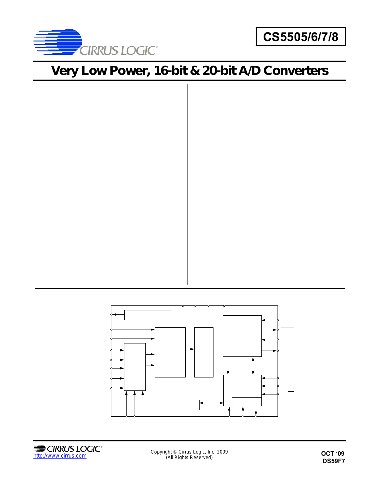
I
The CS5505/6/7/8 are a family of low power CMOS A/D
converters which are ideal for measuring low-frequency
signals representing physical, chemical, and biological
processes.
The CS 5507/8 have single-channel differential anal
og
and reference inputs while the CS5505/6 have four
pseudo-differ
ential analog input channels. The
CS5505/7 have a 16-bit output word. The CS5506/8
have a 20-bit output word.The CS5505/6/7/8 sample
ommand up to 100 Sps
upon c
.
The on-chip digital filter offers superior li ne rejection at
50 and 60 Hz when the device is operated from a
32.768 kHz clock (output word rate = 20 Sps).
The CS 5505/6/7/8 include on-chip self-calibration circuitry whi
ch c
an be initiated at any time or temperature
to ensure minimum offset and full-scale errors.
The CS5505/6/7/8 serial port offers two general-purpose
modes for the direct interface to shift r egisters or synchr
microcontroll
s serial ports of indust
onou
ers.
ry-standard
ORDERING INFORMATION
See page 30.
Cirrus Logic, Inc.
Crystal Semiconductor Products Division
P.O. Box 17847, Austin, Texas 78760
(512) 445 7222 FAX: (512) 445 7581
http://www.crystal.com
95()287
95()
95()
$,1
$,1
$,1
$,1
$,1
9ROWDJH5HIHUHQFH
08;
$$
'LIIHUHQWLDO
WK2UGHU
'HOWD6LJPD
0RGXODWRU
&DOLEUDWLRQ65$0
&6%,7$1'&6%,76+2:1
9$
9$
'LJLWDO
)LOWHU
Copyright © Cirrus Logic, Inc. 1997
'*1'9'
6HULDO
,QWHUIDFH
/RJLF
&DOLEUDWLRQµ&
26&
&219 ;,1
(All Rights Reserved)
;287
&6
'5'<
6&/.
6'$7$
06/3
&$/
%383
MAR ‘95
DS59F4
1
Page 2
CS5505/6/7/8
2 DS59F7
CS5505/6/7/8
ANALOG CHARACTERISTICS
±
3.3V
5%; VREF+ = 2.5V(external); VREF- = 0V; f
(TA = T
to T
MIN
= 32.768kHz; Bipolar Mode; R
CLK
; VA+ = 5V ± 10%; VA- = -5V ± 10%; VD+ =
MAX
= 1kΩ with a 10nF
source
to AGND at AIN; Anal og input channel AIN1+; AIN- = AGND; unless otherwise specified.) (Notes 1, 2)
CS5505/7-A CS5507-S
Parameter* Min Typ Max Min Typ Max Units
Specified Temperature Range -40 to +85 -55 to +125
°
C
Accuracy
Linearity Error - 0.0015 0.003 - 0.0015 0.003
Differential Nonlinearity -
Full Scale Error (Note 3) -
Full Scale Drift (Note 4) -
Unipolar Offset (Note 3) -
Unipolar Offset Drift (Note 4) -
Bipolar Offset (Note 3) -
Bipolar Offset Drift (Note 4) -
±
0.25
±
0.25
±
±
±
±
0.25
±
0.25
0.5
0.5
0.5
±
0.5
±
2
--
±
2
--
±
1
--
-
-
-
-
±
0.25
±
0.5
±
2
±
1
±
1
±
0.5
±
0.5
±
0.5
±
-LSB
±
-LSB
±
-LSB
±
%FS
LSB
16
LSB
LSB
LSB
16
16
16
16
16
16
2
4
2
Noise (Referred to Output) - 0.16 - - 0.16 - LSB-
rms
16
Notes: 1. The AIN pin presents a very high input resistance at dc and a minor dynamic load which scales to the
master clock frequency. Both sour ce resistance and shunt capacitance are therefore critical in
determining the CS5505/6/7/8’s source impedance requirements. For more information refer to the
text section
Analog Input Impedance Consi derations.
2. Specifications guaranteed by desi gn, characterization and/or test.
3. Applies after calibration at the temperature of interest.
4. Total drift over the specified temperature range since calibration at power-up at 25°C.
Recalibration at any temperature will remove these errors.
Unipolar Mode Bipolar Mode
mV LSB’s % FS ppm FS LSB’s % FS ppm FS
10 0.26 0.0004 4 0.13 0.0002 2
19 0.50 0.0008 8 0.26 0.0004 4
38 1.00 0.0015 15 0.50 0.0008 8
76 2.00 0.0030 30 1.00 0.0015 15
152 4.00 0.0061 61 2.00 0.0030 30
VREF = 2.5V
CS5505/7; 16-Bit Unit Conversion Factors
* Refer to the Specification Definitions immediately following the Pin Description Section.
Specifications are subject to change without notice.
2 DS59F7
Page 3
CS5505/6/7/8
DS59F7 3
CS5505/6/7/8
ANALOG CHARACTERISTICS
3.3V ± 5%; VREF+ = 2.5V (external); VREF- = 0V; f
(TA = T
to T
MIN
= 32.768kHz ; Bipolar Mode; R
CLK
; VA+ = 5V ± 10%; VA- = -5V ± 10%; VD+ =
MAX
source
= 1kΩ with a
10nF to AGND at AIN; Analog input channel AIN1+; AIN- = AGND; unless otherwise specified.) (Notes 1, 2)
CS5506/8-B CS5508-S
Parameter* Min Typ Max Min Typ Max Units
Specified Temperature Range -40 to +85 -55 to +125
°
Accuracy
Linearity Error - 0.0007 0.0015 - 0.0015 0.003
Differential Nonlinearity
±
%FS
Bits
(No Missing Codes) 20 - - 20 - -
Full Scale Error (Note 3) -
Full Scale Drift (Note 4) -
Unipolar Offset (Note 3) -
Unipolar Offset Drift (Note 4) -
Bipolar Offset (Note 3) -
Bipolar Offset Drift (Note 4) -
±
4
±
8
±
8
±
8
±
4
±
4
±
32
--
±
32
--
±
16
--
-
-
-
±
8
±
32
±
16
±
16
±
8
±
8
±
32
±
64
±
32
LSB
-LSB
LSB
-LSB
LSB
-LSB
Noise (Referred to Output) - 2.6 - - 2.6 - LSB-
rms
C
20
20
20
20
20
20
20
Unipolar Mode Bipolar Mode
mV LSB’s % FS ppm FS LSB’s % FS ppm FS
0.596 0.25 0.0000238 0.24 0.13 0.0000119 0.12
1.192 0.50 0.0000477 0.47 0.26 0.0000238 0.24
2.384 1.00 0.0000954 0.95 0.50 0.0000477 0.47
4.768 2.00 0.0001907 1.91 1.00 0.0000954 0.95
9.537 4.00 0.0003814 3.81 2.00 0.0001907 1.91
VREF = 2.5V
CS5506/8; 20-Bit Unit Conversion Factors
DYNAMIC CHARACTERISTICS
Parameter Symbol Ratio Units
f
Modulator Sampling Frequency f
Output Update Rate (CONV = 1) f
Filter Corner Frequency f
Settling Time to
1
⁄2 LSB (FS Step)
s
out
-3dB
t
s
/2 Hz
clk
f
/1622 Sps
clk
f
/1928 Hz
clk
1/f
out
s
DS59F7 3
Page 4
CS5505/6/7/8
4 DS59F7
CS5505/6/7/8
ANALOG CHARACTERISTICS
3.3V ± 5%; VREF+ = 2.5V (external); VREF- = 0V; f
10nF to AGND at AIN; Analog input channel AIN1+; AIN- = AGND; unless otherwise specified.) (Notes 1, 2)
Parameter* Min Typ Max Min Typ Max Units
Specified Temperature Range -40 to +85 -55 to +125
(TA = T
to T
MIN
= 32.768kHz ; Bipolar Mode; R
CLK
CS5505/7
CS5506/8 CS5507/8-S
; VA+ = 5V
MAX
±
10%; VA- = -5V ± 10%; VD+ =
= 1kΩ with a
source
°
Analog Input
Analog Input Range: Unipolar
(VAIN+)-(VAIN-) Bi polar (Note 5)
Common Mode Rejection: dc
50, 60 Hz (Note 6)-120
Off Channel Isolation - 120 - - 120 - dB
Input Capacitance - 15 - - 15 - pF
DC Bias Current (Note 1) - 5 - - 5 - nA
0 to +2.5
±
2.5
105
-
0 to +2.5
±
2.5
-
-
-
120
105
-
-
-
Volts
Volts
dB
dB
Voltage Reference (Output)
VREFOUT Voltage - (VA+)-2.5 - - (VA+)-2.5 - Volts
VREFOUT Voltage Tolerance - - 4.0 - - 4.0 %
C
VREFOUT Voltage Temperature Coefficient - 60 - - 60 -
VREFOUT Line Regulation - 1.5 - - 1.5 - mV/Volt
VREFOUT Output Voltage Noise
0.1 to 10 Hz
VREFOUT: Sour ce Current
Sink Current
-50- -50-
-
-
-
-
3
50
-
-
-
-
50
ppm/°C
µ
V
p-p
3
µ
A
µ
A
Power Supplies
DC Power Supply Currents: I
Power Dissipation: (Note 7)
SLEEP inactive
SLEEP active
Power Supply Rejection: Positive Supplies
Negative Supplies
Notes: 5. Common mode voltage may be at any value as long as AIN+ and AIN- remain within the VA+ and
VA- supply voltages.
6. XIN = 32.768 kHz. Guaranteed by design and / or characterization.
7. All outputs unloaded. Al l inputs CMOS levels. SLEEP mode controlled by M/SLP pin.
SLEEP active = M/SLP pin at (VD+)/2 input level.
Total
I
Analog
I
Digital
-
-
-
-
-
-
-
340
300
40
3.2
5
80
80
450
-
-
4.5
10
-
-
-
-
-
-
-
-
-
340
300
40
3.2
10
80
80
450
-
-
4.5
25
-
-
µ
A
µ
A
µ
A
mW
µ
W
dB
dB
4 DS59F7
Page 5
CS5505/6/7/8
DS59F7 5
CS5505/6/7/8
5V DIGITAL CHARACTERISTICS
(TA = T
MIN
to T
; VA+VD+ = 5V ± 10%; VA-= -5V ± 10%;
MAX
DGND = 0.) All measurements below are performed under static conditions. (Note 2)
Parameter Symbol Min Typ Max Units
High-Level Input Voltage: XIN
M/SLP
All Pins Except XIN and M/SLP
Low-Level Input Voltage: XIN
M/SLP
All Pins Except XIN and M/SLP
M/SLP SLEEP Active Threshold (Note 8) V
High-Level Output Voltage (Note 9) V
Low Level Output Vol tage I
= 1.6 mA V
out
Input Leakage Current I
3-State Leakage Current I
Digital Output Pi n Capacitance C
V
V
V
V
V
V
SLP
OH
OL
in
OZ
out
IH
IH
IH
IL
IL
IL
3.5
0.9VD+
2.0
-
-
-
-
-
-
-
-
-
-
-
-
1.5
0.1VD+
0.8
V
V
V
V
V
V
0.45VD+ 0.5VD+ 0.55VD+ V
(VD+)-1.0 - - V
--0.4V
-110
--
±10µ
µ
A
A
-9-pF
Notes: 8. Under normal operation this pin should be tied to VD+ or DGND. Anytime the voltage on the M/SLP
pin enters the SLEEP active threshold range the device will enter the power down condition. Returning
to the active state r equires elapse of the power-on reset period, the oscillator to start-up, and elapse
of the wake-up period.
9. I
= -100 µA. This guarantees the ability to drive one TTL load. (VOH = 2.4V @ I
out
= -40 µA).
out
3.3V DIGITAL CHARACTERISTICS
(TA = T
MIN
to T
; VA+ = 5V ± 10%; VD+ = 3.3V ± 5%;
MAX
VA-= -5V ± 10%; DGND = 0.) All measurements below are performed under static conditions. (Note 2)
Parameter Symbol Min Typ Max Units
High-Level Input Voltage: XIN
M/SLP
All Pins Except XIN and M/SLP
Low-Level Input Voltage: XIN
M/SLP
All Pins Except XIN and M/SLP
M/SLP SLEEP Active Threshold (Note 8) V
High-Level Output Voltage I
Low Level Output Vol tage I
= -400 µA
out
= 400 µA
out
Input Leakage Current I
3-State Leakage Current I
Digital Output Pi n Capacitance C
V
VIH
V
V
VIL
V
SLP
V
V
OZ
IH
IH
OH
OL
in
out
0.7VD+
0.9VD+
0.6VD+
IL
-
-
IL
-
-
-
-
-
-
-
0.3VD+
0.1VD+
0.16VD+
0.43VD+ 0.45VD+ 0.47VD+ V
(VD+)-0.3 - - V
--0.3V
-110
--
-9-pF
-
-
-
±10 µA
V
V
V
V
V
V
µA
DS59F7 5
Page 6
CS5505/6/7/8
6 DS59F7
CS5505/6/7/8
5V SWITCHING CHARACTERISTICS
VA- = -5V ± 10%; Input Levels: Logic 0 = 0V, Logic 1 = VD+; C
(TA = T
to T
MIN
MAX;
= 50 pF.) (Note 2)
L
VA+, VD+ = 5V ± 10%;
Parameter Symbol Min Typ Max Units
Master Clock Frequency: Internal Oscillator: -A,B
-S
External Clock:
XIN
or
f
clk
30.0
30.0
30
32.768
32.768
-
53.0
34.0
163
kHz
kHz
kHz
Master Clock Duty Cycle 40 - 60 %
Rise Times: Any Digital Input (Note 10)
Any Digital Output
Fall Times: Any Digital Input (Note 10)
Any Digital Output
t
rise
t
fall
-
-
-
-
50
20
-
1.0
-
-
1.0
-
Start-Up
Power-On Reset Period (Note 11) t
Oscillator Start-up Time XTAL=32.768 kHz (Note 12) t
Wake-up Period (Note 13) t
res
osu
wup
-10-ms
- 500 - ms
- 1800/f
clk
-s
Calibration
CONV Pulse Width (CAL = 1) (Note 14) t
CONV and CAL High to Start of Calibration t
Start of Calibration to End of Calibration t
ccw
scl
cal
100 - - ns
--2/f
- 3246/f
clk
clk+200
-s
Conversion
µ
ns
µ
ns
ns
s
s
Set Up Time A0, A1 to CONV High t
Hold Time A0, A1 after CONV High t
CONV Pulse Width t
CONV High to Start of Conversion t
Set Up Time BP/UP stable prior to DRDY falling t
Hold Time BP/UP stable after DRDY falls t
Start of Conversion to End of Conversion (Note 15) t
sac
hca
cpw
scn
bus
buh
con
Notes: 10. Specified using 10% and 90% points on waveform of interest.
11. An internal power-on-reset is activated whenever power is applied to the device, or when coming out
of a SLEEP state.
12. Oscillator start-up time var ies with the crystal parameters. This specification does not apply when
using an external clock source.
13. The wake-up period begins once the oscillator starts;
or when using an external f
, after the power-on reset time elapses.
clk
14. Calibration can also be initiated by pulsing CAL high while CONV=1.
15. Conversion time will be 1622/f
if CONV remains high continuously.
clk
50 - - ns
100 - - ns
100 - - ns
--2/f
82/f
clk
--s
+200 ns
clk
0--ns
- 1624/f
clk
-s
6 DS59F7
Page 7
CS5505/6/7/8
DS59F7 7
CS5505/6/7/8
3.3V SWITCHING CHARACTERISTICS
(TA = T
MIN
to T
VA+ = 5V ± 10%;
MAX
VD+ = 3.3V ± 5%; VA- = -5V ± 10%; Input Levels: Logic 0 = 0V, Logic 1 = VD+ ; CL = 50 pF.) (Note 2)
Parameter Symbol Min Typ Max Units
Master Clock Frequency: Internal Oscillator: -A,B
-S
External Clock:
XIN
or
f
clk
30.0
30.0
30
32.768
32.768
-
53.0
34.0
163
kHz
kHz
kHz
Master Clock Duty Cycle 40 - 60 %
Rise Times: Any Digital Input (Note 10)
Any Digital Output
Fall Times: Any Digital Input (Note 10)
Any Digital Output
t
rise
t
fall
-
-
-
-
50
20
-
1.0
-
-
1.0
-
Start-Up
Power-On Reset Period (Note 11) t
Oscillator Start-up Time XTAL=32.768 kHz (Note 12) t
Wake-up Period (Note 13) t
res
osu
wup
-10-ms
- 500 - ms
- 1800/f
clk
-s
Calibration
CONV Pulse Width (CAL = 1) (Note 14) t
CONV and CAL High to Start of Calibration t
Start of Calibration to End of Calibration t
ccw
scl
cal
100 - - ns
--2/f
- 3246/f
clk
200 ns
clk+
-s
Conversion
µ
ns
µ
ns
s
s
Set Up Time A0, A1 to CONV High t
Hold Time A0, A1 after CONV High t
CONV Pulse Width t
CONV High to Start of Conversion t
Set Up Time BP/UP stable prior to DRDY falling t
Hold Time BP/UP stable after DRDY falls t
Start of Conversion to End of Conversion (Note 15) t
sac
hca
cpw
scn
bus
buh
con
50 - - ns
100 - - ns
100 - - ns
--2/f
82/f
clk
--s
+200 ns
clk
0--ns
- 1624/f
clk
-s
DS59F4 7
Page 8
XIN
CS5505/6/7/8
8 DS59F7
XIN/2
CS5505/6/7/8
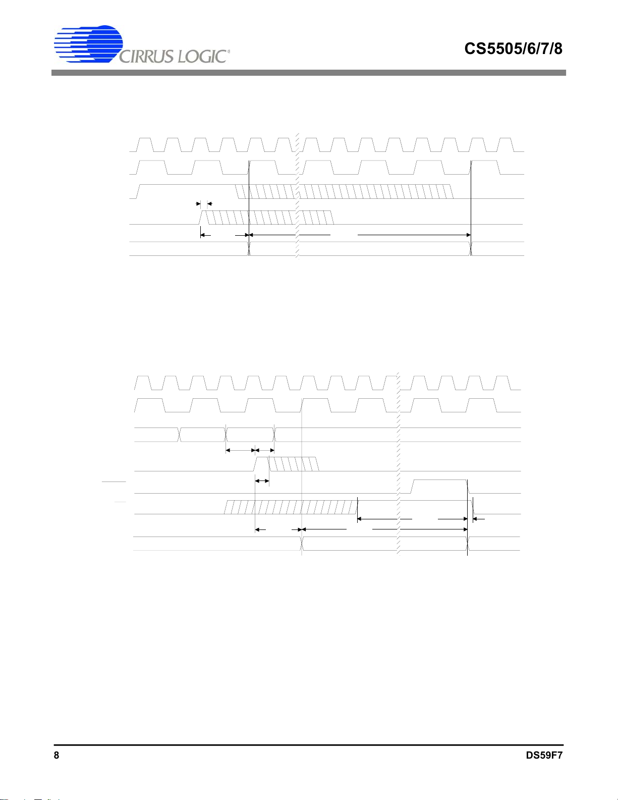
CAL
CONV
STATE
XIN
XIN/2
A0, A1
CONV
DRDY
t
ccw
t
scl
t
cal
Calibration StandbyStandby
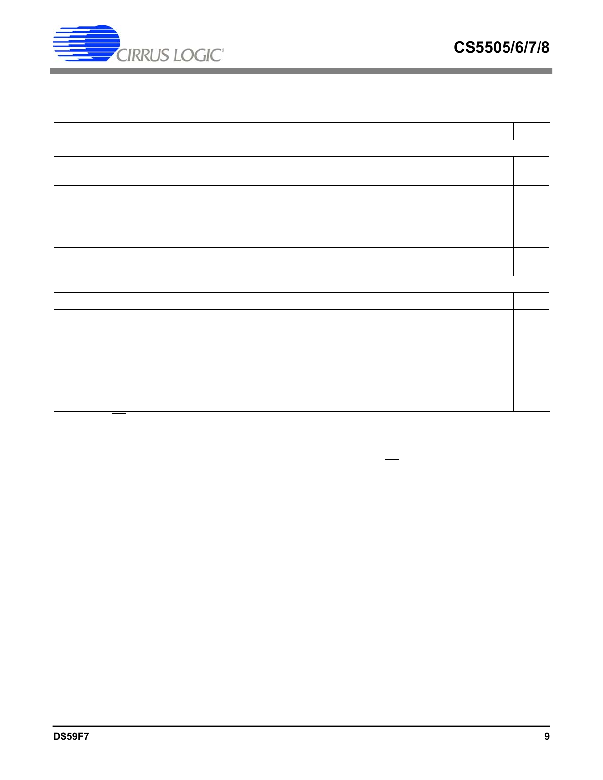
Figure 1. Calibration Timing (Not to Scale)
t
sac
t
cpw
t
hca
BP/UP
t
STATE
t
scn
t
con
Conversion StandbyStandby
bus
t
buh
Figure 2. Conversion Timing (Not to Scale)
8 DS59F4
Page 9
CS5505/6/7/8
DS59F7 9
CS5505/6/7/8
5V SWITCHING CHARACTERISTICS
(TA = T
MIN
VA- = -5V ± 10%; Input Levels: Logic 0 = 0V, Logic 1 = VD+; C
Parameter Symbol Min Typ Max Units
SSC Mode (M/SLP = VD+)
Access Time: CS Low to SDATA out (DRDY = low)
DRDY falling to MSB (CS = low)
SDATA Delay Time: SCLK falling to next SDATA bit t
SCLK Delay Time SDATA MSB bit to SCLK rising t
Serial Clock (Out) Pulse Width High
Pulse Width Low
Output Float Delay: CS high to output Hi-Z (Note 16)
SCLK rising to SDATA Hi-Z
SEC Mode (M/SLP = DGND)
Serial Clock (In) f
Serial Clock (In) Pulse Width High
Pulse Width Low
Access Time: CS Low to data valid (Note 17) t
Maximum Delay time: (Note 18)
SCLK falling to new SDATA bit t
Output Float Delay: CS high to output Hi-Z (Note 16)
SCLK falling to SDATA Hi-Z
Notes: 16. If
CS is returned high before all data bits are output, the SDATA and SCLK outputs will complete the
current data bit and then go to high impedance.
CS is activated asynchronously to DRDY, CS will not be recognized if it occ urs when DRDY is high
17. If
for 2 clock cycles. The propagation delay time may be as great as 2 f
guarantee proper clocking of SDATA when using asynchronous
sooner than 2 f
+ 200 ns after
clk
CS goes low.
18. SDATA transitions on the falling edge of SCLK. Note that a rising SCLK must occur to enable the
serial port shifting mechanism before falling edges can be recognized.
to T
= 50 pF.) (Note 2)
L
t
csd1
t
dfd
dd1
cd1
t
ph1
t
pl1
t
fd1
t
fd2
sclk
t
ph2
t
pl2
csd2
dd2
t
fd3
t
fd4
VA+, VD+ = 5V ± 10%;
MAX;
-
-
- 80 250 ns
-1/f
-
-
-
-
0-2.5MHz
200
200
- 60 200 ns
- 150 310 ns
-
-
CS, SCLK(i) should not be taken high
-
2/f
clk
clk
1/f
clk
1/f
clk
-
1/f
clk
-
-
60
160
cycles plus 200 ns. T o
clk
2/fclk
3/f
clk
-ns
-
-
2/f
clk
-
-
-
150
300
ns
ns
ns
ns
ns
ns
ns
ns
ns
ns
DS59F7 9
Page 10
CS5505/6/7/8
10 DS59F7
CS5505/6/7/8
3.3V SWITCHING CHARACTERISTICS
(TA = T
MIN
to T
5%; VA- = -5V ± 10%; Input Levels: Logic 0 = 0V, Logic 1 = VD+; C
Parameter Symbol Min Typ Max Units
SSC Mode (M/SLP = VD+)
Access Time: CS Low to SDATA out (DRDY = low)
DRDY falling to MSB (CS = low)
SDATA Delay Time: SCLK falling to next SDATA bit t
SCLK Delay Time SDATA MSB bit to SCLK rising t
Serial Clock (Out) Pulse Width High
Pulse Width Low
Output Float Delay: CS high to output Hi-Z (Note 16)
SCLK rising to SDATA Hi-Z
t
csd1
t
dfd
dd1
cd1
t
ph1
t
pl1
t
fd1
t
fd2
SEC Mode (M/SLP = DGND)
Serial Clock (In) f
Serial Clock (In) Pulse Width High
Pulse Width Low
Access Time: CS Low to data valid (Note 17) t
sclk
t
ph2
t
pl2
csd2
Maximum Delay time: (Note 18)
SCLK falling to new SDATA bit t
Output Float Delay: CS high to output Hi-Z (Note 16)
SCLK falling to SDATA Hi-Z
dd2
t
fd3
t
fd4
VA+ = 5V ± 10%; VD+ = 3.3V
MAX
= 50 pF.) (Note 2)
L
-
-
2/f
-
clk
- 265 400 ns
-1/f
-
-
-
-
1/f
1/f
1/f
clk
clk
clk
-
clk
0 - 1.25 MHz
200
200
-
-
- 100 200 ns
- 400 600 ns
-
-
70
320
±
2/fclk
3/f
clk
ns
ns
-ns
2/f
150
500
-
-
clk
-
-
-
ns
ns
ns
ns
ns
ns
ns
ns
10 DS59F4
Page 11
XIN
CS5505/6/7/8
DS59F7 11
XIN/2
CONV
CS
t
csd1
CS5505/6/7/8
STATE
DRDY
SCLK(o)
SDATA(o)
Hi-Z
Hi-Z
STATE (CONV held high)
DRDY
CS
SDATA(o) Hi-Z
SCLK(i)
StandbyStandby Conversion Conversion
t
ph1
t
pl1
Conversion1
t
cd1
MSB MSB-1
Conversion2
t
dd1
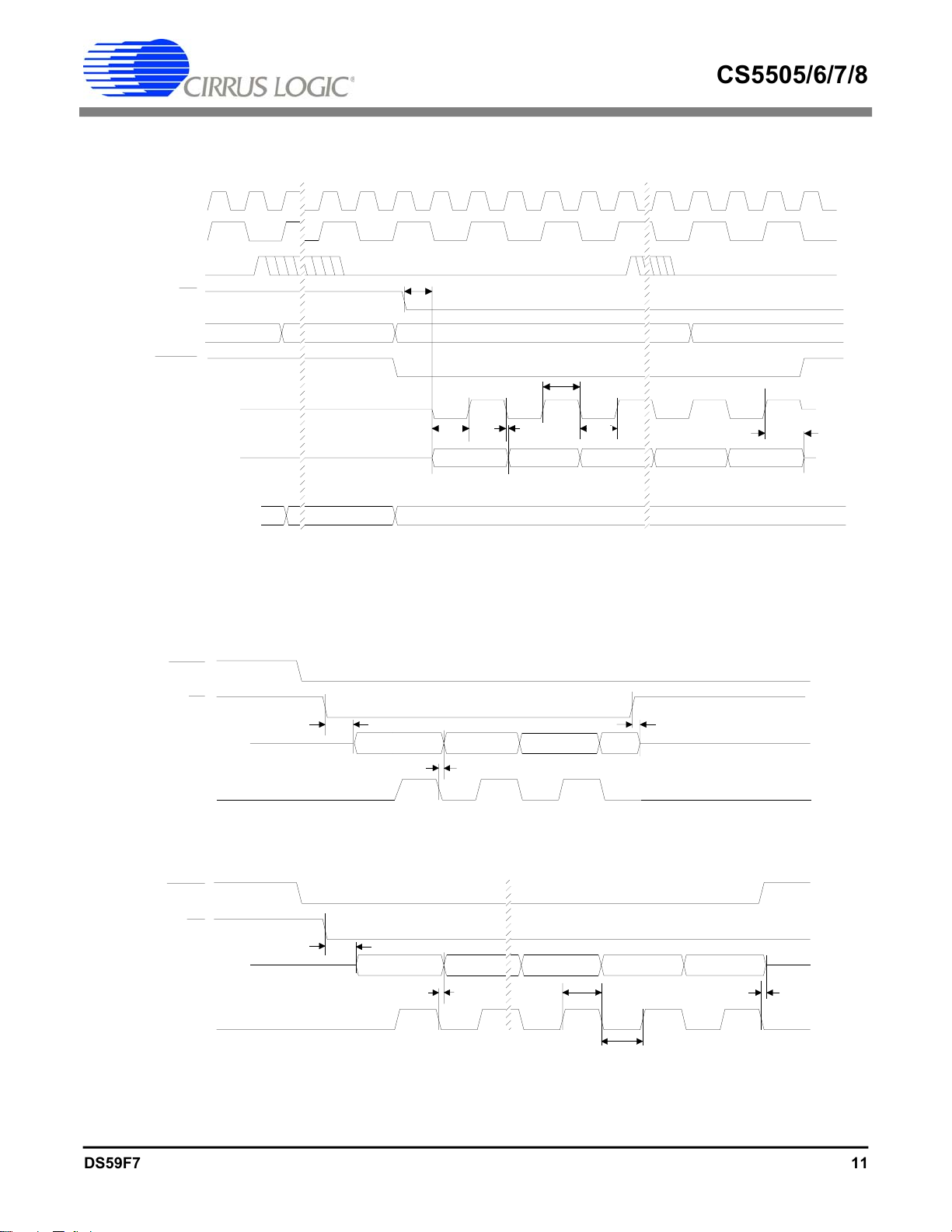
Figure 3. Timing Relationships; SSC Mode (Not to Scale)
t
csd2
t
dd2
MSB-1MSB MSB-2
t
fd2
LSB+1 LSB
t
fd3
Hi-Z
Hi-Z
DRDY
CS
t
SDATA(o) Hi-Z
SCLK(i)
csd2
t
dd2
MSB-1MSB LSB+2 LSB+1 LSB
t
ph2
t
pl2
t
fd4
Figure 4. Timing Rela tionships; SEC Mode ( Not to Scale)
DS59F4 11
Page 12

CS5505/6/7/8
12 DS59F7
RECOMMENDED OPERATING CONDITIONS (DGND = 0V) (Note 19)
Parameter Symbol Min Typ Max Units
CS5505/6/7/8
DC Power Supplies: Positive Digital
(VA+)-(VA-)
Positive Analog
Negative Analog
Analog Reference Voltage (Note 20) (VREF+)-(VREF-) 1.0 2.5 3.6 V
Analog Input Voltage: (Note 21)
Unipolar
Bipolar
Notes: 19. All voltages with r espect to ground.
20. The CS5505/6/7/8 can be operated with a reference voltage as low as 100 mV; but with a
corresponding reduction in nois e-free resolution. The common mode voltage of the voltage reference
may be any value as long as +V REF and -VREF remain inside the supply values of VA+ and VA-.
21. The CS5505/6/7/8 can acc ept input voltages up to the analog supplies (VA+ and VA-). In unipolar
mode the CS5505/6/7/8 will output all 1’s if the dc input magnitude ( (AIN+)-(AIN-)) exceeds
((VREF+)-(VREF-)) and will output all 0’s if the input becomes more negative than 0 Volts.
In bipolar mode the CS5505/6/7/8 will output all 1’s if the dc input magnitude ((AIN+)-(AIN-)) exceeds
((VREF+)-(VREF-)) and will output all 0’s if the input becomes more negative in magnitude than
-((VREF+)-(VREF-)).
VD+
V
diff
VA+
VA-
VAIN
VAIN
-((VREF+)-(VREF-))--
3.15
4.75
4.5
0
0
5.0
10
5.0
-5.0
(VREF+)-(VREF-)
+((VREF+)-(VREF-))VV
5.5
11
11
-5.5
ABSOLUTE MAXIMUM RATINGS*
Parameter Symbol Min Typ Max Units
V
V
V
V
DC Power Supplies: Digital Ground (Note 22)
Positive Digital (Note 23)
Positive Analog
Negative Analog
(VA+)-(VA-)
(VA+)-(VD+)
Input Current, Any Pin Except Supplies (Notes 24, 25) I
Analog Input Voltage AIN and VREF pins V
Digital Input Voltage V
Ambient Operating Temperature T
Storage Temperature T
Notes: 22. No pin should go more positive than (VA+)+0.3V.
23. VD+ must always be less than (VA+)+0.3 V,and can never exceed 6.0V.
24. Applies to all pins including continuous overvoltage conditions at the analog input (AIN) pin.
25. Transient currents of up to 100mA will not cause SCR latch-up. Maximum input current for a power
supply pin is ± 50 mA.
* WARNING: Operation at or beyond these limits may result in permanent damage to the device.
Normal operation is not guaranteed at these extremes.
DGND
VD+
VA+
VA-
V
diff1
V
diff2
in
INA
IND
A
stg
-0.3
-0.3
-0.3
+0.3
-0.3
-0.3
--
(VA-)-0.3 - (VA+)+0.3 V
-0.3 - (VD+)+0.3 V
-55 - 125
-65 - 150
-
-
-
-
-
-
(VD+)-0.3
6.0 or VA+
12.0
-6.0
12.0
12.0
±
10
V
V
V
V
V
V
mA
°
C
°
C
12 DS59F4
Page 13

CS5505/6/7/8
DS59F7 13
CS5505/6/7/8
GENERAL DESCRIPTION
The CS5505/6/7/8 are very low power monolithic CMOS A/D converters designed
specifically for measurement of dc signals. The
CS5505/7 are 16-bit converters (a four channel
and a single channel version). The CS5506/8 are
20-bit converters (a four channel and a single
channel version). Each of the devices includes a
delta-sigma charge-balance converter, a voltage
reference, a calibration microcontroller with
SRAM, a digital filter and a serial interface. The
CS5505 and CS5506 include a four channel
pseudo-differential (all four channels have the
same reference measurement node) multiplexer.
The CS5505/6/7/8 include an on-chip reference
but can also utilize an off-chip refere nce for precision applications. The CS5505/6/7/8 can be
used to measure either unipolar or bipolar signals. The devices use self-calibration to insure
excellent offset and gain accuracy.
The CS5505/6/7/8 are optimized to operate from
a 32.768 kHz crystal but can be driven by an
external clock whose frequency is between
30 kHz and 163 kHz. When the digital filter is
operated with a 32.768 kHz clock, the filter has
zeros precisely at 50 and 60 Hz line freque ncies
and multiple s thereof.
The CS5505/6/7/8 use a "start convert" command to latch the input channel selection and to
start a convolution cycle on the digital filter.
Once the filter cycle is completed, the output
port is updated. When operated with a
32.768 kHz clock the ADC converts and updates
its output port at 20 samples/sec. The throughput
rate per channel is the output update rate divided
by the number of channels being multiplexed. The output port includes a serial
interface with two modes of operation.
The CS5505/6/7/8 can operate from dual polarity power supplies (+5 and -5), from a single +5
volt supply, or with +10 volts on the analog and
+5 on the digital. They can also operate with
dual polarity (+5 and -5), or from a single +5
volt supply on the analog and + 3.3 on the digital.
THEORY OF OPERATION FOR THE
CS5505/6/7/8
The front page of this data sheet illustrates the
block diagram of the CS5505/6.
Basic Converter Operation
The CS5505/6/7/8 A/D converters have four operating states. These are start-up, calibration,
conversion and sleep. When power is first applied, the device enters the start-up state. The
first step is a power-on reset delay of about
10 ms which resets all of the logic in the device.
To proceed with start-up, the oscillator must
then begin oscillating. After the power-on reset
the device enters the wake-up period for 1800
clock cycles after clock is present. This allows
the delta-sigma modulator and other circuitry
(which are operating with very low currents) to
reach a stable bias condition prior to entering
into either the calibration or conversion states.
During the 1800 cycle wake-up period, the device can accept an input command. Execution of
this command will not occur until the complete
wake-up period elapses. If no command is given,
the device enters the standby mode.
Calibration
After the initial application of power, the
CS5505/6/7/8 must enter the calibration state
prior to performing accurate conversions. During
calibration, the chip executes a two-step process.
The device first performs an offset calibration
and then follows this with a gain calibration.
The two calibration steps determine the zero reference point and the full scale referenc e point of
the converter’s transfer function. From these
points it calibrates the zero point and a gain
DS59F4 13
Page 14

CS5505/6/7/8
14 DS59F7
CS5505/6/7/8
slope to be used to properly scale the output
digital codes when doing conversions.
The calibration state is entered whenever the
CAL and CONV pins are high at the same time.
The state of the CAL and CONV pins at poweron and when coming out of sleep are recognized
as commands, but will not be executed until the
end of the 1800 clock cycle wake-up period.
Note that any time CONV transitions from low
to high, the multiplexer inputs A0 and A1 are
latched internal to the CS5505 and CS5506 devices. These latched inputs select the analog
input channel which will be used once conversion commences.
If CAL and CONV become active (high) during
the 1800 clock cycle wake-up time, the converter will wait until the wake-up period elapses
before executing the calibration. If the wake-up
time has elapsed, the converter will be in the
standby mode waiting for instruction and will
enter the calibrat ion cycle immediately. The calibration lasts for 3246 clock cycles. Calibration
coefficients are then retained in the SRAM
(static RAM) for use during conversion.
At the end of the calibration cycle, the on-chip
microcontroller checks the logic state of the
CONV signal. If the CONV input is low the device will enter the standby mode where it waits
for further instruction. If the CONV signal is
high at the end of the calibration cycle, the converter will enter the conversion state and
perform a conversion on the input channel which
was selected when CONV transitioned from low
to high. The CAL signal can be returned low
any time after calibration is initiated. CONV can
also be returned low, but it should never be
taken low and then taken back high until the
calibration period has ended and the converter is
in the standby state. If CONV is taken low and
then high again with CAL high while the converter is calibrating, the device will interrupt the
current calibration cycle and start a new one. If
CAL is taken low and CONV is taken low and
then high during calibration, the calibration cycle will continue as the conversion command is
disregarded. The states of A0, A1 and BP/UP
are not important during calibrations.
If an "end of calibration" signal is desired, pulse
the CAL signal high while leaving the CONV
signal high continuously. Once the calibration is
completed, a conversion will be performed. At
the end of the conversion, DRDY will fall to indicate the first valid conversion after the
calibration has been completed.
See Understanding Converter Calibration for details on how the converter calibrates its transfer
function.
Conversion
The conversion state can be entered at the end of
the calibration cycle, or whenever the converter
is idle in the standby mode. If CONV is taken
high to initiate a calibration cycle ( CAL also
high), and remains high until the calibration cycle is compl eted (CAL is taken low after CON V
transitions high), the converter will begin a conversion upon completion of the calibration
period. The device will perform a conversion on
the input channel selected by the A0 and A1 inputs when CONV transitioned high. Table 1
indicates the multiplexer channel selection truth
table for A0 and A1.
A1 A0 Channel addressed
00 AIN1
01 AIN2
10 AIN3
11 AIN4
Table 1. Multiplexer Truth Table
The A0 and A1 inputs are latched internal to the
4-channel devices (CS5505/6) when CONV
rises. A0 and A1 have internal pull-down circuits which default the multiplexer to channel
14 DS59F4
Page 15

CS5505/6/7/8
DS59F7 15
CS5505/6/7/8
AIN1. The BP/UP pin is not a latched input. The
BP/UP pin controls how the output word from
the digital filter is processed. In bipolar mode
the output word computed by the digital filter is
offset by 8000H in the 16-bit CS5505/7 or
80000H in 20-bit CS5506/8 (see Understanding
Converter Calibration). BP/UP can be changed
after a conversion is started as long as it is stable
for 82 clock cycles of the conversion period
prior to DRDY falling. If one wishes to intermix
measurement of bipolar and unipolar signals on
various input channels, it is best to switch the
BP/UP pin immediately after DRDY falls and
leave BP/UP stable until DRDY falls again. If
the converter is beginning a conversion starting
from the standby state, BP/
UP can be changed at
the same time as A0 and A1.
The digital filter in the CS5505/6/7/8 has a Finite Impulse Response and is designed to settle
to full accuracy in one conversion time. Therefore, the multiplexer can be changed at the
conversion rate.
If CONV is left high, the CS5505/6/7/8 will perform continuous conversions on one channel.
The conversion time will be 1622 clock cycles.
If conversion is initiated from the standby state,
there may be up to two XIN clock cycles of uncertainty as to when conversion actually begins.
This is because the internal logic operates at one
half the external clock rate and the exact phase
of the internal clock may be 180° out of phase
relative to the XIN clock. When a new conversion is initiated from the standby state, it will
take up to two XIN clock cycles to begin. Actual
conversion will use 1624 clock cycles before
DRDY goes low to indicate that the serial port
has been updated. See the Serial Interface Logic
section of the data sheet for information on reading data from the serial port.
In the event the A/D conversion command
(CONV going positive) is issued during the conversion state, the current conversion will be
terminated and a new conversion will be initiated.
Voltage Reference
The CS5505/6/7/8 uses a differential voltage reference input. The positive input is VREF+ and
the negative input is VREF-. The voltage between VREF+ and VREF- can range from 1 volt
minimum to 3.6 volts maximum. The gain slope
will track changes in the reference without recalibration, accommodating ratiometric
applications.
The CS5505/6/7/8 include an on-chip voltage
reference which outputs 2.5 volts on the VREFOUT pin. This voltage is referenced to the
VA+ pin and will track changes relative to VA+.
The VREFOUT output requires a 0.1 µF capacitor connected between VREFOUT and VA+ for
stability. When using the internal reference, the
VREFOUT signal should be connected to the
VREF- input and the VREF+ pin should be connected to the VA+ supply. The internal voltage
reference is capable of sourcing 3 µA maximum
and sinking 50 µA maximum. If a more precise
reference voltage is required, an external voltage
reference should be used. If an external voltage
reference is used, the VREFOUT pin of the internal reference should be connected directly to
VA-. It cannot be left open unless the 0.1 µF capacitor is in place for stability.
CS5505/6/7/8
+VA
LT1019,
REF43
or
LM368
-VA
Figure 5. External Reference Connections
2.5V
VA+
VREF+
VREFVREFOUT
VA-
DS59F7 15
Page 16

CS5505/6/7/8
16 DS59F7
CS5505/6/7/8
CS5505/6/7/8
+VA
0.1 µF
-VA
Figure 6. Internal Reference Connections
VA+
VREF+
VREF-
VREFOUT
VA-
External reference voltages can range from 1.0
volt minimum to 3.6 volts maximum. The common mode voltage range of the external
reference can allow the reference to lie at any
voltage between the VA+ and VA- supply rails.
Figures 5 and 6 illustrate how the CS5505/6/7/8
converters are connected for external and for internal voltage reference use, respectively.
Analog Input Range
The analog input range is set by the magnitude
of the voltage between the VREF+ and VREFpins. In unipolar mode the input range will equal
the magnitude of the voltage reference. In bipolar mode the input voltage range will equate to
plus and minus the magnitude of the voltage reference. While the voltage reference can be as
great as 3.6 volts, its common mode voltage can
be any value as long as the reference inputs
VREF+ and VREF- stay within the supply volt-
ages for the A/D. The differential input voltage
can also have any common mode value as long
as the maximum signal magnitude stays within
the supply voltages.
The A/D converter is intended to measure dc or
low frequency inputs. It is designed to yield accurate conversions even with noise exceeding
the input voltage range as long as the spectral
components of this noise will be filtered out by
the digital filter. For example, with a 3.0 volt
reference in unipolar mode, the converter will
accurately convert an input dc signal up to
3.0 volts with up to 15% overrange for 60 Hz
noise. A 3.0 volt dc signal could have a 60 Hz
component which is 0.5 volts above the maximum input of 3.0 (3.5 volts peak; 3.0 volts dc
plus 0.5 volts peak noise) and still accurately
convert the input signal (XIN = 32.768 kHz).
This assumes that the signal plus noise amplitude stays within the supply voltages.
The CS5505/6/7/8 converters output data in binary format when converting unipolar signals
and in offset binary format when converting bipolar signals. Table 2 outlines the output coding
for the 16-bit CS5505/7 and the 20-bit CS5506/8
in both unipolar and bipolar measurement
modes.
CS5505 and CS5507 (16 Bit) CS5506 and CS5508 (20 Bit)
Unipolar Input
Voltage
>(VREF - 1.5 LSB) FFFF >(VREF - 1.5 LSB) >(VREF - 1.5 LSB) FFFFF >(VREF - 1.5 LSB)
VREF - 1.5 LSB FFFF
VREF/2 - 0.5 LSB 8000
+0.5 LSB 0001
<(+0.5 LSB) 0000 <(-VREF + 0.5 LSB) <(+0.5 LSB) 00000 <(-VREF + 0.5 LSB)
Note: VREF = (VREF+) - (VREF-); Table excludes common mode voltage on the signal and reference inputs.
16 DS59F7
Output
Codes
FFFE
7FFF
0000
Bipolar Input
Voltage
VREF - 1.5 LSB VREF - 1.5 LSB FFFFF
-0.5 LSB VREF/2 - 0.5 LSB 80000
-VREF + 0.5 LSB +0.5 LSB 00001
Table 2. Output Coding
Unipolar Input
Voltage
Output
Codes
FFFFE
7FFFF
00000
Bipolar Input
Voltage
VREF - 1.5 LSB
-0.5 LSB
-VREF + 0.5 LSB
Page 17

CS5505/6/7/8
DS59F7 17
CS5505/6/7/8
Understanding Converter Calibration
Calibration can be performed at any time. A
calibration sequence will minimize offset errors
and set the gain slope scale factor. The deltasigma modulator in the converter is a differential
modulator. To calibrate out offset error, the
converter internally connects the modulator differential inputs to an internal VREF- voltage and
measures the 1’s density output from the modulator. It stores the digital code representation for
this 1’s density in SRAM and remembers this
code as being the zero scale point for the A/D
conversion. The converter then connects the
negative modulator differential input to the
VREF- input and the positive modulator differential input to the VREF+ voltage. The 1’s
density output from the modulator is then recorded. The converter uses the digital
representation of this 1’s density along with the
digital code for the zero scale point and calculates a gain scale factor. The ga in scale factor is
stored in SRAM and used for calculating the
proper output codes during conversions.
The states of A0, A1 and BP/UP are ignored
during calibration but should remain stable
throughout the calibration period to minimize
noise.
When conversions are performed in unipolar
mode or in bipolar mode, the converter uses the
same calibration factors to compute the digital
output code. The only difference is that in bipolar mode the on-chip microcontroller offsets the
computed output word by a code value of
8000H (16-bit) or 80000H (20-bit) and multiplies the LSB size by two. This means that the
bipolar measurement range is not calibrated from
full scale positive to full scale negative. Instead
it is calibrated from the bipolar zero scale point
to full scale positive. The slope factor is then
extended below bipolar zero to accommodate the
negative input signals. The converter can be
used to convert both unipolar and bipolar signals
by changing the BP/UP pin. Recalibration is not
required when switching between unipolar and
bipolar modes.
Converter Performance
The CS5505/6/7/8 A/D converters have excellent
linearity performance. Calibration minimizes the
errors in offset and gain. The CS5505/7 devices
have no missing code performance to 16-bits.
The CS5506/8 devices have no missing code
performance to 20-bits. Figure 7 illustrates the
DNL of the 16-bit CS5505. The converters
achieve Common Mode Rejection (CMR) at dc
of 105 dB typical, and CMR at 50 and 60 Hz of
120 dB typical.
The CS5505/6/7/8 can experience some drift as
temperature changes. The CS5505/6/7/8 use
chopper-stabilized techniques to minimize drift.
Measurement errors due to offset or gain drift
can be eliminated at any time by recalibrating
the converter.
+1
+1/2
0
DNL (LSB)
-1/2
-1
0 65,535
Figure 7. CS5505 Differential Nonlinearity plot.
DS59F4 17
32,768
Codes
Page 18

CS5505/6/7/8
18 DS59F7
CS5505/6/7/8
Analog Input Impedance Considerations
The analog input of the CS5505/6/7/8 can be
modeled as illustrated in Figure 8 (the model ignores the multiplexer switch resistance).
Capacitors (15 pF each) are used to dynamically
sample each of the inputs (AIN+ and AIN-).
Every half XIN cycle the switch alternately connects the capacitor to the output of the buffer
and then directly to the AIN pin. Whenever the
sample capacitor is switched from the output of
the buffer to the AIN pin, a small packet of
charge (a dynamic demand of current) is required from the input source to settle the voltage
of the sample capacitor to its final value. The
voltage on the output of the buffer may differ up
to 100 mV from the actual input voltage due to
the offset voltage of the buffer. Timing allows
one half of a XIN clock cycle for the voltage on
the sample capacitor to settle to its final value.
The equation which defines the settling time is:
−
t
⁄
Ve = V
Where Ve is the final settled value, V
max
RC
e
is the
max
maximum error voltage value of the input signal,
R is the value of the input source resistance, C is
the 15 pF sample capacitor plus the value of any
stray or additional capacitance at the input pin.
The value of t is equal to 1/(2XIN).
CS5505/6/7/8
AIN+
AIN-
V
< 100 mV
os
Vos< 100 mV
Figure 8. Analog Input Model
+
-
+
-
15 pF
Internal
Bias
Voltage
15 pF
V
occurs the instant the sample capacitor is
max
switched from the buffer output to the AIN pin.
Prior to switching, AIN has an error estimated as
being less than or equal to Ve. V
is equal to
max
the prior error (Ve) plus the additional error
from the buffer offset. The estimate for V
15pF
(
15pF + C
Where C
V
= Ve + 100mV
max
is the combination of any external
EXT
EXT
max
)
or stray capacitance.
From the settling time equation, an equation for
the maximum acceptable source resistance is derived.
EXT
−1
) ln
Ve +
V
e
15pF(100mv)
(15pF
+ C
EXT
Rs
=
max
2XIN (15p F + C
This equation assumes that the offset voltage of
the buffer is 100 mV, which is the worst case.
The value of Ve is the maximum error voltage
which is acceptable.
For a maximum error voltage (Ve) of 10 µV in
the CS5505 (1/4LSB at 16-bits) and 600 nV in
the CS5506 (1/4LSB at 20-bits), the above equation indicates that when operating from a
32.768 kHz XIN, source resistances up to
110 kΩ in the CS5505 or 84 kΩ in the CS5506
are acceptable in the absence of external capacitance (C
= 0). If higher input source
EXT
resistances are desired the master clock rate can
be reduced to yield a longer settling time.
The VREF+ and VREF- inputs have nearly the
same structure as the AIN+ and AIN- inputs.
Therefore, the discussion on analog input impedance applies to the voltage reference inputs as
well.
is:
)
18 DS59F4
Page 19

CS5505/6/7/8
DS59F7 19
CS5505/6/7/8
Digital Filter Characteristics
The digital filter in the CS5505/6/7/8 is the combination of a comb filter and a low pass filter.
The comb filter has zeros in its transfer function
which are optimally placed to reject line interference frequencies (50 and 60 Hz and their
multiples) when the CS5505/6/7/8 is clocked at
32.768 kHz. Figures 9, 10 and 11 illustrate the
magnitude and phase characteristics of the filter.
0
X1 = 32.768kHz
X2 = 163.00kHz
XIN = 32.768 kHz
120
160
795.10
993.87
200
240
1193.85
-100
Attenuation (dB)
-120
-140
-160
X1
X2
-20
-40
-60
-80
0
40
0
198.9780397.95
596.92
Frequency (Hz)
Figure 9 illustrates the filter attenuation from dc
to 260 Hz. At exactly 50, 60, 100, and 120 Hz
the filter provides over 120 dB of rejection. Table 3 indicates the filter attenuation for each of
the potential line interference frequencies when
the converter is operating with a 32.768 kHz
clock. The converter yields excellent attenuation
of these interference frequencies even if the fun-
damental line frequency should vary ±1% from
its specified frequency. The -3 dB corner frequency of the filter when operating from a
32.768 kHz clock is 17 Hz. Figure 11 illustrates
that the phase characteristics of the filter are precisely linear phase.
Frequency
(Hz)
50 125.6
60 126.7
100 145.7
120 136.0
150 118.4
180 132.9
200 102.5
240 108.4
Notch
Depth
(dB)
Frequency
(Hz)
50±1%
60±1%
100±1%
120±1%
150±1%
180±1%
200±1%
240±1%
Minimum
Attenuation
(dB)
55.5
58.4
62.2
68.4
74.9
87.9
94.0
104.4
Figure 9. F ilter Magnitude Plot to 26 0 Hz
0
-20
-40
-60
-80
Attenuation (dB)
-100
-120
-140
0 5 10 15 20 25 30 35 40 45 50
Flatness
Frequency
1
2
3
4
5
6
7
8
9
10
17
dB
-0.010
-0.041
-0.093
-0.166
-0.259
-0.374
-0.510
-0.667
-0.846
-1.047
-3.093
Frequency (Hz)
XIN = 32.768 kHz
Figure 10. Filter Magnitude Plot to 50 Hz
Table 3. Filter Notch Attenuation (XIN = 32.768 kHz)
180
135
90
45
0
-45
Phase (Degrees)
-90
XIN = 32.768 kHz
-135
-180
0 5 10 15 20 25 30 35 40 45 50
Frequency (Hz)
Figure 11. Filter Phase Plot to 50 Hz
DS59F4 19
Page 20

CS5505/6/7/8
20 DS59F7
CS5505/6/7/8
If the CS5505/6/7/8 is operated at a clock rate
other than 32.768 kHz, the filter characteristics,
including the comb filter zeros, will scale with
the operating clock frequency. Therefore, optimum rejection of line frequency interference will
occur with the CS5505/6/7/8 running at
32.768 kHz. The CS5505/6/7/8 can be used with
external clock rates from 30 kHz to 163 kHz.
Anti-Alias Con sideratio ns for Spec tral
Measurement Applications
Input frequencies greater than one half the output word rate (CONV = 1) may be aliased by
the converter. To prevent this, input signals
should be limited in frequency to no greater than
one half the output word rate of the converter
(when CONV =1). Frequencies close to the
modulator sample rate (XIN/2) and multiples
thereof may also be aliased. If the signal source
includes spectral components above one half the
output word rate (when CONV = 1) these com-
ponents should be removed by means of lowpass filtering prior to the A/D input to prevent
aliasing. Spectral components greater than one
half the output word rate on the VREF inputs
(VREF+ and VREF-) may also be aliased. Filtering of the reference voltage to remove these
spectral components from the reference voltage
is desirable.
Crystal Oscillator
The CS5505/6/7/8 is designed to be operated using a 32.768 kHz "tuning fork" type crystal. One
end of the crystal should be connected to the
XIN input. The other end should be attached to
XOUT. Short lead lengths should be used to
minimize stray capacitance. Figure 12 illustrates
the gate oscillator, and a simplified version of
the control logic used on the chip.
Over the industrial temperature range (-40 to
+85 °C) the on-chip gate oscillator will oscillate
A0
A1
CONV
CAL
CS5505/6
Channel A0 A1
1
2
3
4
S
Q
D
R
S
R
T
XIN
CLK
Q
D
CLK
Q
0
0
1
1
Start
Q
Conversion
Start
Q
Calibration
Modulator
Sample
Clock
22.5 pF
XOUT
gm
D
Q
CLK
D
Q
CLK
10 M
~
19 umho
~
Input
Mux
Decoder
R
Ω
15 pF
XTL=32.768 kHz
Figure 12. Gate Oscillator and Control Logic
0
1
0
1
20 DS59F4
Page 21

CS5505/6/7/8
DS59F7 21
CS5505/6/7/8
with other crystals in the range of 30 kHz to
53 kHz. Over the military temperature range (-
55 to +125 °C) the on-chip gate oscillator is
designed to work only with a 32.768 kHz crystal. The chip will operate with external clock
frequencies from 30 kHz to 163 kHz.over all
temperature ranges. The 32.768 kHz crystal is
normally specified as a time-keeping crystal with
tight specifications for both initial frequency and
for drift over temperature. To maintain excellent
frequency stability, these crystals are specified
only over limited operating temperature ranges
(i.e. -10 to +60 °C) by the manufacturers. Applications of these crystals with the CS5505/6/7/8
do not require tight initial tolerance or low
tempco drift. Therefore, a lower cost crystal with
looser initial tolerance and tempco will generally
be adequate for use with the CS5505/6/7/8 converters. Also check with the manufacturer about
wide temperature range application of their
standard crystals. Generally, even those crystals
specified for limited temperature range will operate over much larger ranges if frequency
stability over temperature is not a requirement.
The frequency stability can be as bad as ±3000
ppm over the operating temperature range and
still be typically better than the line frequency
(50 or 60 Hz) stability over cycle to cycle during
the course of a day. There are crystals available
for operation over the military temperature range
(-55 to +125 °C). See the Appendix for suppliers
of 32.768 kHz crystals.
Serial Interface Logic
When new data is put into the port DRDY will
go low.
Data can be read from the serial port in either of
two modes. The M/SLP pin determines which
serial mode is selected. Serial port mode selection is as follows:
SSC (Synchronous Self-Clocking) mode;
M/SLP = VD+, or SEC (Synchronous External
Clocking) mode; M/SLP = DGND. Timing diagrams which illustrate the SSC and SEC timing
are in the tables section of this data sheet.
Synchronous Self-Clocking Mode
The serial port operates in the SSC mode when
the M/SLP pin is connected to the VD+ pin on
the part. In SSC mode the CS5505/6/7/8 furnishes both the serial output data (SDATA) and
the serial clock (SCLK). When the serial port is
updated at the end of a conversion, DRDY falls.
If CS is low, the SDATA and SCLK pins will
come out of the high impedance state two XIN
clock cycles after DRDY falls. The MSB data
bit will be presented for two cycles of XIN
clock. The SCLK signal will rise in the middle
of the MSB data bit. When SCLK then returns
low the (MSB - 1) bit will appear. Subsequent
data bits will be output on each falling edge of
SCLK until the LSB data bit is output. After the
LSB data bit is output, the SCLK will fall at
which time both the SDATA and SCLK outputs
will return to the high impedance output state.
DRDY will return h igh at this time.
The digital filter in the CS5505/6/7/8 takes 1624
clock cycles to compute an output word once a
conversion begins. At the end of the conversion
cycle, the filter will attempt to update the serial
port. Two clock cycles prior to the update
DRDY will go high. When DRDY goes high
just prior to a port update it checks to see if the
port is either empty or unselected (CS = 1). If
the port is empty or unselected, the digital filter
will update the port with a new output word.
If CS is taken low after DRDY falls, the MSB
data bit will appear within two XIN clock cycles
after CS is taken low. CS need not be held low
for the entire data output. If CS is returned high
during a data bit the port will complete the output of that bit and then go into the Hi-Z state.
The port can be reselected any time prior to the
completion of the next conversion (DRDY falling) to allow the remaining data bits to be
output.
DS59F4 21
Page 22

CS5505/6/7/8
22 DS59F7
CS5505/6/7/8
Synchronous External-Clocking Mode
The serial port operates in the SEC mode when
the M/SLP pin is connected to the DGND pin.
SDATA is the output pin for the serial data.
When CS goes low after new data becomes
available (DRDY goes low), the SDATA pin
comes out of Hi-Z with the MSB data bit present. SCLK is the input pin for the serial clock
in the SEC mode. If the MSB data bit is on the
SDATA pin, the first rising edge of SCLK enables the shifting mechanism. This allows the
falling edges of SCLK to shift subsequent data
bits out of the port. Note that if the MSB data
bit is output and the SCLK signal is high, the
first falling edge of SCLK will be ignored because the shifting mechanism has not become
activated. After the first rising edge of SCLK,
each subsequent falling edge will shift out the
serial data . Once the LSB is prese nt, the falling
edge of SCLK will cause the SDATA output to
go to Hi-Z and DRDY to return high. The serial
port register will be updated with a new data
word upon the completion of another conversion
if the serial port has been emptied, or if the CS
is inactive (high).
CS can be operated asynchronously to the
DRDY signal. The DRDY signal need not be
monitored as long as the CS signal is taken low
for at least two XIN clock cycles plus 200 ns
prior to SCLK being toggled. This ensures that
CS has gained control over the serial port.
Sleep Mode
The CS5505/6/7/8 devices offer two methods of
putting the device into a SLEEP condition to
conserve power. Calibration words will be retained in SRAM during either sleep condition.
The M/SLP pin can be put into the SLEEP
threshold to lower the operating power used by
the device to about 1% of nominal. Alternately,
the clock into the XIN pin can be stopped. This
will lower the power consumed by the converter
to about 30% of nominal. In both cases, the
converter must go through a wake-up sequence
prior to conversions being initiated. This wakeup sequence includes the 10 msec. (typ.)
power-on-reset delay, the start-up of the oscillator (unless an external clock is used), and the
1800 clock cycle wake-up delay after the clock
begins. When coming out of the sleep condition, the converter will latch the A0 and A1
inputs.
Figure 13 illustrates how to use a gate and resistors to bias the M/SLP pin into the SLEEP
threshold region when using the converter in the
SSC mode. To use the SEC mode return resistor
R1 to DGND instead of the supply. When in
the SEC mode configuration the CS5505/6/7/8
will enter the SLEEP threshold when the logic
control input is a logic 1 (VD+). Note that large
resistors can be used to conserve power while in
sleep. The input leakage of the pin is typically
less than 1 µA even at 125 °C, although the
worst case specification tables indicate a leakage
*
VD+
**
1%
R
Control
Input
’1’ = SSC Mode
’0’ = SLEEP
*
Tie R to DGND for SEC mode; control input
1
logic inverts.
**
R = 499k, V + = 5V; R = 590k, V + = 3.3V
1 1
Figure 13. Sleep Threshold Control
2
499k
1%
DD
R
1
0.01µF
CS5505/6/7/8
M/SLP
of 10 µA maximum.
Power Supplies and Grounding
The analog and digital supply pins to the
CS5505/6/7/8 are brought out on separate pins to
minimize noise coupling between the analog and
digital sections of the chip. Note that there is no
22 DS59F7
Page 23

CS5505/6/7/8
DS59F7 23
CS5505/6/7/8
analog ground pin. No analog ground pin is required because the inputs for measurement and
for the voltage reference are differential and require no ground. In the digital section of the
chip the supply current flows into the VD+ pin
and out of the DGND pin. As a CMOS device,
the CS5505/6/7/8 requires that the supply voltage on the VA+ pin always be more positive
than the voltage on any other pin of the device.
If this requirement is not met, the device can
latch-up or be damaged. In all circumstances the
VA+ voltage must remain more positive than the
+5V
Analog
Supply
Calibration
Control
0.1
µ
F
4
CAL
VD+ or DGND pins; VD+ must remain more
positive than the DGND pin.
The following power supply options are possible:
VA+ = +5V to +10V, VA- = 0V, VD+ = +5V
VA+ = +5V, VA- = -5V, VD+ = +5V
VA+ = +5V , VA- = 0V to -5V, VD+ = +3.3V
The CS5505/6/7/8 cannot be operated with a
3.3V digital supply if VA+ is greater than
+5.5V.
10
Ω
0.1
µ
F
17
VA+
20
VD+
XIN
XOUT
5
6
Optional
Clock
Source
32.768 kHz
Analog*
Signal
Sources
Signal
Ground
Voltage
Reference
Note:
Bipolar/
Unipolar
Input Select
*Unused analog inputs
should be tied to AIN-
+
-
To use the internal 2.5 volt reference see Figure 6.
8
9
10
12
13
11
14
15
16
BP/UP
CS5505/6
AIN1+
AIN2+
AIN3+
AIN4+
AIN-
VREF+
VREF-
VREFOUT
VA-
18
M/SLP
SCLK
SDATA
DRDY
CS
A0
A1
CONV
DGND
7
21
22
23
2
1
24
3
19
Sleep Mode
Control
and
Output Mode
Select
Serial
Data
Interface
Control
Logic
Unused Logic
inputs must be
connected to
VD+ or DGND.
Figure 14. CS5505/6 System Connection Diagram Us ing External Reference, Single Supply
DS59F7 23
Page 24

CS5505/6/7/8
24 DS59F7
CS5505/6/7/8
Figure 14 illustrates the System Connection Dia-
gram for the CS5505/6 using a single +5V
supply. Note that all supply pins are bypassed
with 0.1 µF capacitors and that the VD+ digital
supply is derived from the VA+ supply.
Figure 15 illustrates the CS5505/6 using dual
supplies of +5 and -5V.
+5V
Analog
Supply
Analog*
Signal
Sources
Signal
Ground
Voltage
Reference
-5V
Analog
Supply
Calibration
Control
Bipolar/
Unipolar
Input Select
*Unused analog inputs
should be tied to AIN-
+
-
0.1
0.1
µ
µ
F
4
CAL
8
BP/UP
9
AIN1+
10
AIN2+
12
AIN3+
13
AIN4+
11
AIN-
14
VREF+
15
VREF-
16
VREFOUT
F
Figure 16 illustrates the CS5505/6 using dual
supplies of +10V analog and +5V digital.
When using separate supplies for VA+ and
VD+, VA+ must be established first. VD+
should never become more positive than VA+
under any operating condition. Remember to investigate transient power-up conditions, when
one power supply may have a faster rise time.
Ω
10
0.1
µ
F
17
VA+
CS5505/6
VA-
18
20
VD+
XIN
XOUT
M/SLP
SCLK
SDATA
DRDY
CS
A0
A1
CONV
DGND
5
6
7
21
22
23
2
1
24
3
19
Optional
Clock
Source
32.768 kHz
Sleep Mode
Control
and
Output Mode
Select
Serial
Data
Interface
Control
Logic
Unused Logic
inputs must be
connected to
VD+ or DGND.
Note:
24 DS59F7
To use the internal 2.5 volt reference see Figure 6.
Figure 15. CS5505/6 System Connection Diagram Using External Reference, Dual Supplies
Page 25

CS5505/6/7/8
DS59F7 25
CS5505/6/7/8
+10V
Analog
Supply
Analog*
Signal
Sources
Signal
Ground
Voltage
Reference
0.1
µ
F
Calibration
Control
Bipolar/
Unipolar
Input Select
*Unused analog inputs
should be tied to AIN-
+
(1)
-
4
8
9
10
12
13
11
14
15
16
17
CAL
BP/UP
CS5505/6
AIN1+
AIN2+
AIN3+
AIN4+
AIN-
VREF+
VREF-
VREFOUT
VA-
18
(2)
20
VD+VA+
XIN
XOUT
M/SLP
SCLK
SDATA
DRDY
CS
A0
A1
CONV
DGND
0.1
µ
5
6
32.768 kHz
7
21
22
23
2
1
24
3
19
F
Analog
Supply
Optional
Clock
Source
Sleep Mode
Control
and
Output Mode
Select
Serial
Data
Interface
Control
Logic
Unused Logic
inputs must be
connected to
VD+ or DGND.
+5V
Note:
(1) To use the internal 2.5 volt reference see Figure 6.
(2) VD+ must never exceed VA+. Examine power-up conditions.
Figure 16. CS5505/6 System Connection Diagram Using External Reference,
Dual Supply, +10V Analog, +5V Dig ital
Schematic & Layout Review Service
Confirm Optimum
Confirm Optimum
Schematic & Layout
Schematic & Layout
Before Building Your Board.
Before Building Your Board.
For Our Free Review Service
For Our Free Review Service
Call Applications Engineering.
Call Applications Engineering.
Call: (512) 445-7222
DS59F4 25
Page 26

PIN CONNECTIONS*
CS5505/6/7/8
26 DS59F7
CS5505/6
CS5505/6/7/8
MULTIPLEXER SELECTION INPUT A0 A1 MULTIPLEXER SELECTION INPUT
CHIP SELECT
CONVERT CONV SDATA SERIAL DATA OUTPUT
CALIBRATE CAL SCLK SERIAL CLOCK INPUT/OUTPUT
CRYSTAL IN XIN VD+ POSITIVE DIGITAL POWER
CRYSTAL OUT XOUT DGND DIGITAL GROUND
SE RIAL MODE/ SLEEP M/SLP VA- NEGATIVE ANALOG POWER
BIPOLAR/UNIPOLAR BP/
DIFFERENTIAL ANALOG INPUT AIN1+ VREFOUT VOLTAGE REFERENCE OUTPUT
DIFFERENTIAL ANALOG INPUT AIN2+ VREF- VOLTAGE REFERENCE INPUT
DIFFERENTIAL ANALOG RETURN AIN- VREF+ VOLTAGE REFERENCE INPUT
DIFFERENTIAL ANALOG INPUT AIN3+ AIN4+ DIFFERENTIAL ANALOG INPUT
CHIP SELECT
CS DRDY DATA READY
CONVERT CONV SDATA SERIAL DATA OUTPUT
CALIBRATE CAL SCLK SERIAL CLOCK INPUT/OUTPUT
CRYSTAL IN XIN VD+ POSITIVE DIGITAL POWER
CRYSTAL OUT XOUT DGND DIGITAL GROUND
SERIAL MODE/ SLEEP M/SLP VA- NEGATIVE ANALOG POWER
BIPOLAR/UNIPOLAR BP/
UP VA+ POSITIVE ANALOG POWER
DIFFERENTIAL ANALOG INPUT AIN+ VREFOUT VOLTAGE REFERENCE OUTPUT
NO CONNECTION NC VREF- VOLTAGE REFERENCE INPUT
DIFFERENTIAL ANALOG INPUT AIN- VREF+ VOLTAGE REFERENCE INPUT
1
CS DRDY DATA READY
2
3
4
5
6
7
UP VA+ POSITIVE ANALOG POWER
8
9
10
11
12
CS5507/8
1
2
3
4
5
6
7
8
9
10
24
23
22
21
20
19
18
17
16
15
14
13
20
19
18
17
16
15
14
13
12
11
*Pinout applies to both DIP and SOIC
26 DS59F4
Page 27

PIN DESCRIPTIONS
CS5505/6/7/8
DS59F7 27
Pin numbers for four channel devices are in parentheses.
Clock Generator
XIN; XOUT - Crystal In; Crystal Out, Pins 4 (5) and 5 (6).
A gate inside the chip is connected to these pins and can be used with a crystal to provide the
master clock for the device. Alternatively, an external (CMOS compatible) clock can be
supplied into the XIN pin to provide the master clock for the device. Loss of clock will put the
device into a lower powered state (approximately 70% power reduction).
Serial Output I/O
M/SLP - Serial Interfac e Mode Sele ct/ Sleep, Pin 6 (7).
Dual function pin which selects the operating mode of the serial port and provides a very low
power sleep function. When M/SLP is tied to the VD+ pin the serial port will operate in the
Synchronous Self-Clocking (SSC) mode. When M/SLP is tied to the DGND pin the serial port
will operate in the Synchronous External Clocking (SEC) mode. When the M/SLP pin is tied
half way between VD+ and DGND the chip will enter into a very low powered sleep mode in
which its calibration data will be maintained.
CS5505/6/7/8
CS - Chip Select, Pin 1 (2).
This input allows an external device to access the serial port.
DRDY - Data Ready, Pin 20 (23)
Data Ready goes low at the end of a digital filter convolution cycle to indicate that a new
output word has been placed into the serial port. DRDY will return high after all data bits are
shifted out of the serial port or two master clock cycles before new data becomes available if
the CS pin is inactive (high).
SDATA - Serial Data Output, Pin 19 (22).
SDATA is the output pin of the serial output port. Data from this pin will be output at a rate
determined by SCLK and in a format determined by the M/SLP pin. Data is output MSB first
and advances to the next data bit on the falling edges of SCLK. SDATA will be in a high
impedance state when not transmitting data.
SCLK - Serial Clock Input/Output, Pin 18 (21).
A clock signal on this pin determines the output rate of the data from the SDATA pin. The
M/SLP pin determines whether SCLK is an input or and output. When used as an input, it must
not be allowed to float.
DS59F7 27
Page 28

Control Input Pins
CS5505/6/7/8
28 DS59F7
CAL - Calibrate, Pin 3 (4).
When taken high the same time that the CONV pin is taken high the c onverter will perform a
self-calibration which includes calibration of the offset and gain scale factors in the converter.
CONV - Convert, Pin 2 (3).
The CONV pin initiates a calibration cycle if it is taken from low to high while the CAL pin is
high, or it initiates a conversion if it is taken from low to high with the CAL pin low. CONV
latches the multiplexer selection when it transitions from low to high on the multiple channel
devices. If CONV is held high (CAL low) the converter will do continuous conversions.
A0, A1 - Multiplexer Selection Inputs, Pins (1, 24).
A0 and A1 select the input channel for conversion on the multi-channel input devices. A0 and
A1 are latched when CONV transitions from low to high. These two inputs have pull-down
resistors internal to the chip.
BP/UP - Bipolar/Unipolar, Pin 7 (8).
The BP/UP pin selects the conversion mode of the converter. When high the converter will
convert bipolar input signals; when low it will convert unipolar input signals.
CS5505/6/7/8
Measurement and Reference Inputs
AIN+, AIN-, (AIN1+, AIN2+, AIN3+, AIN4+, AIN-) - Differential Analog Inputs, Pins 8, 10 (9,
10, 12, 13, 11).
AIN- in the CS5505/6 is a common measurement node for AIN1+, AIN2+, AIN3+ and AIN4+.
VREF+, VREF- - Differential Voltage Reference Inputs, Pins 11, 12 (14, 15).
A differential voltage reference on these pins operates as the voltage reference for the
converter. The voltage between these pins can be any voltage between 1.0 and 3.6 volts.
Voltage Reference
VREFOUT - Voltage Reference Output, Pin 13 (16).
The on-chip voltage reference is output from this pin. The voltage reference has a nominal
magnitude of 2.5 volts and is referenced to the VA+ pin on the converter.
Power Supply Connections
VA+ - Positive Analog Power, Pin 14 (17).
Positive analog supply voltage. Nominally +5 volts.
VA- - Negative Analog Power, Pin 15 (18).
Negative analog supply voltage. Nominally -5 volts when using dual polarity supplies; or 0
volts (tied to system analog ground) when using single supply operation.
28 DS59F4
Page 29

VD+ - Positive Digital Power, Pin 17 (20).
CS5505/6/7/8
DS59F7 29
Positive digital supply voltage. Nominally +5 volts or 3.3 volts.
DGND - Digital Ground, Pin 16 (19).
Digital Ground.
Other
NC - No Connection, Pin 9.
Pin should be left floating.
SPECIFICATION DEFINITIONS
Linearity Error
The deviation of a code from a straight line which connects the two endpoints of the A/D
Converter transfer function. One endpoint is located 1/2 LSB below the first code transition
and the other endpoint is located 1/2 LSB beyond the code transition to all ones. Units in
percent of full-scale.
CS5505/6/7/8
Differential Nonlinearity
The deviation of a code’s width from the ideal width. Units in LSBs.
Full Scale Error
The deviation of the last code transition from the ideal [{(VREF+) - (VREF-)} - 3⁄2 LSB].
Units are in LSBs.
Unipolar Offset
The deviation of the first code transition from the ideal (1⁄2 LSB above the voltage on the AINpin.) when in unipolar mode (BP/UP low). Units are in LSBs.
Bipolar Offset
The deviation of the mid-scale transition (011...111 to 100...000) from the ideal (1⁄2 LSB below
the voltage on the AIN- pin.) when in bipolar mode (BP/UP high). Units are in LSBs
DS59F7 29
Page 30

ORDERING INFORMATION
Model Resolution
CS5505/6/7/8
Liearity
Error Channels Package Temperature
CS5505-ASZ (lead free) 16 Bits 0.0030%
4 24-pin SOIC
CS5506-BSZ (lead free) 20 Bits 0.0015%
CS5507-ASZ (lead free) 16 Bits 0.0030%
1 20-pin SOIC
CS5508-BSZ (lead free) 20 Bits 0.0015%
ENVIRONMENTAL, MANUFACTURING, & HANDLING INFORMATION
Model Number Peak Reflow Temp MSL Rating* Max Floor Life
CS5505-ASZ (lead free)
CS5506-BSZ (lead free)
260 °C 3 7 Days
CS5507-ASZ (lead free)
CS5508-BSZ (lead free)
* MSL (Moisture Sensitivity Level) as specified by IPC/JEDEC J-STD-020.
-40 to +85 °C
30 DS59F7
Page 31

REVISION HISTORY
Contacting Cirrus Logic Support
For all product questions and inquiries contact a Cirrus Logic Sales Representative.
To find the one nearest to you go to www.cirrus.com
IMPORTANT NOTICE
Cirrus Logic, Inc. and its subsidiaries (“Cirrus”) believe that the information contained in this document is accurate and reliable. However, the information is subject
to change without notice and is provided “AS IS” without warranty of any kind (express or implied). Customers are advised to obtain the latest version of relevant
information to verify, before placing orders, that information being relied on is current and complete. All products are sold subject to the terms and conditions of sale
supplied at the time of order acknowledgment, including those pertaining to warranty, indemnification, and limitation of liability. No responsibility is assumed by Cirrus
for the use of this information, including use of this information as the basis for manufacture or sale of any items, or for infringement of patents or other rights of third
parties. This document is the property of Cirrus and by furnishing this information, Cirrus grants no license, express or implied under any patents, mask work rights,
copyrights, trademarks, trade secrets or other intellectual property rights. Cirrus owns the copyrights associated with the information contained herein and gives consent for copies to be made of the information only for use within your organization with respect to Cirrus integrated circuits or other products of Cirrus. This consent
does not extend to other copying such as copying for general distribution, advertising or promotional purposes, or for creating any work for resale.
CERTAIN APPLICATIONS USING SEMICONDUCTOR PRODUCTS MAY INVOLVE POTENTIAL RISKS OF DEATH, PERSONAL INJURY, OR SEVERE PROPERTY OR ENVIRONMENTAL DAMAGE (“CRITICAL APPLICATIONS”). CIRRUS PRODUCTS ARE NOT DESIGNED, AUTHORIZED OR WARRANTED FOR USE
IN PRODUCTS SURGICALLY IMPLANTED INTO THE BODY, AUTOMOTIVE SAFETY OR SECURITY DEVICES, LIFE SUPPORT PRODUCTS OR OTHER CRITICAL APPLICATIONS. INCLUSION OF CIRRUS PRODUCTS IN SUCH APPLICATIONS IS UNDERSTOOD TO BE FULLY AT THE CUSTOMER'S RISK AND CIRRUS DISCLAIMS AND MAKES NO WARRANTY, EXPRESS, STATUTORY OR IMPLIED, INCLUDING THE IMPLIED WARRANTIES OF MERCHANTABILITY AND
FITNESS FOR PARTICULAR PURPOSE, WITH REGARD TO ANY CIRRUS PRODUCT THAT IS USED IN SUCH A MANNER. IF THE CUSTOMER OR CUSTOMER'S CUSTOMER USES OR PERMITS THE USE OF CIRRUS PRODUCTS IN CRITICAL APPLICATIONS, CUSTOMER AGREES, BY SUCH USE, TO FULLY
INDEMNIFY CIRRUS, ITS OFFICERS, DIRECTORS, EMPLOYEES, DISTRIBUTORS AND OTHER AGENTS FROM ANY AND ALL LIABILITY, INCLUDING ATTORNEYS' FEES AND COSTS, THAT MAY RESULT FROM OR ARISE IN CONNECTION WITH THESE USES.
Cirrus Logic, Cirrus, and the Cirrus Logic logo designs are trademarks of Cirrus Logic, Inc. All other brand and product names in this document may be trademarks
or service marks of their respective owners.
Revision Date Changes
F4 MAR 1995 First Final Release
F5 AUG 2005 Updated device ordering info. Updated legal notice. Added MSL data..
F7 OCT 2009 Increased minimum Vdiff voltage from 4.5 to 4.75 V.
CS5505/6/7/8
DS59F7 31
Page 32

- NOTES -
CS5505/6/7/8
32 DS59F7
Page 33

CDB5505/6/7/8
N
Copyright Cirrus Logic, Inc. 2009
(All Rights Reserved)
http://www.cirrus.com
CDB5505/6/7/8
Evaluation Board for CS5505/6/7/8 Series of ADCs
JUN ‘09
DS59DB4
CDB No Longer Available
For Reference Only
Evaluation Board for CS5505/6/7/8 Series of ADC’s
Features
l
Operation with on-board 32.768 kHz crystal
or off-board clock source
l
Jumper selectable:
- SSC mode; SEC mode; Sleep
l
DIP Switch Selectable:
- BP/UP mode; A0, & A1 channel selection
l
On-board precision voltage reference
l
Access to all digital control pins
l
On-board patch area
I
AIN4+
AIN3+
AIN2+
Description
The CDB5505/ 5506/5507/5508 is a ci rcuit boa rd d esigned to provide quick evaluation of the CS5505/6/7/8
series of A/D converters. The board can be configured to
evaluate the CS5505/6/7/8 in either SSC (Synchronous
Self-Clocking) or SEC (Synchronous External-Clocking)
serial port mode.
The board allows access to all of the digital interface pins
of the CS5505/6/7/8 chip.
ORDERING INFORMATION
CDB5505 Evaluation Board
CDB5506 Evaluation Board
CDB5507 Evaluation Board
CDB5508 Evaluation Board
CS5505/6/7/8
B
U
F
F
E
R
S
H
E
A
D
E
R
AIN1+
AIN-
VREF
+5V
GND
Cirrus Logic, Inc.
Crystal Semiconductor Products Division
P.O. Box 17847, Austin, Texas 78760
(512) 445 7222 FAX: (512) 445 7581
http://www.crystal.com
Copyright © Cirrus Logic, Inc. 1998
-5V
(All Rights Reserved)
CLKI
MAR ‘95
DS59DB2
33
Page 34

Introduction
CDB5505/6/7/8
34 DS59DB4
CDB No Longer Available
For Reference Only
CS5505/6/7/8
The CDB5505/6/7/8 evaluation board provides a
quick means of testing the CS5505/6/7/8 series
A/D converters. The CS5505/6/7/8 converters
require a minimal amount of external circuitry.
The evaluation board comes configured with the
A/D converter chip operating from a 32.768 kHz
crystal and with an off-chip precision 2.5 volt
reference. The board provides access to all of
the digital interface pins of the CS5505/6/7/8
chip.
The board is configured for operation from +5
and -5 volt power supplies, but can be operated
from a single +5 volt supply if the -5V binding
post is shorted to the GND binding post.
Evaluation Board Overview
The board provides a complete means of making
the CS5505/6/7/8 A/D converter chip function.
The user must provide a means of taking the
output data from the board in serial format and
using it in his system.
Figure 1 illustrates the schematic for the board.
The board comes configured for the A/D converter chip to operate from the 32.768 kHz
watch crystal. A BNC connector for an external
clock is provided on the board. To connect the
external BNC source to the converter chip, a circuit trace must be cut. Then a jumper must be
inserted in the proper holes to connect the XIN
pin of the converter to the input line from the
BNC. The BNC input is terminated with a 50Ω
resistor. Remove this resistor if driving from a
logic gate. See the schematic in Figure 1.
The board comes with the A/D converter
VREF+ and VREF- pins hard-wired to the
2.5 volt bandgap voltage reference IC on the
board. The VREF+ and VREF- pins can be connected to either the on chip reference or an
off-board reference if the connections (2A and
2B) to the bandgap IC are cut.
Note that the pin-out of the CS5505/6/7/8 series
chips allows the 20-pin single channel devices to
be plugged into the 24-pin, four channel footprint. See Figure 2 which illustrates the footprint
compatib ility.
Prior to powering up the board, select the serial
port operating mode with the appropriate jumper
on the M/SLP header. The device can be operated in either the SSC (Synchronous
Self-Clocking) or the SEC (Synchronous External Clocking) mode. See the device data sheet
for an explanation of these modes.
All of the control pins of the CS5505/6/7/8 are
available at the J1 header connector. Buffer ICs
U2 and U3 are used to buffer the converter for
interface to off-board circuits. The buffers are
used on the evaluation board only because the
exact loading and off-board circuitry is unknown. Most applications will not require the
buffer ICs for proper operation.
To put the board in operation, select either bipolar or unipolar mode with DIP switch S2. Then
press the CAL pushbutton after the board is
powered up. This initiates calibration of the converter which is required before measurements
can be taken.
To select an input channel on the four channel
devices, use DIP switch S2 to select the inputs
A1 A0 Channel addressed
00 AIN1
01 AIN2
10 AIN3
11 AIN4
Table 1. Multiplexer Truth Table
34 DS59DB2
Page 35

+5
CDB5505/6/7/8
DS59DB4 35
CDB No Longer Available
For Reference Only
+5
DRDY
SCLKI
SCLKO
SDATA
DRDY
A1
A0
CS
CONV
SCLK
SDATA
CAL
BP/UP
CS5505/6/7/8
R22
+5
J2
F
µ
C16
10
+
U2F
13
F
µ
R1
C18
0.1
2
U3A
VD+
14
6
4
U3B
5
8
VD+
100k
R24
R25
100k
TP13
21
SCLK
AIN3+
AIN4+
12
10
TP4
TP5
R6
R7
402
402
100k
R28
R29
100k
AIN4+
AIN3+
10
R11
100k
R10 20k
F
CAL
µ
C11
0.01
F
µ
C10
0.1
VD+
20
10
R9
17
F
µ
0.1
C7
+5
+5
AGND
F
µ
C5
0.1
F
µ
C2
10
+
D1
6.8V
VD+
R18
47k
47k
R17
VD+
3
5
U2A
1
VD+
C17
TP10
4
CAL
VD+
VA+
VREFOUT
16
F
µ
C6
R27
0.1
DGND
F
µ
C4
0.1
F
µ
10
C3
+
D2
6.8V
U2B
2
4
F
µ
0.1
TP9
2
3
CS
CONV
VREF+
VREF-
14
15
C19
C20
10nF
1K
1K
R26
1A
1B
- 5
R19
TP8
10nF
2A
6
2
6
1
+5
R20
100k
100k
VD+
7
9
U2D
U2C
10
TP11
TP7
24
A0
A1
U1
CS5506
CS5507
CS5505
2B
3A
F
µ
0.1
C8
R8
25k
5
4
-2.5 V
LT1019
F
µ
C9
+
0.1
15
12
U2E
11
14
R23
100k
TP12
22
23
DRDY
SDATA
OR
CS5508
TP3
3B
402
_
VREF
External
J1
100k
1
3
100k
12
R16
U3D
13
11
TP14
8
BP/UP
AIN2+
AIN1+
9
TP6
R5
402
100k
R30
AIN2+
AIN1+
R4
U2 74HC4050
VD+
R31
7
R21
R15
7
TP15
C15
C14
C13
C12
402
100k
A1
U3 74HC125
S2
9
10
U3C
8
47k
VD+
100k
R14
100k
M/SLP
AIN-
11
F
µ
0.01
F
µ
0.01
F
µ
0.01
F
µ
0.01
R13
AIN-
R12 100k
A0
XIN XOUT
VA- DGND
SLEEP
R3
BP/UP
CONV
SSC
SEC
19
Y1
kHz
6
32.768
5
18
F
µ
C1
-5
0.1
50
R2
200
CLKIN
Figure 1. ADC Connections
+5V
GND
-5V
DS59DB2 35
Page 36

CDB5505/6/7/8
36 DS59DB4
CDB No Longer Available
For Reference Only
CS5505/6/7/8
A0 A1
CS DRDY
CONV SDATA
CAL SCLK
XIN VD+
XOUT DGND
M/SLP VA-
BU/UP VA+
AIN1+ VREFOUT
AIN2+/NC VREF-
AIN- VREF+
AIN3+ AIN4+
Figure 2. CS5505/6 and CS5507/8 Pin Layouts
1
CS5505/6
2/1
CS5507/8
3/2
4/3
5/4
6/5
7/6
8/7
9/8
10/9
11/10
12 13
for A0 and A1 (see Table 1). Once A0 and A1
are selected, the CONV switch (S2-3) must be
switched on (closed) and then open to cause the
CONV signal to transition low to high. This
latches the A0 and A1 channel selection into the
converter. With CONV high (S2-3 open) the
converter will convert continuously.
24
20/23
19/22
18/21
17/20
16/19
15/18
14/17
13/16
12/15
11/14
Figures 3 and 4 illustrate the evaluation board
layout while Figure 5 illustrates the component
placement (silkscreen) of the evaluation board.
36 DS59DB2
Page 37

CDB5505/6/7/8
DS59DB4 37
CDB No Longer Available
For Reference Only
CS5505/6/7/8
Figure 3. Top Ground Plane Layer (NOT TO SCALE)
DS59DB2 37
Page 38

CDB5505/6/7/8
38 DS59DB4
CDB No Longer Available
For Reference Only
CS5505/6/7/8
Figure 4. Bottom Trace Layer (NOT TO SCALE)
38 DS59DB2
Page 39

CDB5505/6/7/8
DS59DB4 39
CDB No Longer Available
For Reference Only
CS5505/6/7/8
Figure 5. Silk Screen Layer (NOT TO SCALE)
DS59DB2 39
Page 40

CDB5505/6/7/8
40 DS59DB4
REVISION HISTORY
Revision Date Changes
DB2 MAR 1995 First Release
F5 AUG 2005 Updated legal notice.
DB4 JUN 2009 Removed re
ferences to part numbers for devices containing lead (Pb).
Contacting Cirrus Logic Support
For all product questions and inquiries contact a Cirrus Logic Sales Representative.
To find the one nearest to you go to www.cirrus.com
IMPORTANT NOTICE
Cirrus Logic, Inc. and its subsidiaries (“Cirrus”) believe that the information contained in this document is accurate and reliable. However, the information is subject
to change without notice and is provided “AS IS” without warranty of any kind (express or implied). Customers are advised to obtain the latest version of relevant
information to verify, before placing orders, that information being relied on is current and complete. All products are sold subject to the terms and conditions of sale
supplied at the time of order acknowledgment, including those pertaining to warranty, indemnification, and limitation of liability. No responsibility is assumed by Cirrus
for the use of this information, including use of this information as the basis for manufacture or sale of any items, or for infringement of patents or other rights of third
parties. This document is the property of Cirrus and by furnishing this information, Cirrus grants no license, express or implied under any patents, mask work rights,
copyrights, trademarks, trade secrets or other intellectual property rights. Cirrus owns the copyrights associated with the information contained herein and gives con-
sent for copies to be made of the information only for use within your organization with respect to Cirrus integrated circuits or other products of Cirrus. This consent
does not extend to other copying such as copying for general distribution, advertising or promotional purposes, or for creating any work for resale.
CERTAIN APPLICATIONS USING SEMICONDUCTOR PRODUCTS MAY INVOLVE POTENTIAL RISKS OF DEATH, PERSONAL INJURY, OR SEVERE PROP-
ERTY OR ENVIRONMENTAL DAMAGE (“CRITICAL APPLICATIONS”). CIRRUS PRODUCTS ARE NOT DESIGNED, AUTHORIZED OR WARRANTED FOR USE
IN PRODUCTS SURGICALLY IMPLANTED INTO THE BODY, AUTOMOTIVE SAFETY OR SECURITY DEVICES, LIFE SUPPORT PRODUCTS OR OTHER CRIT-
ICAL APPLICATIONS. INCLUSION OF CIRRUS PRODUCTS IN SUCH APPLICATIONS IS UNDERSTOOD TO BE FULLY AT THE CUSTOMER'S RISK AND CIR-
RUS DISCLAIMS AND MAKES NO WARRANTY, EXPRESS, STATUTORY OR IMPLIED, INCLUDING THE IMPLIED WARRANTIES OF MERCHANTABILITY AND
FITNESS FOR PARTICULAR PURPOSE, WITH REGARD TO ANY CIRRUS PRODUCT THAT IS USED IN SUCH A MANNER. IF THE CUSTOMER OR CUSTOM-
ER'S CUSTOMER USES OR PERMITS THE USE OF CIRRUS PRODUCTS IN CRITICAL APPLICATIONS, CUSTOMER AGREES, BY SUCH USE, TO FULLY
INDEMNIFY CIRRUS, ITS OFFICERS, DIRECTORS, EMPLOYEES, DISTRIBUTORS AND OTHER AGENTS FROM ANY AND ALL LIABILITY, INCLUDING AT-
TORNEYS' FEES AND COSTS, THAT MAY RESULT FROM OR ARISE IN CONNECTION WITH THESE USES.
Cirrus Logic, Cirrus, and the Cirrus Logic logo designs are trademarks of Cirrus Logic, Inc. All other brand and product names in this document may be trademarks
or service marks of their respective owners.
CDB No Longer Available
For Reference Only
 Loading...