

CS5501
CS5503
Low-Cost, 16 & 20-Bit Measurement A/D Converter
Features
l
Monolithic CMOS ADC with Filtering
- 6-Pole, Low-Pass Gaussian Filter
l
Up to 4 kHz Output Word Rates
- On Chip Self-Calibration Circuitry
- Linearity Error: ±0.0003%
- Differential Nonlinearity:
CS5501: 16-Bit No Missing Codes
(DNL ±1/8 LSB)
CS5503: 20-Bit No Missing Codes
l
System Calibration Capability
l
Flexible Serial Communications Port
- µC-Compatible Formats
- 3-State Data and Clock Outputs
- UART Format (CS5501 only)
l
Pin-Selectable Unipolar/Bipolar Ranges
l
Low Power Consumption: 25 mW
- 10 µW Sleep Mode for Portable Applications
l
Evaluation Boards Available
Description
The CS5501 and CS5503 are low-cost CMOS A/D converters ideal for measuring low-frequency signals
representing phys ical, chemical, and biological processes. They utilize charge-balance techniques to achieve
16-bit (CS5501) and 20-bit (CS5503) performance with
up to 4 kHz word rates at very low cost.
The converters continuously sample at a rate set by the
user in the form of either a CMOS clock or a crystal. Onchip digital filtering processes the data and updates the
output register at up to a 4 kHz ra te. The converte rs’ lowpass, 6-pole Gaussian response filter is designed to allow corner frequen cy setting s from 0.1 Hz t o 10 Hz in the
CS5501 and 0.5 Hz to 10 Hz in the CS5503. Thus, each
converter rejects 50 Hz and 60 Hz line frequencies as
well as any noise at spurious frequencies.
The CS5501 and CS5503 include on-chip self-calibration circuitry which can be initiated at any time or
temperature to insure offset and full-scale errors of typically less than 1/2 LSB for the CS5501 and less than
4 LSB for the CS5503. The devices can also be applied
in system calibration schemes to null offset and gain errors in the input channel .
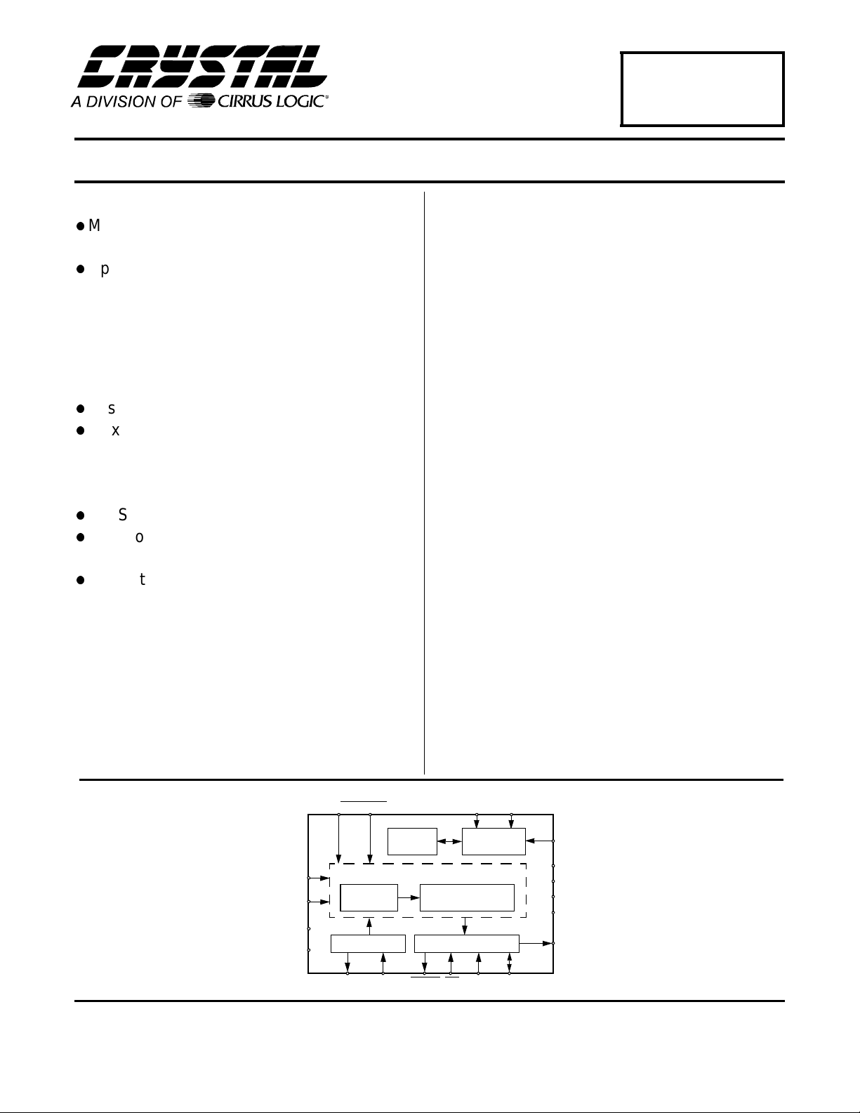
I
10
VREF
9
AIN
8
AGND
5
DGND
Cirrus Logic, Inc.
Crystal Semiconductor Products Division
P.O. Box 17847, Austin, Texas 78760
(512) 445 7222 FAX: (512) 445 7581
http://www.crystal.com
Each device’s serial port offers two general purpose
modes of operation for direct interface to shift registers
or synchronous serial ports of industry-standard microcontrollers. In addition, the CS5501’s serial port offers a
third, UART-compatible mode of asynchronous
communication.
ORDERING INFORMATION
See page 33.
BP/UPSLEEP
12 11 4
Calibration
SRAM
Charge-Balanced A/D Converter
Analog
Modulator
Clock Generator Serial Interface Logic
2 3 18 16 1 19
CLKOUTCLKIN DRDY CS MODESCLK
Low-Pass Digit al Filter
Copyright Cirrus Logic, I nc. 1997
SC1 SC2
Calibration
Microcontroller
6-Pole Gaussian
(All Rights Reserv ed)
13
14
15
20
7
6
CAL
VA+
VAVD+
VD-
SDATA
MAR ‘95
DS31F2
1
CS5501/CS5503
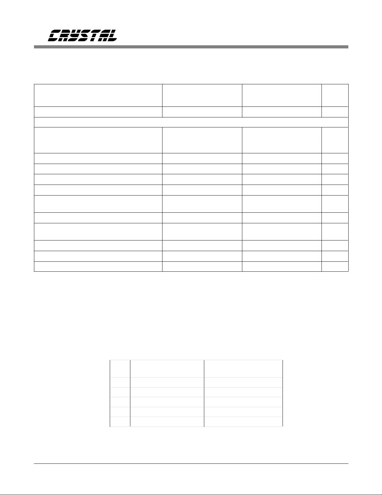
CS5501 ANALOG CHARACTERISTICS (T
VA-, VD- = -5V; VREF = 2.5V; CLKIN = 4.096MHz; Bipolar Mode; MODE = +5V; R
A
= T
MIN
to T
; VA+, VD+ = 5V;
MAX
source
= 750Ω with a 1nF
to AGND at AIN (see Note 1); Digital Inputs: Logic 0 = GND; Logic 1 = VD+; unless otherwise specified.)
CS5501-A, B, C CS5501-S, T
Parameter* Min Typ Max Min Typ Max Units
Specified Temperature Range -40 to +85 -55 to +125
°
C
Accuracy
Linearity Error -A, S
-B, T
-C
Differential Nonlinearity T
MIN
to T
MAX
Full Scale Error (Note 2) Full Scale Drift (Note 3) Unipolar Offset (Note 2) Unipolar Offset Drift (Note 3) -
-
0.0015
-
0.0007
-
0.0003
-
±
±
±
±
±
1/8
0.13
1.2
0.25
4.2
0.003
0.0015
-
-
-
0.0007
0.0012
±
1/2
±
0.5
--
±
1
-
-
-
±
1/8
±
0.13
±
2.3
±
0.25
--+3.0
0.003
0.0015
±
1/2
±
0.5
±
%FS
±
%FS
±
%FS
LSB
LSB
-LSB
±
LSB
1
-LSB
16
16
16
16
16
-25.0
Bipolar Offset (Note 2) Bipolar Offset Drift (Note 3) -
±
±
0.25
2.1
±
1
--+1.5
-
±
0.25
±
LSB
1
-LSB
16
16
-12.5
Bipolar Negative Full Scale Error (Note 2) Bipolar Negative Full Scale Drift (Note 3) -
±
0.5
±
0.6
±
2
--
-
±
0.5
±
1.2
±
LSB
2
-LSB
16
16
Noise (Referred to Output) - 1/10 - - 1/10 - LSBrms
Notes: 1. The AIN pin presents a very high input resistance at dc and a minor dynamic load which scales to the
master clock frequency. Both source resistance and shunt c apacitance are therefore critical in
determining the CS5501’s source impedance requirements. For more information refer the text section
Analog Input Impedance Considerations
.
2. Applies after calibration at the temperature of interest.
3. Total drift over the specified temperature range since calibration at power-up at 25°C (see Figure 11).
This is guaranteed by design and /or char acterization. Recalibration at any temperature will remove
these errors.
Unipolar Mode Bipolar Mode
µV LSB’s %FS ppm FS LSB’s %FS ppm FS
10 0.26 0.0004 4 0.13 0.0002 2
19 0.50 0.0008 8 0.26 0.0004 4
38 1.00 0.0015 15 0.50 0.0008 8
76 2.00 0.0030 30 1.00 0.0015 15
152 4.00 0.0061 61 2.00 0.0030 30
CS5501 Unit Conversion Factors, VREF = 2.5V
* Refer to the Specification Definitions immediately following the Pin Description Section.
2 DS31F2
CS5501/CS5503
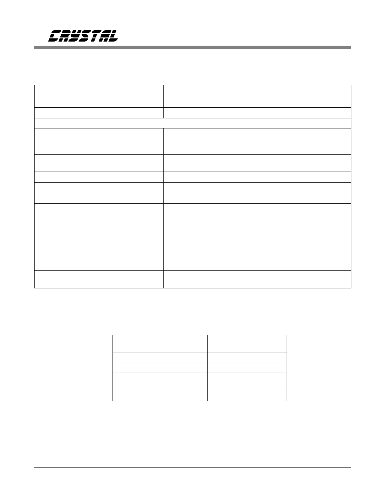
CS5503 ANALOG CHARACTERISTICS (T
VA-, VD- = -5V; VREF = 2.5V; CLKIN = 4.096MHz; Bipolar Mode; MODE = +5V; R
A
= T
MIN
to T
; VA+, VD+ = 5V;
MAX
source
= 750Ω with a 1nF
to AGND at AIN (see Note 1): unless otherwise specified.)
CS5503-A, B, C CS5503-S, T
Parameter* Min Typ Max Min Typ Max Units
Specified Temperature Range -40 to +85 -55 to +125
°
C
Accuracy
Linearity Error -A, S
-B, T
-C
Differential Nonlinearity T
MIN
to T
MAX
-
0.0015
-
0.0007
-
0.0003
0.003
0.0015
0.0012
-
-
-
0.0007
0.003
TBD
±
%FS
±
%FS
±
%FS
-20- -20-Bits
(Not Missing Codes)
Full Scale Error (Note 2) Full Scale Error Drift (Note 3) Unipolar Offset (Note 2) Unipolar Offset Drift (Note 3) -
±
4
±
19
±
4
±
67
±
16
--
±
16
--+48
-
-
±
4
±
37
±
4
±
16
±
16
LSB
-LSB
LSB
-LSB
-400
Bipolar Offset (Note 2) Bipolar Offset Drift (Note 3) -
±
4
±
34
±
16
--+24
-
±
4
±
16
LSB
-LSB
-200
Bipolar Negative Full Scale Error (Note 2) Bipolar Negative Full Scale Drift (Note 3) -
±
8
±
10
±
32
--
-
±
8
±
20
±
32-
LSB
-LSB
Noise (Referred to Output) - 1.6 - - 1.6 - LSBrms
(20)
20
20
20
20
20
20
20
20
Unipolar Mode Bipolar Mode
µ
V LSB’s %FS ppm Fs LSB’s %FS ppm FS
0.596 0.25 0.0000238 0.24 0.13 0.0000119 0.12
1.192 0.50 0.0000477 0.47 0.26 0.0000238 0.24
2.384 1.00 0.0000954 0.95 0.50 0.0000477 0.47
4.768 2.00 0.0001907 1.91 1.00 0.0000954 0.95
9.537 4.000 0.0003814 3.81 2.00 0.0001907 1.91
CS5503 Unit Conversion Factors, VREF = 2.5V
* Refer to the Specification Definitions immediately following the Pin Description Section.
DS31F2 3
CS5501/CS5503
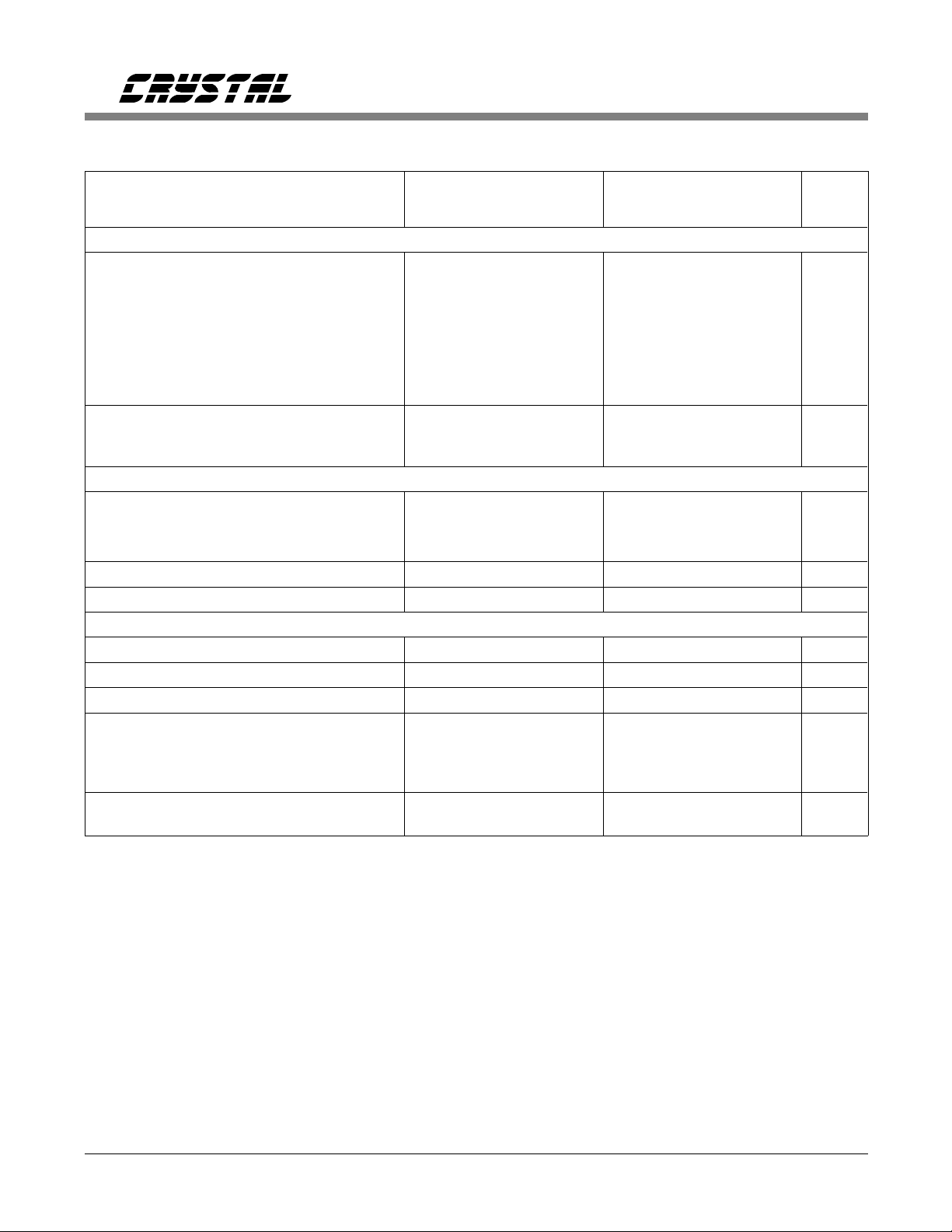
ANALOG CHARACTERISTICS (Continued)
CS5501/3-A, B, C CS5501/3-S, T
Parameter* Min Typ Max Min Typ Max Units
Power Supplies
DC Power Supply Currents
IA+
IAID+
ID- (Note 4)
Power Dissipation
SLEEP High
SLEEP Low (Note 4)
Power Supply Rejection
Positive Supplies
Negative Supplies (Note 5)
Analog Input
Analog Input Range
Unipolar
Bipolar Input Capacitance - 20 - - 20 - pF
DC Bias Current (Note 1) - 1 - - 1 - nA
System Calibration Specifications
Positive Full Scale Calibration Range VREF+0.1 VREF+0.1 V
Positive Full Scale Input Overrange VREF+0.1 VREF+0.1 V
Negative Full Scale Input Overrange -(VREF+0.1) -(VREF+0.1) V
Maximum Offset
Calibration Range (Notes 6, 7)
Unipolar Mode
Bipolar Mode
Input Span (Note 8) 80%
Notes: 4. All outputs unloaded.
5. 0.1Hz to 10Hz. PSRR at 60 Hz will exceed 120 dB due to the benefit of the digital filter.
6. In unipolar mode the offset can have a negative value (-VREF) such that the unipolar mode can mimic
bipolar mode operation.
7. The specifications for Input Overrange and for Input Span apply additional constraints on the offs et
calibration range.
8. For Unipolar mode, Input Span is the difference between full scale and zero scale. For Bipolar mode,
Input Span is the difference between positive and negative full scale points. When using less than
the maximum input span, the span range may be placed anywhere within the range of ±(VREF + 0.1).
-
-
-
-
-
-
-
-
-40%VREF to +40%VREF
VREF
2
2
1
0.03
25
10
70
75
0 to +2.5
±
2.5
-(VREF +0.1)
3.2
3.2
1.5
0.1
40
20
-
-
--
2VREF
+0.2
-
-
-
-
-
-
-
-
-40%VREF to +40%VREF
80%
VREF
2
2
1
0.03
25
10
70
75
0 to +2.5 V
±
2.5
-(VREF +0.1)
3.2
3.2
1.5
0.1
40
40
-
-
-V
2VREF
+0.2 V
mA
mA
mA
mA
mW
µ
W
dB
dB
V
V
Specifications are subject to change without notice.
4 DS31F2
DYNAMIC CHARACTERISTICS
CS5501/CS5503
Parameter Symbol
Sampling Frequency
Output Update Rate
Filter Corner Frequency
Settling Time to +0.0007% FS (FS Step)_
20
0
-20
-40
-60
-80
Output Amplitude in dB
-100
-120
CLKIN = 2 MHz
CLKIN = 1 MHz
f
s
f
out
f
-3dB
t
s
CLKIN = 4 MHz
CLKIN/ 256
CLKIN /1024
CLKIN /409,600
506,880/CLKIN
Ratio
Units
Hz
Hz
Hz
s
-σ
-140
1 10 100
-1-2
S-Domain Pole/Zero Plot (Continuous-Time Representation)
H(x) = [1 + 0.694x
where x = f /f
Continuous-Time Representation of 6-Pole Gaussian Filter
Frequency in Hz
1000
Frequency Response
jω
j2
j1
-j1
-j2
2
+ 0.241x4 + 0.0557x6 + 0.009664x8 + 0.00134x10 + 0.000155x12]
-3dB
, f
= CLKIN/409,600 , and f is the frequency of inter est.
-3dB
S
= -1.4667 ± j1.8199
1,2
S
= -1.7559 ± j1.0008
3,4
S
= -1.8746 ± j0.32276
5,6
-1/2
DS31F2 5
CS5501/CS5503
DIGITAL CHARACTERISTICS
(TA = T
min
to T
Parameter Symbol Min Typ Max Units
Calibration Memory Retention
Power Supply Voltage (VD+ and VA+)
High-Level Input Voltage All Except CLKIN V
High-Level Input Voltage CLKIN V
Low-Level Input Voltage All Except CLKIN V
Low-Level Input Voltage CLKIN V
High-Level Output Voltage (Note 9) V
Low-Level Output Voltage Iout=1.6mA V
Input Leakage Current I
3-State Leakage Current I
Digital Output Pin Capacitance C
Notes: 9. I
= -100 µA. This guarantees the ability to drive one TTL load. (VOH = 2.4V @ I
out
ABSOLUTE MAXIMUM RATINGS
Parameter Symbol Min Max Units
; VA+, VD+ = 5V ± 10%; VA-, VD- = -5V ± 10%)
max
V
MR
IH
IH
IL
IL
OH
OL
in
OZ
out
2.0 - - V
2.0 - - V
3.5 - - V
--0.8V
--1.5V
(VD+)-1.0V - - V
--0.4V
--10
--
±10µ
-9-pF
= -40 µA).
out
µ
A
A
DC Power Supplies: Positive Digital
Negative Digital
Positive Analog
Negative Analog
Input Current, Any Pin Except Supplies (Notes 10, 11) I
Analog Input Voltage (AIN and VREF pins) V
Digital Input Voltage V
Ambient Operating Temperature T
Storage Temperature T
VD+
VD-
VA+
VA-
in
INA
IND
A
stg
-0.3
0.3
-0.3
0.3
-
(VA+)+0.3
-6.0
6.0
-6.0
±
10
(VA-)-0.3 (VA+)+0.3 V
-0.3 (VA+)+0.3 V
-55 125 C°
-65 150 C°
Notes: 10. Applies to all pins including continuous overvoltage conditions at the analog input (AIN) pin.
11. Transient currents of up to 100mA will not cause SCR latch-up. Maximum input current for a power
supply pin is ± 50 mA.
V
V
V
V
mA
6 DS31F2
CS5501/CS5503
RECOMMENDED OPERATING CONDITIONS (AGND, DGND = 0V) (Note 12)
Parameter Symbol Min Typ Max Units
DC Power Supplies: Positive Digital
Negative Digital
Positive Analog
Negative Analog
VD+
VD-
VA+
VA-
4.5
-4.5
4.5
-4.5
5.0
-5.0
5.0
-5.0
VA+
-5.5
5.5
-5.5
Analog Reference Voltage VREF 1.0 2.5 3.0 V
Analog Input Voltage: (Note 13)
Unipolar
Bipolar
V
AIN
V
AIN
AGND
-VREF
-
-
VREF
VREF
Notes: 12. All voltages with respect to ground.
13. The CS5501 and CS5503 can accept input voltages up to the analog supplies (VA+ and VA-). They
will accurately convert and filter signals with noise excursions up to 100mV beyond |VREF|.
After filtering, the devices will output all 1’s for any input above VREF and all 0’s for any input below
AGND in unipolar mode and -VREF in bipolar mode.
SWITCHING CHARACTERISTICS
VA-, VD- = -5V ± 10%; Input Levels: Logic 0 = 0V, Logic 1 = VD+; C
(TA = T
min
to T
; CLKIN=4.096 MHz; VA+, VD+ = 5V±10%;
max
= 50 pF; unless otherwise specified.)
L
Parameter Symbol Min Typ Max Units
Master Clock Frequency: Internal Gate Oscillator
CLKIN
200
4096
5000
(See Table 1)
Externally Supplied: (Note 14)
Maximum
Minimum (Note 15)
CLKIN
CLKIN
-
200
40
-
5000
CLKIN Duty Cycle 20 - 80 %
Rise Times: Any Digital Input
Any Digital Output (Note 16)
Fall Times: Any Digital Input
Any Digital Output (Note 16)
Set Up Times: SC1, SC2 to CAL Low
SLEEP High to CLKIN High (Note 17)
Hold Time: SC1, SC2 hold after CAL falls t
t
rise
t
rise
t
t
t
scs
t
sch
fall
fall
sls
-
-
-
-
100
1
100 - - ns
20
20
-
1.0
-
-
1.0
-
-
-
-
-
V
V
V
V
V
V
kHz
kHz
kHz
µ
s
ns
µ
s
ns
ns
µ
s
Notes: 14. CLKIN must be supplied whenever the CS5501 or CS5503 is not in SLEEP mode. If no clock is
present when not in
SLEEP mode, the device can draw higher current than specified
and possibly become uncalibrated.
15. The CS5501/CS5503 is production tested at 4.096 MHz. It is guaranteed by characterization
to operate at 200 kHz.
16. Specified using 10% and 90% points on waveform of interest.
17. In order to synchronize several CS5501’s or CS5503’s together using the
SLEEP pin,
this specification must be met.
DS31F2 7
CS5501/CS5503
SWITCHING CHARACTERISTICS
(continued) (TA = T
VA-, VD- = -5V ± 10%; Input Levels: Logic 0 = 0V, Logic 1 = VD+; C
Parameter Symbol Min Typ Max Units
SSC Mode (Mode = VD+)
Access Time CS Low to SDATA Out t
SDATA Delay Time SCLK Falling to New SDATA bit t
SCLK Delay Time SDATA MSB bit to SCLK Rising
csd1
dd1
t
cd1
(at 4.096 MHz)
Serial Clock Pulse Width High (at 4.096 MHz)
(Out) Pulse Width Low
Output Float Delay SCLK Rising to Hi-Z t
Output Float Delay CS High to Output Hi-Z (Note 18) t
t
ph1
t
pl1
fd2
fd1
SEC Mode (Mode = DGND)
Serial Clock (In) f
Serial Clock (In) Pulse Width High
Pulse Width Low
Access Time CS Low to Data Valid (Note 19) t
sclk
t
ph2
t
pl2
csd2
Maximum Data Delay Time (Note 20)
SCLK Falling to New SDATA bit t
Output Float Delay CS High to Output Hi-Z t
Output Float Delay SCLK Falling to Output Hi-Z t
Notes: 18. If
CS is returned high before all data bits ar e output, the SDATA and S CLK outputs will complete
dd2
fd3
fd4
the current data bit and then go to high impedance.
CS is activated asynchronously to DRDY, CS will not be recognized if it occurs when DRDY is high
19. If
for 4 clock cycles. The propagation delay time may be as great as 4 CLKIN cycles plus 160 ns.
To guarantee proper clocking of SDATA when using asychronous
high sooner than 4 CLKIN cycles plus 160ns after
CS goes low.
20. SDATA transitions on the falling edge of SCLK(i).
to T
min
= 50 pF)
L
; VA+, VD+ = 5V ± 10%;
max
3/CLKIN - - ns
- 25 100 ns
250 380 - ns
-
-
- 1/CLKIN
240
730
+ 100
300
790
1/CLKIN
+ 200
--4/CLKIN
+200
dc - 4.2 MHz
50
180
-
-
-
-
- 80 160 ns
- 75 150 ns
- - 250 ns
- 100 200 ns
CS, SCLK(i) should not be taken
ns
ns
ns
ns
CAL
scstsch
SC1, SC2
Calibration Control Timing
t
VALID
CLKIN
SLEEP
Sleep Mode Timing for
Synchronization
CS
t
sls
SDATA
t
fd1
Output Float Delay
SSC Mode (Note 19)
8 DS31F2
CLKIN
CS
SDATA
SCLK (o)
t
csd1
Hi-Z Hi-ZMSB-2 LSBMSB MSB-1
t
dd1
t
cd1
Hi-Z
t
ph1
t
pl1
SSC MODE Timing Relationships
CS5501/CS5503
t
fd2
Hi-Z
DRDY
CS
SDATA
SCLK (i)
CS
SDATA
SCLK (i)
t
csd2
Hi-Z MSB MSB-1
t
t
dd2
dd2
t
ph2
t
csd2
Hi-Z Hi-ZLSBMSB MSB-1
t
dd2
t
ph2
SEC MODE Timing Relationships
t
fd4
t
t
pl2
fd3
Hi-Z
DS31F2 9
CS5501/CS5503
SWITCHING CHARACTERISTICS (continued) (T
A
= T
min
to T
max
;
VA+, VD+ = 5V ± 10%; VA-, VD- = -5V ± 10%; Input Levels: Logic 0 = 0V, Logic 1 = VD+; C
Parameter Symbol Min Typ Max Units
AC Mode (Mode = VD-) CS5501 only
Serial Clock (In) f
Serial Clock (In) Pulse Width High
Pulse Width Low
Set-up Time CS Low to SCLK Falling t
Maximum Data Delay Time SCLK Fall to New SD ATA bit t
Output Float Delay CS High to Output Hi-Z (Note 21) t
Notes: 21. If
CS is returned high after an 11-bit data pac ket is started, the SDATA output will continue to output
sclk
t
ph3
t
pl3
css
dd3
fd5
dc - 4.2 MHz
50
180
-
-
-2040ns
- 90 180 ns
- 100 200 ns
data until the end of the second stop bit. At that time the SDATA output will go to high impedance.
= 50 pF)
L
-
-
ns
ns
DRDY
CS
SCLK(i)
SDATA
t
css
t
dd3
Hi-Z Hi-ZBIT7BIT6BIT9
START
BIT8
High Byte
t
AC MODE Timing Relationships (CS5501 only)
t
ph3
pl3
Low Byte
STOP1
STOP2
t
fd5
10 DS31F2
CS5501/CS5503
GENERAL DESCRIPTION
The CS5501/CS5503 are monolithic CMOS A/D
converters designed specifically for high resolution measurement of low-frequency signals. Each
device consists of a charge-balance converter (16Bit for the CS5501, 20-Bit for the CS5503),
calibration microcontroller with on-chip SRAM,
and serial communications port.
The CS5501/CS5503 A/D converters perform
conversions continuously and update their output
ports after every conversion (unless the serial port
is active). Conversions are performed and the serial port is updated independent of external
control. Both devices are capable of measuring
either unipolar or bipolar input signals, and calibration cycles may be initiated at any time to
ensure measurement accuracy.
The CS5501/CS5503 perform conversions at a
rate determined by the master clock signal. The
master clock can be set by an external clock or
with a crystal connected to the pins of the on-chip
gate oscillator. The master clock frequency determines:
1. The sample rate of the analog input signal.
2. The corner frequency of the on-chip digital
filter.
3. The output update rate of the serial output port.
The CS5501/CS5503 design includes several selfcalibration modes and several serial port interface
modes to offer users maximum system design
flexiblity.
The Delta-Sigma Conversion Method
The CS5501/CS5503 A/D converters use chargebalance techniques to achieve low cost, high
resolution measurements. A charge-balance A/D
converter consists of two basic blocks: an analog
modulator and a digital filter. An elementary example of a charge-balance A/D converter is a
conventional voltage-to-frequency converter and
counter. The VFC’s 1-bit output conveys infor-
mation in the form of frequency (or duty cycle),
which is then filtered (averaged) by the counter
for higher resolution.
LP Filter
S/H Amp
Figure 1. Charge Balance (Delta-Sigma) A/D Converter
Comparator
DAC
1-bit
Digital Filter
16-bits
The analog modulator of the CS5501/CS5503 is a
multi-order delta-sigma modulator. The modulator
consists of a 1-bit A/D converter (that is, a comparator) embedded in an analog feedback loop
with high open loop gain (see Figure 1). The
modulator samples and converts the input at a rate
well above the bandwidth of interest. The 1-bit
output of the comparator is sampled at intervals
based on the clock rate of the part and this information (either a 1 or 0) is conveyed to the digital
filter. The digital filter is much more sophisticated
than a simple counter. The filter on the chip has a
6-pole low pass Gaussian response which rolls off
at 120 dB/decade (36 dB/octave). The corner frequency of the digital filter scales with the master
clock frequency. In comparison, VFC’s and dual
slope converters offer (sin x)/x filtering for high
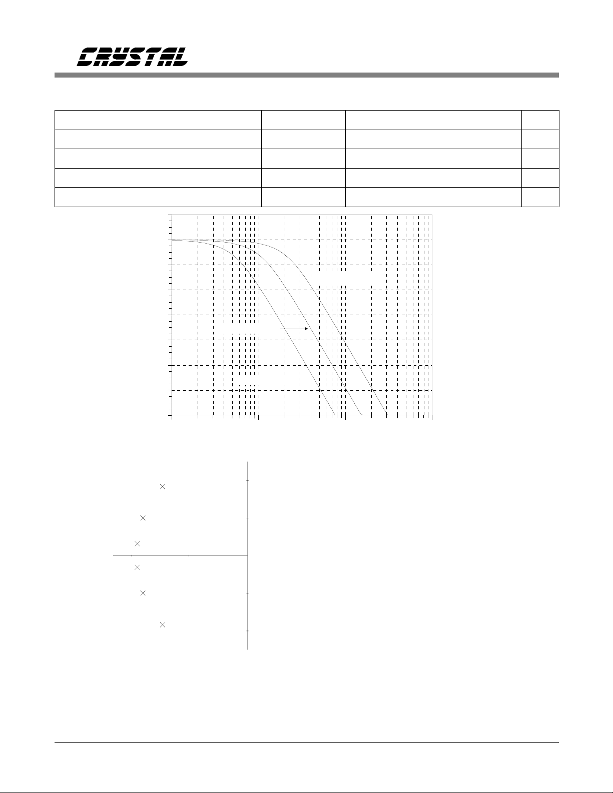
frequency rejection (see Figure 2 for a comparison of the characteristics of these two filter types).
When operating from a 1 MHz master clock the
digital filter in the CS5501/CS5503 offers better
than 120 dB rejection of 50 and 60 Hz line frequencies and does not require any type of line
synchronization to achieve this rejection. It should
be noted that the CS5501/CS5503 will update its
output port almost at 1000 times per second when
operating from the 1 MHz clock. This is a much
higher update rate (typically by a factor of at least
50 times) than either VFCs or dual-slope converters can offer.
For a more detailed discussion on the delta-sigma
modulator see the Application note "Delta-Sigma
DS31F2 11
CS5501/CS5503
Magnitude (dB)
-100
-20
-40
-60
-80
0
0
20
40 60 80 100
Frequency (Hz)
0
-20
-40
-60
Magnitude (dB)
-80
-100
CLKIN = 4 MHz
CLKIN = 2 MHz
CLKIN=1 MHz
0
20 40 60 80 10 0
Frequency (Hz)
a. Averaging (Integrating) Filter Response (tavg = 100 ms) b. 6-Pole Gaussian Filter Response
Figure 2. Filter Responses
A/D Conversion Technique Overview" in the ap-
Clock Generator
plication note section of the data book. The
application note discusses the delta-sigma modulator and some aspects of digital filtering.
The CS5501/CS5503 both include gates which
can be connected as a crystal oscillator to provide
the master clock signal for the chip. Alternatively,
an external (CMOS compatible) clock can be in-
OVERVIEW
put to the CLKIN pin as the master clock for the
device. Figure 3 illustrates a simple model of the
As shown in the block diagram on the front page
of the data sheet, the CS5501/CS5503 can be segmented into five circuit functions. The heart of the
chip is the charge balance A/D converter (16-bit
for the CS5501, 20-bit for the CS5503). The con-
on-chip gate oscillator. The gate has a typical
transconductance of 1500 µmho. The gate model
includes 10 pf capacitors at the input and output
pins. These capacitances include the typical stray
capacitance of the pins of the device. The on-chip
verter and all of the other circuit functions on the
500 k
chip must be driven by a clock signal from the
R
1
clock generator. The serial interface logic outputs
the converted data. The calibration microcontroller along with the calibration SRAM (static
RAM), supervises the device calibration. Each
segment of the chip has control lines associated
CLKIN CLKOUT
3
10pF
g
1500 umho
m
with it. The function of each of the pins is described in the pin description section of the data
sheet.
C1 * Y1 C2 *
* See Table 1
Ω
2
10pF
Figure 3. On-chip Gate Oscillator Model
12 DS31F2
CS5501/CS5503
gate oscillator is designed to properly operate
without additional loading capacitors when using
a 4.096 MHz (or 4 MHz) crystal. If other crystal
frequencies or if ceramic resonators are used,
loading capacitors may be necessary for reliable
operation of the oscillator. Table 1 illustrates some
typical capacitor values to be used with selected
resonating elements.
C1 C2Resonators
Ceramic
330pF 470pF200 kHz
100pF 100pF455 kHz
50pF 50pF1.0 MHz
20pF 20pF2.0 MHz
Crystals
30pF 30pF2.000 MHz
20pF 20pF3.579 MHz
None None4.096 MHz
Table 1. Resonator Loading Capacitors
CLKOUT (pin 2) can be used to drive one external CMOS gate for system clock requirements. In
this case, the external gate capacitance must be
taken into account when choosing the value of
C2.
Caution: A clock signal should always be present
whenever the SLEEP is inactive (SLEEP = VD+).
If no clock is provided to the part when not in
SLEEP, the part may draw excess current and
possibly even lose its calibration data. This is because the device is built using dynamic logic.
Serial Interface Logic
The CS5501 serial data output can operate in any
one of the following three different serial interface
modes depending upon the MODE pin selection:
SSC (Synchronous Self-Clocking) mode;
MODE pin tied to VD+ (+5V).
SEC (Synchronous External Clocking) mode;
MODE pin tied to DGND.
and AC (Asynchronous Communication) mode;
CS5501 only
MODE pin tied to VD- (-5V)
The CS5503 can only operate in the first two
modes, SEC and SSC.
Synchronous Self-Clocking Mode
When operated in the SSC mode (MODE pin tied
to VD+), the CS5501/CS5503 furnish both serial
output data (SDATA) and an internally-generated
serial clock (SCLK). Internal timing for the SSC
mode is illustrated in Figure 4. Figure 5 shows
detailed SSC mode timing for both the
CS5501/CS5503. A filter cycle occurs every 1024
cycles of CLKIN. During each filter cycle, the
status of CS is polled at eight specific times dur-
ing the cycle. If CS is low when it is polled, the
CS5501/CS5503 begin clocking the data bits out,
MSB first, at a SCLK output rate of CLKIN/4.
Once transmission is complete, DRDY rises and
both SDATA and SCLK outputs go into a high
impedance state. A filter cycle begins each time
DRDY falls. If the CS line is not active, DRDY
will return high 1020 clock cycles after it falls.
Four clock cycles later DRDY will fall to signal
that the serial port has been updated with new
data and that a new filter cycle has begun. The
first CS polling during a filter cycle occurs 76
clock cycles after DRDY falls (the rising edge of
CLKIN on which DRDY falls is considered clock
cycle number one). Subsequent pollings of CS oc-
cur at intervals of 128 clock cycles thereafter (76,
204, 332, etc.). The CS signal is polled at the be-
ginning of each of eight data output windows
which occur in a filter cycle. To transmit data dur-
ing any one of the eight output windows, CS must
be low at least three CLKIN cycles before it is
polled. If CS does not meet this set-up time, data
will not be transmitted during the window time.
Furthermore, CS is not latched internally and
therefore must be held low during the entire data
transmission to obtain all of the data bits.
DS31F2 13
Internal
Status
64/CLKIN
Note 1
Analog Time 0 Digital Time 0
64/CLKIN
f
=1024/CLKIN
out
Analog Time 1 Digital Time1
CS5501/CS5503
76/CLKIN
DRDY (o)
CS (i)
CS5501
SCLK (o)
CS5501
SDATA (o)
CS5503
SCLK (o)
CS5503
SDATA (o)
Note: 1. There are 16 analog and digital settling periods per filter cycle (4 are s hown). Data can be output in the
SSC mode in only 1 of the 8 digital time periods in each filter cycle.
CLKIN (i )
Hi-Z
Hi-Z
Hi-Z
Hi-Z
76 CLKIN cycles
CS Polled
(MSB)
(MSB) (LSB)
Figure 4. Internal Timing
(LSB)
Hi-Z
Hi-Z
Hi-Z
Hi-Z
DRDY (o)
CS (i)
(MSB) (LSB)
SDATA (o)
SCLK (o)
*
CS5501
**
CS5503
Hi-Z B0B1 Hi-Z
Figure 5. Synchronous Self-Clocking (SSC) Mode Timing
B15*
B19**
The eighth output window time overlaps the time
in which the serial output port is to be updated. If
B14*
B18**
Hi-ZHi-Z
(CLKIN = 4.096 MHz) instead of the normal
4 kHz serial port update rate.
the CS is recognized as being low when it is
polled for the eighth window time, data will be
output as normal, but the serial port will not be
updated with new data until the next serial port
update time. Under these conditions, the serial
port will experience an update rate of only 2 kHz
14 DS31F2
Upon completion of transmission of all the data
bits, the SCLK and SDATA outputs will go to a
high impedance state even with CS held low. In
the event that CS is taken high before all data bits
are output, the SDATA and SCLK outputs will

CS5501/CS5503
complete the current data bit output and go to a
high impedance state when SCLK goes low.
Synchronous External Clocking Mode
When operated in the SEC mode (MODE pin tied
to DGND), the CS5501/CS5503 outputs the data
in its serial port at a rate determined by an external clock which is input into the SCLK pin. In
this mode the output port will be updated every
1024 CLKIN cycles. DRDY will go low when
new data is loaded into the output port. If CS is
not active, DRDY will return positive 1020
CLKIN cycles later and remain so for four
CLKIN cycles. If CS is taken low it will be recognized immediately unless it occurs while
DRDY is high for the four clock cycles. As soon
as CS is recognized, the SDATA output will come
out of its high-impedance state and present the
MSB data bit. The MSB data bit will remain present until a falling edge of SCLK occurs to
advance the output to the MSB-1 bit. If the CS
and external SCLK are operated asynchronously
to CLKIN, errors can result in the output data unless certain precautions are taken. If CS is
activated asynchronously, it may occur during the
four clock cycles when DRDY is high and therefore not be recognized immediately. To be certain
that data misread errors will not result if CS occurs at this time, the SCLK input should not
transition high to latch the MSB until four
CLKIN cycles plus 160 ns after CS is taken low.
This insures that CS will be recognized and the
MSB bit will become stable before the SCLK
transitions p ositive t o latch the M SB data bit.
When SCLK returns low the serial port will pre-
sent the MSB-1 data bit on its output.
Subsequent cycles of SCLK will advance the data
output. When all data bits are clocked out, DRDY
will then go high and the SDATA output will go
into a high impedance state. If the CS input goes
low and all of the data bits are not clocked out of
the port, filter cycles will continue to occur but
the output serial port will not be updated with
new data (DRDY will remain low). If CS is taken
high at any time, the SDATA output pin will go to
a high impedance state. If any of the data bits in
the serial port have not been clocked out, they
will remain available until DRDY returns high for
four clock cycles. After this DRDY will fall and
the port will be updated with a new 16-bit word
in the CS5501 or 20-bit word in the CS5503. It
is acceptable to clock out less than all possible
data bits if CS is returned high to allow the port
to be updated. Figure 6 illustrates the serial port
timing in the SEC mode.
Asynchronous Communication Mode (CS5501
Only)
In the CS5501, the AC mode is activated when
the MODE pin is tied to VD- (-5 V). When oper-
ating in the AC mode the CS5501 is designed to
DRDY (o)
CS (i)
SCLK (i)
(MSB)
SDATA (o)
DS31F2 15
Hi-Z
CS5501
*
**
CS5503
Figure 6. Synchronous External-Clocking (SEC) Mode Timing
B15* B14*
B19** B18**
(LSB)
B0B1
Hi-Z
CS5501/CS5503
provide data output in UART compatible format.
The baud rate of the SDATA output will be determined by the rate of the SCLK input. The data
which is output of the SDATA pin will be formatted such that it will contain two 11 bit data
packets. Each packet includes one start bit, eight
data bits, and two stop bits. The packet which carries the most-significant-byte data will be output
first, with its lsb being the first data bit output
after the start bit.
In this mode, DRDY will occur every 1024 clock
cycles. If the serial port is not outputting a data
byte, DRDY will return high after 1020 clock cycles and remain high for 4 clock cycles. DRDY
will then go low to indicate that an update to the
serial output port with a new 16 bit word has occurred. To initiate a transmission from the port the
CS line must be taken low. Then SCLK, which is
an input in this mode, must transition from a high
to a low to latch the state of CS internal to the
CS5501. Once CS is recognized and latched as a
low, the port will begin to output data. Figure 7
details the timing for this output. CS can be returned high before the end of the 11-bit
transmission and the transmission will continue
until the second stop bit of the first 11-bit packet
is output. The SDATA output will go into a high
impedance state after the second stop bit is output.
To obtain the second 11-bit packet CS must again
be brought low before DRDY goes high or the
second 11-bit data packet will be overwritten with
a serial port update. For the second 11-bit packet,
CS need only to go low for 50 ns; it need not be
latched by a falling edge of SCLK. Alternately,
the CS line can be taken low and held low until
both 11-bit data packets are output. This is the
preferred method of control as it will prevent los-
ing the second 11-bit data packet if the port is
updated. Some serial data rates can be quite slow
compared to the rate at which the CS5501 can up-
date its output port. A slow data rate will leave
only a short period of time to start the second 11-
bit packet if CS is returned high momentarily. If
CS is held low continuously (CS hard-wired to
DGND), the serial port will be updated only after
all 22 bits have been clocked out of the port.
Upon the completion of a transmission of the two
11-bit data packets the SDATA output will go into
a high impedance state. If at any time during
transmission the CS is taken back high, the cur-
rent 11-bit data packet will continue to be output.
At the end of the second stop bit of the data
packet, the SDATA output will go into a high im-
pedance state.
Linearity Performance
The CS5501/CS5503 delta-sigma converters are
like conventional charge-balance converters in
that they have no source of nonmonotonicity. The
devices therefore have no missing codes in their
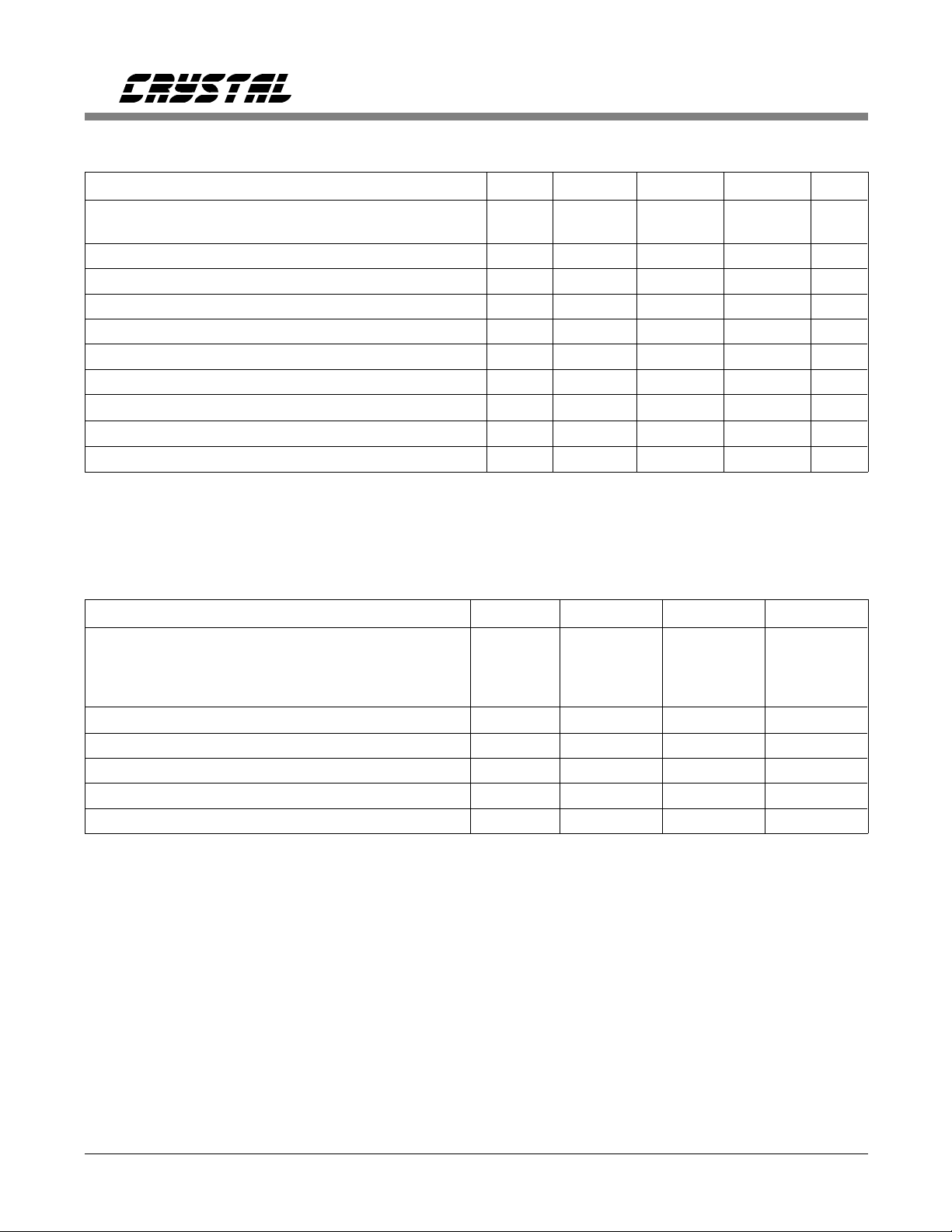
transfer functions. See Figure 8 for a plot of the
SCLK (i)
DRDY (o)
CS (i)
Stop
SDATA (o)
16 DS31F2
Hi-Z Start B8 B9 B14 B15 Start B0 B1 B6 B7
Figure 7. CS5501 Asynchronous (UART) Mode Timing
Stop
12
StopStop
12
CS5501/CS5503
+1
+1/2
0
DNL (LSB)
-1/2
-1
0 65,535
Figure 8. CS5501 Differential Nonlinearity Plot
32,768
Codes
excellent differential linearity achieved by the
CS5501. The CS5501/CS5503 also have excellent
integral linearity, which is accomplished with a
well-designed charge-balance architecture. Each
device also achieves low input drift through the
use of chopper-stabilized techniques in its input
stage. To assure that the CS5501/CS5503 achieves
excellent performance over time and temperature,
it uses digital calibration techniques to minimize
offset and gain errors to typically within ±1/2
LSB at 16 bits in the CS5501 and ±4 LSB at 20
bits in the CS5503.
Converter Calibration
The CS5501/CS5503 offer both self-calibration
and system level calibration capability. To understand the calibration features, a basic
comprehension of the internal workings of the
converter are helpful. As mentioned previously in
this data sheet, the converter consists of two sections. First is the analog modulator which is a
delta-sigma type charge-balance converter. This
is followed by a digital filter. The filter circuitry
is actually an arithmetic logic unit (ALU) whose
architecture and instructions execute the filter
function. The modulator (explained in more detail in the applications note "Delta-Sigma
Conversion Technique Overview") uses the VREF
voltage connected to pin 10 to determine the magnitude of the voltages used in its feedback DAC.
The modulator accepts an analog signal at its in-
put and produces a data stream of 1’s and 0’s as
its output. This data stream value can change
(from 1 to 0 or vice versa) every 256 CLKIN cycles. As the input voltage increases the ratio of
1’s to 0’s out of the modulator increases proportionally. The 1’s density of the data stream out of
the modulator therefore provides a digital representation of the analog input signal where the 1’s
density is defined as the ratio of the number of 1’s
to the number of 0’s out of the modulator for a
given period of time. The 1’s density output of the
modulator is also a function of the voltage on the
VREF pin. If the voltage on the VREF pin increases in value (say, due to temperature drift), and
the analog input voltage into the modulator remains
constant, the 1’s density output of the modulator will
decrease (less 1’s will occur). The analog input into
the modulator which is necessary to produce a given
binary output code from the converter is ratiometric
to the voltage on the VREF pin. This means that if
VREF increases by one per cent, the analog signal
on AIN must also increase by one per cent to m aintain the same binary output code from the converter.
For a complete calibration to occur, the calibration
microcontroller inside the device needs to record
the data stream 1’s density out of the modulator
for two different input conditions. First, a "zero
scale" point must be presented to the modulator.
Then a "full scale" point must be presented to the
modulator. In unipolar self-cal mode the zero
scale point is AGND and the full scale point is the
voltage on the VREF pin. The calibration microcontroller then remembers the 1’s density out of
the modulator for each of these points and calcu-
lates a slope factor (LSB/µV). This slope factor
DS31F2 17

CS5501/CS5503
represents the gain slope for the input to output
transfer function of the converter. In unipolar
mode the calibration microcontroller determines
the slope factor by dividing the span between the
zero point and the full scale point by the total
resolution of the converter (216 for the CS5501,
resulting in 65,536 segments or 220 for the
CS5503, resulting in 1,048,578 segments). In bipolar mode the calibration microcontroller divides
the span between the zero point and the full scale
point into 524,288 segments for the CS5503 and
32,768 segments for the CS5501. It then extends
the measurement range 524,288 segments for the
CS5503, 32,768 segments for the CS5501, below
the zero scale point to achieve bipolar measurement capability. In either unipolar or bipolar
modes the calculated slope factor is saved and
later used to calculate the binary output code
when an analog signal is present at the AIN pin
during measurement conversions.
Figure 9). System calibration performs the same
slope factor calculations as self cal but uses voltage values presented by the system to the AIN pin
for the zero scale point and for the full scale
point. Table 2 depicts the calibration modes
available. Two system calibration modes are
listed. The first mode offers system level calibration for system offset and for system gain. This is
a two step calibration. The zero scale point (system offset) must be presented to the converter
first. The voltage that represents zero scal e point
must be input to the converter before the calibration step is initiated and must remain stable until
the step is complete. The DRDY output from the
converter will signal when the step is complete by
going low. After the zero scale point is calibrated,
the voltage representing the full scale point is input to the converter and the second calibration
step is initiated. Again the voltage must remain
stable throughout the calibration step.
System calibration allows the A/D converter to
compensate for system gain and offset errors (see
VREF
Transducer
* DRDY remains high throughout the calibration sequence. In Self-Cal mode (SC1 and SC2 low) DRDY
falls once the CS5501 or CS5503 has settled to the analog input. In all other modes
immediately after the calibration term has been determined.
sys
Analog
MUX
A0 A1
Figure 9. System Calibration
0 Self-Cal 3,145,655/f
1 1,052,5 99/f
0 1,068, 8 13/f
1 Syste m Offset 2,117,389/f
0
1
1
0
System Offset
& System Gain
Table 2. Calibration Control
Signal
Conditioning
Circuitry
This two step calibration mode offers another calibration feature. After a two step calibration
CS5501
CS5503
CAL SC1
SequenceFS CalZS CalSC2SC1CAL Cal Type Calibrat ion Time
One StepVREFAGND
1st Step-AIN
2nd StepAINOne StepVREFAIN
SCLK
SDATA
SC2
CLK
DATA
µ
C
I/O 1
I/O 2
I/O 3
I/O 4
I/O 5
clk
clk
clk
clk
DRDY falls
18 DS31F2

CS5501/CS5503
sequence (system offset and system gain) has
been properly performed, additional offset calibrations can be performed by themselves to
reposition the gain slope (the slope factor is not
changed) to adjust its zero reference point to the
new system zero reference value.
A second system calibration mode is available
which uses an input voltage for the zero scale
calibration point, but uses the VREF voltage as
the full scale calibration point.
Whenever a system calibration mode is used,
there are limits to the amount of offset and to the
amount of span which can be accommodated.
The range of input span which can be accommodated in either unipolar or bipolar mode is
restricted to not less than 80% of the voltage on
VREF and not more than 200% of (VREF +
0.1) V. The amount of offset which can be calibrated depends upon whether unipolar or bipolar
mode is being used. In unipolar mode the system
calibration modes can handle offsets as positive as
20% of VREF (this is restricted by the minimum
span requirement of 80% VREF) or as negative as
-(VREF + 0.1) V. This capability enables the
unipolar mode of the CS5501/CS5503 to be calibrated to mimic bipolar mode operation.
In the bipolar mode the system offset calibration
range is restricted to a maximum of ±40% of
VREF. It should be noted that the span restrictions
limit the amount of offset which can be calibrated.
The span range of the converter in bipolar mode
extends an equidistance (+ and -) from the voltage
used for the zero scale point. When the zero scale
point is calibrated it must not cause either of the
two endpoints of the bipolar transfer function to
exceed the positive or the negative input overrange points (+(VREF + 0.1) V or - (VREF +
0.1) V). If the span range is set to a minimum
(80% VREF) the offset voltage can move ±40%
VREF without causing the end points of the transfer function to exceed the overrange points.
Alternatively, if the span range is set to 200% of
VREF, the input offset cannot move more than
+0.1 or 0.1 V before an endpoint of the transfer
function exceeds the input overrange limit.
Initiating Calibration
Table 2 illustrates the calibration modes available
in the CS5501/CS5503. Not shown in the table is
the function of the BP/UP pin which determines
whether the converter is calibrated to measure bipolar or unipolar signals. A calibration step is
initiated by bringing the CAL pin (13) high for at
least 4 CLKIN cycles to reset the part and then
bringing CAL low. The states of SC1 (pin 4) and
SC2 (pin 17) along with the BP/UP (pin 12) will
determine the type of calibration to be performed.
The SC1 and SC2 inputs are latched when CAL
goes low. The BP/UP input is not latched and
therefore must remain in a fixed state throughout
the calibration and measurement cycles. Any time
the state of the BP/UP pin is changed, a new calibration cycle must be performed to enable the
CS5501/CS5503 to properly function in the new
mode.
When a calibration step is initiated, the DRDY
signal will go high and remain high until the step
is finished. Table 2 illustrates the number of
clock cycles each calibration requires. Once a
calibration step is initiated it must finish before a
new calibration step can be executed. In the two
step system calibration mode, the offset calibration step must be initiated before initiating the
gain calibration step.
When a self-cal is completed DRDY falls and the
output port is updated with a data word that represents the analog input signal at the AIN pin.
When a system calibration step is completed,
DRDY will fall and the output port will be updated with the appropriate data value (zero scale
point, or full scale point). In the system calibration mode, the digital filter must settle before the
output code will represent the value of the analog
input signal.
DS31F2 19

CS5501/CS5503
1LSB
Cal Mode Zero Scale G ain Factor
CS5501 CS5503 CS5501 CS5503
VREF
Self-Cal AGND VREF
System Cal SOFF SGA IN
Table 3. Output Code Size After Calibration
Input Voltage, Unipolar Mode Input Voltage, B ipolar Mode
System-Cal Self-Cal
>(SGAIN - 1.5 LSB) >(VREF - 1. 5 LSB) FFFF FFFFF >( VREF - 1.5 LSB) >(SGAIN - 1.5 LSB)
SGAIN - 1.5 LSB VREF - 1.5 LSB
(SGAIN - SOFF)/2 - 0.5 LSB V REF/ 2 - 0.5 LS B
SOFF + 0.5 LSB AGND + 0.5 LSB
<(SOFF + 0.5 LSB) <(AGND+0.5 LSB) 0000 00000 <(-VREF+0.5 LSB) <(-SGAIN+2SOFF+0.5 LSB)
65,536
SGAIN−
65,536
Output Codes (Hex)
CS5501 CS5503
FFFF
FFFE
8000
7FFF
0001
0000
Table 4. Output Coding
Tables 3 and 4 indicate the output code size and
Unipolar Bipolar
SOFF
VREF
1,048,526
SGAIN−SOFF
1,048,526
FFFFF
FFFFE
80000
7FFFF
00001
00000
Self-Cal System Cal
VREF - 1.5 LSB SGAIN - 1.5 LSB
AGND - 0.5 LSB SOFF -0.5 LSB
-VREF+ 0.5 LSB -SGAIN + 2SOFF + 0.5 LSB
2VREF
65,536
2(SGA IN−SOFF)
65,536
Underrange And Overrange Considerations
2VREF
1,048,526
2(SGAIN−SOFF)
1,048,526
output coding of the CS5501/CS5503 in its various modes. The calibration equations which
represent the CS5501/CS5503 transfer function
are shown in Figure 10.
The input signal range of the CS5501/CS5503
will be determined by the mode in which the part
is calibrated. Table 4 indicates the input signal
range in the various modes of operation. If the
input signal exceeds the full scale point the converter will output all ones. If the signal is less
DOUT = Slope (AIN - Unipolar Offset) + 0.5 LSB
than the zero scale point (in unipolar) or more
negative in magnitude than minus the full scale
a. Unipolar Calibration
point (in bipolar) it will output all zeroes.
Note that the modulator-filter combination in the
CS5501
DOUT = Slope (AIN - Bipolar Offset) + 2
15
+ 0.5 LSB
16
chip CS5501/CS5503 is designed to accurately
convert and filter input signals with noise excursions which extend up to 100 mV below the
CS5503
DOUT = Slope(AIN - Bipolar Offset) + 2
19
+ 0.5 LSB
20
analog value which produces all zeros out or
above the analog value which produces all ones
out. Overrange noise excursions greater than
b. Bipolar Calibration
100 mV may increase output noise.
All pins of the CS5501/CS5503 include diodes
Figure 10. Calibration Equations
which clamp the input signals to within the positive and negative supplies. If a signal on any pin
(including AIN) exceeds the supply voltage (either
20 DS31F2

CS5501/CS5503
+ or -) a clamp diode will be forward-biased. Under these fault conditions the CS5501/CS5503
might be damaged. Under normal operating conditions (with the power supplies established), the
device will survive transient currents through the
clamp diodes up to 100 mA and continuous currents up to 10 mA. The drive current into the AIN
pin should be limited to a safe value if an overvoltage condition is likely to occur. See the
application note "Buffer Amplifiers for the
CS501X Series of A/D Converters" for further
discussion on the clamp diode input structure and
on current limiting circuits.
System Synchronization
If more than one CS5501/CS5503 is included in a
system which is operating from a common clock,
all of the devices can be synchronized to sample
and output at exactly the same time. This can be
accomplished in either of two ways. First, a si ngle
CAL signal can be issued to all the
CS5501/CS5503’s in the system. To insure synchronization on the same clock signal the CAL
signal should go low on the falling edge of
CLKIN. Or second, a common SLEEP control
signal can be issued. If the SLEEP signal goes
positive with the appropriate set up time to
CLKIN, all parts will be synchronized on the
same clock cycle.
Analog Input Impedance Considerations
The analog input of the CS5501/CS5503 can be
modeled as illustrated in Figure 11. A 20 pF capacitor is used to dynamically sample the input
signal. Every 64 CLKIN cycles the switch alternately connects the capacitor to the output of the
buffer and then directly to the AIN pin. Whenever the sample capacitor is switched from the
output of the buffer to the AIN pin, a small packet
of charge (a dynamic demand of current) will be
required from the input source to settle the voltage on the sample capacitor to its final value.
The voltage at the output of the buffer may differ
up to 100 mV from the actual input voltage due to
CS5501
AIN
AGND
Figure 11. Analog Input Model
CS5503
+
-
V 100 mv
≤
os
20 pF
the offset voltage of the buffer. Timing allows 64
cycles of master clock (CLKIN) for the voltage
on the sample capacitor to settle to its final value.
The equation which defines settling time is:
−
t
⁄
Ve = V
max
Where Ve is the final settled value, V
e
RC
max
is the
maximum error voltage value of the input signal,
R is the value of the input source resistance, C is
the 20 pF sample capacitor plus the value of any
stray or additional capacitance at the input pin.
The value of t is equal to 64/CLKIN.
V
occurs the instance when the sample capaci-
max
tor is switched from the buffer output to the AIN
pin. Prior to the switch, AIN has an error estimated as being less than or equal to Ve. V
max
is
equal to the prior error (Ve) plus the additional
error from the buffer offset. The estimate for
V
is:
max
20pF
(20pF+C
EXT)
Where C
V
= Ve+100mV
max
is the combination of any external
EXT
or stray capacitance.
From the equation which defines settling time, an
equation for the maximum acceptable source resistance is derived
DS31F2 21

CS5501/CS5503
equation which defines settling time, an equation
for the maximum acceptable source resistance is
derived
EXT
−64
) ln
Ve +
V
e
20pF(100mv)
( 20pF+C
Rs
=
max
CLKIN (20pF+C
This equation assumes that the offset voltage of
the buffer is 100 mV, which is the worst case.
The value of Ve is the maximum error voltage
which is acceptable.
For a maximum error voltage (Ve) of 10 µV in
the CS5501 (1/4LSB at 16-bits) and 600 nV in
the CS5503 (1/4LSB at 20-bits), the above equation indicates that when operating from a
4.096 MHz CLKIN, source resistances up to
84 kΩ in the CS5501 or 64 kΩ in the CS5503 are
acceptable in the absence of external capacitance
(C
= 0). If higher input source resistances
EXT
are desired the master clock rate can be reduced
to yield a longer settling time for the 64 cycle period.
10
5
0
-5
-10
EXT
160
80
0
-80
-160
)
drift. Charge injection in the analog switches and
leakage currents at the sampling node are the primary sources of offset voltage drift in the
converter. Figure 12 indicates the typical offset
drift due to temperature changes experienced after
calibration at 25 °C. Drift is relatively flat up to
about 75 °C. Above 75 °C leakage current be-
comes the dominant source of offset drift.
Leakage currents approximately double with each
10 °C of temperature increase. Therefore the off-
set drift due to leakage current increases as the
temperature increases. The value of the voltage on
the sample capacitor is updated at a rate determined by the master clock, therefore the amount
of offset drift which occurs will be proportional to
the elapsed time between samples. In conclusion,
the offset drift increases with temperature and is
inversely proportional to the CLKIN rate. To
minimize offset drift with increased temperature,
higher CLKIN rates are desirable. At temperat ures
above 100 °C, a CLKIN rate above 1 MHz is recommended. The effects of offset drift due to
temperature changes can be eliminated by recalibrating the CS5501/CS5503 whenever the
temperature has changed.
Gain drift within the converter depends predominately upon the temperature tracking of internal
capacitors. Gain drift is not affected by leakage
currents, therefore gain drift is significantly less
than comparable offset errors due to temperature
increases. The typical gain drift over the specified
temperature range is less than 2.5 LSBs for the
CS5501 and less than 40 LSBs for the CS5503 .
CS5501 Bipolar Offset in LSB
-15
-240
CS5503 Bipolar Offset in LSB
Measurement errors due to offset drift or gain
-20
-55 -35 -15
Figure 12. Typical Self-Cal B ipolar Offset vs. Tem-
perature After Calibration at 25 °C
5
25 45 65
Temperature in Deg. C.
85
-320
105 125
drift can be eliminated at any time by recalibrating the converter. Using the system calibration
mode can also minimize offset and gain errors in
the signal conditioning circuitry. The
CS5501/CS5503 can be recalibrated at any temperature to remove the effects of these errors.
Analog Input Drift Considerations
Linearity and differential non linearity are not sig-
The CS5501/CS5503 analog input uses chopper-
nificantly affected by temperature changes.
stabilization techniques to minimize input offset
22 DS31F2

CS5501/CS5503
Filtering
At the system level, the digital filter in the
CS5501/CS5503 can be modeled exactly like
an analog filter with a few minor differences.
Digital filtering resides behind the A/D conver-
sion and can thus reject noise injected during
the conversion process (i.e. power supply ripple, voltage reference noise, or noise in the
ADC itself). Analog filtering cannot.
Also, since digital filtering resides behind the
A/D converter, noise riding unfiltered on a
near-full-scale input could potentially overrange the ADC. In contrast, analog filtering
removes the noise before it ever reaches the
converter. To address this issue, the
CS5501/CS5503 each contain an analog modulator and digital filter which reserve headroom
such that the device can process signals with
100mV "excursions" above full-scale and still
output accurately converted and filtered data.
Filtered input signals above full-scale still result
in an output of all ones.
The digital filter’s corner frequency occurs at
CLKIN/409,600, where CLKIN is the master
clock frequency. With a 4.096MHz clock, the
filter corner is at 10Hz and the output register is
updated at a 4kHz rate. CLKIN frequency can be
reduced with a proportional reduction in the fi lter
corner frequency and in the update rate to the output register. A plot of the filter response is shown
in the specification tables section of this data
sheet.
Both the CS5501/CS5503 employ internal digital filtering which creates a 6-pole Gaussian
relationship. With the corner frequency set at
10Hz for minimized settling time, the
CS5501/CS5503 offer approximately 55dB rejection at 60Hz to signals coming into either
the AIN or VREF pins. With a 5Hz cut-off,
60Hz rejection increases to more than 90dB.
The digital filter (rather than the analog modulator) dominates the converters’ settling for
step-function inputs. Figure 13 illustrates the settling characteristics of the filter. The vertical axis
is normalized to the input step size. The horizontal axis is in filter cycles. With a full scale input
step (2.5 V in unipolar mode) the output will exhibit an overshoot of about 0.25 LSB16 in the
CS5501 and 4 LSB20 in the CS5503.
1.1
Vertical scale normalized
1.0
0.9
0.8
0.7
0.6
0.5
0.4
Settling Accuracy
0.3
0.2
0.1
0.0
to input step size
050
See (b) for
expanded view
100 150 200 250 300 350 400 450
Filter Cycles (1024 CLKIN cycles)
500
1.0000125
1.0000100
1.0000075
1.0000050
1.0000025
1.0000000
0.9999975
Settling Accuracy
0.9999950
0.9999925
0.9999900
0.9999875
1.00000381
Settling response is monotonically
increasing from zero to here, and
then exhibits one overshoot and
one undershoot as shown.
500 530 560
Filter Cycles (1024 CLKIN cycles)
Vertical scale normalized
to input step size
0.99999850
590 6 20
650 680 710 740
(a) Settling Time Due to Input Step Change (b) Expanded Version of (a)
DS31F2 23

CS5501/CS5503
Anti-Alias Considerations
The digital filter in the CS5501/CS5503 does not
provide rejection around integer multiples of the
oversampling rate [(N*CLKIN)/256, where
N = 1,2,3,...]. That is, with a 4.096 MHz master
clock the noise on the analog input signal within
the narrow ±10 Hz bands around the 16 kHz,
32 kHz, 48 kHz, etc., passes unfiltered to the digital output. Most broadband noise will be very
well filtered because the CS5501/CS5503 use a
very high oversampling ratio of 800 (16 kHz:
2x10 Hz). Broadband noise is reduced by:
e
e
where ein and e
out
the input. Since f
= ein √2f
out
= 0. 03 5 e
out
are rms noise terms referred to
equals CLKIN/409,600 and
-3dB
−3dB
in
⁄ f
s
fs equals CLKIN/256, the digital filter reduces
white, broadband noise by 96.5% independent of
the CLKIN frequency. For example, a typical op-
erational amplifier’s 50µV rms noise would be
reduced to 1.75µV rms (0.035 LSB’s rms at the
16-bit level in the CS5501 and 0.4 LSB’s rms at
the 20-bit level in the CS5503).
Simple high frequency analog filtering in the signal conditioning circuitry can aid in removing
energy at multiples of the sampling rate.
Bits of
Output
Accuracy
9
10
11
12
13
14
15
16
17
18
19
20
Table 5. Settling Time of the 6 Pole Low Pass Filter in
the CS5501 to 1/2 LSB Accuracy with a F ull Scale
Filter
Cycles
340
356
389
435
459
475
486
495
500
504
506
507
Step Input
CLKIN
Cycles
348,160
364,544
398,336
445,440
470,016
486,400
497,664
506,880
512,000
516,096
518,144
519,168
Post Filtering
Post filtering is useful to enhance the noise performance of the CS5503. With a constant input
voltage the output codes from the CS5503 will
exhibit some variation due to noise. The CS5503
has typically 1.6 LSB20 rms noise in its output
codes. Additional variation in the output codes
can arise due to noise from the input signal source
and from the voltage reference. Post filtering
(digital averaging) will be necessary to achieve
less than 1 LSB p-p noise at the 20-bit level. The
CS5503 has peak noise less than the 18-bit level
without additional filtering if care is exercised in
the design of the voltage reference and the input
signal condition circuitry. Noise in the bandwidth
from dc to 10 Hz on both the AIN and VREF
inputs should be minimized to ensure maximum
performance. As the amount of noise will be
highly system dependent, a specific recommendation for post filtering for all applications cannot be
stated. The following guidelines are helpful. Realize that the digital filter in the CS5503, like any
other low pass filter, acts as an information storage unit. The filter retains past information for a
period of time even after the input signal has
changed. The implication of this is that immediately sequential 20-bit updates to the serial port
contain highly correlated information. To most efficiently post filter the CS5503 output data,
uncorrelated samples should be used. Samples
which have sufficiently reduced correlation can be
obtained if the CS5503 is allowed to execute 200
filter cycles between each subsequent data word
collected for post filtering.
The character of the noise in the data will influence the post filtering requirements. As a general
rule, averaging N uncorrelated data samples will
reduce noise by 1/√N. While this rule assumes
that the noise is white (which is true for the
CS5503 but not true for all real system signals
between dc and 10Hz), it does offer a starting
point for developing a post filtering algorithm for
removing the noise from the data. The algorithm
24 DS31F2

CS5501/CS5503
will have to be empirically tested t o see if it meets
the system requirements. It is recommended that
any testing include input signals across the entire
input span of the converter as the signal level will
affect the amount of noise from the reference input which is transferred to the output data.
Voltage Reference
The voltage reference applied to the VREF input
pin defines the analog input range of the
CS5501/CS5503. The preferred reference is 2.5V,
but the device can typically accept references
from 1V to 3V. Input signals which exceed 2.6V
(+ or -) can cause some linearity degradation. Figure 14 illustrates the voltage reference
connections to the CS5501/CS5503.
CS5501
CS5503
+5V
2.5 V
For Example
LT1019 -2.5
Figure 14. Voltage Reference Connections
VA+
VREF
AGND
band-gap references are available which can supply 2.5 V for use with the CS5501/CS5503.
Many of these devices are not specified for noise,
especially in the 0.1 to 10 Hz bandwidth. Some
of these devices may exhibit noise characteristics
which degrade the performance of the
CS5501/CS5503.
Power Supplies And Grounding
The CS5501/CS5503 use the analog ground connection, AGND, as a measurement reference
node. It carries no power supply current. The
AGND pin should be used as the reference node
for both the analog input signal and for the reference voltage which is input into the VREF pin.
The analog and digital supply inputs are pinned
out separately to minimize coupling between the
analog and digital sections of the chip. To
achieve maximum performance, all four supplies
for the CS5501/CS5503 should be decoupled to
their respective grounds using 0.1 µF capacitors.
This is illustrated in the System Connection Diagram, Figure 15, at the beginning of this data
sheet.
The circuitry inside the VREF pin is identical to
that as seen at the AIN pin. The sample capacitor
(see Figure 12) requires packets of charge from
the external reference just as the AIN pin does.
Therefore the same settling time requirements ap-
ply. Most reference IC’s can handle this dynamic
load requirement without inducing errors. They
exhibit sufficiently low output impedance and
wide enough bandwidth to settle to within the
necessary accuracy in the requisite 64 CLKIN cycles.
Noise from the reference is filtered by the digital
filter, but the reference should be chosen to minimize noise below 10 Hz. The CS5501/CS5503
typically exhibit 0.1 LSB rms and 1.6 LSB rms
noise respectively. This specification assumes a
clean reference voltage. Many monolithic
DS31F2 25
As CMOS devices, the CS5501/CS5503 require
that the positive analog supply voltage always be
greater than or equal to the positive digital supply
voltage. If the voltage on the positive digital supply should ever become greater than the voltage
on the positive analog supply, diode junctions in
the CMOS structure which are normally reversebiased will become forward-biased. This may
cause the part to draw high currents and experience permanent damage. The connections shown
in Figure 15 eliminate this possibility.
To ensure reliable operation, be certain that power
is applied to the part before signals at AIN, VREF,
or the logic input pins are present. If current is
supplied into any pin before the chip is poweredup, latch up may result. As a system, it is
desirable to power the CS5501/CS5503, the volt-

+5V
Analog
Supply
Analog
Signal
Source
0 VREF
or
±VREF
+5V
Analog
Supply
-5V
Analog
Supply
0.1 µF
Calibration
Control
Bipolar/
Unipol ar
Input Select
200
0.0047 µF
Voltage
Reference
0.1 µF
Ω∗
NPO
+2.5V
13
4
17
12
9
10
8
VA+
CAL
SC1
SC2
BP/UP
AIN
VREF
AGND
VA-
10 Ω
14
CS5501
CS5503
7
10
15
VD+
CLKIN
CLKOUT
SLEEP
MODE
SCLK
SDATA
DRDY
CS
DGND
VD-
6
Ω
0.1
µ
3
2
11
1
19
20
18
16
5
0.1 µF
CS5501/CS5503
F
Optional
Clock
Source
Sleep Mode
Control
Output
Mode Sel e ct
Serial
Data
Interface
Control
Logic
Unused Logic Inputs
must be connected
to DGND or VD+
* Re commended to
reduce high
frequency noise
Figure 15. Typical Connection Diagram
age reference, and the analog signal conditioning
circuitry from the same primary source. If separate supplies are used, it is recommended that the
CS5501/CS5503 be powered up first. If a common power source is used for the analog signal
conditioning circuitry as well as the A/D converter, this power source should be applied
before application of power to the digital logic
supply.
removed by recalibration. Above 10 Hz the digital filter will provide additional rejection. When
the benefits of the digital filter are added to the
regular power supply rejection the effects of line
frequency variations (60 Hz) on the power supplies will be reduced greater than 120 dB. If the
supply voltages for the CS5501/CS5503 are generated with a dc-dc converter the operating
frequency of the dc-dc converter should not oper-
ate at the sampling frequency of the
The CS5501/CS5503 exhibit good power supply
rejection for frequencies within the passband (dc
to 10 Hz). Any small offset or gain error caused
by long term drift of the power supplies can be
26 DS31F2
CS5501/CS5503 or at integer multiples thereof.
At these frequencies the digital filter will not aid
in power supply rejection. See Anti-Alias Cons id-
erations section of this data sheet.

CS5501/CS5503
The recommended system connection diagram for
the CS5501/CS5503 is illustrated in Figure 15.
Note that any digital logic inputs which are to be
unused should be tied to either DGND or the
VD+ as appropriate. They should not be left floating; nor should they be tied to some other logic
supply voltage in the system.
Power-Up an d Initial ization
Upon power-up, a calibration cycle must be initiated at the CAL pin to insure a consistent starting
condition and to initially calibrate the device. The
CAL pin must be strobed high for a minimum of
4 clock cycles. The falling edge will initiate a
calibration cycle. A simple power-on reset circuit
can be built using a resistor and capacitor (see
Figure 16). The resistor and capacitor values
should allow for clock or oscillator startup time,
and the voltage reference stabilization time.
+5V
C
R
CS5501
CAL
SC2
SC1
reading will occur after a rising edge on SLEEP
occurs.
Battery Backed-Up Calibrations
The CS5501/CS5503 use SRAM to store calibra-
tion information. The contents of the SRAM will
be lost whenever power is removed from the chip.
Figure 17 shows a battery back-up scheme that
can be used to retain the calibration m emory dur-
ing system down time and/or protect it against
intermittent power loss. Note that upon loss of
power, the SLEEP input goes low, reducing
power consumption to just 10 µW. Lithium cell s
of 3.6 V are available which average 1750 mA-
hours before they drop below the typical 2 V
memory-retention specification of the
CS5501/CS5503.
Ω
10
14
VA+
AGND
DGND
SLEEP
VD+
CS5501
CS5503
VD-VA-
76
0.1
15
+5V
47k
1N4148
V
d
V
b
1N4148
Ω
(2V+Vd) < Vb < 4.5V
1N4148
0.1
µ
F
8
5
11
µ
F
Figure 16. Power-On Reset Circuitry
(Self-Calibration Only)
Due to the devices’ low power dissipation and
low temperature drift, no warm-up time is re-
-5V
0.1
µ
F
Figure 17. Example Cali bration M emory Ba ttery
Back-Up Circuit
10
Ω
0.1
µ
F
quired to accommodate any self-heating effects.
When SLEEP is active (SLEEP = DGND), both
Sleep Mode
VD+ and VA+ must remain powered to no less
than 2 V to retain calibration memory. The VDThe CS5501/CS5503 include a sleep mode
(SLEEP = DGND) which shuts down the internal
analog and digital circuitry reducing power con-
sumption to less than 10 µW. All calibration
coefficients are retained in memory such that no
time is required after "awakening" for recalibration. Still, the CS5501/CS5503 will require time
and VA- voltages can be reduced to 0 V but must
not be allowed to go above ground potential. The
negative supply must exhibit low source imped-
ance in the powered-down state as the current into
the VA+ pin flows out the VA- pin. (AGND is
only a reference node. No power supply current
flows in or out of AGND.) Care should be taken
for the digital filter to settle before an accurate
DS31F2 27

to ensure that logic inputs are maintained at either
VD+ ar DGND potential when SLEEP is low.
CS5501/CS5503
Note that battery life could be shortened if the
+5 V supply drops slowly during power-down. As
the supply drops below the battery voltage but not
yet below the logic threshold of the SLEEP pin,
the battery will be supplying the CS5501/CS5503
at full power (typically 3 mA). Faster transitions
at SLEEP can be triggered using a resistive divider or a simple resistor network to generate the
SLEEP input from the +5 V supply.
Output Loading Considerations
To maximize performance of the CS5501/
CS5503, the output drive currents from the digital
output lines should be minimized. It is recommended that CMOS logic gates (4000B, 74HC,
etc.) be used to provide minimum loading. If it is
necessary to drive an opto-isolator the outputs of
the CS5501/CS5503 should be buffered. An easy
means of driving the LED of an opto-isolator is to
use a 2N7000 or 2N7002 low cost FET.
Schematic & Layout Review Service
Confirm Optimum
Confirm Optimum
Schematic & Layout
Schematic & Layout
Before Building Your Board.
Before Building Your Board.
For Our Free Review Service
For Our Free Review Service
Call Applications Engineering.
Call Applications Engineering.
Call:(512) 445-7222
28 DS31F2

PIN DESCRIPTIONS
CS5501/CS5503
SERIAL INTERFACE MODE SELECT MODE SDATA SERIAL DATA OUTPUT
CLOCK OUT CLKOUT SCLK SERIAL CLOCK INPUT/OUTPUT
CLOCK IN CLKIN
SYSTEM CALIBRATION 1 SC1 SC2 SYSTEM CALIBR ATION 2
DIGITAL GROUND DGND
NEGATIVE DIGITAL POWER VD- VD+ PO SITIVE DIGITA L POWER
NEGATIVE ANALOG POWE R VA- VA+ POSITIVE ANALOG POWER
ANALOG GROUND AGND CAL CALIBRATE
ANALOG IN AIN BP/
VOLTAGE REFERENCE VREF
1
20
2
19
3
4
5
6
7
8
9
10
DRDY DATA READY
18
17
CS CHIP SELECT
16
15
14
13
12
11
UP BIP OLAR/UNIPOLAR SELECT
SLEEP SLEEP
* Pinout applies to both DIP and SOIC packages
Clock Generator
CLKIN; CLKOUT -Clock In; Clock Out, Pins 3 and 2.
A gate inside the CS5501/CS5503 is connected to these pins and can be used with a crystal or
ceramic resonator to provide the master clock for the device. Alternatively, an external (CMOS
compatible) clock can be input to the CLKIN pin as the master clock for the device. When not
in SLEEP mode, a master clock (CLKIN) should be present at all times.
Serial Output I/O
MODE -Serial Interface Mode Select, Pin 1.
Selects the operating mode of the serial port. If tied to VD- (-5V), the CS5501 will operate in
the UART-compatible AC mode for Asynchronous Communication. The SCLK pin will
operate as an input to set the data rate, and data will transmit formatted with one start and two
stop bits. If MODE is tied to DGND, the CS5501/CS5503 will operate in the SEC
(Synchronous External-Clocking) mode, with the SCLK pin operating as an input and the
output appearing MSB-first. If MODE is tied to VD+ (+5V), the CS5501/CS5503 will operate
in its SSC (Synchronous Self-Clocking) mode, with SCLK providing a serial clock output of
CLKIN/4 (25% duty-cycle).
DRDY -Data Ready, Pin 18.
DRDY goes low every 1024 cycles of CLKIN to indicate that new data ha s been placed in the
output port. DRDY goes high when all the serial port data is clocked out, when the serial port
is being updated with new data, when a calibration is in progress, or when SLEEP is low.
CS -Chip Select, Pin 16.
An input which can be enabled by an external device to gain control over the serial port of the
CS5501/CS5503.
DS31F2 29

SDATA -Serial Data Output, Pin 20.
Data from the serial port will be output from this pin at a rate determined by SCLK and in a
format determined by the MODE pin. It furnishes a high impedance output state when not
transmitting data.
SCLK -Serial Clock Input/Output, Pin 19.
A clock signal at this pin determines the output rate of the data from the SDATA pin. The
MODE pin determines whether the SCLK signal is an input or output. SCLK may provide a
high impedance output when data is not being output from the SDATA pin.
Calibration Control Inputs
SC1; SC2 -System Calibration 1 and 2, Pins 4 and 17.
Control inputs to the CS5501/CS5503’s calibration microcontroller for calibration. The state of
SC1 and SC2 determine which of the calibration modes is selected for operation (see Table 2).
BP/UP -Bipolar/Unipolar Select, Pin 12.
Determines whether the CS5501/CS5503 will be calibrated to measure bipolar (BP/UP = VD+)
or unipolar (BP/UP = DGND) input signals. Recalibration is necessary whenever the state of
BP/UP is changed.
CS5501/CS5503
CAL -Calibrate, Pin 13.
If brought high for 4 clock cycles or more, the CS5501/CS5503 will reset and upon returning
low a full calibration cycle will begin. The state of SC1, SC2, and BP/UP when CAL is
brought low determines the type and length of calibration cycle initiated (see Table 2). Also, a
single CAL signal can be used to strobe the CAL pins high on several CS5501/CS5503’s to
synchronize their operation. Any spurious glitch on this pin may inadvertently place the chip in
Calibration mode.
Other Control Input
SLEEP -Sleep, Pin 11.
When brought low, the CS5501/CS5503 will enter a low-power state. When brought high
again, the CS5501/CS5503 will resume operation without the need to recalibrate. After SLEEP
goes high again, the device’s output will settle to within +0.0007% of the analog input value
within 1.3/f
-3dB
, where f
-3dB
synchronize sampling and the output updates of several CS5501/CS5503’s.
Analog Inputs
VREF -Voltage Reference, Pin 10.
Analog reference voltage input.
AIN -Analog Input, Pin 9.
is the passband frequency. The SLEEP input can also be used to
30 DS31F2

Power Supply Connections
VD+ -Positive Digital Power, Pin 15.
Positive digital supply voltage. Nominally +5 volts.
VD- -Negative Digital Power, Pin 6.
Negative digital supply voltage. Nominally -5 volts.
DGND -Digital Ground, Pin 5.
Digital ground.
VA+ -Positive Analog Power, Pin 14.
Positive analog supply voltage. Nominally +5 volts.
VA- -Negative Analog Power, Pin 7.
Negative analog supply voltage. Nominally -5 volts.
AGND -Analog Ground, Pin 8.
Analog ground.
CS5501/CS5503
DS31F2 31

SPECIFICATION DEFINITIONS
Linearity Error
The deviation of a code from a straight line which connects the two endpoints of the A/D
Converter transfer function. One endpoint is located 1/2 LSB below the first code transition
and the other endpoint is located 1/2 LSB beyond the code transition to all ones. Units in
percent of full-scale.
Differential Linearity
The deviation of a code’s width from the ideal width. Units in LSB’s.
Full-Scale Er ror
The deviation of the last code transition from the ideal (VREF-3/2 LSB’s). Units in LSBs.
Unipolar Offset
The deviation of the first code transition from the ideal (1/2 LSB above AGND) when in
unipolar mode (BP/UP low). Units in LSBs.
Bipolar Offset
The deviation of the mid-scale transition (011...111 to 100...000) from the ideal (1/2 LSB
below AGND) when in bipolar mode (BP/UP high). Units in LSBs.
CS5501/CS5503
Bipolar Nega tive Full-Sc ale Error
The deviation of the first code transition from the ideal when in bipolar mode (BP/UP high).
The Ideal is defined as lying on a straight line which passes through the final and mid-scale
code transitions. Units in LSBs.
Positive Full-Scale Input Overrange
The absolute maximum positive voltage allowed for either accurate system calibration or
accurate conversions. Units in volts.
Negative Full-Scale Input Overrange
The absolute maximum negative voltage allowed for either accurate system calibration or
accurate conversions. Units in volts.
Offset Calibration Range
The CS5501/CS5503 calibrate their offset to the voltage applied to the AIN pin when in system
calibration mode. The first code transition defines Unipolar Offset when BP/UP is low and the
mid-scale transition defines Bipolar Offset when BP/UP is high. The Offset Calibration Range
specification indicates the range of voltages applied to AIN that the CS5501 or CS5503 can
accept and still calibrate offset accurately. Units in volts.
Input Span
The voltages applied to the AIN pin in system-calibration schemes define the CS5501/CS5503
analog input range. The Input Span specification indicates the minimum and maximum input
spans from zero-scale to full-scale in unipolar, or from positive full scale to negative full scale
in bipolar, that the CS5501/CS5503 can accept and still calibrate gain accurately. Units in
volts.
32 DS31F2

Ordering Guide
Model Number No. of Bits Linearity Er ror (Max) Temperature Range Package
CS5501-AS 16 0.003% -40 to +85°C 20 Lead SO IC
CS5501-BS 16 0.0015% -40 to +85°C 20 Lead SO IC
CS5501-AP 16 0.003% -40 to +85°C 20 Pin Plasti c DIP
CS5501-BP 16 0.0015% -40 to +85°C 20 Pin Plasti c DIP
CS5501-CP 16 0.0012% -40 to +85°C 20 Pin Plasti c DIP
CS5501-SD 16 0.003% -55 to +125°C 20 Pin Cerdip
CS5501-TD 16 0.0015% -55 to +125°C 20 Pin Cerdip
CS5503-AS 20 0.003% -40 to +85°C 20 Lead SO IC
CS5503-BS 20 0.0015% -40 to +85°C 20 Lead SO IC
CS5503-AP 20 0.003% -40 to +85°C 20 Pin Plasti c DIP
CS5503-BP 20 0.0015% -40 to +85°C 20 Pin Plasti c DIP
CS5503-CP 20 0.0012% -40 to +85°C 20 Pin Plasti c DIP
CS5503-SD 20 0.003% -55 to +125°C 20 Pin Cerdip
CS5503-TD 20 0.0015% -55 to +125°C 20 Pin Cerdip
CS5501/CS5503
DS31F2 33

CS5501/CS5503
APPENDIX A: APPLICATIONS
Parallel Interface
Figures A1 and A2 show two serial-to-parallel
conversion circuits for interfacing the CS5501 in
its SSC mode to 16- and 8-bit systems respectively. Each circuit includes an optional
74HCT74 flip-flop to latch DRDY and generate
a level-sensitive interrupt.
Both circuits require that the parallel read process
be synchronized to the CS5501’s operation. That
is, the system must not try to enable the registers’ parallel output while they are accepting
serial data from the CS5501. The CS5501’s
DRDY falls just prior to serial data transmission
+5V +5V
+5V
CS5501
CS5503
MODE
CS
SDATA
SCLK
DRDY
A
S1
S2
Q
H
OE2 OE1
74HCT299
P
A
P
B
P
C
P
D
P
E
P
F
P
G
P
H
and returns high as the last bit shifts out. Therefore, the DRDY pin can be polled for a rising
transition directly, or it can be latched as a levelsensitive interrupt.
With the CS input tied low the CS5501 will shift
out every available sample (4kHz word rate with
a 4MHz master clock). Lower output rates (and
interrupt rates) can be generated by dividing
down the DRDY output and applying it to CS.
Totally asynchronous interfaces can be created
using a Shift Data control signal from the system
which enables the CS5501’s CS input and/or the
shift registers’ S1 inputs. The DRDY output can
then be used to disable serial data transmission
once an output word has been fully registered.
D0
D1
D2
D3
D4
D5
D6
D7
CS
AS1OE1 P
S2
74HCT299
OE2
P
P
P
P
P
P
P
D8
A
D9
B
D10
C
D11
D
D12
E
D13
F
D14
G
D15
H
D
SET
Q
74HCT74
Q
RESET
Only needed for
interrupt dr iven system s
INT
DRDY
(For polling)
Figure A1. 16-bit Parallel Interface
34 DS31F2

CS5501/CS5503
In such asynchronous configurations the CS5501
is operated much like a successive-approximation
converter with a Convert signal and a subsequent
read cycle.
If it is required to latch the 16-bit data, then 2
74HC595 8-bit "shift register with latch" parts
may be used instead of 74HC299’s.
Serial Interfaces
Figures A3 to A8 offer both the hardware and
software interfaces to several industry-standard
microcontrollers using the CS5501’s SEC and
AC output modes. In each instance a system initialization routine is provided which configures
the controller’s I/O ports to accept the CS5501’s
serial data and clock outputs and/or generate its
SCLK
+5V +5V
A
S1
S2
Q
H
OE2 OE1
74HCT299
D0
P
A
D1
P
B
D2
P
C
D3
P
D
D4
P
E
D5
P
F
D6
P
G
D7
P
H
+5V
CS5501
CS5503
SDATA
MODE
CS
DRDY
own serial clock. The routine also sets the
CS5501 into a known state.
For each interface, a second subroutine is also
provided which will collect one complete 16-bit
output word from the CS5501. Figure A5 illustrates the detailed timing throughout the
subroutine for one particular interface - the
COPS family interface of Figure A4.
CS
A0
OE2
OE1
D8
A
S1
S2
P
A
D9
P
B
D10
P
C
D11
P
D
D12
P
E
D13
P
74HCT299
F
D14
P
G
D15
P
H
DB0
DB1
DB2
DB3
DB4
DB5
DB6
DB7
SET
DQ
74HCT74
Q
RESET
Only ne eded for
interrupt driven systems
INT
DRDY
(For polling)
Figure A2. 8-Bit Parallel Interface
DS31F2 35

CS5501
CS5503
MODE
CS
SCLK
SDATA
68HC11
PA6
SCK
MISO
(68HC05)
Figure A3. 68HC11/CS5501 Serial Interface
Notes:
1. CS5501 in Synchronous External C lockin g mode.
2. Using 68HC11’s SPI port. (Can use SCI and
CS5501’s Asynchronous mode.)
3. Maximum bit rate is 1.05 Mbps.
Assumptions:
1. PA6 used as CS.
2. 68HC11 in single-chip mode.
3. Receive data via polling.
4. Normal equates for peripheral registers.
5. Data returned in register D.
SS
+5V
CS5501/CS5503
Initial Co de:
SPINIT: PSHA ; Store temporary copy of A
; MOSI-output, MISO-input
LDAA #%x1xxxxxx ; Bit 6 = 1, all others are don’t cares
STAA PORTA ;
LDAA #$10 ;
STAA SPCR ; Disable serial port
LDAA #%xx0110xx ; SS-input, SCK-output,
STAA DDRD ; Data direction register for port D
LDAA #$50 ; Enable serial port, CMOS outputs,
STAA SPCR ; master, highest clock rate (int. clk/2)
LDAA SPSR ;
LDAA SPDR ; Bogus read to clr port and SPI F flag
PULA ; Restore A
RTS ;
CS = 1, inactive; deselect CS5501
Code to get word of data:
SP_IN: LDAA #%x0xxxxxx ;
WAIT1: LDAA SPSR ; Get port status
WAIT2: LDAB SPSR ; Get port status
STAA PORTA ;
STAA SPDR ; Put dat a in serial port to start clk
BPL WAIT1 ; If SPIF (MSB) 0, no dat a yet, wait
LDAA SPDR ; Put most si gnificant byte in A
STAA SPDR ; Start serial port f or second byte
BPL WAIT2 ; If SPIF (MSB) 0, no dat a yet, wait
LDAB #%x1xxxxxx ;
STAB PORTA ;
LDAB SPDR ; Put least si gnificant byte in B
RTS ;
CS = 0, active; select CS5501
CS = 1, inactive; deselect CS5501
CS5501
CS5503
MODE
CS
SCLK
SDATA
Figure A4. COPS/CS5501 Int erface
Notes:
1. CS5501 in Synchronous External C lockin g mode.
2. COPS 444 max baud = 62.5 kbps. (Others = 500 kbps)
3. See timing diagram for detailed timing.
Assumptions:
1. G0 used as CS.
2. Register 0 (upper four nibbles) used to store 16-bit word.
36 DS31F2
COPS 444
G0
SK
DI
(All COPS)
SPINIT: OGI 15 ; CS = 1, inactive; deselect CS5501
RC ; Reset carry, used in next
XAS ; instruction to turn SK off
Code to get word of data:
SP_IN: LBI 0,12 ; Point to start of data
SC ; Set carry - enables SK in
OGI 14 ;
LEI 0 ; Shift register mode, S0 = 0
XAS ; Start clocking serial port
NOP ;
NOP ; Wait for (first) M.S. nibble
GETNIB: NOP ;
XAS ; Get nibble of data from SIO
XIS ; Put nibble in memory, i nc. pointer,
JP GETNIB ; if overflow, jump around this inst.
RC ; Reset carry - disables SK in XAS
XAS ; Bogus read - stops SK
OGI 15 ;
RET ;
; storage location
; XAS instruction
CS = 0, active; select CS5501
; instruction
CS = 1, inactive; deselect CS5501
Initial Co de:

CS5501/CS5503
Instruction
SYNC
(COPS internal)
CS (G0)
SCLK (SK)
DATA (SI)
Instruction
SYNC
(COPS internal)
GDAT:
LBI
JP
GETLP
SC
HI-Z
GETLP:
NOP
OGI LEI
Shift in
XAS XIS XAS XIS
XAS NOP N OP XAS XIS
JP
GETLP:
GETLP
NOP
GETLP:
NOP
A
JP
GETLP
SIO
B10B12 B11B13B14B15 (MSB)
GETLP:
NOP
CS (G0)
SCLK (SK)
DATA (SI)
Instruction
SYNC
(COPS internal)
CS (G0)
SCLK (SK)
B10
XAS
A
SIO
A
SIO
skip
XIS
JP
GETLP RC XAS
OGI
A
RET
SIO
B0
B1B2B3B4B5B6B7B8B9
DATA (SI)
HI-ZB0
Figure A5. Serial Timing Example - COPS
DS31F2 37

CS5501/CS5503
CS5501
DRDY
CS
8051
INT1
P1.1
MODE
SCLK
SDATA
P1.2
P1.3
Figure A6. MCS51 (8051) /CS5501 Serial Interface
Notes:
1. CS5501 in Synchronous External C lockin g mode.
2. Interrupt driven I/O on 8051 (For polling, connect
DRDY to another port pin).
Assumptions:
1. INT1 external interrupt used.
2. Register bank 1, R6, R7 used to store data word,
R7 MSbyte.
3. EA enabled elsewhere.
Initial Co de:
CS EQU P 1.1
SCLK EQU P1.2
DATA EQU P1.3
SPINIT: CLR EX1 ; Disable INT1
SETB IT1 ; Set INT1 for falling edge triggered
SETB DATA ; Set DATA to be input pin
SETB CS ;
CLR SCLK ; SCLK low
SETB EX1 ; Enable INT1 interrupt
CS = 1; deselect CS5501
Code to get word of data:
ORG 0003H
GETWD: PUSH PSW ; Save temp. copy
MSBYTE:SETB SCLK ; Toggle SCLK high
LSBYTE:SETB SCLK ; Toggle SCLK high
LJMP GETWD ; Interrupt vector
PUSH A ; Save temp. copy
MOV P SW,#08 ; Set regi ster bank 1 active
MOV R6, #8 ; number of bits in a byte
CLR CS ;
MOV C, DATA ; Put bit of data into carry bit
CLR SCLK ; Toggle SCLK low; next data bit
RLC A ; Shift DATA bit into A register
DJNZ R6,MSBYTE ; Dec. R6, if not 0, get another bit
MOV R7,A ; Put MSbyte into R7
MOV R6, #8 ; Reset R6 to number of bits in byte
MOV C, DATA ; Put bit of data into carry bit
CLR SCLK ; Toggle SCLK low; next data bit
RLC A ; Shift DATA bit into A register
DJNZ R6,LSBYTE ; Dec. R6, if not 0, get another bit
MOV R6, A ; Put LSbyte into R6
SETB CS ;
POP A ; Restore original value
POP PSW ; Restore original value
RETI
CS = 0; select CS5501
CS = 1; deselect CS5501
CS5501
8051
(Assumptions co nt.)
3. Word received put in A (ACC) and B registers,
A = MSbyte.
MODE
SCLK
CS
32
SDATA
-5V
Figure A7. MCS51 (8051) /CS5501 UART Interface
OSC
P1.2
RXD
4. No error checking done.
5. Equates used for peripheral names.
Initial Co de:
SPINIT: SETB SMOD ; Set SMOD = 1, baud = OSC/32
SETB P1.2 ;
MOV S CON,#1001000B ; Enable serial port mode 2,
CLR ES ; Disable serial port int errupts (polling)
RET ;
CS = 1, inactive
; receiver enabled, transmitter disabled
Notes:
1. CS5501 in Asynchronous (UART -like) mode.
2. 8051 in mode 2, with OSC = 12 MHz,
max baud = 375 kbps.
Assumptions:
1. P1.2 (port 1, bit 2) used as CS.
2. Using serial port mode 2, Baud rate = OSC/32.
38 DS31F2
Code to get word of data:
SP_IN: CLR P1.2 ; CS = 0, active; select CS5501
JNB RI,$ ; Wait for first byt e
CLR RI ;
MOV A ,SBUF ; P ut most significant byte in A
JNB RI,$ ; wait for second byte
CLR RI ;
MOV B ,SBUF ; P ut least significant byte in B
SETB P1.2 ;
RET ;
CS = 1, inactive; deselect CS5501

CS5501/CS5503
-5V
CS5501
MODE
CS
SCLK
SDATA
TMS70X2
A0
SCLK
RXD
(TMS70CX2)
Figure A8. TMS70X2/CS5501 Serial Interface
Notes:
1. CS5501 in Asynchronous (UART -like) mode.
2. TMS70X2 in Isosynch ronous mode.
3. TMS70X2 with 8 MHz master clock has max
baud =1.0 Mbps.
Assumptions:
1. A0 used as CS.
2. Receive data via polling.
3. Word received put in A and B upon return, A = MS byte.
4. No error checking done.
5. Normal equates for peripheral registers.
Initial Co de:
SPINIT: DINT ;
MOVP %1,ADDR ; A port is output
MOVP %1,APORT ; A0 = 1, (
MOVP %0,P17 ;
MOVP %>10, SCTLO ; Resets port errors
MOVP %?x1x01101,SMODE; S et port for Isosync,
MOVP %?00x1110x, SCTLO ; 8 bits, no parity
MOVP %07,T3DATA ; Max baud rate
MOVP %?01000000, SCTL1 ; No multiprocessor;
MOVP %0, IOCNT1 ; Disable INT4 - will poll port
PUSH A ; Store original
MOVP RX BUF,A ; Bogus read to clr receiver port flag
POP A ; Restore original
EINT ;
RET ;
CS is inactive)
; prescale = 4
Code to get word of data:
SP_IN: MOVP %0,APORT ; CS active, select CS5501
WAIT1 BTJZP %2,SSTAT,WAIT1 ; Wait to receive first byte
WAIT2 BTJZP %2,SSTAT,WAIT2 ; Wait to receive second byte
MOVP RXBUF,A ; Put most significant byte in reg. A
MOVP RXBUF,B ; Put least significant byte in reg. B
MOVP %1,APORT ;
RET ;
CS inactive, deselect CS5501
DS31F2 39

• Notes •

CDB5501
CDB5503
CS5501/CS5503 Evaluation Board
Features
l
Operation with on-board clock generator, onboard crystal, or an off-board clock source.
l
DIP switch selectable or micro port
controllable:
- Unipolar/Bipolar input range
- Sleep Mode-All Cal Modes
l
On-board Decimation Counter
l
Multiple Data Output Interface Options:
- RS-232 (CS5501)
- Parallel Port (CS5501)
- Micro Port (CS5501 & CS5503)
I
Description
The CDB5501/CDB5503 is an evaluation board designed for maximum flexibility when evaluating the
CS5501/CS5503 A/D converters. The board can easily
be configured to evaluate all the features of the
CS5501/CS5503, including changes in master clock
rate, calibration modes, output decimation rates, and interface modes.
The evaluation board interfaces with most microcontrollers and allows full control of t he features of the CS5501
or CS5503. DIP switch selectable control is also available in the event a microcontroller is not used. The
evaluation board al so offers comput er data inter faces including RS-232 and parallel port outputs for evaluating
the CS5501.
All calibration modes are selectable including Self-Cal,
System Offset Cal, and System Offset and System Gain
Cal. A calibration can be initiat ed at any ti me by pressing
the CAL pushbutton switch.
ORDERING INFORMATION
CDB5501 Evaluation Board
CDB5503 Evaluation Board
OSC
CLKIN
Divider
AIN
VREF
Cirrus Logic, Inc.
Crystal Semiconductor Products Division
P.O. Box 17847, Austin, Texas 78760
(512) 445 7222 FAX: (512) 445 7581
http://www.crystal.com
CS5501/
CS5503
+5
-5
GND
Copyright Cirrus Logic, I nc. 1998
(All Rights Reserv ed)
Decimation
Counter
Micro
Port
Parallel
Port
RS-232
Port
Header
Header
Sub D
MAR ‘95
DS31DB3
41

CDB5501/CDB5503
INTRODUCTION
The CDB5501/CDB5503 evaluation board provides maximum flexibility for controlling and
interfacing to the CS5501/CS5503 A/D converters. The CS5501 or the CS5503 require a minimal
amount of external circuitry. The devices can operate with a crystal (or ceramic resonator) and a
voltage reference.
The evaluation board includes several clock
source options, a 2.5 volt trimmable reference,
and circuitry to support several data interface
schemes. The board operates from +5 and -5 volt
power supplies.
Evaluation Board Overview
The CDB5501/CDB5503 evaluation board includes extensive support circuitry to aid
evaluation of the CS5501/CS5503. The support
circuitry includes the following sections:
1) A clock generator which has an on-board
oscillator and counter divider IC.
2) A 2.5 volt trimmable voltage reference.
3) A Decimation Counter.
4) A parallel output port (for CS5501 only).
5) An RS-232 interface (for CS5501 only).
6) A micro port (for CS5501 or CS5503).
7) DIP switch and CAL pushbutton.
(1200, 2400, 4800, etc.) when the CDB5501
evaluation board is configured to provide RS-232
data output. If a different operating frequency for
the CS5501/CS5503 is desired, three options exist. First, a BNC input is provided to allow an
external CMOS (+5V) compatible clock to be
used. Second, the crystal (Y1) in the on-board
gate oscillator can be changed. Or, third, the onchip oscillator of the CS5501/CS5503 can be
used with a crystal connected in the Y2 position.
2. 5 Volt Reference
A 2.5 volt (LT1019CN8-2.5) reference is provided on the board. Potentiometer R9 allows the
initial value of the reference to be accurately
trimmed.
Decimation Counter
The CS5501/CS5503 updates its internal output
register with a 16-bit word every 1024 clock cycles of the master clock. Each time the output
register is updated the DRDY line goes low. Although output data is updated at a high rate it
may be desirable in certain applications to activate the CS to read the data at a much lower rate.
A decimation counter is provided on the board for
this purpose. The counter reduces the rate at
which the CS line of the CS5501 is activated by
only allowing CS to occur at a sub-multiple of the
DRDY rate.
Parallel Output Port (for CS5501 only)
Clock Generator
The output data from the CS5501/CS5503 is in
The CS5501/CS5503 can operate off its on-chip
oscillator or an off-chip clock source. The evaluation board includes a 4.9152 MHz gate oscillator
and counter-divider chain as the primary clock
source for the CS5501/CS5503. The counter-divider outputs offer several jumper-selectable
frequencies as clock inputs to the
CS5501/CS5503. The 4.9152 MHz crystal frequency was chosen to allow the counter-divider
chain to also provide the common serial data rates
42 DS31DB3
serial form. Some applications may require the
data to be read in parallel format. Therefore the
evaluation board includes two 8-bit shift registers
with three-state outputs. Data from the CS5501 is
shifted into the registers and then read out in
16 bit parallel fashion. The parallel port comes set
up for 16-bit parallel output but can be reconfigured to provide two 8-bit reads. The parallel port
supports the CS5501 only, since the CS5503 outputs 20-bit words.

CDB5501/CDB5503
RS-232 Port (for CS5501 only)
The CS5501 has a data output mode in which it
formats the data to be UART compatible; each
serial output byte is preceded by a start bit and
terminated with two stop bits. Serial data in this
format is commonly transferred using the RS-232
data interface. Therefore the evaluation board includes an RS-232 driver and output connector.
The CS5503 does not provide this output mode.
Micro Port
The CS5501/CS5503 was designed to be compatible with many micro-controllers. Therefore the
evaluation board provides access to all of the data
output pins and the control pins of the
CS5501/CS5503 on header connectors.
DIP Switch and CAL Pushbutton
Although all of the control lines to the
CS5501/CS5503 are available on header connectors at the edge of the board, it is preferable to not
require software control of all of these pins.
Therefore DIP switch control is provided on some
of these control lines. The CAL input to the
CS5501/CS5503 is made available at a header pin
for remote control, but pushbutton control of CAL
is also provided.
Jumper Selections
The evaluation board has many jumper selectable
options. This table describes the jumper selections
available.
P1 Selects between the on-board 4.9152 MHz
oscillator (INT) or an external (EXT) clock
source as the input to the clock generator/
divider chain.
P2 Allows any of the counter/divider output
clock rates to be selected as the input clock
to the CS5501/CS5503.
P3 Allows selection of baud rate clocks when
the CS5501 is in the UART compatible mode.
When using the on-board 4.9152 MHz standard baud rates between 1200 and 19,200 are
available.
P4 Selects the divide ratio of the Decimation
Counter.
P5 Selects one of the three available output data
modes of the CS5501 or one of two available
output data modes of the CS5503.
P9 Enables the output of the Decimation
Counter to control the CS line of the
CS5501/CS5503.
P11 Connects the baud clock from the on-board
clock divider as the input to the SCLK pin
of the CS5501/CS5503.
V+
47 k
47 k
RN 1.3
12
13
10
9
14
U1C
U1D
C3
µ
F
0.1
TP3
11
7
8
10
CL
R
11
1
2 3
9
P2
N=0123
7
Master Clock Baud Clock
TP4
U2
74HC4040
4
5
6
7 8 91011 12
6
5324
45678910
13 121415
TP5
11 12
16
8
1
P3
V+
C5
0.1 µF
BRCLK (fig. 2)
CLKIN (f ig. 2)
1
2
4.9152 MHz
C1
30 pF
CLKIN
R1
10 M
U1A
Y1
TP2
TP1
74HC00
3
R2
5.1 k
C2
30 pF
R3
200
5
4
6
U1B
P1
INTCLK
EXTCLK
RN 1.2
Figure 1. Clock Generator
DS31DB3 43

CDB5501/CDB5503
Clock Options
Several clock source options are available. These
include:
1) an external clock (+5 V CMOS-Compatible);
2) an on-board 4.9152 MHz crystal oscillator
with a 2n divider (n = 1, 2, …7);
3) a 4.096 MHz crystal.
TP6
10
CLKIN
(fig. 1)
CL
R
11
234
1
9765324131214151
P4
N =
02
Decimation Counter
16
CS
2
CLKOUT
Y2
3
CLKIN
*AC Mode available only in CS5501
DRDY
SDATA
U4
CS5501/
CS5503
SCLK
MODE
U3
74HC4040
5678910 11
3
45678910
TP7
TP8
18
TP10
20
TP9
19
V+
R 11
100 k
1
P5
V+ V-
MODE: SSC SEC AC*
Connector P1 allows jumper selection of either an
external clock or the on-board 4.9152 MHz crystal oscillator (See Figure 1 for schematic) as the
clock source for the CLKIN signal on pin 3 of the
CS5501/CS5503 (shown in Figure 2).
If the EXT position is selected, a CMOS-compatible clock signal (5 volt supply) should be input
to the BNC connector labeled CLKIN. If the INT
position is selected the 4.9152 MHz oscillator
output is input to counter/divider IC U2. In either
V+
10
S
U8B
74HC74
R
13
2
V+
µ
F
C23
0.1 µF
V+
RN 3.5
47 k
BC NC
Q
Q
9
8
R17
100 k
DCS
(fig. 3)
P10P9
1
CS
2
DR
3
4
SD
5
6
SCO
7
8
SCI
9
10
DRDY
(fig. 4)
SDATA
(fig. 3, 4)
SCLK
(fig. 3)
R 13
100 k
2
12
111
56341
V+
16
8
R 14
100 k
23
V+
RN 3.8
U7
V+
RN 3.5
47 k
3
U6
74HCT04
R 12
100 k
0.1
C5
1
47 k
14
5
4
4
µ
F
1
U7
74HC126
6
7
14
5
7
U6
U7
8
9
10
9
U6
8
13
12
11
U7
BRCLK
(fig. 1)
12
11
6
P11
U6
C15
0.1
D
CL
NC DC
Figure 2. Decimation Counter / Microport
44 DS31DB3

CDB5501/CDB5503
Data Output from the CS5501/CS5503
P-1 CLKIN Source to CS5501/CS5503
INT CLK On-Board 4.9152 MHz OSC
EXT CLK +5 CMOS CLKIN BNC
CLKIN Rate Selection (CLK/2n) with INT CLK on P1 selected.
CLK = 4.9152 MHz
P-2 CLKIN Rate
0 4.9152 MHz
1 2.4576 MHz
2 1.2288 MHz
3 614.4 kHz
4 307.2 kHz
5 153.6 kHz
6 76.8 kHz
7 38.4 kHz*
* Exceeds CLKIN S pecifications of CS5501.
+ Exceeds CLKIN specifications of CS5503.
Table 1. Clock Generator
+
+
+
The CS5501 has three available data output
modes (The CS5503 has two available data output modes). The operating mode of the part is
determined by the input voltage level to the
MODE (pin 1) pin of the device. Once a mode is
selected, four other pins on the device are involved in data output. The first of these is the
DRDY pin (pin 18). It is an output from the chip
which signals whenever a new data word is available in the internal output register of the
CS5501/CS5503. Data can then be read from the
register, but only when the CS pin (pin 16) is
low.
When CS is low, data bits are output in serial
form on the SDATA pin (pin 20). In the Synchronous Self-Clocking mode of the
CS5501/CS5503, the chip provides an output data
clock from the SCLK pin (pin 19). This output
clock is synchronous with the output data and can
be used to clock the data into an external register.
case, the counter divides the input clock by 2n
where n = 0, 1, …7. Any of the binary sub-multiples of the counter input clock can be input to the
CS5501/CS5503 by jumper selection on connector P2.
The CS5501/CS5503 contains its own on-chip oscillator which needs only an external crystal to
function. Ceramic resonators can be used as well
although ceramic resonators and low frequency
crystals will require loading capacitors for proper
operation.
To test the oscillator of the CS5501/CS5503 with
a crystal (Y2) a jumper wire near crystal Y2 must
be opened and another jumper wire soldered into
the appropriate holes provided to connect the
crystal to the chip. Additional holes are provided
on the board for loading capacitors.
In Synchronous External-Clocking and Asynchronous Communications modes of the CS5501, the
SCLK pin is an input for an external clock which
determines the rate at which data bits appear at
the SDATA output pin. In the CS5503, only synchronous external-clocking mode is available.
The signals necessary for reading data from the
CS5501/CS5503 are all available on connector
P10 as shown in Figure 2.
P-5 Data Output Mode
SSC Synchronous Self-Clocking
SEC Synchronous External-Clocking
AC* Asynchronous Communications
* Available in CS5501 only.
Table 2. Data Output Mode
DS31DB3 45

CDB5501/CDB5503
CS5501/CS5503 Data Output Mode Selection
Connector P5 (see Figure 2) allows jumper selection of any one of the three data output modes.
These modes are:
1) SSC (Synchronous Self-Clocking);
2) SEC (Synchronous External Clocking);
3) AC (Asynchronous Communication).
(AC mode is available only in the CS5501)
SSC (Synchronous Self-Clocking) Mode
The SSC mode is designed for interface to those
microcontrollers which allow external clocking of
their serial inputs. The SSC mode also allows
easy connection to serial-to-parallel conversion
circuitry.
In the SSC mode serial data and serial clock are
output from the CS5501/CS5503 whenever the
CS line is activated. As illustrated in Figure 2, all
of the signals are available at connector P10. If
the CS signal is to be controlled remotely the
jumper on P9 should be placed in the NC (No
Connection) position. This removes the Decimation Counter output from controlling the CS line.
registers only if a DACK signal has occurred
since the last update.
The CS line can be controlled remotely at P10 or
by the output of the Decimation Counter. If CS is
controlled remotely, the Decimation divide
jumper on P4 should be placed in the "0" position. This insures that the DCS signal will occur
at the sa me rate CS is activated. The positive going edge of DCS toggles the U8A flip-flop which
signals an update to the parallel port.
The parallel registers are set up to be read in 16bit parallel fashion but can be configured to be
read separately as two 8-bit bytes on an 8-bit bus.
To configure the board for byte-wide reads, the
byte-wide jumpers must be soldered in place. In
addition, for proper "one byte at a time" address
selection, a connection on the circuit board needs
to be opened and a jumper wire soldered in the
proper place to determine which register is to be
read when A0 is a "1" and vice versa. See Figure
3 for schematic details. The evaluation board
component layout diagram, Figure 7, indicates the
location of the byte-wide jumpers and A0 address
selection jumper s.
Data Output Interface: Parallel Port (for
CS5501 evaluation only).
After data is read from the registers a DACK
(Data Acknowledge) signal is required from the
off-board controller to reset flip-flop U8A. This
Whenever the CS5501 is operated in the SSC
mode the 16-bit output data is clocked into two
enables the registers to accept data input once
again.
8-bit shift registers. The registers have three-state
parallel outputs which are available at P7 (see
Figure 3). A flip-flop (U8A) is used to signal the
remote reading device whenever the registers are
updated. The PDR (Parallel Data Ready) signal
from the flip-flop is available on P7. The Q-bar
output from the flip-flop locks out any further updates to th e registers until their da ta is read and a
DACK (Data ACKnowledge) signal is received
from the remote device.
Activation of the CS line determines the rate at
which the CS5501 will attempt to update the output shift registers. Data will be shifted into the
46 DS31DB3
The DRB and CSB signals on connector P10
should be used to monitor and control the
CS5501 output to the serial to parallel conversion
registers. Be aware that an arbitrarily timed
DACK signal may cause the output data registers to be enabled in the middle of an output
word if the CS signal to the CS5501 is not
properly sequenced. This will result in incorrect
data in the output registers.
If the Decimation Counter is used to control the
output of the CS5501 (Jumper on P9 in the DC
position), the CSB signal on P10 can be moni-

CDB5501/CDB5503
V+
SCLK
(fig. 2)
17
12
18
11
Vcc
Vcc
1
S1
9
RST
8
QA
QH
CLK
A
H
Vcc
C14
0.1
20
U10
74HCT299
GNDS2OE2OE1
231910
C13
µ
F
PH
PG
PF
PE
PD
PC
PB
PA
16
4
15
5
14
6
13
7
11
RN 3.4
47 k
Header
PCS
A0
D15
D14
D13
D12
D11
D10
D9
D8
Byte Wide
Jumpers
TP18
4
5
10
2
6
3
1
TP17
U6
R 18
100 k
SDATA
(fig. 2)
DCS
(fig. 2)
0.1
C22
µ
F
V+
2
3
14
D
74HC74
CL
7
V+
U8A
0.1 µF
20
Vcc
U9
74HCT299
1
S1
9
RST
8
QA
17
QH
12
CLK
18
A
11
H
RN1.4
47 k
4
TP19
S
5
Q
6
Q
R
1
231910
74HCT04
12
U6
13
GNDS2OE2OE1
PH
PG
PF
PE
PD
PC
PB
PA
16
4
15
5
14
6
13
7
DACK
V+
RN 3.2
47 k
P7
D7
D6
D5
D4
D3
D2
D1
D0
PDR
Figure 3. 16-Bit Parallel Port
DS31DB3 47

CDB5501/CDB5503
tored to signal when data into the output registers
is complete (DCS returns high). The DACK signal is not needed in this mode and the lockout
signal to the the S1 inputs of registers U9 and
U10 may be disabled by removing the connection
on the circuit board. A place is provided on the
board for this purpose. A pull-up resistor is provided on the S1 inputs of the registers if the
connection is opened.
SEC (Synchronous External Clocking) Mode
The SEC mode enables the CS5501/CS5503 to be
directly interfaced to microcontrollers which output a clock signal to synchronously input serial
data to an input port. The CS5501/CS5503 will
output its serial data at the rate determined by the
clock from the microcontroller.
Connector P10 allows a microcontroller access to
the CS5501/CS5503 signal lines which are necessary to operate in the SEC mode.
The CSB (chip select bar CS) signal allows the
microcontroller to control when the
CS5501/CS5503 is to output data. The DRB (data
Baud Rate Clock Divider (CLK/2n) with INT CLK on P1 selected.
CLK = 4.9152 MHz
P-3 Baud Rate CLK Divider
8 19.2 kHz
99.6 kHz
10 4.8 kHz
11 2.4 kHz
12 1.2 kHz
ready bar) signal on P10 indicates to the microcontroller when data from the CS5501/CS5503 is
available. Clock from the microcontroller is input
into SCI (serial clock input) and data output from
the CS5501/CS5503 is presented to the SD (serial
data) pin of the P10 connector. Note that the
jumpers on connectors P9 and P11 must be in the
NC (no connection) position to allow the microcontroller full control over the signals on P10.
AC (Asynchronous Communication) Mode
(for CS5501 evaluation only)
The AC mode enables the CS5501 to output data
in a UART-compatible format. Data is output as
two characters consisting of one start bit, eight
data bits, and two stop bits each.
The output data rate can be set by a clock input to
the SCI input at connector P10 (see Figure 2).
The jumper on P11 must be in the NC position.
Alternatively an output data bit rate can be selected as a sub-multiple of the external CLKIN
signal to the board or as a sub-multiple of the onboard 4.9152 MHz oscillator. Counter IC U2
divides its input by 2n where n = 8, 9, ...12. One
of these outputs can be jumper selected at connector P3 (see Figure 1). For example, if the
4.9152 MHz oscillator is selected as the input to
IC U2 then a 1200 baud rate clock can be selected with the jumper at n = 12. Table 3
indicates the baud rates available at connector P3
when the 4.9152 MHz oscillator is used. If the
on-board baud clock is to be used, the jumper on
connector P11 should be in the BC (Baud Clock)
position.
Data Output Interface: RS-232 (for CS5501
evaluation only).
On-Board Baud Rate Clock Input to CS5501/CS5503 SCLK Input.
P-11 SCLK Input to CS5501/CS5503
NC No Connection
BC Baud Clock
Table 3. On-Board Baud Rate Generator
48 DS31DB3
The RS232 port is depicted in Figure 4. Sub-D
connector P6 along with interface IC U11 provides the necessary circuitry to connect the
CS5501 to an RS-232 input of a computer. For
proper operation the AC (Asynchronous Communication) data output mode must be selected. In

CDB5501/CDB5503
CTS
DSR
DCD
RTS
DTR
P6
3
5
6
8
4
20
7
1
Sub-D
25 pin
SDATA (fig. 2)
DRDY (fig. 2)
RN 1.5
V+
V-
V+
0.1 µF
15
0.1
47 k
9
µ
12
10
16
F
MC145406
14
U11A
U11B
U11C
13
11
1
U11F
8
2
5
7
U11D
U11E
3
DATA
4
6
NC
Figure 4. RS-232 Port
addition, an appropriate baud clock needs to be
input to the CS5501. See AC (Asynchronous
Communication) mode mentioned earlier for an
explanation of the baud rate clock generator and
the data format of the output data in the AC
mode.
DECIMATION COUNTER
Each time a data word is available for output
from the CS5501/CS5503, the DRDY line goes
low, provided the output port was previously
emptied. If the DRDY line is directly tied to the
CS input of the CS5501/CS5503, the converter
will output data every time a data word is presented to the output pin. In some applications it is
desirable to reduce the output word rate. The rate
Decimation Counter Accumulates 2
Enabled.
P-4 2
02
14
28
316
432
564
6 128
7 256
8 512
9 1024
10 2048
11 4096
n+1
DRDY Pulses Before CS is
n+1
The DRDY output from the CS5501 signals the
CTS (Clear To Send) line of the RS-232 interface
when data is available. The Decimation Counter
can be used to determine how frequently output
data is to be transm itted.
The RS-232 interface on the evaluation card is
functionally adequate but it is not compliant with
the EIA RS-232 standard. When the MC145406
RS-232 receiver/driver chip is operated off of ± 5
volt supplies rather than ± 6 volts (see the
MC145406 data sheet for details) its driver output
swing is reduced below the EIA specified limits.
In practical applications this signal swing limitation only reduces the length of cable the circuit is
capable of driving.
DS31DB3 49
P-9 DC Output to CS
NC No Connection
DC Decimation Counter
Table 4. Decimation Counter Control
can be reduced by lowering the rate at which the
CS line to the chip is enabled. The
CDB5501/CDB5503 evaluation board uses a
counter, IC U3 for this purpose. It is known as a
decimation counter (see Figure 2). The outputs of
the counter are available at connector P4. The
counter accumulates 2n+1 counts (n = 0, 2, …11)
at which time the selected output enables the CS
input to the CS5501/CS5503 (if the jumper in P9
is in the DC, Decimation Counter, position). The

CDB5501/CDB5503
Switch
SW1-1
SW1-2
SW1-3
SW1-4
ON
SC2 = 0
SC1 = 0
UNIPOLAR
SLEEP
OFF
SC2 = 1
SC1 = 1
BIPOLAR
AWAKE
System Offset
& System Gain
10
01
Table 5. DIP Switch Selections Table 6. Calibration Mode Table
"D" input to flip-flop U8B is enabled to a "1" at
the same time CS goes low. When DRDY returns
high flip-flop U8B is toggled and resets the
counter back to zero which terminates the CS enable. The counter then accumulates counts until
the selected output activates CS low once again.
activated any time power is first applied to the
board or any time the conversion mode (BP/UP)
is changed on the DIP switch. Remote control of
the CAL signal is available on connector P8.
Connector P8 also allows access to the DIP
switch functions by a microcomputer/microcontroller. The DIP switches should be placed in the
DIP Switch Selections/Calibration Initiation
off position if off-board control of the signals on
connector P8 is implemented.
Several control pins of the CS5501/CS5503 can
be level activated by DIP switch selection, or by
Voltage Reference
microcontroller at P8, as shown in Figure 5. DIP
switch SW1 selections are depicted in Tables 5
and 6. The CAL pushbutton is used to initiate a
calibration cycle in accordance with DIP switch
The evaluation board includes a 2.5 volt reference. Potentiometer R9 can be used to trim the
reference output to a precise value.
positions 1 and 2. The CAL pushbutton should be
Analog Input Range: Unipolar Mode
FS CalZS CalSC2SC1CAL Cal Type
VREFAGND00 Self-Cal
AIN-
VREFAINSystem Offset
-AIN11
Sequence
One Step
1st Step
2nd Step
One Step
The value of the reference voltage sets the analog
input signal range. In unipolar mode the analog
input range extends from AGND to VREF. If the
analog input goes above VREF the converter will
output all "1’s". If the input goes below AGND,
the CS5501/CS5503 will output all "0’s".
Analog Input Range: Bipolar Mode
The analog signal input range in the bipolar mode
V+
SW1
SC2 SC1
17 4 12
47 k
RN 2.6
123
RN 2.5
47 k
RN 2.4
CS5501/
CS5503
47 k
U4
SLEEPBP/UP
RN 2.3
CAL
13
11
47 k
4
R 15
SW2
10 k
CAL
V+
is set by the reference to be from +VREF to -
P8
SC2 SLPB/U CAL
WARNING: Some evaluation boards were produced with the
SC1 and SC2 labels reversed on the silkscreen
SC1
VREF. If the input signal goes above +VREF, the
CS5501/CS5503 will output all "1’s". Input signals below -VREF cause the output data to be all
"0’s".
Figure 5. DIP Switch / Header Control Pin Selection
50 DS31DB3

CDB5501/CDB5503
Analog Input: Overrange Precautions
In normal operation the value of the reference
voltage determines the range of the analog input
signal. Under abnormal conditions the analog signal can extend to be equal to the VA+ and VAsupply voltages. In the event the signal exceeds
these supply voltages the input current should be
+5V
GND
-5V
D1
6.8
D2
6.8
R4
10
TP11
TP13
TP12
R5
10
C20
10 µF
C18
10 µF
C17
µ
10
V+
C10
0.1 µF
V-
F
2
VIN
U5
LT1019-2.5
GND
4
VOUT
TRIM
6
R8
1 M
5
CW
C21
0.0047
X7R
limited to ± 10 mA as the analog input of the chip
is internally diode clamped to both supplies. Excess current into the pin can damage the device.
On the evaluation board, resistor R16 (see Figure
6) does provide some current limiting in the event
of an overrange signal which exceeds the supply
voltage.
14
VA+
CS5501/
CS5503
µ
R9
50 k
F
TP14
AIN
TP15
C16
0.1
R16
200
C6
0.1 µF
µ
F
TP16
R6
10
C7
µ
0.1
F
C19
10 µF
R10
2.4
R7
10
µ
0.1
F0.1
C9C8
15
VD+
5
DGND
10
VREF
8
AGND
9
AIN
7
VA-
6
VD-
µ
F
U4
Figure 6. Voltage Reference / Analog Input
DS31DB3 51

CDB5501/CDB5503
Oscilloscope Monitoring of SDATA
The output data from either the CS5501 or the
CS5503 can be observed on a dual trace oscilloscope with the following hook-up. Set the
evaluation board to operate in the SSC mode.
Connect scope probes to TP9 (SCLK) and TP10
(SDATA). Use a third probe connected to TP8
(DRDY) to provide the external trigger input to
the scope (use falling edge of DRDY to trigger).
With proper horizontal sweep, the SDATA output
bits from the A/D converter can be observed.
Note that if the input voltage to the CS5501 is
adjusted to a mid-code value, the converter will
remain stable on the same output code. This illustrates the low noise level of the CS5501. The
CS5503 will exhibit a few LSB’s of noise in its
observed output in agreement with its noise specifications.
Evaluation Board Component Layout and
Design Considerations
Figure 7 is a reproduction of the silkscreen component placement of the PC board.
The evaluation board includes design features to
insure proper performance from the A/D converter chip. Separate analog and digital ground
planes have been used on the board to insure
good noise immunity to digital system noise.
Decoupling networks (R6, C7, and R7, C9 in Figure 6) have been used to eliminate the possibility
of noise on the power supplies on the digital section from affecting the analog part of the A/D
converter chip.
The RC network (R10, C16 and C19) on the
output of the LT1019-2.5 reference may not be
needed in all applications. It has been included to
insure the best noise performance from the reference .
52 DS31DB3

CDB5501/CDB5503
Figure 7. CDB5501/CDB5503 Component Layout
DS31DB3 53

 Loading...