Cirrus Logic CS5503-CP, CS5503-BS, CS5503-AS, CS5503-AP, CS5501-TD Datasheet
...
CS5501
CS5503
Low-Cost, 16 & 20-Bit Measurement A/D Converter
Features
l
Monolithic CMOS ADC with Filtering
- 6-Pole, Low-Pass Gaussian Filter
l
Up to 4 kHz Output Word Rates
- On Chip Self-Calibration Circuitry
- Linearity Error: ±0.0003%
- Differential Nonlinearity:
CS5501: 16-Bit No Missing Codes
(DNL ±1/8 LSB)
CS5503: 20-Bit No Missing Codes
l
System Calibration Capability
l
Flexible Serial Communications Port
- µC-Compatible Formats
- 3-State Data and Clock Outputs
- UART Format (CS5501 only)
l
Pin-Selectable Unipolar/Bipolar Ranges
l
Low Power Consumption: 25 mW
- 10 µW Sleep Mode for Portable Applications
l
Evaluation Boards Available
Description
The CS5501 and CS5503 are low-cost CMOS A/D converters ideal for measuring low-frequency signals
representing phys ical, chemical, and biological processes. They utilize charge-balance techniques to achieve
16-bit (CS5501) and 20-bit (CS5503) performance with
up to 4 kHz word rates at very low cost.
The converters continuously sample at a rate set by the
user in the form of either a CMOS clock or a crystal. Onchip digital filtering processes the data and updates the
output register at up to a 4 kHz ra te. The converte rs’ lowpass, 6-pole Gaussian response filter is designed to allow corner frequen cy setting s from 0.1 Hz t o 10 Hz in the
CS5501 and 0.5 Hz to 10 Hz in the CS5503. Thus, each
converter rejects 50 Hz and 60 Hz line frequencies as
well as any noise at spurious frequencies.
The CS5501 and CS5503 include on-chip self-calibration circuitry which can be initiated at any time or
temperature to insure offset and full-scale errors of typically less than 1/2 LSB for the CS5501 and less than
4 LSB for the CS5503. The devices can also be applied
in system calibration schemes to null offset and gain errors in the input channel .
I
10
VREF
9
AIN
8
AGND
5
DGND
Cirrus Logic, Inc.
Crystal Semiconductor Products Division
P.O. Box 17847, Austin, Texas 78760
(512) 445 7222 FAX: (512) 445 7581
http://www.crystal.com
Each device’s serial port offers two general purpose
modes of operation for direct interface to shift registers
or synchronous serial ports of industry-standard microcontrollers. In addition, the CS5501’s serial port offers a
third, UART-compatible mode of asynchronous
communication.
ORDERING INFORMATION
See page 33.
BP/UPSLEEP
12 11 4
Calibration
SRAM
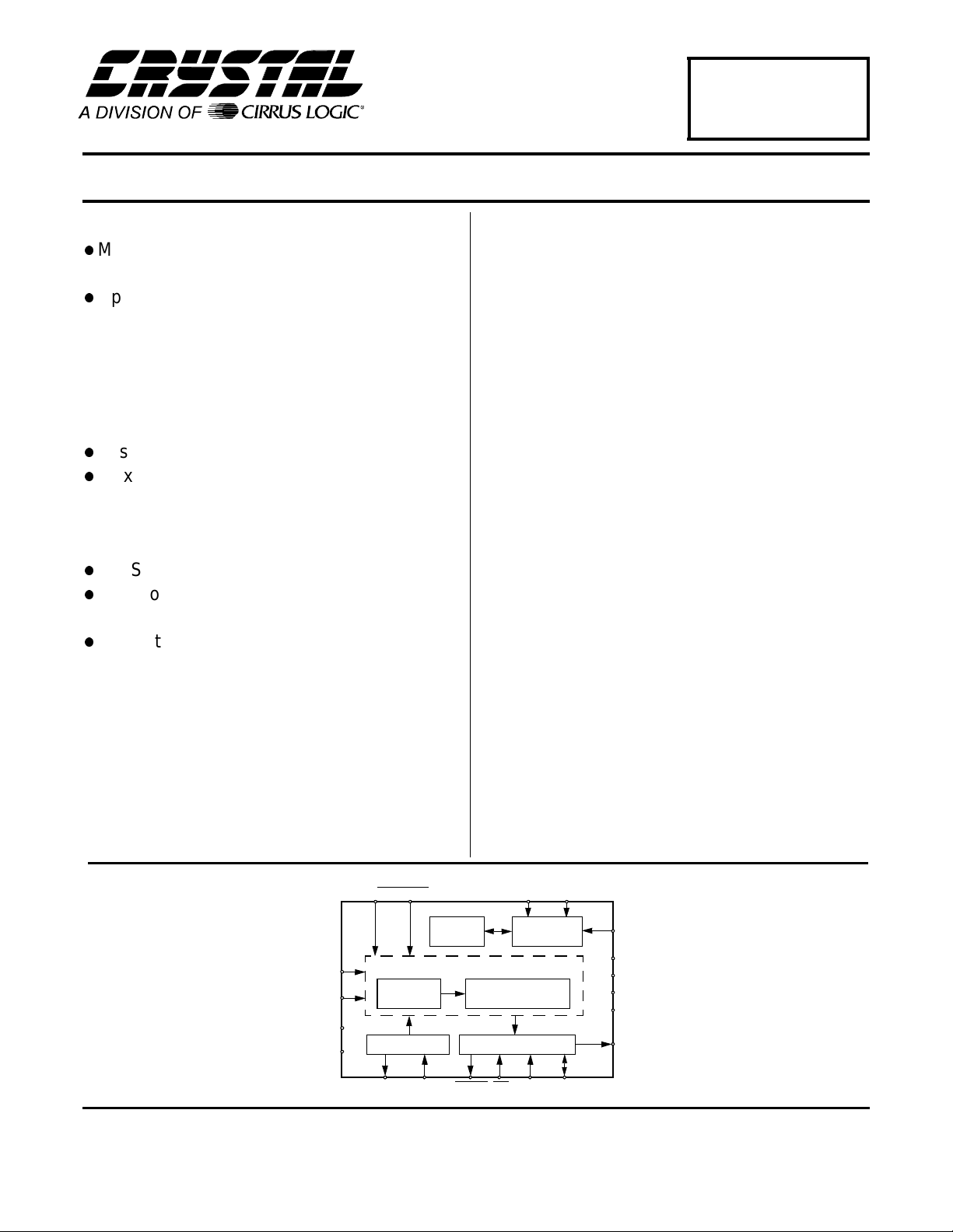
Charge-Balanced A/D Converter
Analog
Modulator
Clock Generator Serial Interface Logic
2 3 18 16 1 19
CLKOUTCLKIN DRDY CS MODESCLK
Low-Pass Digit al Filter
Copyright Cirrus Logic, I nc. 1997
SC1 SC2
Calibration
Microcontroller
6-Pole Gaussian
(All Rights Reserv ed)
13
14
15
20
7
6
CAL
VA+
VAVD+
VD-
SDATA
MAR ‘95
DS31F2
1
CS5501/CS5503
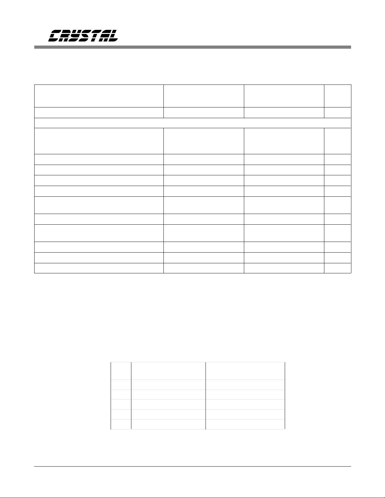
CS5501 ANALOG CHARACTERISTICS (T
VA-, VD- = -5V; VREF = 2.5V; CLKIN = 4.096MHz; Bipolar Mode; MODE = +5V; R
A
= T
MIN
to T
; VA+, VD+ = 5V;
MAX
source
= 750Ω with a 1nF
to AGND at AIN (see Note 1); Digital Inputs: Logic 0 = GND; Logic 1 = VD+; unless otherwise specified.)
CS5501-A, B, C CS5501-S, T
Parameter* Min Typ Max Min Typ Max Units
Specified Temperature Range -40 to +85 -55 to +125
°
C
Accuracy
Linearity Error -A, S
-B, T
-C
Differential Nonlinearity T
MIN
to T
MAX
Full Scale Error (Note 2) Full Scale Drift (Note 3) Unipolar Offset (Note 2) Unipolar Offset Drift (Note 3) -
-
0.0015
-
0.0007
-
0.0003
-
±
±
±
±
±
1/8
0.13
1.2
0.25
4.2
0.003
0.0015
-
-
-
0.0007
0.0012
±
1/2
±
0.5
--
±
1
-
-
-
±
1/8
±
0.13
±
2.3
±
0.25
--+3.0
0.003
0.0015
±
1/2
±
0.5
±
%FS
±
%FS
±
%FS
LSB
LSB
-LSB
±
LSB
1
-LSB
16
16
16
16
16
-25.0
Bipolar Offset (Note 2) Bipolar Offset Drift (Note 3) -
±
±
0.25
2.1
±
1
--+1.5
-
±
0.25
±
LSB
1
-LSB
16
16
-12.5
Bipolar Negative Full Scale Error (Note 2) Bipolar Negative Full Scale Drift (Note 3) -
±
0.5
±
0.6
±
2
--
-
±
0.5
±
1.2
±
LSB
2
-LSB
16
16
Noise (Referred to Output) - 1/10 - - 1/10 - LSBrms
Notes: 1. The AIN pin presents a very high input resistance at dc and a minor dynamic load which scales to the
master clock frequency. Both source resistance and shunt c apacitance are therefore critical in
determining the CS5501’s source impedance requirements. For more information refer the text section
Analog Input Impedance Considerations
.
2. Applies after calibration at the temperature of interest.
3. Total drift over the specified temperature range since calibration at power-up at 25°C (see Figure 11).
This is guaranteed by design and /or char acterization. Recalibration at any temperature will remove
these errors.
Unipolar Mode Bipolar Mode
µV LSB’s %FS ppm FS LSB’s %FS ppm FS
10 0.26 0.0004 4 0.13 0.0002 2
19 0.50 0.0008 8 0.26 0.0004 4
38 1.00 0.0015 15 0.50 0.0008 8
76 2.00 0.0030 30 1.00 0.0015 15
152 4.00 0.0061 61 2.00 0.0030 30
CS5501 Unit Conversion Factors, VREF = 2.5V
* Refer to the Specification Definitions immediately following the Pin Description Section.
2 DS31F2
CS5501/CS5503
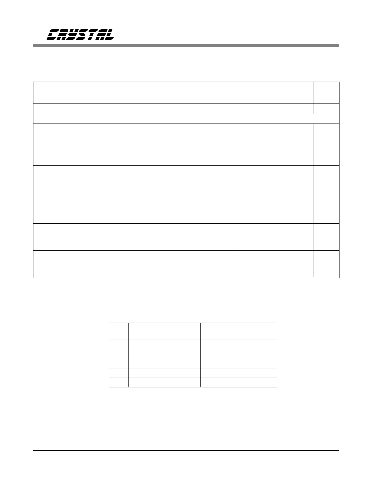
CS5503 ANALOG CHARACTERISTICS (T
VA-, VD- = -5V; VREF = 2.5V; CLKIN = 4.096MHz; Bipolar Mode; MODE = +5V; R
A
= T
MIN
to T
; VA+, VD+ = 5V;
MAX
source
= 750Ω with a 1nF
to AGND at AIN (see Note 1): unless otherwise specified.)
CS5503-A, B, C CS5503-S, T
Parameter* Min Typ Max Min Typ Max Units
Specified Temperature Range -40 to +85 -55 to +125
°
C
Accuracy
Linearity Error -A, S
-B, T
-C
Differential Nonlinearity T
MIN
to T
MAX
-
0.0015
-
0.0007
-
0.0003
0.003
0.0015
0.0012
-
-
-
0.0007
0.003
TBD
±
%FS
±
%FS
±
%FS
-20- -20-Bits
(Not Missing Codes)
Full Scale Error (Note 2) Full Scale Error Drift (Note 3) Unipolar Offset (Note 2) Unipolar Offset Drift (Note 3) -
±
4
±
19
±
4
±
67
±
16
--
±
16
--+48
-
-
±
4
±
37
±
4
±
16
±
16
LSB
-LSB
LSB
-LSB
-400
Bipolar Offset (Note 2) Bipolar Offset Drift (Note 3) -
±
4
±
34
±
16
--+24
-
±
4
±
16
LSB
-LSB
-200
Bipolar Negative Full Scale Error (Note 2) Bipolar Negative Full Scale Drift (Note 3) -
±
8
±
10
±
32
--
-
±
8
±
20
±
32-
LSB
-LSB
Noise (Referred to Output) - 1.6 - - 1.6 - LSBrms
(20)
20
20
20
20
20
20
20
20
Unipolar Mode Bipolar Mode
µ
V LSB’s %FS ppm Fs LSB’s %FS ppm FS
0.596 0.25 0.0000238 0.24 0.13 0.0000119 0.12
1.192 0.50 0.0000477 0.47 0.26 0.0000238 0.24
2.384 1.00 0.0000954 0.95 0.50 0.0000477 0.47
4.768 2.00 0.0001907 1.91 1.00 0.0000954 0.95
9.537 4.000 0.0003814 3.81 2.00 0.0001907 1.91
CS5503 Unit Conversion Factors, VREF = 2.5V
* Refer to the Specification Definitions immediately following the Pin Description Section.
DS31F2 3
CS5501/CS5503
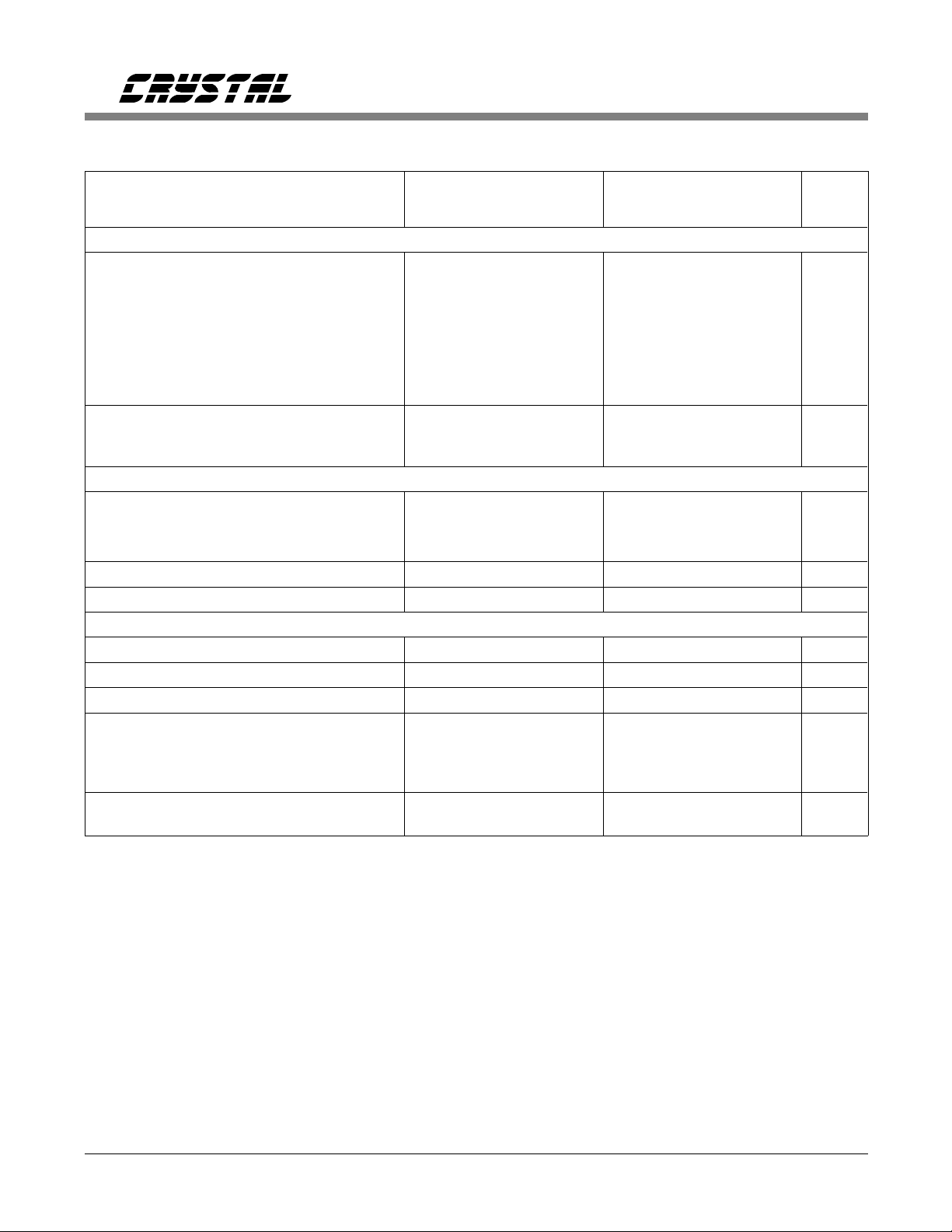
ANALOG CHARACTERISTICS (Continued)
CS5501/3-A, B, C CS5501/3-S, T
Parameter* Min Typ Max Min Typ Max Units
Power Supplies
DC Power Supply Currents
IA+
IAID+
ID- (Note 4)
Power Dissipation
SLEEP High
SLEEP Low (Note 4)
Power Supply Rejection
Positive Supplies
Negative Supplies (Note 5)
Analog Input
Analog Input Range
Unipolar
Bipolar Input Capacitance - 20 - - 20 - pF
DC Bias Current (Note 1) - 1 - - 1 - nA
System Calibration Specifications
Positive Full Scale Calibration Range VREF+0.1 VREF+0.1 V
Positive Full Scale Input Overrange VREF+0.1 VREF+0.1 V
Negative Full Scale Input Overrange -(VREF+0.1) -(VREF+0.1) V
Maximum Offset
Calibration Range (Notes 6, 7)
Unipolar Mode
Bipolar Mode
Input Span (Note 8) 80%
Notes: 4. All outputs unloaded.
5. 0.1Hz to 10Hz. PSRR at 60 Hz will exceed 120 dB due to the benefit of the digital filter.
6. In unipolar mode the offset can have a negative value (-VREF) such that the unipolar mode can mimic
bipolar mode operation.
7. The specifications for Input Overrange and for Input Span apply additional constraints on the offs et
calibration range.
8. For Unipolar mode, Input Span is the difference between full scale and zero scale. For Bipolar mode,
Input Span is the difference between positive and negative full scale points. When using less than
the maximum input span, the span range may be placed anywhere within the range of ±(VREF + 0.1).
-
-
-
-
-
-
-
-
-40%VREF to +40%VREF
VREF
2
2
1
0.03
25
10
70
75
0 to +2.5
±
2.5
-(VREF +0.1)
3.2
3.2
1.5
0.1
40
20
-
-
--
2VREF
+0.2
-
-
-
-
-
-
-
-
-40%VREF to +40%VREF
80%
VREF
2
2
1
0.03
25
10
70
75
0 to +2.5 V
±
2.5
-(VREF +0.1)
3.2
3.2
1.5
0.1
40
40
-
-
-V
2VREF
+0.2 V
mA
mA
mA
mA
mW
µ
W
dB
dB
V
V
Specifications are subject to change without notice.
4 DS31F2
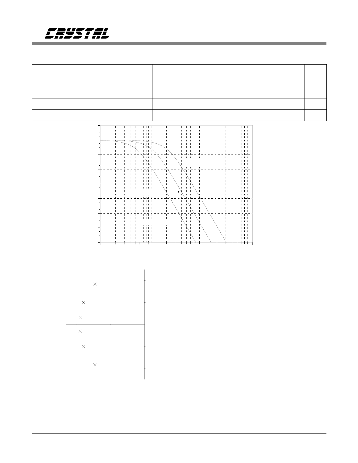
DYNAMIC CHARACTERISTICS
CS5501/CS5503
Parameter Symbol
Sampling Frequency
Output Update Rate
Filter Corner Frequency
Settling Time to +0.0007% FS (FS Step)_
20
0
-20
-40
-60
-80
Output Amplitude in dB
-100
-120
CLKIN = 2 MHz
CLKIN = 1 MHz
f
s
f
out
f
-3dB
t
s
CLKIN = 4 MHz
CLKIN/ 256
CLKIN /1024
CLKIN /409,600
506,880/CLKIN
Ratio
Units
Hz
Hz
Hz
s
-σ
-140
1 10 100
-1-2
S-Domain Pole/Zero Plot (Continuous-Time Representation)
H(x) = [1 + 0.694x
where x = f /f
Continuous-Time Representation of 6-Pole Gaussian Filter
Frequency in Hz
1000
Frequency Response
jω
j2
j1
-j1
-j2
2
+ 0.241x4 + 0.0557x6 + 0.009664x8 + 0.00134x10 + 0.000155x12]
-3dB
, f
= CLKIN/409,600 , and f is the frequency of inter est.
-3dB
S
= -1.4667 ± j1.8199
1,2
S
= -1.7559 ± j1.0008
3,4
S
= -1.8746 ± j0.32276
5,6
-1/2
DS31F2 5
CS5501/CS5503
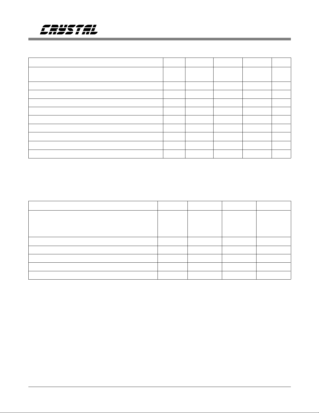
DIGITAL CHARACTERISTICS
(TA = T
min
to T
Parameter Symbol Min Typ Max Units
Calibration Memory Retention
Power Supply Voltage (VD+ and VA+)
High-Level Input Voltage All Except CLKIN V
High-Level Input Voltage CLKIN V
Low-Level Input Voltage All Except CLKIN V
Low-Level Input Voltage CLKIN V
High-Level Output Voltage (Note 9) V
Low-Level Output Voltage Iout=1.6mA V
Input Leakage Current I
3-State Leakage Current I
Digital Output Pin Capacitance C
Notes: 9. I
= -100 µA. This guarantees the ability to drive one TTL load. (VOH = 2.4V @ I
out
ABSOLUTE MAXIMUM RATINGS
Parameter Symbol Min Max Units
; VA+, VD+ = 5V ± 10%; VA-, VD- = -5V ± 10%)
max
V
MR
IH
IH
IL
IL
OH
OL
in
OZ
out
2.0 - - V
2.0 - - V
3.5 - - V
--0.8V
--1.5V
(VD+)-1.0V - - V
--0.4V
--10
--
±10µ
-9-pF
= -40 µA).
out
µ
A
A
DC Power Supplies: Positive Digital
Negative Digital
Positive Analog
Negative Analog
Input Current, Any Pin Except Supplies (Notes 10, 11) I
Analog Input Voltage (AIN and VREF pins) V
Digital Input Voltage V
Ambient Operating Temperature T
Storage Temperature T
VD+
VD-
VA+
VA-
in
INA
IND
A
stg
-0.3
0.3
-0.3
0.3
-
(VA+)+0.3
-6.0
6.0
-6.0
±
10
(VA-)-0.3 (VA+)+0.3 V
-0.3 (VA+)+0.3 V
-55 125 C°
-65 150 C°
Notes: 10. Applies to all pins including continuous overvoltage conditions at the analog input (AIN) pin.
11. Transient currents of up to 100mA will not cause SCR latch-up. Maximum input current for a power
supply pin is ± 50 mA.
V
V
V
V
mA
6 DS31F2
CS5501/CS5503
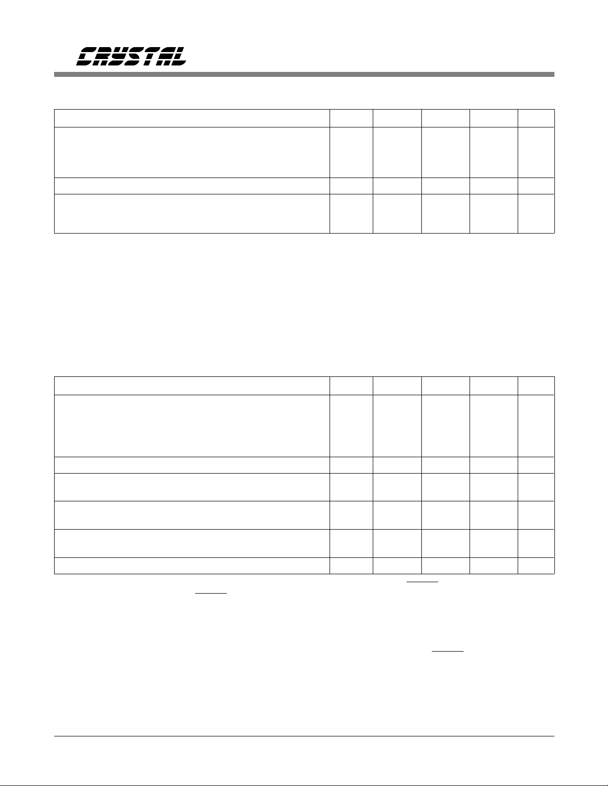
RECOMMENDED OPERATING CONDITIONS (AGND, DGND = 0V) (Note 12)
Parameter Symbol Min Typ Max Units
DC Power Supplies: Positive Digital
Negative Digital
Positive Analog
Negative Analog
VD+
VD-
VA+
VA-
4.5
-4.5
4.5
-4.5
5.0
-5.0
5.0
-5.0
VA+
-5.5
5.5
-5.5
Analog Reference Voltage VREF 1.0 2.5 3.0 V
Analog Input Voltage: (Note 13)
Unipolar
Bipolar
V
AIN
V
AIN
AGND
-VREF
-
-
VREF
VREF
Notes: 12. All voltages with respect to ground.
13. The CS5501 and CS5503 can accept input voltages up to the analog supplies (VA+ and VA-). They
will accurately convert and filter signals with noise excursions up to 100mV beyond |VREF|.
After filtering, the devices will output all 1’s for any input above VREF and all 0’s for any input below
AGND in unipolar mode and -VREF in bipolar mode.
SWITCHING CHARACTERISTICS
VA-, VD- = -5V ± 10%; Input Levels: Logic 0 = 0V, Logic 1 = VD+; C
(TA = T
min
to T
; CLKIN=4.096 MHz; VA+, VD+ = 5V±10%;
max
= 50 pF; unless otherwise specified.)
L
Parameter Symbol Min Typ Max Units
Master Clock Frequency: Internal Gate Oscillator
CLKIN
200
4096
5000
(See Table 1)
Externally Supplied: (Note 14)
Maximum
Minimum (Note 15)
CLKIN
CLKIN
-
200
40
-
5000
CLKIN Duty Cycle 20 - 80 %
Rise Times: Any Digital Input
Any Digital Output (Note 16)
Fall Times: Any Digital Input
Any Digital Output (Note 16)
Set Up Times: SC1, SC2 to CAL Low
SLEEP High to CLKIN High (Note 17)
Hold Time: SC1, SC2 hold after CAL falls t
t
rise
t
rise
t
t
t
scs
t
sch
fall
fall
sls
-
-
-
-
100
1
100 - - ns
20
20
-
1.0
-
-
1.0
-
-
-
-
-
V
V
V
V
V
V
kHz
kHz
kHz
µ
s
ns
µ
s
ns
ns
µ
s
Notes: 14. CLKIN must be supplied whenever the CS5501 or CS5503 is not in SLEEP mode. If no clock is
present when not in
SLEEP mode, the device can draw higher current than specified
and possibly become uncalibrated.
15. The CS5501/CS5503 is production tested at 4.096 MHz. It is guaranteed by characterization
to operate at 200 kHz.
16. Specified using 10% and 90% points on waveform of interest.
17. In order to synchronize several CS5501’s or CS5503’s together using the
SLEEP pin,
this specification must be met.
DS31F2 7
CS5501/CS5503
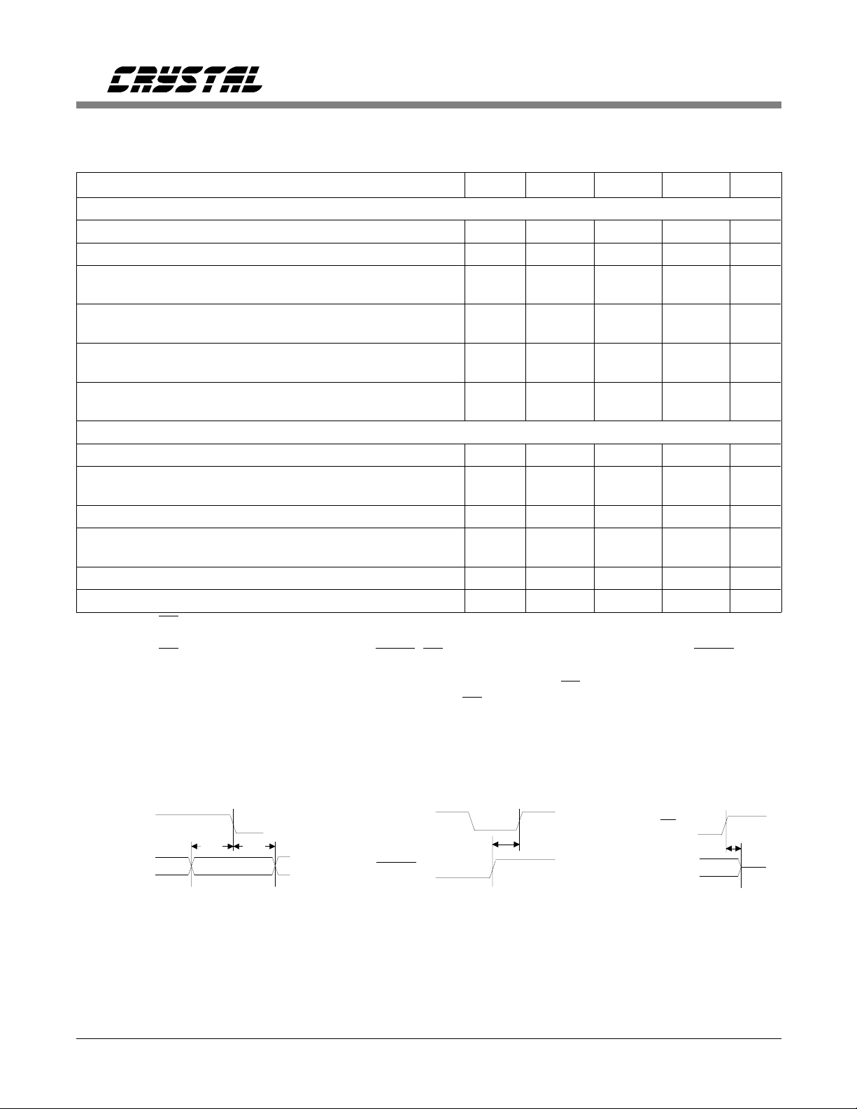
SWITCHING CHARACTERISTICS
(continued) (TA = T
VA-, VD- = -5V ± 10%; Input Levels: Logic 0 = 0V, Logic 1 = VD+; C
Parameter Symbol Min Typ Max Units
SSC Mode (Mode = VD+)
Access Time CS Low to SDATA Out t
SDATA Delay Time SCLK Falling to New SDATA bit t
SCLK Delay Time SDATA MSB bit to SCLK Rising
csd1
dd1
t
cd1
(at 4.096 MHz)
Serial Clock Pulse Width High (at 4.096 MHz)
(Out) Pulse Width Low
Output Float Delay SCLK Rising to Hi-Z t
Output Float Delay CS High to Output Hi-Z (Note 18) t
t
ph1
t
pl1
fd2
fd1
SEC Mode (Mode = DGND)
Serial Clock (In) f
Serial Clock (In) Pulse Width High
Pulse Width Low
Access Time CS Low to Data Valid (Note 19) t
sclk
t
ph2
t
pl2
csd2
Maximum Data Delay Time (Note 20)
SCLK Falling to New SDATA bit t
Output Float Delay CS High to Output Hi-Z t
Output Float Delay SCLK Falling to Output Hi-Z t
Notes: 18. If
CS is returned high before all data bits ar e output, the SDATA and S CLK outputs will complete
dd2
fd3
fd4
the current data bit and then go to high impedance.
CS is activated asynchronously to DRDY, CS will not be recognized if it occurs when DRDY is high
19. If
for 4 clock cycles. The propagation delay time may be as great as 4 CLKIN cycles plus 160 ns.
To guarantee proper clocking of SDATA when using asychronous
high sooner than 4 CLKIN cycles plus 160ns after
CS goes low.
20. SDATA transitions on the falling edge of SCLK(i).
to T
min
= 50 pF)
L
; VA+, VD+ = 5V ± 10%;
max
3/CLKIN - - ns
- 25 100 ns
250 380 - ns
-
-
- 1/CLKIN
240
730
+ 100
300
790
1/CLKIN
+ 200
--4/CLKIN
+200
dc - 4.2 MHz
50
180
-
-
-
-
- 80 160 ns
- 75 150 ns
- - 250 ns
- 100 200 ns
CS, SCLK(i) should not be taken
ns
ns
ns
ns
CAL
scstsch
SC1, SC2
Calibration Control Timing
t
VALID
CLKIN
SLEEP
Sleep Mode Timing for
Synchronization
CS
t
sls
SDATA
t
fd1
Output Float Delay
SSC Mode (Note 19)
8 DS31F2
CLKIN
CS
SDATA
SCLK (o)
t
csd1
Hi-Z Hi-ZMSB-2 LSBMSB MSB-1
t
dd1
t
cd1
Hi-Z
t
ph1
t
pl1
SSC MODE Timing Relationships
CS5501/CS5503
t
fd2
Hi-Z
DRDY
CS
SDATA
SCLK (i)
CS
SDATA
SCLK (i)
t
csd2
Hi-Z MSB MSB-1
t
t
dd2
dd2
t
ph2
t
csd2
Hi-Z Hi-ZLSBMSB MSB-1
t
dd2
t
ph2
SEC MODE Timing Relationships
t
fd4
t
t
pl2
fd3
Hi-Z
DS31F2 9
CS5501/CS5503
SWITCHING CHARACTERISTICS (continued) (T
A
= T
min
to T
max
;
VA+, VD+ = 5V ± 10%; VA-, VD- = -5V ± 10%; Input Levels: Logic 0 = 0V, Logic 1 = VD+; C
Parameter Symbol Min Typ Max Units
AC Mode (Mode = VD-) CS5501 only
Serial Clock (In) f
Serial Clock (In) Pulse Width High
Pulse Width Low
Set-up Time CS Low to SCLK Falling t
Maximum Data Delay Time SCLK Fall to New SD ATA bit t
Output Float Delay CS High to Output Hi-Z (Note 21) t
Notes: 21. If
CS is returned high after an 11-bit data pac ket is started, the SDATA output will continue to output
sclk
t
ph3
t
pl3
css
dd3
fd5
dc - 4.2 MHz
50
180
-
-
-2040ns
- 90 180 ns
- 100 200 ns
data until the end of the second stop bit. At that time the SDATA output will go to high impedance.
= 50 pF)
L
-
-
ns
ns
DRDY
CS
SCLK(i)
SDATA
t
css
t
dd3
Hi-Z Hi-ZBIT7BIT6BIT9
START
BIT8
High Byte
t
AC MODE Timing Relationships (CS5501 only)
t
ph3
pl3
Low Byte
STOP1
STOP2
t
fd5
10 DS31F2
CS5501/CS5503
GENERAL DESCRIPTION
The CS5501/CS5503 are monolithic CMOS A/D
converters designed specifically for high resolution measurement of low-frequency signals. Each
device consists of a charge-balance converter (16Bit for the CS5501, 20-Bit for the CS5503),
calibration microcontroller with on-chip SRAM,
and serial communications port.
The CS5501/CS5503 A/D converters perform
conversions continuously and update their output
ports after every conversion (unless the serial port
is active). Conversions are performed and the serial port is updated independent of external
control. Both devices are capable of measuring
either unipolar or bipolar input signals, and calibration cycles may be initiated at any time to
ensure measurement accuracy.
The CS5501/CS5503 perform conversions at a
rate determined by the master clock signal. The
master clock can be set by an external clock or
with a crystal connected to the pins of the on-chip
gate oscillator. The master clock frequency determines:
1. The sample rate of the analog input signal.
2. The corner frequency of the on-chip digital
filter.
3. The output update rate of the serial output port.
The CS5501/CS5503 design includes several selfcalibration modes and several serial port interface
modes to offer users maximum system design
flexiblity.
The Delta-Sigma Conversion Method
The CS5501/CS5503 A/D converters use chargebalance techniques to achieve low cost, high
resolution measurements. A charge-balance A/D
converter consists of two basic blocks: an analog
modulator and a digital filter. An elementary example of a charge-balance A/D converter is a
conventional voltage-to-frequency converter and
counter. The VFC’s 1-bit output conveys infor-
mation in the form of frequency (or duty cycle),
which is then filtered (averaged) by the counter
for higher resolution.
LP Filter
S/H Amp
Figure 1. Charge Balance (Delta-Sigma) A/D Converter
Comparator
DAC
1-bit
Digital Filter
16-bits
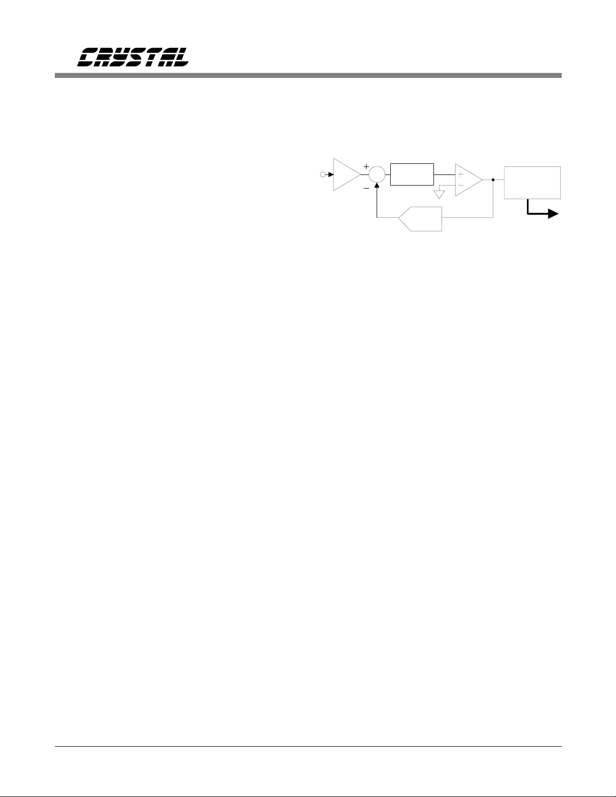
The analog modulator of the CS5501/CS5503 is a
multi-order delta-sigma modulator. The modulator
consists of a 1-bit A/D converter (that is, a comparator) embedded in an analog feedback loop
with high open loop gain (see Figure 1). The
modulator samples and converts the input at a rate
well above the bandwidth of interest. The 1-bit
output of the comparator is sampled at intervals
based on the clock rate of the part and this information (either a 1 or 0) is conveyed to the digital
filter. The digital filter is much more sophisticated
than a simple counter. The filter on the chip has a
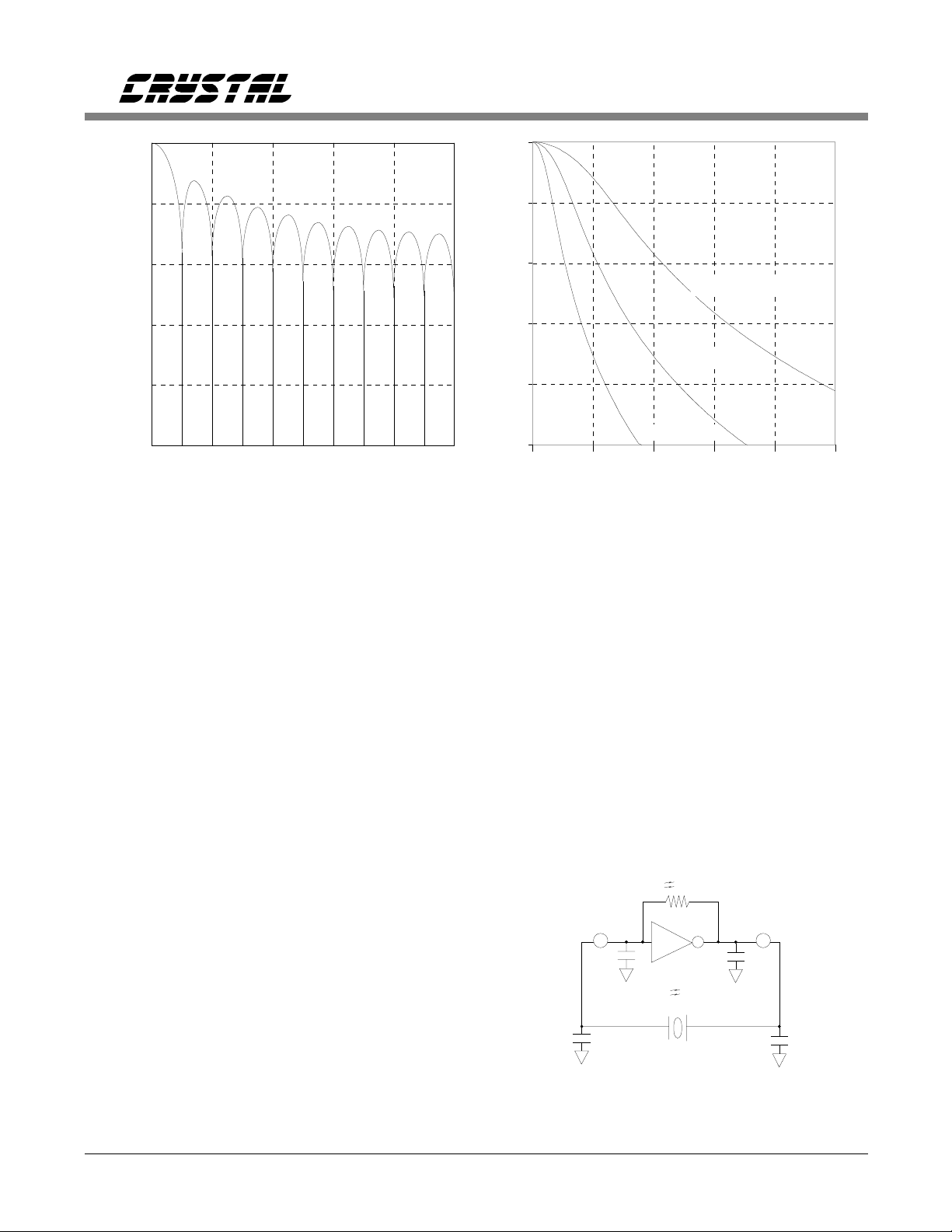
6-pole low pass Gaussian response which rolls off
at 120 dB/decade (36 dB/octave). The corner frequency of the digital filter scales with the master
clock frequency. In comparison, VFC’s and dual
slope converters offer (sin x)/x filtering for high
frequency rejection (see Figure 2 for a comparison of the characteristics of these two filter types).
When operating from a 1 MHz master clock the
digital filter in the CS5501/CS5503 offers better
than 120 dB rejection of 50 and 60 Hz line frequencies and does not require any type of line
synchronization to achieve this rejection. It should
be noted that the CS5501/CS5503 will update its
output port almost at 1000 times per second when
operating from the 1 MHz clock. This is a much
higher update rate (typically by a factor of at least
50 times) than either VFCs or dual-slope converters can offer.
For a more detailed discussion on the delta-sigma
modulator see the Application note "Delta-Sigma
DS31F2 11
CS5501/CS5503
Magnitude (dB)
-100
-20
-40
-60
-80
0
0
20
40 60 80 100
Frequency (Hz)
0
-20
-40
-60
Magnitude (dB)
-80
-100
CLKIN = 4 MHz
CLKIN = 2 MHz
CLKIN=1 MHz
0
20 40 60 80 10 0
Frequency (Hz)
a. Averaging (Integrating) Filter Response (tavg = 100 ms) b. 6-Pole Gaussian Filter Response
Figure 2. Filter Responses
A/D Conversion Technique Overview" in the ap-
Clock Generator
plication note section of the data book. The
application note discusses the delta-sigma modulator and some aspects of digital filtering.
The CS5501/CS5503 both include gates which
can be connected as a crystal oscillator to provide
the master clock signal for the chip. Alternatively,
an external (CMOS compatible) clock can be in-
OVERVIEW
put to the CLKIN pin as the master clock for the
device. Figure 3 illustrates a simple model of the
As shown in the block diagram on the front page
of the data sheet, the CS5501/CS5503 can be segmented into five circuit functions. The heart of the
chip is the charge balance A/D converter (16-bit
for the CS5501, 20-bit for the CS5503). The con-
on-chip gate oscillator. The gate has a typical
transconductance of 1500 µmho. The gate model
includes 10 pf capacitors at the input and output
pins. These capacitances include the typical stray
capacitance of the pins of the device. The on-chip
verter and all of the other circuit functions on the
500 k
chip must be driven by a clock signal from the
R
1
clock generator. The serial interface logic outputs
the converted data. The calibration microcontroller along with the calibration SRAM (static
RAM), supervises the device calibration. Each
segment of the chip has control lines associated
CLKIN CLKOUT
3
10pF
g
1500 umho
m
with it. The function of each of the pins is described in the pin description section of the data
sheet.
C1 * Y1 C2 *
* See Table 1
Ω
2
10pF
Figure 3. On-chip Gate Oscillator Model
12 DS31F2
CS5501/CS5503
gate oscillator is designed to properly operate
without additional loading capacitors when using
a 4.096 MHz (or 4 MHz) crystal. If other crystal
frequencies or if ceramic resonators are used,
loading capacitors may be necessary for reliable
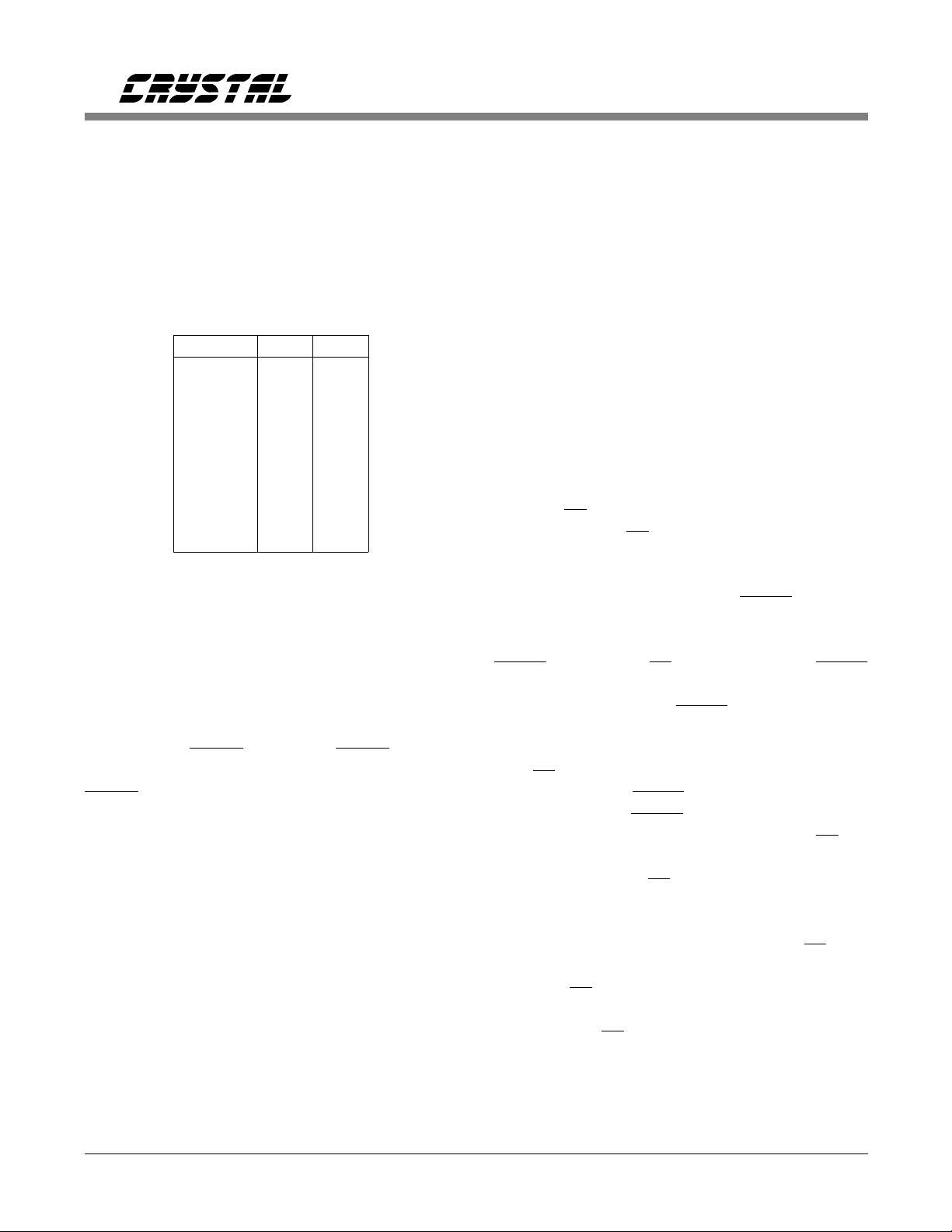
operation of the oscillator. Table 1 illustrates some
typical capacitor values to be used with selected
resonating elements.
C1 C2Resonators
Ceramic
330pF 470pF200 kHz
100pF 100pF455 kHz
50pF 50pF1.0 MHz
20pF 20pF2.0 MHz
Crystals
30pF 30pF2.000 MHz
20pF 20pF3.579 MHz
None None4.096 MHz
Table 1. Resonator Loading Capacitors
CLKOUT (pin 2) can be used to drive one external CMOS gate for system clock requirements. In
this case, the external gate capacitance must be
taken into account when choosing the value of
C2.
Caution: A clock signal should always be present
whenever the SLEEP is inactive (SLEEP = VD+).
If no clock is provided to the part when not in
SLEEP, the part may draw excess current and
possibly even lose its calibration data. This is because the device is built using dynamic logic.
Serial Interface Logic
The CS5501 serial data output can operate in any
one of the following three different serial interface
modes depending upon the MODE pin selection:
SSC (Synchronous Self-Clocking) mode;
MODE pin tied to VD+ (+5V).
SEC (Synchronous External Clocking) mode;
MODE pin tied to DGND.
and AC (Asynchronous Communication) mode;
CS5501 only
MODE pin tied to VD- (-5V)
The CS5503 can only operate in the first two
modes, SEC and SSC.
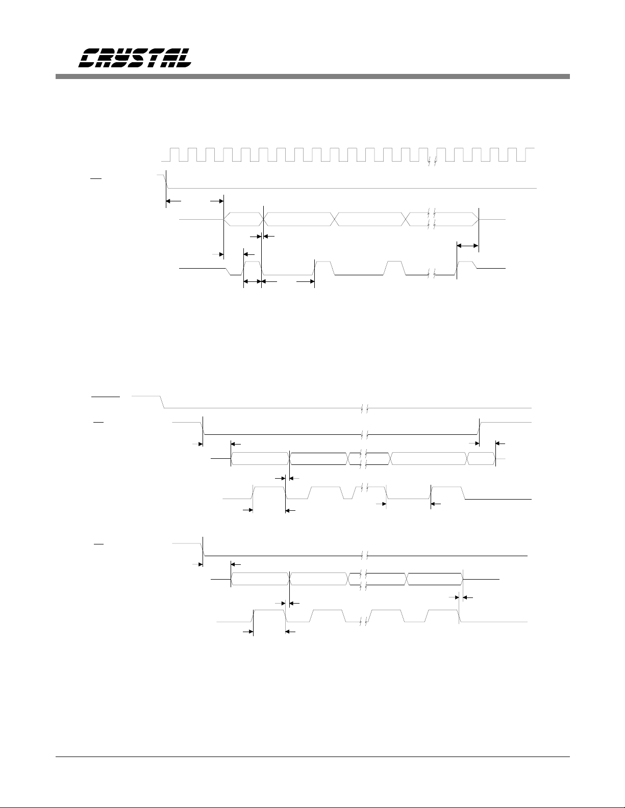
Synchronous Self-Clocking Mode
When operated in the SSC mode (MODE pin tied
to VD+), the CS5501/CS5503 furnish both serial
output data (SDATA) and an internally-generated
serial clock (SCLK). Internal timing for the SSC
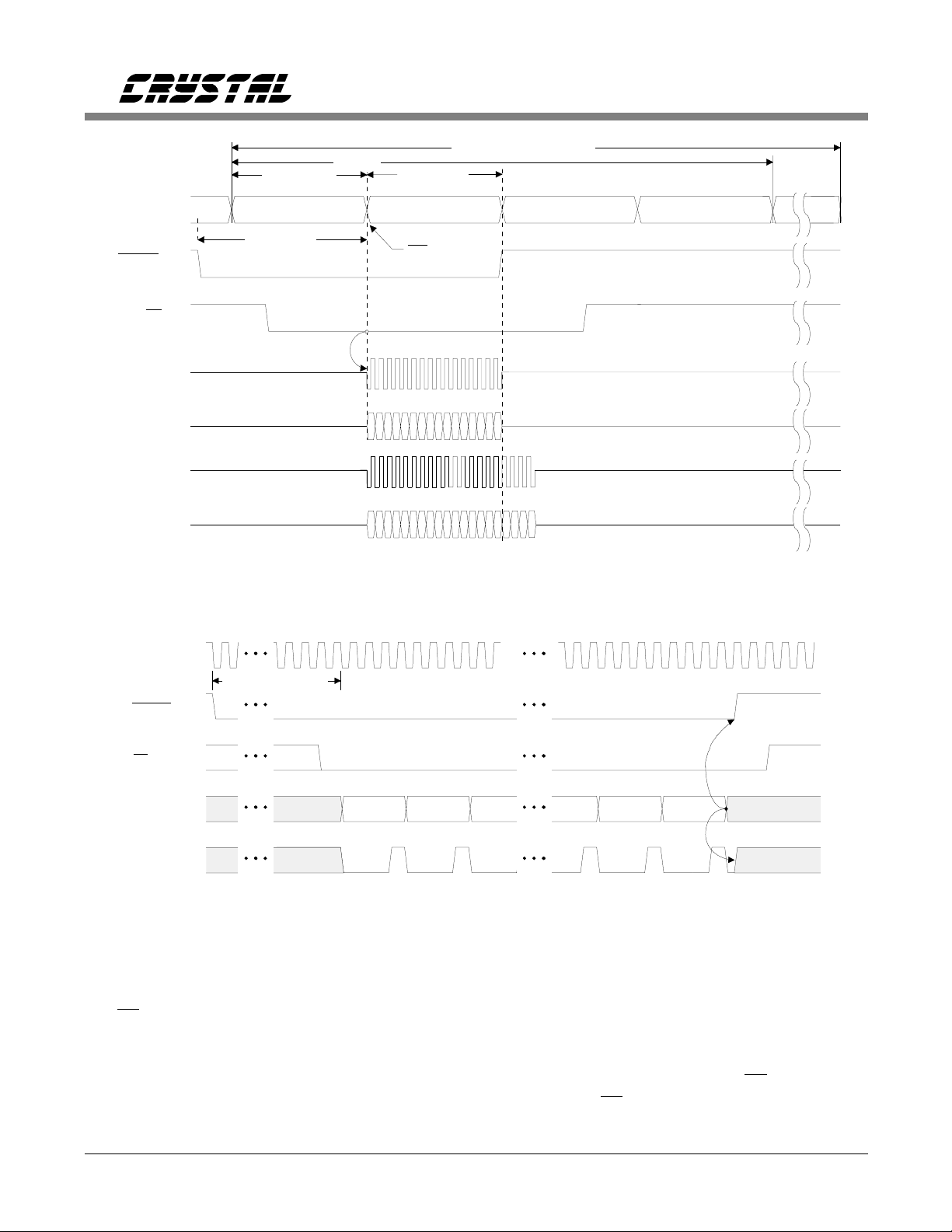
mode is illustrated in Figure 4. Figure 5 shows
detailed SSC mode timing for both the
CS5501/CS5503. A filter cycle occurs every 1024
cycles of CLKIN. During each filter cycle, the
status of CS is polled at eight specific times dur-
ing the cycle. If CS is low when it is polled, the
CS5501/CS5503 begin clocking the data bits out,
MSB first, at a SCLK output rate of CLKIN/4.
Once transmission is complete, DRDY rises and
both SDATA and SCLK outputs go into a high
impedance state. A filter cycle begins each time
DRDY falls. If the CS line is not active, DRDY
will return high 1020 clock cycles after it falls.
Four clock cycles later DRDY will fall to signal
that the serial port has been updated with new
data and that a new filter cycle has begun. The
first CS polling during a filter cycle occurs 76
clock cycles after DRDY falls (the rising edge of
CLKIN on which DRDY falls is considered clock
cycle number one). Subsequent pollings of CS oc-
cur at intervals of 128 clock cycles thereafter (76,
204, 332, etc.). The CS signal is polled at the be-
ginning of each of eight data output windows
which occur in a filter cycle. To transmit data dur-
ing any one of the eight output windows, CS must
be low at least three CLKIN cycles before it is
polled. If CS does not meet this set-up time, data
will not be transmitted during the window time.
Furthermore, CS is not latched internally and
therefore must be held low during the entire data
transmission to obtain all of the data bits.
DS31F2 13
Internal
Status
64/CLKIN
Note 1
Analog Time 0 Digital Time 0
64/CLKIN
f
=1024/CLKIN
out
Analog Time 1 Digital Time1
CS5501/CS5503
76/CLKIN
DRDY (o)
CS (i)
CS5501
SCLK (o)
CS5501
SDATA (o)
CS5503
SCLK (o)
CS5503
SDATA (o)
Note: 1. There are 16 analog and digital settling periods per filter cycle (4 are s hown). Data can be output in the
SSC mode in only 1 of the 8 digital time periods in each filter cycle.
CLKIN (i )
Hi-Z
Hi-Z
Hi-Z
Hi-Z
76 CLKIN cycles
CS Polled
(MSB)
(MSB) (LSB)
Figure 4. Internal Timing
(LSB)
Hi-Z
Hi-Z
Hi-Z
Hi-Z
DRDY (o)
CS (i)
(MSB) (LSB)
SDATA (o)
SCLK (o)
*
CS5501
**
CS5503
Hi-Z B0B1 Hi-Z
Figure 5. Synchronous Self-Clocking (SSC) Mode Timing
B15*
B19**
The eighth output window time overlaps the time
in which the serial output port is to be updated. If
B14*
B18**
Hi-ZHi-Z
(CLKIN = 4.096 MHz) instead of the normal
4 kHz serial port update rate.
the CS is recognized as being low when it is
polled for the eighth window time, data will be
output as normal, but the serial port will not be
updated with new data until the next serial port
update time. Under these conditions, the serial
port will experience an update rate of only 2 kHz
14 DS31F2
Upon completion of transmission of all the data
bits, the SCLK and SDATA outputs will go to a
high impedance state even with CS held low. In
the event that CS is taken high before all data bits
are output, the SDATA and SCLK outputs will
CS5501/CS5503
complete the current data bit output and go to a
high impedance state when SCLK goes low.
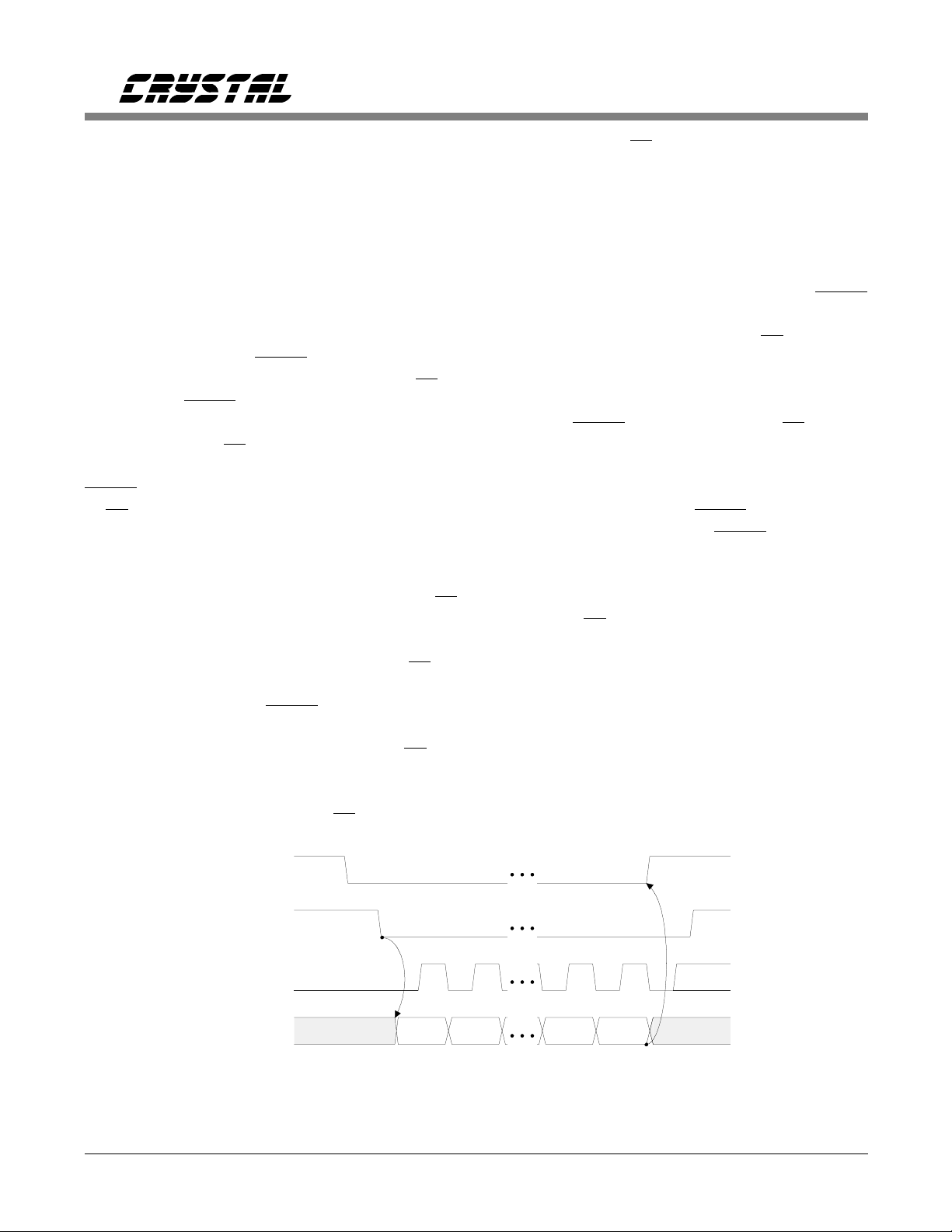
Synchronous External Clocking Mode
When operated in the SEC mode (MODE pin tied
to DGND), the CS5501/CS5503 outputs the data
in its serial port at a rate determined by an external clock which is input into the SCLK pin. In
this mode the output port will be updated every
1024 CLKIN cycles. DRDY will go low when
new data is loaded into the output port. If CS is
not active, DRDY will return positive 1020
CLKIN cycles later and remain so for four
CLKIN cycles. If CS is taken low it will be recognized immediately unless it occurs while
DRDY is high for the four clock cycles. As soon
as CS is recognized, the SDATA output will come
out of its high-impedance state and present the
MSB data bit. The MSB data bit will remain present until a falling edge of SCLK occurs to
advance the output to the MSB-1 bit. If the CS
and external SCLK are operated asynchronously
to CLKIN, errors can result in the output data unless certain precautions are taken. If CS is
activated asynchronously, it may occur during the
four clock cycles when DRDY is high and therefore not be recognized immediately. To be certain
that data misread errors will not result if CS occurs at this time, the SCLK input should not
transition high to latch the MSB until four
CLKIN cycles plus 160 ns after CS is taken low.
This insures that CS will be recognized and the
MSB bit will become stable before the SCLK
transitions p ositive t o latch the M SB data bit.
When SCLK returns low the serial port will pre-
sent the MSB-1 data bit on its output.
Subsequent cycles of SCLK will advance the data
output. When all data bits are clocked out, DRDY
will then go high and the SDATA output will go
into a high impedance state. If the CS input goes
low and all of the data bits are not clocked out of
the port, filter cycles will continue to occur but
the output serial port will not be updated with
new data (DRDY will remain low). If CS is taken
high at any time, the SDATA output pin will go to
a high impedance state. If any of the data bits in
the serial port have not been clocked out, they
will remain available until DRDY returns high for
four clock cycles. After this DRDY will fall and
the port will be updated with a new 16-bit word
in the CS5501 or 20-bit word in the CS5503. It
is acceptable to clock out less than all possible
data bits if CS is returned high to allow the port
to be updated. Figure 6 illustrates the serial port
timing in the SEC mode.
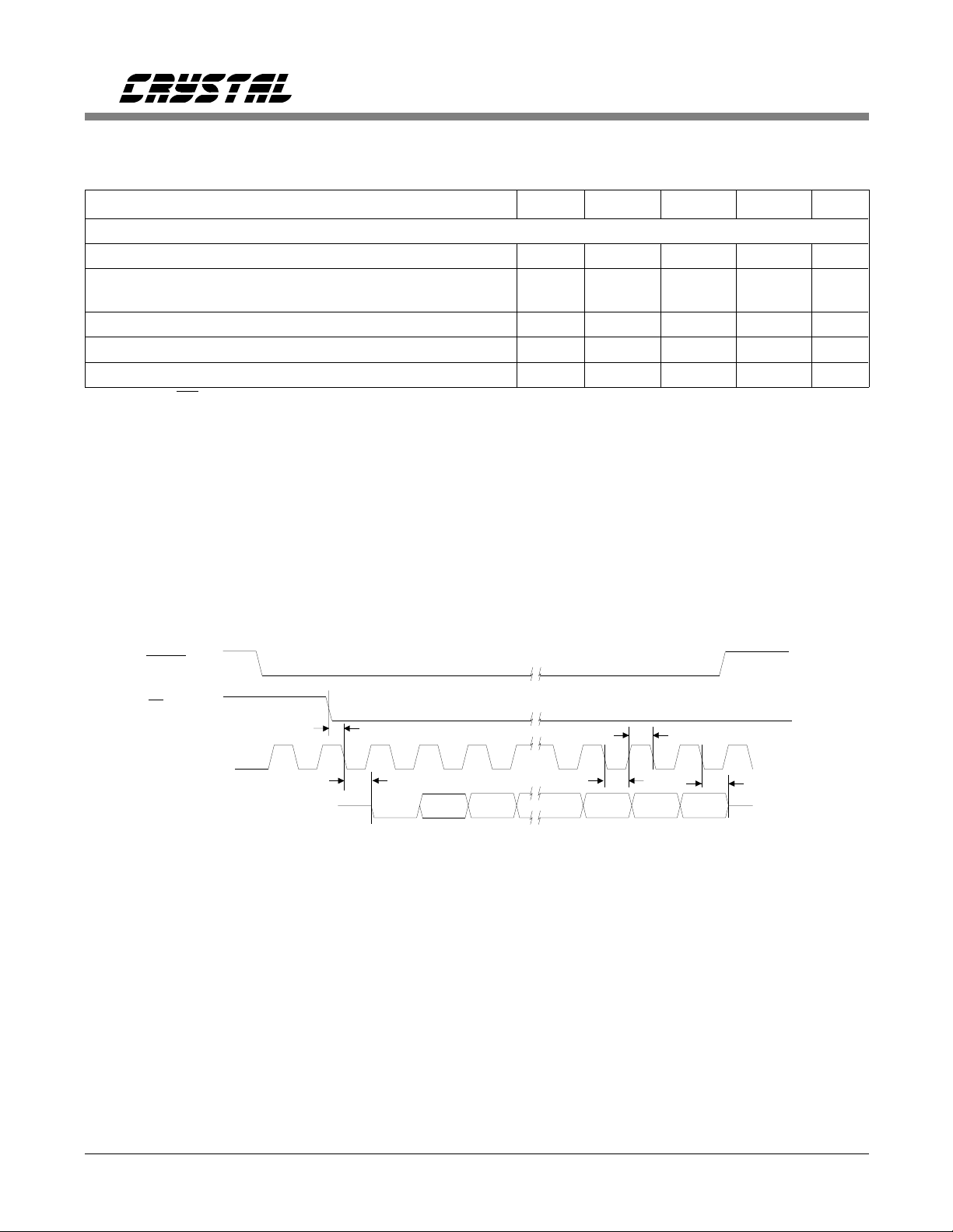
Asynchronous Communication Mode (CS5501
Only)
In the CS5501, the AC mode is activated when
the MODE pin is tied to VD- (-5 V). When oper-
ating in the AC mode the CS5501 is designed to
DRDY (o)
CS (i)
SCLK (i)
(MSB)
SDATA (o)
DS31F2 15
Hi-Z
CS5501
*
**
CS5503
Figure 6. Synchronous External-Clocking (SEC) Mode Timing
B15* B14*
B19** B18**
(LSB)
B0B1
Hi-Z
CS5501/CS5503
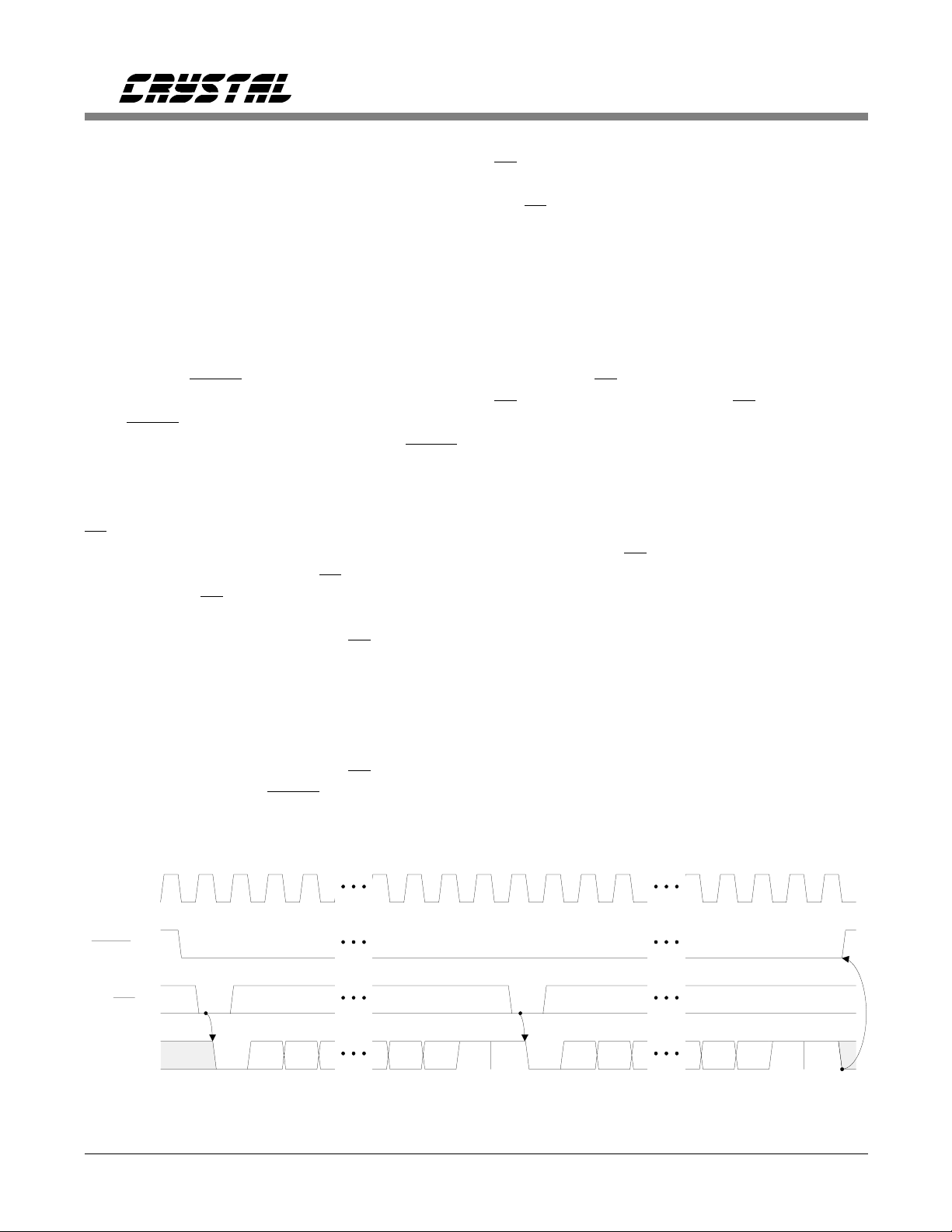
provide data output in UART compatible format.
The baud rate of the SDATA output will be determined by the rate of the SCLK input. The data
which is output of the SDATA pin will be formatted such that it will contain two 11 bit data
packets. Each packet includes one start bit, eight
data bits, and two stop bits. The packet which carries the most-significant-byte data will be output
first, with its lsb being the first data bit output
after the start bit.
In this mode, DRDY will occur every 1024 clock
cycles. If the serial port is not outputting a data
byte, DRDY will return high after 1020 clock cycles and remain high for 4 clock cycles. DRDY
will then go low to indicate that an update to the
serial output port with a new 16 bit word has occurred. To initiate a transmission from the port the
CS line must be taken low. Then SCLK, which is
an input in this mode, must transition from a high
to a low to latch the state of CS internal to the
CS5501. Once CS is recognized and latched as a
low, the port will begin to output data. Figure 7
details the timing for this output. CS can be returned high before the end of the 11-bit
transmission and the transmission will continue
until the second stop bit of the first 11-bit packet
is output. The SDATA output will go into a high
impedance state after the second stop bit is output.
To obtain the second 11-bit packet CS must again
be brought low before DRDY goes high or the
second 11-bit data packet will be overwritten with
a serial port update. For the second 11-bit packet,
CS need only to go low for 50 ns; it need not be
latched by a falling edge of SCLK. Alternately,
the CS line can be taken low and held low until
both 11-bit data packets are output. This is the
preferred method of control as it will prevent los-
ing the second 11-bit data packet if the port is
updated. Some serial data rates can be quite slow
compared to the rate at which the CS5501 can up-
date its output port. A slow data rate will leave
only a short period of time to start the second 11-
bit packet if CS is returned high momentarily. If
CS is held low continuously (CS hard-wired to
DGND), the serial port will be updated only after
all 22 bits have been clocked out of the port.
Upon the completion of a transmission of the two
11-bit data packets the SDATA output will go into
a high impedance state. If at any time during
transmission the CS is taken back high, the cur-
rent 11-bit data packet will continue to be output.
At the end of the second stop bit of the data
packet, the SDATA output will go into a high im-
pedance state.
Linearity Performance
The CS5501/CS5503 delta-sigma converters are
like conventional charge-balance converters in
that they have no source of nonmonotonicity. The
devices therefore have no missing codes in their
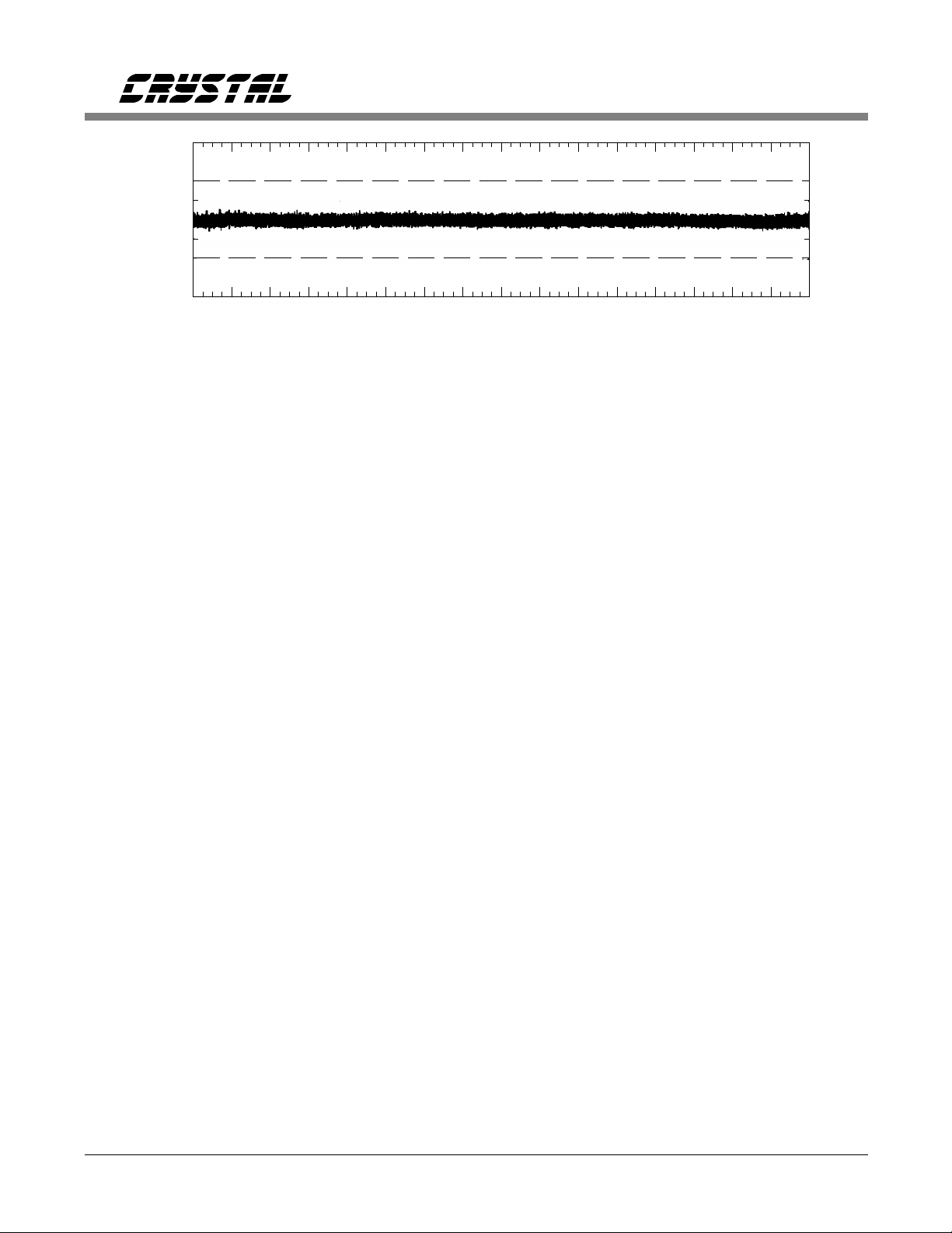
transfer functions. See Figure 8 for a plot of the
SCLK (i)
DRDY (o)
CS (i)
Stop
SDATA (o)
16 DS31F2
Hi-Z Start B8 B9 B14 B15 Start B0 B1 B6 B7
Figure 7. CS5501 Asynchronous (UART) Mode Timing
Stop
12
StopStop
12
CS5501/CS5503
+1
+1/2
0
DNL (LSB)
-1/2
-1
0 65,535
Figure 8. CS5501 Differential Nonlinearity Plot
32,768
Codes
excellent differential linearity achieved by the
CS5501. The CS5501/CS5503 also have excellent
integral linearity, which is accomplished with a
well-designed charge-balance architecture. Each
device also achieves low input drift through the
use of chopper-stabilized techniques in its input
stage. To assure that the CS5501/CS5503 achieves
excellent performance over time and temperature,
it uses digital calibration techniques to minimize
offset and gain errors to typically within ±1/2
LSB at 16 bits in the CS5501 and ±4 LSB at 20
bits in the CS5503.
Converter Calibration
The CS5501/CS5503 offer both self-calibration
and system level calibration capability. To understand the calibration features, a basic
comprehension of the internal workings of the
converter are helpful. As mentioned previously in
this data sheet, the converter consists of two sections. First is the analog modulator which is a
delta-sigma type charge-balance converter. This
is followed by a digital filter. The filter circuitry
is actually an arithmetic logic unit (ALU) whose
architecture and instructions execute the filter
function. The modulator (explained in more detail in the applications note "Delta-Sigma
Conversion Technique Overview") uses the VREF
voltage connected to pin 10 to determine the magnitude of the voltages used in its feedback DAC.
The modulator accepts an analog signal at its in-
put and produces a data stream of 1’s and 0’s as
its output. This data stream value can change
(from 1 to 0 or vice versa) every 256 CLKIN cycles. As the input voltage increases the ratio of
1’s to 0’s out of the modulator increases proportionally. The 1’s density of the data stream out of
the modulator therefore provides a digital representation of the analog input signal where the 1’s
density is defined as the ratio of the number of 1’s
to the number of 0’s out of the modulator for a
given period of time. The 1’s density output of the
modulator is also a function of the voltage on the
VREF pin. If the voltage on the VREF pin increases in value (say, due to temperature drift), and
the analog input voltage into the modulator remains
constant, the 1’s density output of the modulator will
decrease (less 1’s will occur). The analog input into
the modulator which is necessary to produce a given
binary output code from the converter is ratiometric
to the voltage on the VREF pin. This means that if
VREF increases by one per cent, the analog signal
on AIN must also increase by one per cent to m aintain the same binary output code from the converter.
For a complete calibration to occur, the calibration
microcontroller inside the device needs to record
the data stream 1’s density out of the modulator
for two different input conditions. First, a "zero
scale" point must be presented to the modulator.
Then a "full scale" point must be presented to the
modulator. In unipolar self-cal mode the zero
scale point is AGND and the full scale point is the
voltage on the VREF pin. The calibration microcontroller then remembers the 1’s density out of
the modulator for each of these points and calcu-
lates a slope factor (LSB/µV). This slope factor
DS31F2 17
 Loading...