

Page 1
CS5484
VDDA
TX / SDO
RX / SDI
UART/SPI
Serial
Interface
Conf igurable
Digital
Outputs
RESET
Calculation
4th Order
Modulat or
HPF
Option
DO1
DO2
HPF
Option
VREF+
VDDD
VREF-
Syst em
Clock
IIN2+
IIN2-
PGA
IIN1+
IIN1-
PGA
10x
CS5484
CS
SCLK
SSEL
DO3
VIN1+
VIN1-
10x
VIN2+
VIN2-
Digital
Filter
Digital
Filter
DO4
MODE
HPF
Option
Digital
Filter
HPF
Option
Digital
Filter
M
U
X
4th Order
Modulat or
4th Order
Modulat or
4th Order
Modulat or
GNDA GNDD
Voltage
Reference
Temperat ure
Sensor
XIN XOUT
CPUCLK
Clock
Generator
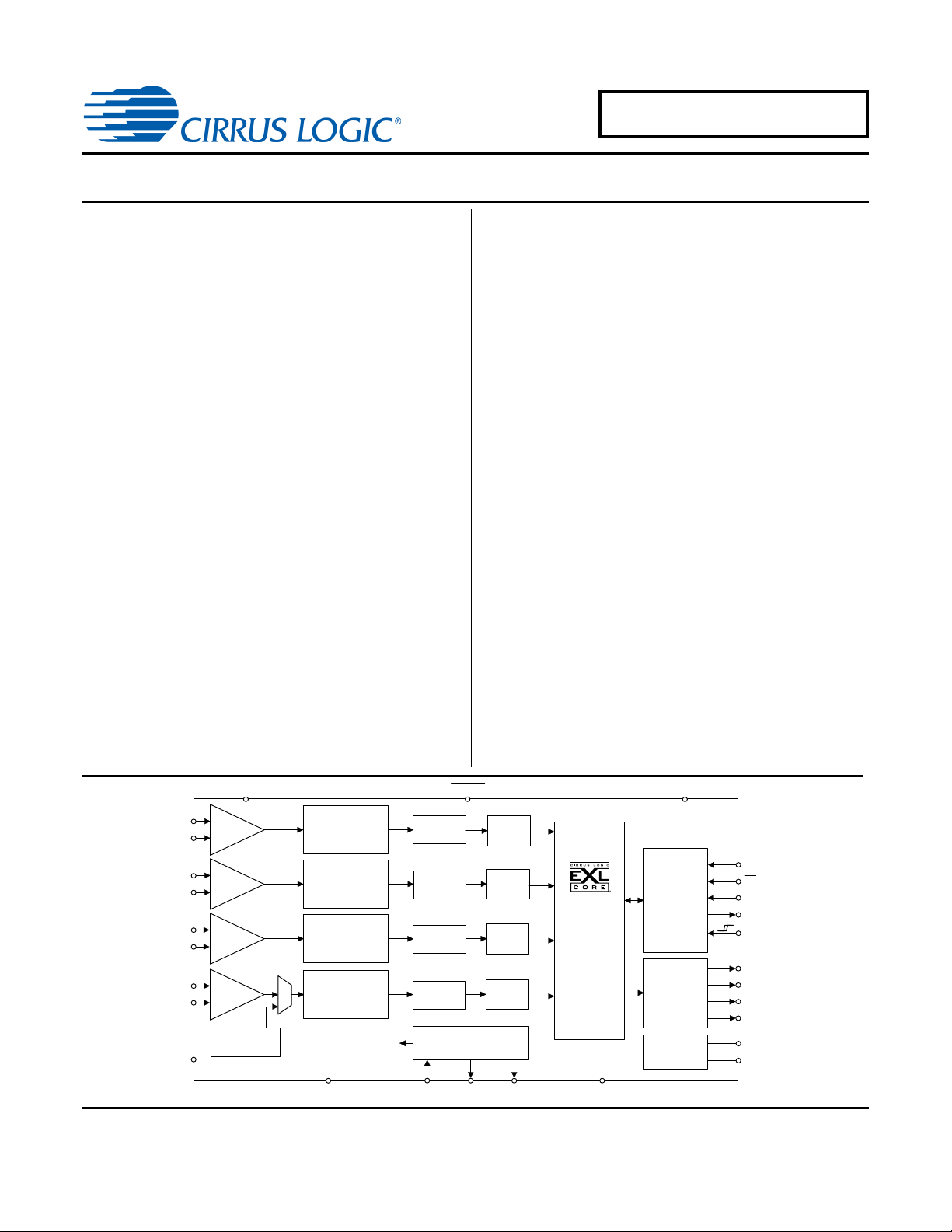
Four Channel Energy Measurement IC
Features & Description
• Superior Analog Performance with Ultra-low Noise Level
and High SNR
• Energy Measurement Accuracy of 0.1% over 4000:1
Dynamic Range
• Current RMS Measurement Accuracy of 0.1% over 1000:1
Dynamic Range
• 4 Independent 24-bit, 4
for Voltage and Current Measurements
• 4 Configurable Digital Outputs for Energy Pulses,
Zero-crossing, or Energy Direction
• Supports Shunt Resistor, CT, and Rogowski Coil Current
Sensors
• On-chip Measurements/Calculations:
- Active, Reactive, and Apparent Power
- RMS Voltage and Current
- Power Factor and Line Frequency
- Instantaneous Voltage, Current, and Power
• Overcurrent, Voltage Sag, and Voltage Swell Detection
• Ultra-fast On-chip Digital Calibration
• Internal Register Protection via Checksum and Write
Protection
• UART/SPI™ Serial Interface
• On-chip Temperature Sensor
• On-chip Voltage Reference (25ppm/°C Typ.)
• Single 3.3V Power Supply
• Ultra-fine Phase Compensation
• Low Power Consumption: <13mW
• Power Supply Configurations
- GNDA = GNDD = 0V, VDDA = +3.3V
• 5mmx5mm 28-pin QFN Package
ORDERING INFORMATION
See Page 68.
th
-order, Delta-Sigma Modulators
Description
The CS5484 is a high-accuracy, four-channel, energy
measurement analog front end.
The CS5484 incorporates independent 4th order Delta-Sigma
analog-to-digital converters for every channel, reference
circuitry, and the proven EXL signal processing core to provide
active, reactive, and apparent energy measurement. In
addition, RMS and power factor calculations are available.
Calculations are output through a configurable energy pulse,
or direct UART/SPI™ serial access to on-chip registers.
Instantaneous current, voltage, and power measurements are
also available over the serial port. Multiple serial options are
offered to allow customer flexibility. The SPI provides higher
speed, and the 2-wire UART minimizes the cost of isolation
where required.
Four configurable digital outputs provide energy pulses,
zero-crossing, energy direction, and interrupt functions.
Interrupts can be generated for a variety of conditions
including voltage sag or swell, overcurrent, and more. On-chip
register integrity is assured via checksum and write protection.
The CS5484 is designed to interface to a variety of voltage and
current sensors including shunt resistors, current
transformers, and Rogowski coils.
On-chip functionality makes digital calibration simple and
ultra-fast, minimizing the time required at the end of the
customer production line. Performance across temperature is
ensured with an on-chip voltage reference with low drift. A
single 3.3V power supply is required, and power consumption
is low at <13mW. To minimize space requirements, the
CS5484 is offered in a low-cost, 5mm x5mm 28-pin QFN
package.
Cirrus Logic, Inc.
http://www.cirrus.com
Copyright Cirrus Logic, Inc. 2013
(All Rights Reserved)
MAR’13
DS981F3
Page 2

CS5484
TABLE OF CONTENTS
1. Overview . . . . . . . . . . . . . . . . . . . . . . . . . . . . . . . . . . . . . . . . . . . . . . . . . . . . . . . . . . . . . . . .5
2. Pin Descriptions . . . . . . . . . . . . . . . . . . . . . . . . . . . . . . . . . . . . . . . . . . . . . . . . . . . . . . . . . .6
2.1 Analog Pins . . . . . . . . . . . . . . . . . . . . . . . . . . . . . . . . . . . . . . . . . . . . . . . . . . . . . . . .7
2.1.1 Voltage Inputs . . . . . . . . . . . . . . . . . . . . . . . . . . . . . . . . . . . . . . . . . . . . . . . . .7
2.1.2 Current Inputs . . . . . . . . . . . . . . . . . . . . . . . . . . . . . . . . . . . . . . . . . . . . . . . . .7
2.1.3 Voltage Reference . . . . . . . . . . . . . . . . . . . . . . . . . . . . . . . . . . . . . . . . . . . . .7
2.1.4 Crystal Oscillator . . . . . . . . . . . . . . . . . . . . . . . . . . . . . . . . . . . . . . . . . . . . . . . 7
2.2 Digital Pins . . . . . . . . . . . . . . . . . . . . . . . . . . . . . . . . . . . . . . . . . . . . . . . . . . . . . . . . .7
2.2.1 Reset Input . . . . . . . . . . . . . . . . . . . . . . . . . . . . . . . . . . . . . . . . . . . . . . . . . . .7
2.2.2 CPU Clock Output . . . . . . . . . . . . . . . . . . . . . . . . . . . . . . . . . . . . . . . . . . . . . . 7
2.2.3 Digital Outputs . . . . . . . . . . . . . . . . . . . . . . . . . . . . . . . . . . . . . . . . . . . . . . . .7
2.2.4 UART/SPI™ Serial Interface . . . . . . . . . . . . . . . . . . . . . . . . . . . . . . . . . . . . . . 8
2.2.5 SPI . . . . . . . . . . . . . . . . . . . . . . . . . . . . . . . . . . . . . . . . . . . . . . . . . . . . . . . . .8
2.2.6 UART . . . . . . . . . . . . . . . . . . . . . . . . . . . . . . . . . . . . . . . . . . . . . . . . . . . . . . .8
2.2.7 MODE Pin . . . . . . . . . . . . . . . . . . . . . . . . . . . . . . . . . . . . . . . . . . . . . . . . . . . .8
3. Characteristics and Specifications . . . . . . . . . . . . . . . . . . . . . . . . . . . . . . . . . . . . . . . . . . .9
4. Signal Flow Description . . . . . . . . . . . . . . . . . . . . . . . . . . . . . . . . . . . . . . . . . . . . . . . . . . .17
4.1 Analog-to-Digital Converters . . . . . . . . . . . . . . . . . . . . . . . . . . . . . . . . . . . . . . . . . .17
4.2 Decimation Filters . . . . . . . . . . . . . . . . . . . . . . . . . . . . . . . . . . . . . . . . . . . . . . . . . .17
4.3 IIR Filters . . . . . . . . . . . . . . . . . . . . . . . . . . . . . . . . . . . . . . . . . . . . . . . . . . . . . . . . .17
4.4 Phase Compensation . . . . . . . . . . . . . . . . . . . . . . . . . . . . . . . . . . . . . . . . . . . . . . .17
4.5 DC Offset and Gain Correction . . . . . . . . . . . . . . . . . . . . . . . . . . . . . . . . . . . . . . . .18
4.6 High-pass and Phase Matching Filters . . . . . . . . . . . . . . . . . . . . . . . . . . . . . . . . . .18
4.7 Digital Integrators . . . . . . . . . . . . . . . . . . . . . . . . . . . . . . . . . . . . . . . . . . . . . . . . . . .18
4.8 Low-rate Calculations . . . . . . . . . . . . . . . . . . . . . . . . . . . . . . . . . . . . . . . . . . . . . . . 18
4.8.1 Fixed Number of Samples Averaging . . . . . . . . . . . . . . . . . . . . . . . . . . . . . .18
4.8.2 Line-cycle Synchronized Averaging . . . . . . . . . . . . . . . . . . . . . . . . . . . . . . .19
4.8.3 RMS Current and Voltage . . . . . . . . . . . . . . . . . . . . . . . . . . . . . . . . . . . . . . . 19
4.8.4 Active Power . . . . . . . . . . . . . . . . . . . . . . . . . . . . . . . . . . . . . . . . . . . . . . . . .19
4.8.5 Reactive Power . . . . . . . . . . . . . . . . . . . . . . . . . . . . . . . . . . . . . . . . . . . . . . .19
4.8.6 Apparent Power . . . . . . . . . . . . . . . . . . . . . . . . . . . . . . . . . . . . . . . . . . . . . .19
4.8.7 Peak Voltage and Current . . . . . . . . . . . . . . . . . . . . . . . . . . . . . . . . . . . . . . .19
4.8.8 Power Factor . . . . . . . . . . . . . . . . . . . . . . . . . . . . . . . . . . . . . . . . . . . . . . . . . 19
4.9 Average Active Power Offset . . . . . . . . . . . . . . . . . . . . . . . . . . . . . . . . . . . . . . . . . .20
4.10 Average Reactive Power Offset . . . . . . . . . . . . . . . . . . . . . . . . . . . . . . . . . . . . . . .20
5. Functional Description . . . . . . . . . . . . . . . . . . . . . . . . . . . . . . . . . . . . . . . . . . . . . . . . . . . .21
5.1 Power-on Reset . . . . . . . . . . . . . . . . . . . . . . . . . . . . . . . . . . . . . . . . . . . . . . . . . . . .21
5.2 Power Saving Modes . . . . . . . . . . . . . . . . . . . . . . . . . . . . . . . . . . . . . . . . . . . . . . . .21
5.3 Zero-crossing Detection . . . . . . . . . . . . . . . . . . . . . . . . . . . . . . . . . . . . . . . . . . . . . .21
5.4 Line Frequency Measurement . . . . . . . . . . . . . . . . . . . . . . . . . . . . . . . . . . . . . . . . .22
5.5 Energy Pulse Generation . . . . . . . . . . . . . . . . . . . . . . . . . . . . . . . . . . . . . . . . . . . . .22
5.5.1 Pulse Rate . . . . . . . . . . . . . . . . . . . . . . . . . . . . . . . . . . . . . . . . . . . . . . . . . .24
5.5.2 Pulse Width . . . . . . . . . . . . . . . . . . . . . . . . . . . . . . . . . . . . . . . . . . . . . . . . . . 24
5.6 Voltage Sag, Voltage Swell, and Overcurrent Detection . . . . . . . . . . . . . . . . . . . . .24
2 DS981F3
Page 3

CS5484
5.7 Phase Sequence Detection . . . . . . . . . . . . . . . . . . . . . . . . . . . . . . . . . . . . . . . . . . . 25
5.8 Temperature Measurement . . . . . . . . . . . . . . . . . . . . . . . . . . . . . . . . . . . . . . . . . . . 25
5.9 Anti-creep . . . . . . . . . . . . . . . . . . . . . . . . . . . . . . . . . . . . . . . . . . . . . . . . . . . . . . . . 26
5.10 Register Protection . . . . . . . . . . . . . . . . . . . . . . . . . . . . . . . . . . . . . . . . . . . . . . . . 26
5.10.1 Write Protection . . . . . . . . . . . . . . . . . . . . . . . . . . . . . . . . . . . . . . . . . . . . . 26
5.10.2 Register Checksum . . . . . . . . . . . . . . . . . . . . . . . . . . . . . . . . . . . . . . . . . . 26
6. Host Commands and Registers . . . . . . . . . . . . . . . . . . . . . . . . . . . . . . . . . . . . . . . . . . . . 27
6.1 Host Commands . . . . . . . . . . . . . . . . . . . . . . . . . . . . . . . . . . . . . . . . . . . . . . . . . . . 27
6.1.1 Memory Access Commands . . . . . . . . . . . . . . . . . . . . . . . . . . . . . . . . . . . . . 27
6.1.1.1 Page Select . . . . . . . . . . . . . . . . . . . . . . . . . . . . . . . . . . . . . . . . . . . . 27
6.1.1.2 Register Read . . . . . . . . . . . . . . . . . . . . . . . . . . . . . . . . . . . . . . . . . . 27
6.1.1.3 Register Write . . . . . . . . . . . . . . . . . . . . . . . . . . . . . . . . . . . . . . . . . . 27
6.1.2 Instructions . . . . . . . . . . . . . . . . . . . . . . . . . . . . . . . . . . . . . . . . . . . . . . . . . . 27
6.1.3 Checksum . . . . . . . . . . . . . . . . . . . . . . . . . . . . . . . . . . . . . . . . . . . . . . . . . . . 28
6.1.4 Serial Time Out . . . . . . . . . . . . . . . . . . . . . . . . . . . . . . . . . . . . . . . . . . . . . . . 28
6.2 Hardware Registers Summary (Page 0) . . . . . . . . . . . . . . . . . . . . . . . . . . . . . . . . . 29
6.3 Software Registers Summary (Page 16) . . . . . . . . . . . . . . . . . . . . . . . . . . . . . . . . . 31
6.4 Software Registers Summary (Page 17) . . . . . . . . . . . . . . . . . . . . . . . . . . . . . . . . . 33
6.5 Software Registers Summary (Page 18) . . . . . . . . . . . . . . . . . . . . . . . . . . . . . . . . . 34
6.6 Register Descriptions . . . . . . . . . . . . . . . . . . . . . . . . . . . . . . . . . . . . . . . . . . . . . . .35
7. System Calibration . . . . . . . . . . . . . . . . . . . . . . . . . . . . . . . . . . . . . . . . . . . . . . . . . . . . . . . 62
7.1 Calibration in General . . . . . . . . . . . . . . . . . . . . . . . . . . . . . . . . . . . . . . . . . . . . . . . 62
7.1.1 Offset Calibration . . . . . . . . . . . . . . . . . . . . . . . . . . . . . . . . . . . . . . . . . . . . . 62
7.1.1.1 DC Offset Calibration . . . . . . . . . . . . . . . . . . . . . . . . . . . . . . . . . . . . 62
7.1.1.2 AC Offset Calibration . . . . . . . . . . . . . . . . . . . . . . . . . . . . . . . . . . . . . 63
7.1.2 Gain Calibration . . . . . . . . . . . . . . . . . . . . . . . . . . . . . . . . . . . . . . . . . . . . . . 63
7.1.3 Calibration Order . . . . . . . . . . . . . . . . . . . . . . . . . . . . . . . . . . . . . . . . . . . . . 63
7.2 Phase Compensation . . . . . . . . . . . . . . . . . . . . . . . . . . . . . . . . . . . . . . . . . . . . . . . 63
7.3 Temperature Sensor Calibration . . . . . . . . . . . . . . . . . . . . . . . . . . . . . . . . . . . . . . .65
7.3.1 Temperature Offset and Gain Calibration . . . . . . . . . . . . . . . . . . . . . . . . . . . 65
8. Basic Application Circuits . . . . . . . . . . . . . . . . . . . . . . . . . . . . . . . . . . . . . . . . . . . . . . . . . 66
9. Package Dimensions . . . . . . . . . . . . . . . . . . . . . . . . . . . . . . . . . . . . . . . . . . . . . . . . . . . . . 67
10. Ordering Information . . . . . . . . . . . . . . . . . . . . . . . . . . . . . . . . . . . . . . . . . . . . . . . . . . . .68
11. Environmental, Manufacturing, and Handling Information . . . . . . . . . . . . . . . . . . . . . 68
12. Revision History . . . . . . . . . . . . . . . . . . . . . . . . . . . . . . . . . . . . . . . . . . . . . . . . . . . . . . . . 68
DS981F3 3
Page 4

CS5484
LIST OF FIGURES
Figure 1. Oscillator Connections................................................................................................... 7
Figure 2. Multi-device UART Connections.................................................................................... 8
Figure 3. UART Serial Frame Format........................................................................................... 8
Figure 4. Active Energy Load Performance.................................................................................. 9
Figure 5. Reactive Energy Load Performance............................................................................ 10
Figure 6. IRMS Load Performance ............................................................................................. 10
Figure 7. SPI Data and Clock Timing ......................................................................................... 15
Figure 8. Multi-Device UART Timing .......................................................................................... 15
Figure 9. Signal Flow for V1, I1, P1, and Q1 Measurements ..................................................... 17
Figure 10. Signal Flow for V2, I2, P2, and Q2 Measurements ................................................... 17
Figure 11. Low-rate Calculations ................................................................................................18
Figure 12. Power-on Reset Timing ............................................................................................. 21
Figure 13. Zero-crossing Level and Zero-crossing Output on DOx ............................................ 22
Figure 14. Energy Pulse Generation and Digital Output Control ................................................ 23
Figure 15. Sag, Swell, and Overcurrent Detect .......................................................................... 24
Figure 16. Phase Sequence A, B, C for Rising Edge Transition ................................................ 25
Figure 17. Phase Sequence C, B, A for Rising Edge Transition ................................................ 26
Figure 18. Byte Sequence for Page Select................................................................................. 27
Figure 19. Byte Sequence for Register Read ............................................................................ 27
Figure 20. Byte Sequence for Register Write ............................................................................. 27
Figure 21. Byte Sequence for Instructions.................................................................................. 27
Figure 22. Byte Sequence for Checksum ................................................................................... 28
Figure 23. Calibration Data Flow ................................................................................................62
Figure 24. T Register vs. Force Temp ........................................................................................ 65
Figure 25. Typical Connection (Single-phase, 3-wire, 12S Electricity Meter)............................. 66
LIST OF TABLES
Table 1. POR Thresholds . . . . . . . . . . . . . . . . . . . . . . . . . . . . . . . . . . . . . . . . . . . . . . . . . . . . . 21
Table 2. Command Format . . . . . . . . . . . . . . . . . . . . . . . . . . . . . . . . . . . . . . . . . . . . . . . . . . . . 27
Table 3. Instruction Format . . . . . . . . . . . . . . . . . . . . . . . . . . . . . . . . . . . . . . . . . . . . . . . . . . . . 28
4 DS981F3
Page 5

CS5484
1. OVERVIEW
The CS5484 is a CMOS power measurement integrated circuit using four analog-to-digital converters
to measure two line voltages and two currents. Optionally, voltage2 channel can be used for temperature
measurement. It calculates active, reactive, and apparent power as well as RMS voltage and current and
peak voltage and current. It handles other system-related functions, such as energy pulse generation,
voltage sag and swell, overcurrent and zero-crossing detection, and line frequency measurement.
The CS5484 is optimized to interface to current transformers, shunt resistors, or Rogowski coils for
current measurement and to resistive dividers or voltage transformers for voltage measurement. Two
full-scale ranges are provided on the current inputs to accommodate different types of current sensors.
The CS5484’s four differential inputs have a common-mode input range from analog ground (GNDA) to
the positive analog supply (VDDA).
An on-chip voltage reference (typically 2.4 volts) is generated and provided at analog output, VREF±.
Four digital outputs (DO1, DO2, DO3, and DO4) provide a variety of output signals, and depending on the
mode selected, provide energy pulses, zero-crossings, or other choices.
The CS5484 includes a UART/SPI™ serial host interface to an external microcontroller. The serial select
(SSEL) pin is used to configure the serial port to be a SPI or UART. SPI signals include serial data input
(SDI), serial data output (SDO), and serial clock (SCLK). UART signals include serial data input (RX) and
serial data output (TX). A chip select (CS
interface with the microcontroller.
) signal allows multiple CS5484s to share the same serial
DS981F3 5
Page 6
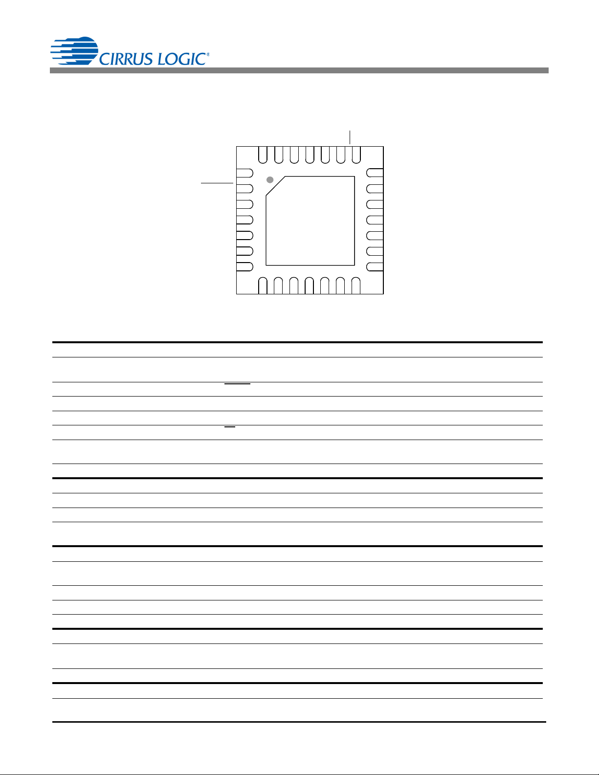
2. PIN DESCRIPTIONS
98
7
6
5
4
3
2
1
10
11
12 13 14
15
16
17
18
19
20
21
222324
25
262728
Top-Down View
28-pin QFN Pack age
Thermal Pad
XOUT
VDDD
GNDD
CPUCLK
MODE
SSEL
CS
VIN1-
IIN2-
IIN2+
VREF-
VREF+
GNDA
VDDA
XIN
RESET
IIN1-
IIN1+
VIN2-
VIN2+
VIN1+
SCLK
RX/SDI
TX/SDO
DO4
DO3
DO2
DO1
Do Not Connect
CS5484
Digital Pins and Serial Data I/O
Digital Outputs 15,16,
17,18
Reset 2
Serial Data I/O 19,20
Serial Clock Input 21
Chip Select 22
Serial Mode Select 23
Operating Mode Select 24
DO1, DO2, DO3, DO4 — Configurable digital outputs for energy pulses, interrupt, energy
direction, and zero-crossings.
RESET — An active-low Schmitt-trigger input used to reset the chip.
TX/ SDO, RX/SDI — UART /SPI serial data output/input.
SCLK — Serial clock for the SPI.
CS — Chip select for the UART/SPI.
SSEL — Selects the type of serial interface, UART or SPI™. Logic level one - UART
selected. Logic level zero - SPI selected.
MODE — Connect to VDDA for proper operation.
Analog Inputs/ Outputs
Voltage Inputs 7,8,6,5
Current Inputs 4,3,10,9
Voltage Reference Input 12,11
VIN1+, VIN1-, VIN2+, VIN2- — Differential analog inputs for the voltage channels.
IIN1+, IIN1-, IIN2+, IIN2- — Differential analog inputs for the current channels.
VREF+, VREF- — The internal voltage reference. A 0.1µF bypass capacitor is required
between these two pins.
Power Supply Connections
Internal Digital Supply 27
Digital Ground 26
Positive Analog Supply 14
Analog Ground 13
Clock Generator
Crystal In
Crystal Out
CPU Clock Output 25
Thermal Pad
6 DS981F3
1,28
VDDD — Decoupling pin for the internal 1.8 V digital supply. A 0.1µF bypass capacitor is
required between this pin and GNDD.
GNDD — Digital ground.
VDDA — The positive 3.3V analog supply.
GNDA — Analog ground.
XIN, XOUT — Connect to an external quartz crystal. Alternatively, an external clock can be
supplied to the XIN pin to provide the system clock for the device.
CPUCLK — Output of on-chip oscillator which can drive one standard CMOS load.
No Electrical Connection.
-
Page 7
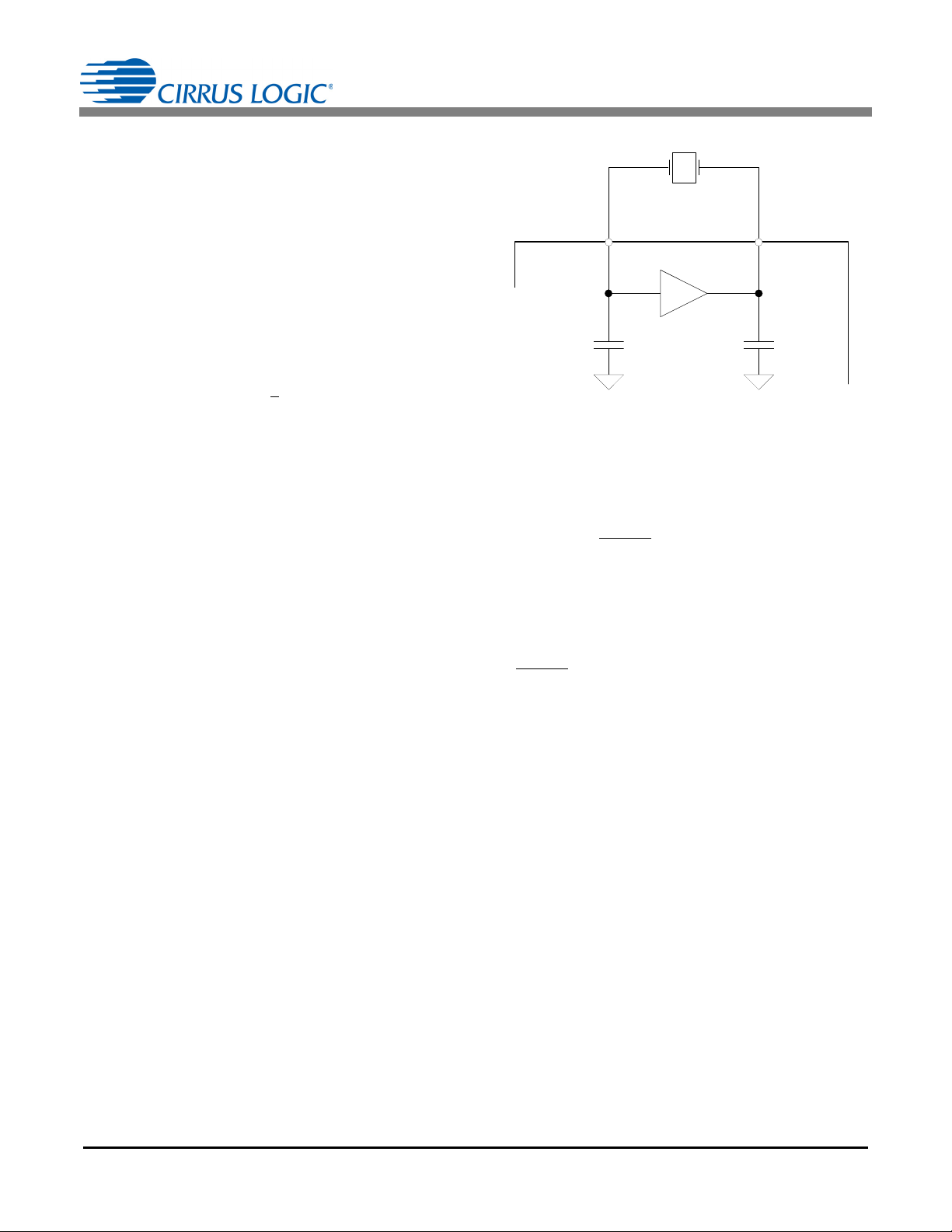
2.1 Analog Pins
XIN XOUT
C1 = 22pF C2 = 22pF
Figure 1. Oscillator Connections
The CS5484 has two differential inputs (VIN1VIN2)
for voltage input and two differential inputsIIN1 IIN2)
for current1 and current2 inputs. The CS5484 also has
two voltage reference pins (VREF) between which a
bypass capacitor should be placed.
2.1.1 Voltage Inputs
The output of the line voltage resistive divider or
transformer is connected to the VIN1 or VIN2 input
pins of the CS5484. The voltage channel is equipped
with a 10x, fixed-gain amplifier. The full-scale signal
level that can be applied to the voltage channel is
±250mV. If the input signal is a sine wave, the maximum
RMS voltage is 250mVp /
approximately 70.7% of maximum peak voltage.
2.1.2 Current Inputs
The output of the current-sensing shunt resistor,
transformer, or Rogowski coil is connected to the
IIN1 or IIN2 input pins of the CS5484. To
accommodate different current-sensing elements, the
current channel incorporates a programmable gain
amplifier (PGA) with two selectable input gains, as
described in the Config0 register description (see
section 6.6.1 Configuration 0 (Config0) – Page 0,
Address 0 on page 35.) There is a 10x gain setting and
a 50x gain setting. The full-scale signal level for current
channels is ±50mV and ±250 mV for 50x and 10x gain
settings, respectively. If the input signal is a sine wave,
the maximum RMS voltage is 35.35mV
176.78mV
maximum peak voltage.
which is approximately 70.7% of
RMS,
2.1.3 Voltage Reference
The CS5484 generates a stable voltage reference of
2.4V between the VREF pins. The reference system
also requires a filter capacitor of at least 0.1µF between
the VREF pins.
The reference system is capable of providing a
reference for the CS5484 but has limited ability to drive
external circuitry. It is strongly recommended that
nothing other than the required filter capacitor be
connected to the VREF pins.
2.1.4 Crystal Oscillator
An external, 4.096 MHz quartz crystal can be connected
to the XIN and XOUT pins, as shown in Figure 1. To reduce system cost, each pin is supplied with an on-chip
load capacitor.
2 176.78mV
RMS
, which is
or
RMS
CS5484
Alternatively, an external clock source can be
connected to the XIN pin.
2.2 Digital Pins
2.2.1 Reset Input
The active-low RESET pin, when asserted for longer
than 120µs, will halt all CS5484 operations and reset
internal hardware registers and states. When
de-asserted, an initialization sequence begins, setting
default register values. To prevent erroneous
noise-induced resets to the CS5484, an external pull-up
resistor and a decoupling capacitor are necessary on
the RESET
2.2.2 CPU Clock Output
A logic-level clock output (CPUCLK) is provided at the
crystal frequency to drive another CS5484 IC or
external microcontroller. Writing ‘1’ to bit CPUCLK_ON
of the Config0 register enables the CPU clock output.
After the CPU clock output is enabled, it can be disabled
only by a power-on reset (POR) or by writing ‘0’ to the
CPUCLK_ON bit. A hardware reset through pin/RESET
or a software reset instruction through the serial
interface will not disable the CPU clock output. Two
phase choices are available on the CPUCLK pin
through bit iCPUCLK of the Config0 register. Different
from the CPUCLK_ON bit, the iCPUCLK bit can be
cleared by a POR, a hardware reset, a software reset
instruction, or a register write.
2.2.3 Digital Outputs
The CS5484 provides four configurable digital outputs
(DO1-DO4). They can be configured to output energy
pulses, interrupt, zero-crossings, or energy directions.
Refer to section 6.6.2 Configuration 1 (Config1) – Page
0, Address 1 on page 36 for more details.
pin.
DS981F3 7
Page 8
CS5484
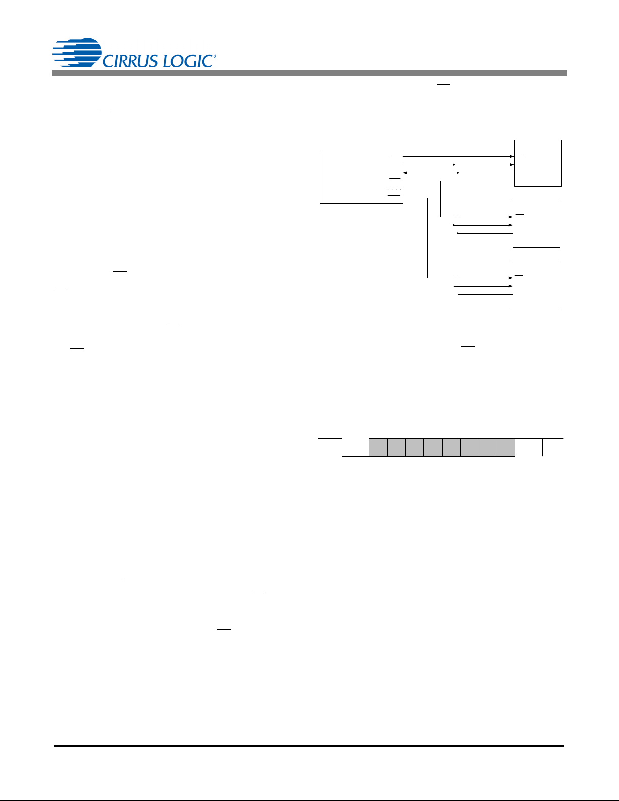
UART
MASTER
SLAVE 0
SLAVE 1
SLAVE N
CS
RX
TX
CS
RX
TX
CS
RX
TX
CS0
CS1
CSN
RX
TX
0 1 2 7IDLE STOP3 4 5 6START
DATA
IDLE
2.2.4 UART/SPI™ Serial Interface
The CS5484 provides five pins—SSEL, RX/SDI,
TX/SDO, CS
, and SCLK—for communication between
a host microcontroller and the CS5484.
SSEL is an input that, when low, indicates to the
CS5484 to use the SPI port as the serial interface to
communicate with the host microcontroller. The SSEL
pin has an internal weak pull-up. When the SSEL pin is
left unconnected or pulled high externally, the UART
port is used as the serial interface.
2.2.5 SPI
The CS5484 provides a Serial Peripheral Interface
(SPI) that operates as a slave device in 4-wire mode
and supports multiple slaves on the SPI bus. The 4-wire
SPI includes CS
CS
is the chip select input for the CS5484 SPI port. A
, SCLK, SDI, and SDO signals.
high logic level de-asserts it, tri-stating the SDO pin and
clearing the SPI interface. A low logic level enables the
SPI port. Although the CS
pin may be tied low for
systems that do not require multiple SDO drivers, using
the CS
signal is strongly recommended to achieve more
reliable SPI communications.
SCLK is the serial clock input for the CS5484 SPI port.
Serial data changes as a result of the falling edge of
SCLK and is valid at the rising edge. The SCLK pin is a
Schmitt-trigger input.
SDI is the serial data input to the CS5484.
SDO is the serial data output from the CS5484.
The CS5484 SPI transmits and receives data MSB first.
Refer to Switching Characteristics on page 14 and
Figure 7 on page 15 for more detailed information about
SPI timing.
2.2.6 UART
The CS5484 device contains an asynchronous,
full-duplex UART. The UART may be used in either
standard 2-wire communication mode (RX/TX) for
connecting a single device or 3-wire communication
mode (RX/TX/
When connecting a single CS5484 device, CS
be held low to enable the UART. Multiple CS5484
devices can communicate to the same master UART in
the 3-wire mode by pulling a slave CS
data transmissions. Common RX and TX signals are
provided to all the slave devices, and each slave device
CS) for connecting multiple devices.
should
pin low during
requires a separate CS
signal for enabling
communication to that slave. The multi-device UART
mode connections are shown in Figure 2.
Figure 2. Multi-device UART Connections
The multi-device UART mode timing diagram provides
the timing requirements for the CS
control (see Figure
8. Multi-Device UART Timing on Page 15).
The CS5484 UART operates in 8-bit mode, which
transmits a total of 10 bits per byte. Data is transmitted
and received LSB first, with one start bit, eight data bits,
and one stop bit.
Figure 3. UART Serial Frame Format
The baud rate is defined in the SerialCtrl register. After
chip reset, the default baud rate is 600, if MCLK is
4.096MHz. The baud rate is based on the contents of
bits BR[15:0] in the SerialCtrl register and is calculated
as follows:
BR[15:0] = Baud Rate x (524288/MCLK)
or
Baud Rate = BR[15:0] /(524288 / MCLK)
The maximum baud rate is 512K if MCLK is 4.096 MHz.
2.2.7 MODE Pin
The MODE pin must be tied to VDDA for normal
operation. The MODE pin is used primarily for factory
test procedures.
8 DS981F3
Page 9
CS5484
-1
-0.5
0
0.5
1
0 500 1000 1500 2000 2500 3000 3500 40 00 4500
Percent Error (%)
Current Dynamic Range (x : 1
)
Lagging PF = 0.5
Leading PF = 0.5
PF = 1
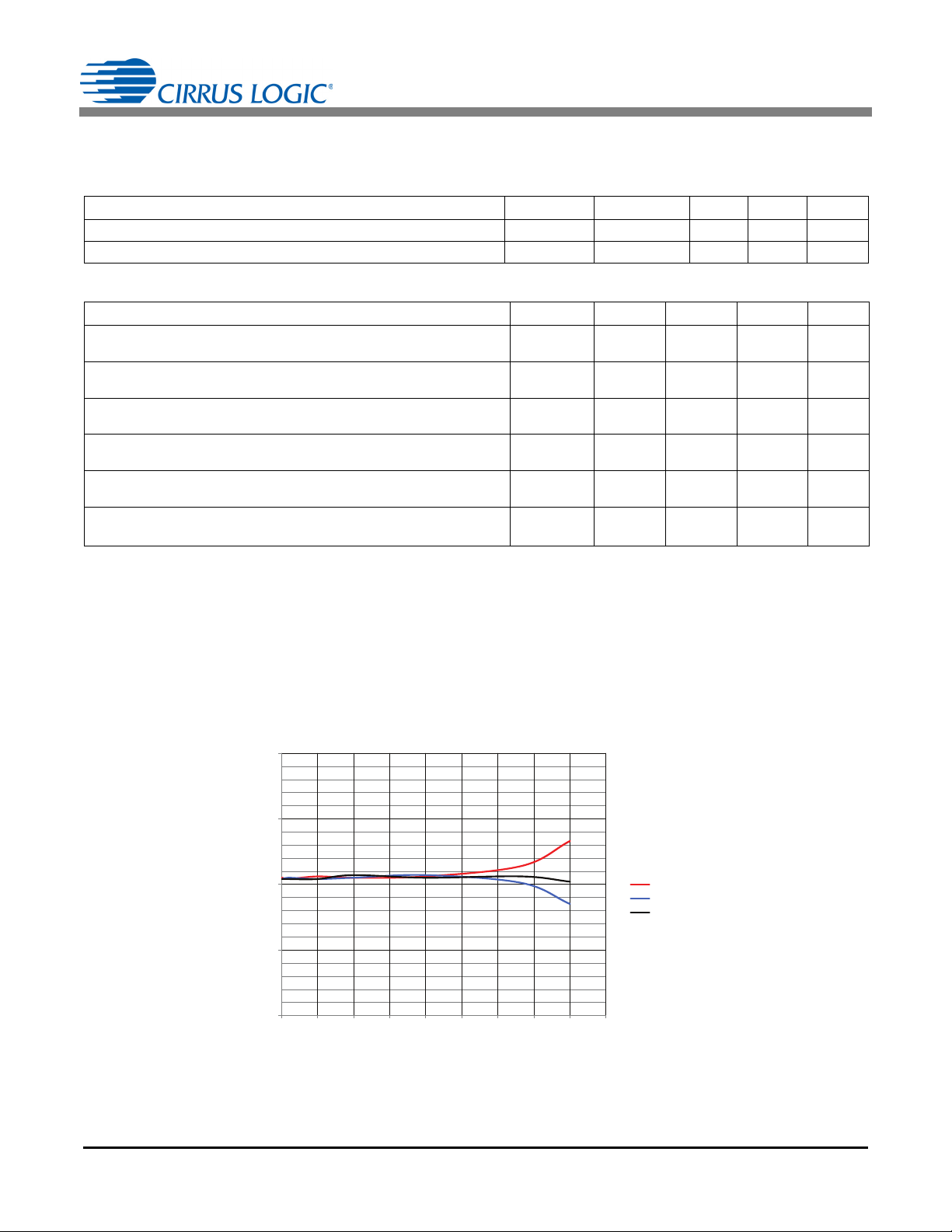
Figure 4. Active Energy Load Performance
3. CHARACTERISTICS AND SPECIFICATIONS
RECOMMENDED OPERATING CONDITIONS
Parameter Symbol Min Typ Max Unit
Positive Analog Power Supply VDDA 3.0 3.3 3.6 V
Specified Temperature Range T
POWER MEASUREMENT CHARACTERISTICS
Parameter Symbol Min Typ Max Unit
Active Energy
(Note 1 and 2) Current Channel Input Signal Dynamic Range 4000:1
Reactive Energy
(Note 1 and 2) Current Channel Input Signal Dynamic Range 4000:1
Apparent Power
(Note 1 and 3) Current Channel Input Signal Dynamic Range 1000:1
Current RMS
(Note 1, 3, and 4) Current Channel Input Signal Dynamic Range 1000:1
Voltage RMS
(Note 1 and 3) Voltage Channel Input Signal Dynamic Range 20:1
Power Factor All Gain Ranges
(Note 1 and 3) Current Channel Input Signal Dynamic Range 1000:1
Notes: 1. Specifications guaranteed by design and characterization.
2. Active energy is tested with power factor (PF) = 1.0. Reactive energy is tested with Sin(
system level using a single energy pulse. Where: 1) One energy pulse = 0.5Wh or 0.5 Varh; 2) VDDA = +3.3V, T
= 4.096MHz; 3) System is calibrated.
3. Calculated using register values; N
4. I
error calculated using register values. 1) VDDA = +3.3V; TA = 25°C; MCLK = 4.096MHz; 2) AC offset calibration applied.
RMS
≥4000.
All Gain Ranges
All Gain Ranges
All Gain Ranges
All Gain Ranges
A
P
Avg
Q
Avg
S-±0.1-%
I
RMS
V
RMS
PF - ±0.1 - %
-40 - +85 °C
-±0.1- %
-±0.1- %
-±0.1- %
-±0.1- %
) = 1.0. Energy error measured at
= 25°C, MCLK
A
TYPICAL LOAD PERFORMANCE
• Energy error measured at system level using single energy pulse; where one energy pulse = 0.5Wh or 0.5Varh
•I
error calculated using register values
RMS
• VDDA = +3.3V; T
= 25°C; MCLK = 4.096MHz
A
DS981F3 9
Page 10
CS5484
-1
-0.5
0
0.5
1
0 500 1000 1500 2000 2500 3000 3500 4000 4500
Percent Error (%)
Current Dynamic Range (x : 1
)
Lagging sin() = 0.5
Leading sin() = 0.5
sin() = 1
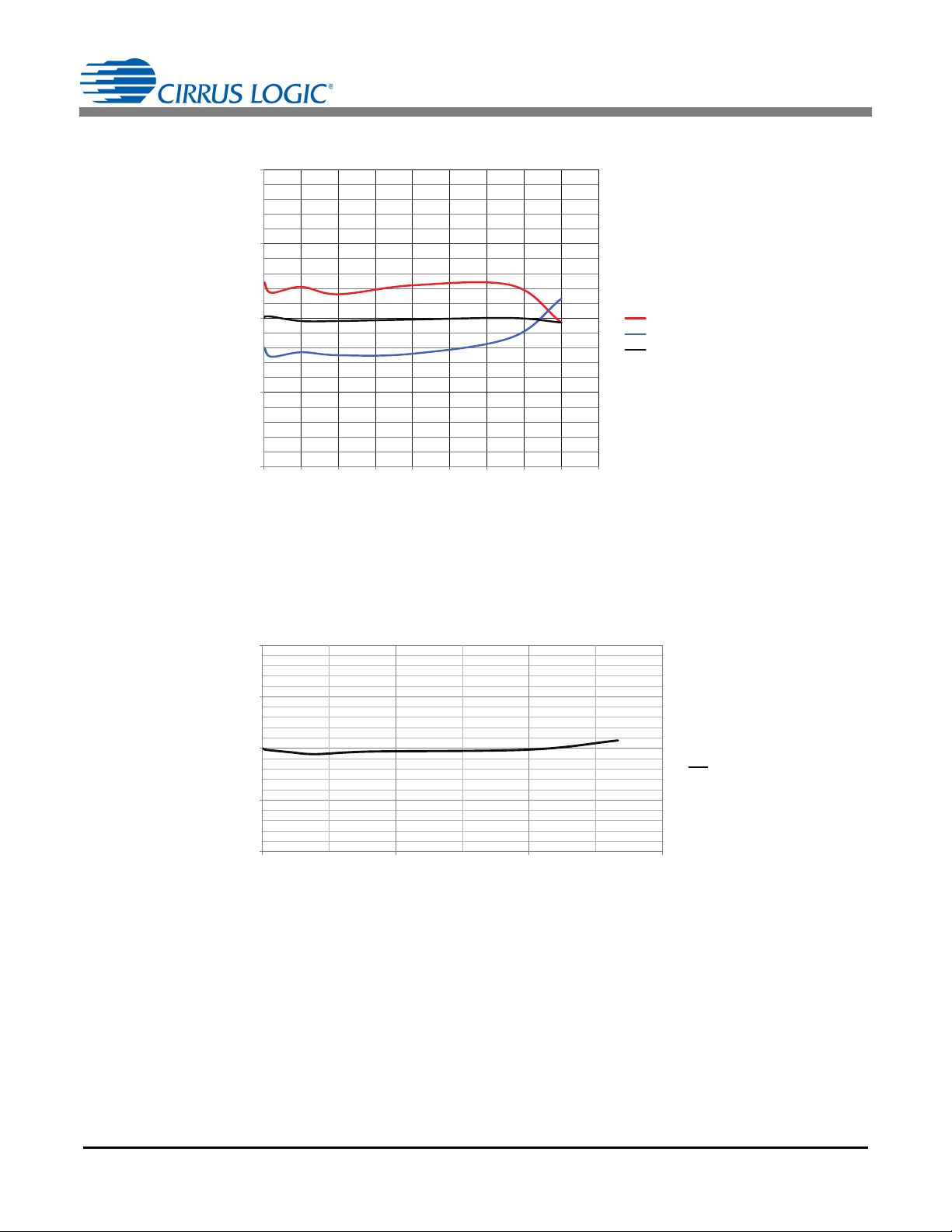
Figure 5. Reactive Energy Load Performance
-1
-0.5
0
0.5
1
0 500 1000 15 00
Percent Error (%)
Current Dynamic range (x : 1)
IRMS Error
I
Error
Figure 6. I
RMS
Load Performance
10 DS981F3
RMS
Page 11
ANALOG CHARACTERISTICS
CS5484
• Min / Max characteristics and specifications are guaranteed over all Recommended Operating Conditions.
• Typical characteristics and specifications are measured at nominal supply voltages and T
• VDDA = +3.3V ±10%; GNDA = GNDD = 0V. All voltages with respect to 0V.
• MCLK = 4.096MHz.
= 25°C.
A
Parameter Symbol Min Typ Max Unit
Analog Inputs (Current Channels)
Common Mode Rejection
(DC, 50, 60Hz) CMRR 80 - - dB
Common Mode+Signal -0.25 - VDDA V
Differential Full-scale Input Range
[(IIN+) – (IIN-)] (Gain = 50)
(Gain = 10)
IIN
-
-
250
50
-
-
mV
mV
P
P
Total Harmonic Distortion (Gain = 50) THD 90 100 - dB
Signal-to-Noise Ratio (SNR)
Crosstalk from Voltage Inputs at Full Scale
Crosstalk from Current Input at Full Scale
(Gain = 10)
(Gain = 50)
(50, 60Hz) --115-dB
(50, 60Hz) --115-dB
SNR
-
-
80
80
-
-
dB
dB
Input Capacitance IC - 27 - pF
Effective Input Impedance EII 30 - - k
Offset Drift (Without the High-pass Filter) OD - 4.0 - µV/°C
Noise (Referred to Input)
(Gain = 10)
(Gain = 50)
N
I
-
-
15
3.5
-
µV
µV
RMS
RMS
-
Power Supply Rejection Ratio (60Hz)
(Note 7) (Gain = 10)
(Gain = 50)
PSRR 60
68
65
75
-
-
dB
dB
Analog Inputs (Voltage Channels)
Common Mode Rejection
(DC, 50, 60Hz) CMRR 80 - - dB
Common Mode+Signal -0.25 - VDDA V
Differential Full-scale Input Range
[(VIN+) – (VIN-)] VIN - 250 - mV
P
Total Harmonic Distortion THD 80 88 - dB
Signal-to-Noise Ratio (SNR) SNR - 73 - dB
Crosstalk from Current Inputs at Full Scale
(50, 60Hz) --115-dB
Input Capacitance IC - 2.0 - pF
Effective Input Impedance EII 2 - - M
Noise (Referred to Input) N
V
-40-µV
RMS
Offset Drift (Without the High-pass Filter) OD - 16.0 - µV/°C
Power Supply Rejection Ratio
(Note 7) (Gain = 10)
(60Hz)
PSRR 60 65 - dB
Temperature
Temperature Accuracy
(Note 6) T-±5-°C
DS981F3 11
Page 12
Parameter Symbol Min Typ Max Unit
PSRR 20
150
V
eq
---------- -
log=
TC
VREF
VREF
MAX
VREF
MIN
–
VREF
AVG
------------------------------------------------------------
1
T
A
MAX TAMIN–
----------------------------------------------
1.0 10
6
=
Power Supplies
Power Supply Currents (Active State)
Power Consumption
(Note 5) Active State (VDDA = +3.3V)
Notes: 5. All outputs unloaded. All inputs CMOS level.
6. Temperature accuracy measured after calibration is performed.
7. Measurement method for PSRR: VDDA = +3.3V, a 150 mV (zero-to-peak) (60 Hz) sine wave is imposed onto the +3.3V DC
supply voltage at the VDDA pin. The “+” and “-” input pins of both input channels are shorted to GNDA. The CS5484 is then
commanded to continuous conversion acquisition mode, and digital output data is collected for the channel under test. The
(zero-to-peak) value of the digital sinusoidal output signal is determined, and this value is converted into the (zero-to-peak) value
of the sinusoidal voltage (measured in mV) that would need to be applied at the channel’s inputs in order to cause the same digital
sinusoidal output. This voltage is then defined as V
I
(VDDA = +3.3V) PSCA - 3.9 - mA
A+
Stand-by State
PSRR is (in dB):
eq
VOLTAGE REFERENCE
Parameter Symbol Min Typ Max Unit
PC -
CS5484
12.9
-
4.5
-
-
mW
mW
Reference
(Note 8)
Output Voltage VREF +2.3 +2.4 +2.5 V
Temperature Coefficient
Load Regulation
Notes: 8. It is strongly recommended that no connection other than the required filter capacitor be made to VREF±.
9. The voltage at VREF± is measured across the temperature range. From these measurements the following formula is used to
calculate the VREF temperature coefficient:
10. Specified at maximum recommended output of 1µA sourcing. VREF is a sensitive signal; the output of the VREF circuit has a
high output impedance so that the 0.1µF reference capacitor provides attenuation even to low-frequency noise, such as 50 Hz
noise on the VREF output. Therefore VREF intended for the CS5484 only and should not be connected to any external circuitry.
The output impedance is sufficiently high that standard digital multi-meters can significantly load this voltage. The accuracy of the
metrology IC cannot be guaranteed when a multimeter or any component other than the 0.1µF capacitor is attached to VREF. If
it is desired to measure VREF for any reason other than a very course indicator of VREF functionality, Cirrus recommends a very
high input impedance multimeter such as the Keithley Model 2000 Digital Multimeter be used. Cirrus cannot guarantee the
accuracy of the metrology with this meter connected to VREF.
(Note 9) TC
(Note 10) V
VREF
R
-25-ppm/°C
-30-mV
12 DS981F3
Page 13
CS5484
DIGITAL CHARACTERISTICS
• Min / Max characteristics and specifications are guaranteed over all Recommended Operating Conditions.
• Typical characteristics and specifications are measured at nominal supply voltages and T
• VDDA = +3.3V ±10%; GNDA = GNDD = 0V. All voltages with respect to 0 V.
• MCLK = 4.096MHz.
Parameter Symbol Min Typ Max Unit
Master Clock Characteristics
XIN Clock Frequency
Internal Gate Oscillator MCLK 2.5 4.096 5 MHz
Filter Characteristics
Phase Compensation Range
(60Hz, OWR = 4000Hz) -10.79 - +10.79 °
Input Sampling Rate - MCLK/8 - Hz
Digital Filter Output Word Rate
High-pass Filter Corner Frequency
(Both channels) OWR - MCLK/1024 - Hz
-3dB -2.0-Hz
Input/Output Characteristics
High-level Input Voltage (All Pins) V
Low-level Input Voltage (All Pins) V
High-level Output Voltage
(Note 12) All Other Outputs, I
Low-level Output Voltage
(Note 12) All Other Outputs, I
DO1-DO4, I
DO1-DO4, I
=+10mA
out
=+5mA
out
=-12mA
out
out
=-5mA
V
V
Input Leakage Current I
3-state Leakage Current I
Digital Output Pin Capacitance C
OZ
0.6(VDDA) - - V
IH
IL
OH
OL
in
--0.6V
VDDA-0.3
VDDA-0.3
-
-
-±1±10µA
--±10µA
out
-5-pF
= 25°C.
A
-
-
-
-
-
-
0.5
0.5
V
V
V
V
Notes: 11. All measurements performed under static conditions.
12. XOUT pin used for crystal only. Typical drive current< 1mA.
DS981F3 13
Page 14
CS5484
SWITCHING CHARACTERISTICS
• Min / Max characteristics and specifications are guaranteed over all Recommended Operating Conditions.
• Typical characteristics and specifications are measured at nominal supply voltages and T
• VDDA = +3.3V ±10%; GNDA = GNDD = 0V. All voltages with respect to 0V.
• Logic Levels: Logic 0 = 0 V, Logic 1 = VDDA.
Parameter Symbol Min Typ Max Unit
Rise Times
(Note 13) Any Digital Output Except DO1-DO4
Fall Times
(Note 13) Any Digital Output Except DO1-DO4
DO1-DO4
DO1-DO4
t
rise
t
fall
Start-up
Oscillator Start-up Time
XTAL = 4.096MHz (Note 14) t
ost
SPI Timing
Serial Clock Frequency (Note 15) SCLK - - 2 MHz
Serial Clock
Enable to SCLK Falling t
CS
Data Set-up Time prior to SCLK Rising t
Data Hold Time After SCLK Rising t
SCLK Rising Prior to CS
Disable t
SCLK Falling to New Data Bit t
Rising to SDO Hi-Z t
CS
Pulse Width High
Pulse Width Low
t
1
t
2
3
4
5
6
7
8
200
200
50 - - ns
50 - - ns
100 - - ns
UART Timing
Enable to RX START bit t
CS
STOP bit to CS
Disable to TX IDLE Hold Time t
CS
Notes: 13. Specified using 10% and 90% points on waveform of interest. Output loaded with 50pF.
14. Oscillator start-up time varies with crystal parameters. This specification does not apply when using an external clock source.
15. The maximum SCLK is 2MHz during a byte transaction. The minimum 1 µs idle time is required on the SCLK between two
Disable
consecutive bytes.
9
t
10
11
= 25°C.
A
-
-
-
-
50
50
-
-
1.0
-
1.0
-
µs
ns
µs
ns
-60-ms
-
-
-
-
ns
ns
1--µs
--150ns
--250ns
5--ns
1--µs
--250ns
14 DS981F3
Page 15
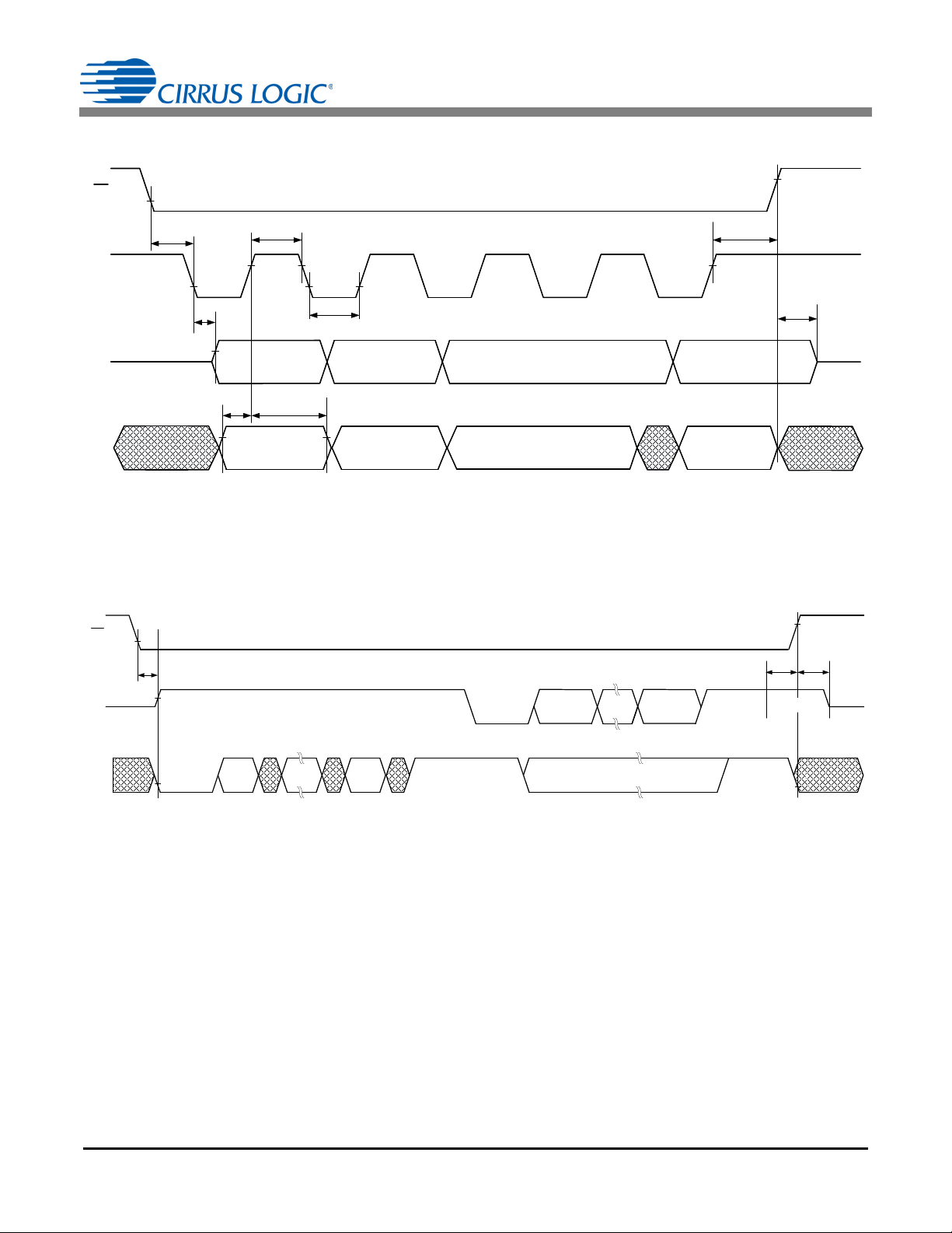
CS5484
SDO
SDI
t
1
t
2
t
3
t
4
t
5
t
6
t
7
t
8
CS
SCLK
MSB
MSB
MSB-1
MSB-1
INTERMED IAT E B ITS
INTERMED IAT E B ITS
LSB
LSB
Figure 7. SPI Data and Clock Timing
TX
RX
t
9
t
11
CS
START LSB
LSB
DATA MSB STOP
START DATA MS B
STOP
STOP
IDLE
OPTIONAL OVERLAP INSTRUCTION *
IDL E
t
10
IDLE
* Reading registers during the optional overlap instruction requires
the start to occur during the last byte transmitted by the part
Figure 8. Multi-Device UART Timing
DS981F3 15
Page 16
CS5484
ABSOLUTE MAXIMUM RATINGS
Parameter Symbol Min Typ Max Unit
DC Power Supplies
Input Current
Input Current for Power Supplies - - - ±50 -
Output Current
Power Dissipation
Input Voltage
Junction-to-Ambient Thermal Impedance
Ambient Operating Temperature T
Storage Temperature T
Notes: 16. VDDA and GNDA must satisfy [(VDDA) – (GNDA)] + 4.0V.
17. Applies to all pins, including continuous overvoltage conditions at the analog input pins.
18. Transient current of up to 100mA will not cause SCR latch-up.
19. Applies to all pins, except VREF±
20. Total power dissipation, including all input currents and output currents.
21. Applies to all pins.
.
(Note 16) VDDA -0.3 - +4.0 V
(Notes 17 and 18)
(Note 19)
(Note 20) PD -- 500mW
(Note 21) V
2 Layer Board
4 Layer Board
I
I
OUT
IN
IN
JA
A
stg
-- ±10mA
-- 100mA
- 0.3 - (VDDA) + 0.3 V
-
-
53
43
-
-
-40 - 85 °C
-65 - 150 °C
°C/W
°C/W
WARNING:
Operation at or beyond these limits may result in permanent damage to the device.
Normal operation is not guaranteed at these extremes.
16 DS981F3
Page 17
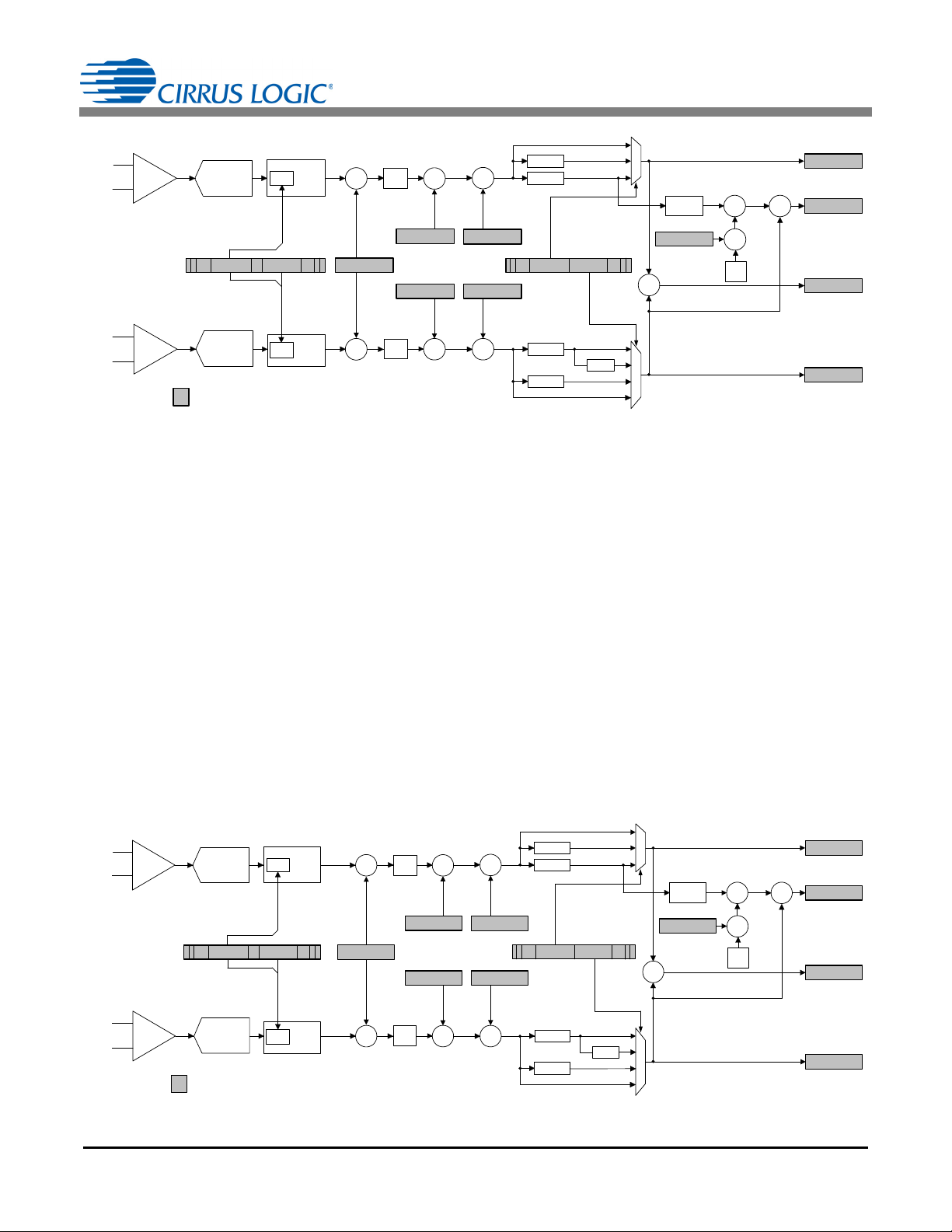
4. SIGNAL FLOW DESCRIPTION
MUX
VIN1±
SINC
3
+
X
IIN1±
SINC
3
+
X
PGA
+
+
HPF
4th Order
ΔΣ
Modulator
4th Order
ΔΣ
Modulator
x10
X
DELAY
CTRL
X
X
X
2
MUX
X
PMF
HPF
PMF
IIR
IIR
Phase
Shift
Config 2
X
Eps ilon
DELAY
CTRL
INT
Registers
Q1
V1
P1
I1
SYS
GAIN
... ...
I1FLT[1:0]V1FLT[ 1:0]
V1
DCOFF
I1
DCOFF
I1
GAIN
V1
GAIN
PC
... ...
FPCC1[8:0]CPCC1[1:0]
...
Figure 9. Signal Flow for V1, I1, P1, and Q1 Measurements
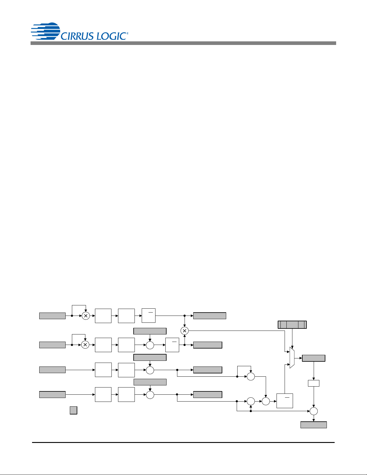
MUX
VIN2±
SINC
3
+
X
IIN2±
SINC
3
+
X
PGA
+
+
HPF
4th Order
ΔΣ
Modulator
4th Order
ΔΣ
Modulator
x10
X
DELAY
CTRL
X
X
X
2
MUX
X
PMF
HPF
PMF
IIR
IIR
Phase
Shift
X
Epsilon
DELAY
CTRL
INT
Regi ster s
Q2
V2
P2
I2
SYS
GAIN
V2
DCOFF
I2
DCOFF
I2
GAIN
V2
GAIN
PC
Config 2
... ...
I2FLT[1:0]
V2FLT[ 1:0]
... ...
FPCC2[8:0]CPCC2[1:0]
...
Figure 10. Signal Flow for V2, I2, P2, and Q2 Measurements
The signal flow for voltage measurement, current
measurement, and the other calculations is shown in
Figures 9, 10, and 11.
The signal flow consists of two current channels and two
voltage channels. The current and voltage channels
have differential input pins.
4.1 Analog-to-Digital Converters
All four input channels use fourth-order delta-sigma
modulators to convert the analog inputs to single-bit
digital data streams. The converters sample at a rate of
MCLK/8. This high sampling provides a wide dynamic
range and simplifies anti-alias filter design.
4.2 Decimation Filters
The single-bit modulator output data is widened to 24
bits and down sampled to MCLK/1024 with low-pass
decimation filters. These decimation filters are
CS5484
third-order Sinc filters. The filter outputs pass through
an IIR "anti-sinc" filter.
4.3 IIR Filters
The IIR filters are used to compensate for the amplitude
roll-off of the decimation filters. The droop-correction
filter flattens the magnitude response of the channel out
to the Nyquist frequency, thus allowing for accurate
measurements of up to 2 kHz (MCLK = 4.096 MHz). By
default, the IIR filters are enabled. The IIR filters can be
bypassed by setting the IIR_OFF bit in the Config2
register.
4.4 Phase Compensation
Phase compensation changes the phase of voltage
relative to current by adding a delay in the decimation
filters.
The amount of phase shift is set by the PC register
bits CPCCx[1:0] and FPCCx[8:0] for current channels.
Bits CPCCx[1:0] set the delay for the voltage channels.
DS981F3 17
Page 18
CS5484
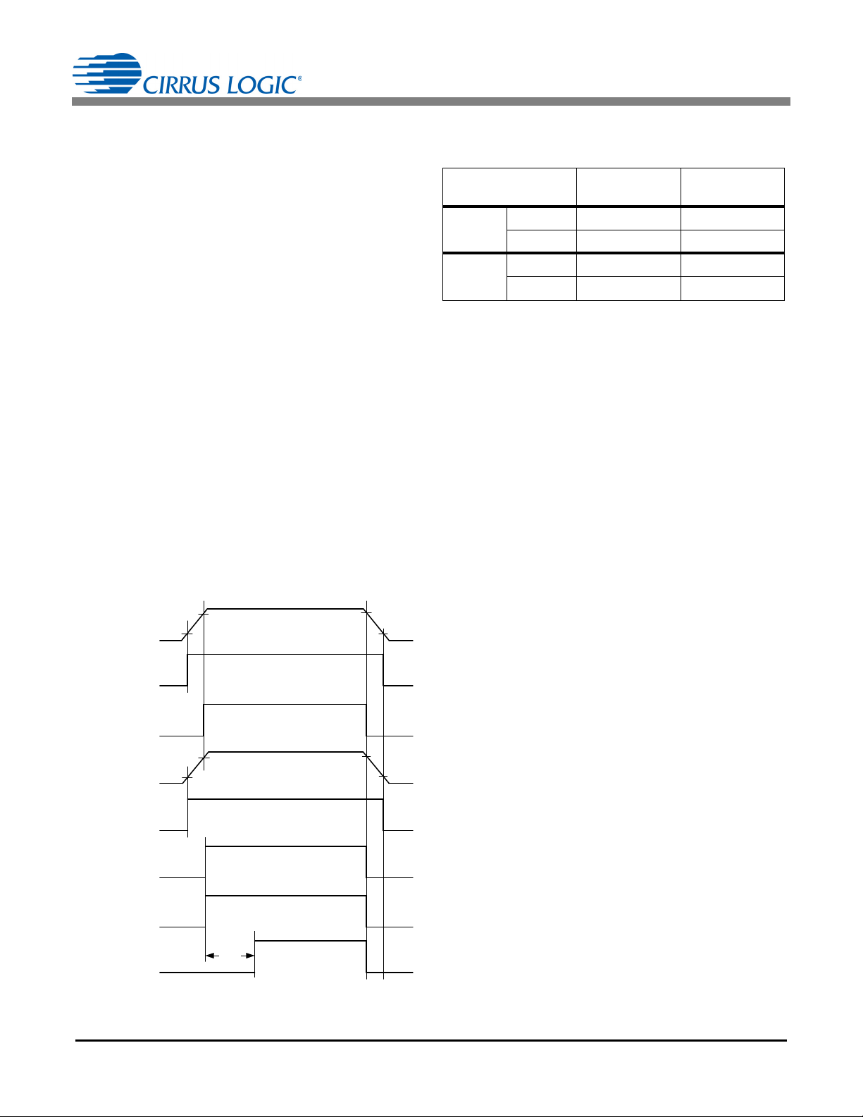
N
÷
N
N
÷
N
N
÷
N
N
÷
N
Regi ster s
MUX
...
...
APCM
Config 2
V1(V2)
I1 (I2)
P1 (P2)
Q1 (Q 2)
I1
ACOFF
(I2
ACOFF
)
S1 (S2)
PF1 (PF2)
X
I1
RMS
(I2
RMS
)
V1
RMS
(V2
RMS
)
Q1
AVG
(Q2
AVG
)
P1
AVG
(P2
AVG
)
-
+
Q1
OFF
(Q2
OFF
)
+
+
P1
OFF
(P2
OFF
)
+
+
X
X
+
+
Inverse
Figure 11. Low-rate Calculations
Fine phase compensation control bits, FPCCx[8:0],
provide up to 1/OWR delay in the current channel.
Coarse phase compensation control bits, CPCCx[1:0],
provide an additional 1/OWR delay in the current
channels or up to 2/OWR delay in the voltage channel.
Negative delay in the voltage channel can be
implemented by setting longer delay in the current
channel than the voltage channel. For a OWR of
4000Hz, the delay range is ±500 µs, a phase shift of
±8.99° at 50Hz and ±10.79° at 60 Hz. The step size is
0.008789° at 50 Hz and 0.010547° at 60Hz.
4.5 DC Offset and Gain Correction
The system and CS5484 inherently have component
tolerances, gain, and offset errors, which can be
removed using the gain and offset registers. Each
measurement channel has its own set of gain and offset
registers. For every instantaneous voltage and current
sample, the offset and gain values are used to correct
DC offset and gain errors in the channel (see section 7.
System Calibration on page 62 for more details).
4.6 High-pass and Phase Matching Filters
Optional high-pass filters (HPF in Figures 9 and 10)
remove any DC component from the selected signal
paths. Each power calculation contains a current and
voltage channel. If an HPF is enabled in only one
channel, a phase-matching filter (PMF) should be
applied to the other channel to match the phase
response of the HPF. For AC power measurement,
high-pass filters should be enabled on the voltage and
current channels. For information about how to enable
and disable the HPF or PMF on each channel, refer to
section 6.6.3 Configuration 2 (Config2) – Page 16,
Address 0 on page 38.
4.7 Digital Integrators
Optional digital integrators (INT in Figures 9 and 10) are
implemented on both current channels (I1, I2) to
compensate for the 90º phase shift and 20dB/decade
gain generated by the Rogowski coil current sensor.
When a Rogowski coil is used as the current sensor, the
integrator (INT) should be enabled on that current
channel. For information about how to enable and
disable the INT on each current channel, refer to section
6.6.3 Configuration 2 (Config2) – Page 16, Address 0 on
page 38.
4.8 Low-rate Calculations
All the RMS and power results come from low-rate calculations by averaging the output word rate (OWR) instantaneous values over N samples, where N is the
value stored in the SampleCount register. The low-rate
interval or averaging period is N divided by OWR
(4000Hz if MCLK = 4.096MHz).
The CS5484 provides two averaging modes for low-rate
calculations: Fixed Number of Samples Averaging
mode and Line-cycle Synchronized Averaging mode.
By default, the CS5484 averages with the Fixed Number of Samples Averaging mode. By setting the
AVG_MODE bit in the Config2 register, the CS5484 will
use the Line-cycle Synchronized Averaging mode.
4.8.1 Fixed Number of Samples Averaging
N is the preset value in the SampleCount register and
should not be set less than 100. By default, the
SampleCount is 4000. With MCLK = 4.096MHz, the
averaging period is fixed at N/ 4000 = 1 second,
regardless of the line frequency.
18 DS981F3
Page 19

CS5484
RMS
I
n
2
n0=
N1–
N
------------------- -
= V
RMS
V
n
2
n0=
N1–
N
----------------------
=
[Eq: 1]
SV
RMSIRMS
=
[Eq: 2]
SQ
AVG
2
P
AVG
2
+=
[Eq: 3]
PF
P
ACTIVE
S
----------------------
=
[Eq: 4]
4.8.2 Line-cycle Synchronized Averaging
When operating in Line-cycle Synchronized Averaging
mode, and when line frequency measurement is
enabled (see section 5.4 Line Frequency Measurement
on page 22), the CS5484 uses the voltage (V) channel
zero crossings and measured line frequency to
automatically adjust N such that the averaging period
will be equal to the number of half line-cycles in the
CycleCount register. For example, if the line frequency
is 51Hz, and the CycleCount register is set to 100, N will
be 4000
(100/2)/51 = 3921 during continuous
conversion. N is self-adjusted according to the line
frequency, therefore the averaging period is always
close to the whole number of half line-cycles, and the
low-rate calculation results will minimize ripple and
maximize resolution, especially when the line frequency
varies. Before starting a low-rate conversion in the
Line-cycle Synchronized Averaging mode, the
SampleCount register should not be changed from its
default value of 4000, and bit AFC of the Config2
register must be set. During continuous conversion, the
host processor should not change the SampleCount
register.
4.8.3 RMS Current and Voltage
The root mean square (RMS in Figure 11) calculations
are performed on N instantaneous current and voltage
samples using Equation 1:
4.8.5 Reactive Power
Instantaneous reactive power (Q1, Q2) are sample rate
results obtained by multiplying instantaneous current
(I1, I2) by instantaneous quadrature voltage (V1Q,
V2Q), which are created by phase shifting
instantaneous voltage (V1, V2) 90 degrees using
first-order integrators (see Figures 9 and 10). The gain
of these integrators is inversely related to line
frequency, so their gain is corrected by the Epsilon
register, which is based on line frequency. Reactive
power (Q1
AVG
, Q2
) is generated by integrating the
AVG
instantaneous quadrature power over N samples.
4.8.6 Apparent Power
By default, the CS5484 calculates the apparent power
(S1, S2) as the product of RMS voltage and current, as
shown in Equation 2:
The CS5484 also provides an alternate apparent power
calculation method. The alternate apparent power
method uses real power (P1
power (Q1
AVG
, Q2
) to calculate apparent power.
AVG
See Equation 3:
The APCM bit in the Config2 register controls which
method is used for apparent power calculation.
AVG
, P2
) and reactive
AVG
4.8.7 Peak Voltage and Current
Peak current (I1
(V1
PEAK, V2PEAK
recorded in the corresponding channel peak register
4.8.4 Active Power
The instantaneous voltage and current samples are
multiplied to obtain the instantaneous power (P1, P2)
(see Figures 9 and 10). The product is then averaged
over N samples to compute active power (P1AVG,
P2AVG).
DS981F3 19
documented in the register map. This peak value is updated every N samples.
4.8.8 Power Factor
Power factor (PF1, PF2) is active power divided by apparent power. The sign of the power factor is determined by the active power. See Equation 4:
PEAK
, I2
) and peak voltage
PEAK
) are calculated over N samples and
Page 20

CS5484
4.9 Average Active Power Offset
The average active power offset registers, P1
(P2
), can be used to offset erroneous power sources
OFF
resident in the system not originating from the power
line. Residual power offsets are usually caused by
crosstalk into current channels from voltage channels,
or from ripple on the meter’s or chip’s power supply, or
from inductance from a nearby transformer.
These offsets can be either positive or negative,
indicating crosstalk coupling either in phase or out of
phase with the applied voltage input. The power offset
registers can compensate for either condition.
To use this feature, measure the average power at no
load. Take the measured result (from the P1
(P2
) register), invert (negate) the value, and write it
AVG
to the associated average active power offset register,
P1
OFF
(P2
OFF
).
OFF
AVG
4.10 Average Reactive Power Offset
The average reactive power offset registers, Q1
(Q2
), can be used to offset erroneous power
OFF
sources resident in the system not originating from the
power line. Residual reactive power offsets are usually
caused by crosstalk into current channels from voltage
channels, or from ripple on the meter’s or chip’s power
supply, or from inductance from a nearby transformer.
These offsets can be either positive or negative,
depending on the phase angle between the crosstalk
coupling and the applied voltage. The reactive power
offset registers can compensate for either condition. To
use this feature, measure the average reactive power at
no load. Take the measured result from the
Q1
AVG
(Q2
) register, invert (negate) the value and
AVG
write it to the associated reactive power offset register,
Q1
OFF
(Q2
OFF
).
OFF
20 DS981F3
Page 21
5. FUNCTIONAL DESCRIPTION
VDDA
POR_Rough_VDDA
POR_ Fine _VDDA
VDDD
POR_Rough_VDDD
POR_Fine_VDDD
POR_ Fine _VDDA
POR_Fine_VDDD
Master Reset
130ms
V
th1
V
th2
V
th5
V
th6
V
th3
V
th4
V
th7
V
th8
Figure 12. Power-on Reset Timing
CS5484
5.1 Power-on Reset
The CS5484 has an internal power supply supervisor
circuit that monitors the VDDA and VDDD power
supplies and provides the master reset to the chip. If
any of these voltages are in the reset range, the master
reset is triggered.
The CS5484 has dedicated power-on reset (POR)
circuits for the analog supply and digital supply. During
power-up, both supplies have to be above the rising
threshold for the master reset to be de-asserted.
Each POR is divided into two blocks: rough and fine.
Rough POR triggers the fine POR. Rough POR
depends only on the supply voltage. The trip point for
the fine POR is dependent on bandgap voltage for
precise control. The POR circuit also acts as a
brownout detect. The fine POR detects supply drops
and asserts the master reset. The rough and fine PORs
have hysteresis in their rise and fall thresholds, which
prevents the reset signal from chattering.
Figure 12 shows the POR outputs for each of the power
supplies. The POR_Fine_VDDA and POR_Fine_VDDD
signals are AND-ed to form the actual power-on reset
signal to the digital circuity. The digital circuitry, in turn,
holds the master reset signal for 130ms and then
de-asserts the master reset.
Table 1. POR Thresholds
Typ i cal P O R
Threshold
Rough
VDDA
Fine
Rough
VDDD
Fine
Rising Falling
V
=2.34V V
th1
=2.77V V
V
th2
V
=1.20V V
th3
=1.51V V
V
th4
th6
th5
th8
th7
=2.06V
=2.59V
=1.06V
=1.42V
5.2 Power Saving Modes
Power Saving modes for the CS5484 are accessed
through the Host Commands (see section 6.1 Host
Commands on page 27).
• Standby: Powers down all the ADCs, rough buffer,
and the temperature sensor. Standby mode disables
the system time calculations. Use the wake-up
command to come out of standby mode.
• Wake-up: Clears the ADC power-down bits and
starts the system time calculations.
After any of these commands are completed, the DRDY
bit is set in the Status0 register.
5.3 Zero-crossing Detection
Zero-crossing detection logic is implemented in the
CS5484. One current and one voltage channel can be
selected for zero-crossing detection. The IZX_CH and
VZX_CH control bits in the Config0 register are used to
select the zero-crossing channel. A low-pass filter can
be enabled by setting the ZX_LPF bit in register
Config2. The low-pass filter has a cut-off frequency of
80Hz. It is used to eliminate any harmonics and help the
zero-crossing detection on the 50 Hz or 60Hz
fundamental component. The zero-crossing level
registers are used to set the minimum threshold over
which the channel peak must exceed in order for the
zero-crossing detection logic to function. There are two
separate zero-crossing level registers: VZX
threshold for the voltage channels, and IZX
threshold for the current channels.
LEVEL
LEVEL
is the
is the
DS981F3 21
Page 22

CS5484
V
ZX
LEVEL
IZX
LEVEL
If |V
PEAK
| > VZX
LEVEL
, then voltage zero-crossing detection is enabled.
If |I
PEAK
| > IZX
LEVEL
, then current zero-crossing detection is enabled.
Zero-crossing output on DOx pin
Pulse width = 250μs
V(t), I(t)
DOx
t
t
If |V
PEAK
| VZX
LEVEL
, then voltage zero-crossing detection is disable
d.
If |I
PEAK
| IZX
LEVEL
, then current zero-crossing detection is disabled.
Figure 13. Zero-crossing Level and Zero-crossing Output on DOx
5.4 Line Frequency Measurement
If the Automatic Frequency Calculation (AFC) bit in the
Config2 register is set, the line frequency measurement
on the voltage channel will be enabled. The line
frequency measurement is based on a number of
voltage channel zero crossings. This number is 100 by
default and configurable through the ZX
(see section 6.6.76 on page 61). The Epsilon register
will be updated automatically with the line frequency
information. The Frequency Update (FUP) bit in the
Status0 interrupt status register is set when the
frequency calculation is completed. When the line
frequency is 50Hz and the ZX
Epsilon register is updated every one second with a
resolution of less than 0.1%. A larger zero-crossing
number in the ZX
frequency measurement resolution and the period. Note
that the CS5484 line frequency measurement function
does not support the line frequency out of the range of
40Hz to 75Hz.
register is 100, the
NUM
register will increase line
NUM
NUM
register
The Epsilon register is also used to set the gain of the
90° phase shift filter used in the quadrature power
calculation. The value in the Epsilon register is the ratio
of the line frequency to the output word rate (OWR). For
50Hz line frequency and 4000Hz OWR, Epsilon is
50/4000 (0.0125) (the default). For 60Hz line
frequency, it is 60 / 4000 (0.015).
5.5 Energy Pulse Generation
The CS5484 provides four independent energy pulse
generation blocks (EPG1, EPG2, EPG3, and EPG4) in
order to simultaneously output active, reactive, and
apparent energy pulses on any of the four digital output
pins (DO1, DO2, DO3, and DO4). The energy pulse
frequency is proportional to the magnitude of the power.
The energy pulse output is commonly used as the test
output of a power meter. The host microcontroller can
also use the energy pulses to easily accumulate the
energy. Refer to Figure 14.
22 DS981F3
Page 23

CS5484
P
SUM
Sign
Q
SUM
Sign
P1 Sign
P2 Sign
Q1 Sign
Q2 Sign
V1/V 2 Crossing
I1/I2 Crossing
DO1_OD
(Config1)
DO2_OD
(Config1)
DO4_OD
(Config1)
(PulseCtrl) EPGxIN[3:0]
DOxMODE[3:0]
(Config1)
DO4
DO2
DO1
Hi-Z
Interrupt
P
SUM
Q
SUM
S
SUM
P1
AVG
P2
AVG
Q1
AVG
Q2
AVG
S1
AVG
S2
AVG
PULSE RATE
EPGx_ON
(Config1)
MCLK
(PulseWidth) PW[7:0]
(PulseWidth) FREQ_RNG[3:0]
0000
0001
0010
0011
0100
0101
0110
0111
1000
Energy Pulse Generation (EPG1)
Energy Pulse Generation (EPG2)
Energy Pulse Generation (EPG3)
4
4
8
4
Digital Output Mux (DO3)
Digital Output Mux (DO2)
0000
0001
0010
0011
0100
0101
0110
0111
1000
1001
1010
1011
1100
1101
1110
1111
Digital Output Mux (DO1)
RESERVED
RESERVED
Energy Pulse Generation (EPG4)
DO3_OD
(Config1)
DO3
Dig ital O utput Mux (DO4)
Figure 14. Energy Pulse Generation and Digital Output Control
After reset, all four energy pulse generation blocks are
disabled (DOxMODE[3:0] = Hi-Z). To output a desired
energy pulse to a DOx pin, it is necessary to follow the
steps below:
1. Write to register PulseWidth (page 0, address 8) to
select the energy pulse width and pulse frequency
range.
2. Write to register PulseRate (page 18, address 28) to
select the energy pulse rate.
3. Write to register PulseCtrl (page 0, address 9) to
select the input to each energy pulse generation
block.
DS981F3 23
4. Write ‘1’ to bit EPGx_ON of register Config1 (page 0,
address 1) to enable the desired energy pulse
generation blocks.
5. Wait at least 0.1 seconds.
6. Write bits DOxMODE[3:0] of register Config1 to
select DOx to output pulses from the appropriate
energy pulse generation block.
7. Send DSP instruction (0xD5) to begin continuous
conversion.
Page 24

CS5484
Level
Duration
Figure 15. Sag, Swell, and Overcurrent Detect
5.5.1 Pulse Rate
Before configuring the PulseRate register, the full-scale
pulse rate needs to be calculated and the frequency
range needs to be specified through FREQ_RNG[3:0]
bits in the PulseWidth register. Refer to section 6.6.6
Pulse Output Width (PulseWidth) – Page 0, Address 8
on page 41. The FREQ_RNG[3:0] bits should be set to
b[0110]. For example, if a meter has the meter constant
of 1000imp/kWh, a maximum voltage (U
and a maximum current (I
) of 100A, the maximum
MAX
pulse rate is:
[1000x(240 x 100 /1000)]/3600 = 6.6667 Hz.
Assume the meter is calibrated with U
and the Scale register contains the default value of 0.6.
After gain calibration, the power register value will be
0.36, which represents 240x 100 = 24kW or 6.6667Hz
pulse output rate. The full-scale pulse rate is:
F
= 6.6667/ 0.36 = 18.5185Hz.
out
The CS5484 pulse generation block behaves as
follows:
• The pulse rate generated by full-scale (1.0decimal)
power register is:
F
=(PulseRatex2000)/2
OUT
FREQ_RNG
•The PulseRate register value is:
PulseRate = (F
OUT
FREQ_RNG
x2
= (18.5186x 64) / 2000
= 0.5925952
= 0x4BDA29
) of 240 V,
MAX
and I
MAX
)/2000
MAX
5.6 Voltage Sag, Voltage Swell, and Overcurrent Detection
Voltage sag detection is used to determine when the
voltage falls below a predetermined level for a specified
interval of time (duration). Voltage swell and overcurrent
detection determine when the voltage or current rises
above a predetermined level for the duration.
The duration is set by the value in the V1Sag
(V2Sag
I1Over
to zero (default) disables the detect feature for the given
channel. The value is in output word rate (OWR)
samples. The predetermined level is set by the values
,
in the V1Sag
(V2Swell
For each enabled input channel, the measured value is
rectified and compared to the associated level register.
Over the duration window, the number of samples
above and below the level are counted. If the number of
samples below the level exceeds the number of
samples above, a Status0 register bit V1SAG (V2SAG)
is set, indicating a sag condition. If the number of
samples above the level exceeds the number of
samples below, a Status0 register bit V1SWELL
(V2SWELL) or I1OVER (I2OVER) is set, indicating a
swell or overcurrent condition (see Figure 15).
), V1Swell
DUR
(I2Over
DUR
), and I1Over
DUR
(V2Swell
DUR
) registers. Setting any of these
DUR
(V2Sag
LEVEL
LEVEL
LEVEL
(I2Over
DUR
), V1Swell
LEVEL)
DUR
), and
DUR
registers.
5.5.2 Pulse Width
The PulseWidth register defines the Active-low time of
each energy pulse:
Active-low = 250µs+(PulseWidth/ 64000).
By default, the PulseWidth register value is 1, and the
Active-low time of each energy pulse is 265.6µs. Note
that the pulse width should never exceed the pulse
period.
24 DS981F3
Page 25

CS5484
Figure 16. Phase Sequence A, B, C for Rising Edge Transition
-2
0
2
Phase A Channel
-2
0
2
Phase B Channel
-2
0
2
Phase C Channel
Write 0x16 to
PSDC Registe r
Start on the Falling
Edge on the RX Pin
Stop
Stop
Stop
Phase C Count
Phase B Count
Phase A Coun t
A
B
C
5.7 Phase Sequence Detection
Polyphase meters using multiple CS5484 devices may
be configured to sense the succession of voltage
zero-crossings and determine which phase order is in
service. The phase sequence detection within CS5484
involves counting the number of OWR samples from a
starting point to the next voltage zero-crossing rising
edge or falling for each phase. By comparing the count
for each phase, the phase sequence can be easily
determined: the smallest count is first, and the largest
count is last.
The phase sequence detection and control (PSDC)
register provides the count control, zero-crossing
direction and count results. Writing '0' to bit DONE and
'10110' to bits CODE[4:0] of the PSDC register followed
by a falling edge on the RX pin will initiate the phase
sequence detection circuit. The RX pin must be held low
for a minimum of 500ns. When the device is in UART
mode, it is recommended that a 0xFF command be
written to all parts to start the phase sequence
detection. This command is ignored by the UART
interface and a checksum is not needed. Multiple
CS5484 devices in a polyphase meter must receive the
register writing and the RX falling edge at the same time
so that all CS5484 devices start to count
simultaneously. Bit DIR of the PSDC register specifies
the direction of the next zero-crossing at which the
count stops. If bit DIR is '0', the count stops at the next
negative-to-positive zero crossing. If bit DIR is '1', the
count stops at the next positive-to-negative
zero-crossing. When the count stops, the DONE bit will
be set by the CS5484, and then the count result of each
phase may be read from bits PSCNT[6:0] of the PSDC
register.
If the PSCNT[6:0] bits are equal to 0x00, 0x7F or
greater than 0x64 (for 50Hz) or 0x50 (for 60Hz), then a
measurement error has occurred, and the
measurement results should be disregarded. This could
happen when the voltage input signal amplitude is lower
than the amplitude specified in the VZX
LEVEL
register.
To determine the phase order, the PSCNT[6:0] bit count
from each CS5484 is sorted in ascending order. Figure
16 and Figure 17 illustrate how phase sequence
detection is performed.
Phase sequences A, B, and C for the default rising edge
transition are illustrated in Figure 16. The PSCNT[6:0]
bits from the CS5484 on phase A will have the lowest
count, followed by the PSCNT[6:0] bits from the
CS5484 on phase B with the middle count, and the
PSCNT[6:0] bits from the CS5484 on phase C with the
highest count.
Phase sequences C, B, and A for rising edge transition
are illustrated in Figure 17. The PSCNT[6:0] bits from
the CS5484 on phase C will have the lowest count,
followed by the PSCNT[6:0] bits from the CS5484 on
phase B with the middle count, and the PSCNT[6:0] bits
from the CS5484 on phase A with the highest count.
5.8 Temperature Measurement
The CS5484 has an internal temperature sensor, which
is designed to measure temperature and optionally
compensate for temperature drift of the voltage
reference. Temperature measurements are stored in
the Temperature register (T), which, by default, is
configured to a range of ±128 degrees on the Celsius
(°C) scale.
The application program can change both the scale and
range of temperature by changing the Temperature
Gain (T
) and Temperature Offset (T
GAIN
) registers.
OFF
DS981F3 25
Page 26

CS5484
-2
0
2
Phase A Channel
-2
0
2
Phase B Channel
-2
0
2
Phase C Channel
Stop
Stop
Stop
Phase C Count
Phase B Count
Phase A Count
A
B
C
Write 0x16 to
PSDC Regist er
Start on the Falling
Edge on the RX Pin
Figure 17. Phase Sequence C, B, A for Rising Edge Transition
The temperature sensor and V2 input share the same
delta-sigma modulator on the second voltage channel.
By default, the temperature measurement is disabled,
and the delta-sigma modulator is used for V2
measurement. To enable temperature measurement,
set Config0 register bit 23, bit 22, and bit 13.
The Temperature register (T) updates every 2240
output word rate (OWR) samples. The Status0 register
bit TUP indicates when T is updated. The temperature
measurement and the second voltage channel, V2,
share the same delta-sigma modulator, so the V2
measurement will be using the V1 delta-sigma
modulator output when temperature measurement is
enabled.
5.9 Anti-creep
The anti-creep (no-load threshold) is used to determine
if a no-load condition is detected. The |P
are compared to the value in the No-Load Threshold
register (Load
than this threshold, then P
zero. If S
then S
5.10 Register Protection
SUM
is forced to zero.
SUM
). If both |P
MIN
is less than the value in Load
SUM
and Q
SUM
| and |Q
To prevent the critical configuration and calibration
registers from unintended changes, the CS5484
provides two enhanced register protection
mechanisms: write protection and automatic checksum
calculation.
5.10.1 Write Protection
Setting the DSP_LCK[4:0] bits in the RegLock register
to 0x16 enables the CS5484 DSP lockable registers to
be write-protected from the calculation engine. Setting
26 DS981F3
| and |Q
Sum
SUM
are forced to
SUM
MIN
Sum
| are less
register,
the DSP_LCK[4:0] bits to 0x09 disables the
write-protection mode.
Setting the HOST_LCK[4:0] bits in the RegLock register
to 0x16 enables the CS5484 HOST lockable registers to
be write-protected from the serial interface. Setting the
HOST_LCK[4:0] bits to 0x09 disables the
write-protection mode.
For registers that are DSP lockable, HOST lockable, or
both, refer to sections 6.2 Hardware Registers
Summary (Page 0) on page 29, 6.3 Software Registers
Summary (Page 16) on page 31, and 6.4 Software
Registers Summary (Page 17) on page 33.
5.10.2 Register Checksum
All the configuration and calibration registers are
protected by checksum, if enabled. Refer to 6.2
Hardware Registers Summary (Page 0) on page 29, 6.3
|
Software Registers Summary (Page 16) on page 31,
and 6.4 Software Registers Summary (Page 17) on
page 33. The checksum for all registers marked with an
asterisk symbol
cycle. The checksum result is stored in the RegChk
register. After the CS5484 has been fully configured and
loaded with the calibrations, the host microcontroller
should keep a copy of the checksum (RegChk_Copy) in
its memory. In normal operation, the host
microcontroller can read the RegChk register and
compare it with the saved copy of the RegChk register.
If the two values mismatch, a reload of configurations
and calibrations into the CS5484 is necessary.
The automatic checksum computation can be disabled
by setting the REG_CSUM_OFF bit in the Config2
register.
(*) is calculated once every low-rate
Page 27

CS5484
SD I/RX
Page Select Cmd.
SDO/TX
SDI/RX
DATA DATA DATA
Read Cmd.
SD I/RX
DATA DATA DATA
Write Cmd.
SD I/RX
Inst ruction
6. HOST COMMANDS AND REGISTERS
6.1 Host Commands
The first byte sent to the CS5484 SDI/ RX pin contains
the host command. Four types of host commands are
required to read and write registers and instruct the
calculation engine. The two most significant bits (MSBs)
of the host command defines the function to be
performed. The following table depicts the types of
commands.
Table 2. Command Format
Function Binary Value Note
Register
Read
Register
Write
Page Select
Instruction
6.1.1 Memory Access Commands
The CS5484 memory has 12-bit addresses and is
organized as P
64 pages of 64 addresses each. The higher 6 bits
specify the page number. The lower 6 bits specify the
address within the selected page.
6.1.1.1 Page Select
A page select command is designated by setting the two
MSBs of the command to binary ‘10’. The page select
command provides the CS5484 with the page number
of the register to access. Register read and write
commands access 1 of 64 registers within a specified
page. Subsequent register reads and writes can be
performed once the page has been selected.
Figure 18. Byte Sequence for Page Select
0 0 A
5A4A3A2A1A0
0 1 A
5A4A3A2A1A0
1 0 P
5P4P3P2P1P0
1 1 C
5C4C3C2C1C0
5P4P3P2P1P0A5A4A3A2A1A0
A
specifies the
[5:0]
register address.
P
specifies the
[5:0]
page.
C
specifies the
[5:0]
instruction.
in
6.1.1.2 Register Read
A register read is designated by setting the two MSBs of
the command to binary ‘00’. The lower 6 bits of the
register read command are the lower 6 bits of the 12-bit
register address. After the register read command has
been received, the CS5484 will send 3 bytes of register
data onto the SDO/ TX pin.
Figure 19.
Byte Sequence for Register Read
6.1.1.3 Register Write
A register write command is designated by setting the
two MSBs of the command to binary ‘01’. The lower 6
bits of the register write command are the lower 6 bits of
the 12-bit register address. A register write command
must be followed by 3 bytes of data.
Figure 20. Byte Sequence for Register Write
6.1.2 Instructions
An instruction command is designated by setting the
two MSBs of the command to binary '11'. An Instruction
command will interrupt any process currently running
and initiate a new process in the CS5484.
Figure 21. Byte Sequence for Instructions
These new processes include calibration, power
control, and soft reset. The following table depicts the
types of instructions. These new processes include
calibration, power control, and soft reset. The following
table depicts the types of instructions. Note that when
the CS5484 is in continuous conversion mode, an
unexpected or invalid instruction command could cause
the device to stop continuous conversion and enter an
unexpected operation mode. The host processor should
keep monitoring the CS5484 operation status and react
accordingly.
DS981F3 27
Page 28
CS5484
SDI/RX
ChecksumPage Select Cmd.
SDO/TX
SDI/RX
CHECKSUM
DATA DATA DATA CHECKSUM
Read Cmd.
SDI/RX
DATA DATA DATA CHECKSUMWrite Cmd.
SDI/RX
ChecksumInstruction
Page Select
Instruction
Read Command
Write Command
Table 3. Instruction Format
Function Binary Value Note
0 C
4C3C2C1C0
1 C
4C3C2C1C0
AC Offset*
2C1C0
Gain
2C1C0
1C
4C3C2C1C0
0 1 0 V1
4C3
0 1 1 I2
4C3
1 0 0 V2
4C3
1 1 0 All Four
4C3
C
specifies the
[5]
instruction type:
0 = Controls
1 = Calibrations
For calibrations,
C
specifies the
[4:3]
type of calibration.
*AC Offset calibration valid only for current channel
For calibrations,
C
specifies the
[2:0]
channel(s).
Controls
Calibrations
0 00001 - Software Reset
0 00010 - Standby
0 00011 - Wakeup
0 10100 - Single Conv.
0 10101 - Continuous Conv.
0 11000 - Halt Conv.
1 00 C2C1C0 DC Offset
1 10 C
1 11 C
1 C4C3 0 0 1 I1
1 C
1 C
1 C
1 C
6.1.3 Checksum
To improve the communication reliability on the serial
interface, the CS5484 provides a checksum mechanism
on transmitted and received signals. Checksum is
disabled by default but can be enabled by setting the
appropriate bit in the SerialCtrl register. When enabled,
both host and CS5484 are expected to send one
additional checksum byte after the normal command
byte and applicable 3-byte register data has been
transmitted.
The checksum is calculated by subtracting each
transmit byte from 0xFF. Any overflow is truncated and
the result wraps. The CS5484 executes the command
only if the checksum transmitted by the host matches
the checksum calculated locally. Otherwise, it sets a
status bit (RX_CSUM_ERR in the Status0 register),
ignores the command, and clears the serial interface in
preparation for the next transmission.
Figure 22. Byte Sequence for Checksum
6.1.4 Serial Time Out
In case a transaction from the host is not completed (for
example, a data byte is missing in a register write), a
time out circuit will reset the interface after 128ms. This
will require that each byte be sent from the host within
128ms of the previous byte.
28 DS981F3
Page 29

CS5484
6.2 Hardware Registers Summary (Page 0)
Address2RA[5:0] Name Description
0* 00 0000 Config0 Configuration 0 Y Y 0x 40 0000
1* 00 0001 Config1 Configuration 1 Y Y 0x 00 EEEE
2 00 0010 Reserved 3* 00 0011 Mask Interrupt Mask Y Y 0x 00 0000
4 00 0100 - Reserved 5* 00 0101 PC Phase Compensation Control Y Y 0x 00 0000
6 00 0110 - Reserved 7* 00 0111 SerialCtrl UART Control Y Y 0x 02 004D
8* 00 1000 PulseWidth Energy Pulse Width Y Y 0x 00 0001
9* 00 1001 PulseCtrl Energy Pulse Control Y Y 0x 00 0000
10 00 1010 - Reserved 11 00 1011 - Reserved 12 00 1100 - Reserved 13 00 1101 - Reserved 14 00 1110 - Reserved 15 00 1111 - Reserved 16 01 0000 - Reserved 17 01 0001 - Reserved 18 01 0010 - Reserved 19 01 0011 - Reserved 20 01 0100 - Reserved 21 01 0101 - Reserved 22 01 0110 - Reserved 23 01 0111 Status0 Interrupt Status N N 0x 80 0000
24 01 1000 Status1 Chip Status 1 N N 0x 80 1800
25 01 1001 Status2 Chip Status 2 N N 0x 00 0000
26 01 1010 - Reserved 27 01 1011 - Reserved 28 01 1100 - Reserved 29 01 1101 - Reserved 30 01 1110 - Reserved 31 01 1111 - Reserved 32 10 0000 - Reserved 33 10 0001 - Reserved 34* 10 0010 RegLock Register Lock Control N N 0x 00 0000
35 10 0011 - Reserved 36 10 0100 V1
37 10 0101 I1
38 10 0110 V2
39 10 0111 I2
PEAK
PEAK
PEAK
PEAK
V1 Peak Voltage N Y 0x 00 0000
I1 Peak Current N Y 0x 00 0000
V2 Peak Voltage N Y 0x 00 0000
I2 Peak Current N Y 0x 00 0000
40 10 1000 - Reserved 41 10 1001 - Reserved 42 10 1010 - Reserved 43 10 1011 - Reserved 44 10 1100 - Reserved 45 10 1101 - Reserved 46 10 1110 - Reserved 47 10 1111 - Reserved 48 11 0000 PSDC Phase Sequence Detection & Control N Y 0x 00 0000
49 11 0001 - Reserved 50 11 0010 - Reserved 51 11 0011 - Reserved 52 11 0100 - Reserved -
1
DSP3HOST3Default
DS981F3 29
Page 30

53 11 0101 - Reserved 54 11 0110 - Reserved 55 11 0111 ZX
56 11 1000 - Reserved 57 11 1001 - Reserved 58 11 1010 - Reserved 59 11 1011 - Reserved 60 11 1100 - Reserved 61 11 1101 - Reserved 62 11 1110 - Reserved 63 11 1111 - Reserved -
Notes: (1) Warning: Do not write to unpublished or reserved register locations.
(2) * Registers with checksum protection.
(3) Registers that can be set to write protect from DSP and/or HOST.
NUM
Num. Zero Crosses used for Line Freq. Y Y 0x00 0064
CS5484
30 DS981F3
Page 31

6.3 Software Registers Summary (Page 16)
Address2RA[5:0] Name Description
0* 00 0000 Config2 Configuration 2 Y Y 0x 06 0200
1 00 0001 RegChk Register Checksum N Y 0x 00 0000
2 00 0010 I1 I1 Instantaneous Current N Y 0x 00 0000
3 00 0011 V1 V1 Instantaneous Voltage N Y 0x 00 0000
4 00 0100 P1 Instantaneous Power 1 N Y 0x 00 0000
5 00 0101 P1
6 00 0110 I1
7 00 0111 V1
AVG
RMS
RMS
Active Power 1 N Y 0x 00 0000
I1 RMS Current N Y 0x 00 0000
V1 RMS Voltage N Y 0x 00 0000
8 00 1000 I2 I2 Instantaneous Current N Y 0x 00 0000
9 00 1001 V2 V2 Instantaneous Voltage N Y 0x 00 0000
10 00 1010 P2 Instantaneous Power 2 N Y 0x 00 0000
11 00 1011 P2
12 00 1100 I2
13 00 1101 V2
14 00 1110 Q1
AVG
RMS
RMS
AVG
Active Power 2 N Y 0x 00 0000
I2 RMS Current N Y 0x 00 0000
V2 RMS Voltage N Y 0x 00 0000
Reactive Power 1 N Y 0x 00 0000
15 00 1111 Q1 Instantaneous Reactive Power 1 N Y 0x 00 0000
16 01 0000 Q2
AVG
Reactive Power 2 N Y 0x 00 0000
17 01 0001 Q2 Instantaneous Reactive Power 2 N Y 0x 00 0000
18 01 0010 - Reserved 19 01 0011 - Reserved 20 01 0100 S1 Apparent Power 1 N Y 0x 00 0000
21 01 0101 PF1 Power Factor 1 N Y 0x 00 0000
22 01 0110 - Reserved 23 01 0111 - Reserved 24 01 1000 S2 Apparent Power 2 N Y 0x 00 0000
25 01 1001 PF2 Power Factor 2 N Y 0x 00 0000
26 01 1010 - Reserved 27 01 1011 T Temperature N Y 0x 00 0000
28 01 1100 - Reserved 29 01 1101 P
30 01 1110 S
31 01 1111 Q
32* 10 0000 I1
33* 10 0001 I1
34* 10 0010 V1
35* 10 0011 V1
36* 10 0100 P1
37* 10 0101 I1
38* 10 0110 Q1
39* 10 0111 I2
40* 10 1000 I2
41* 10 1001 V2
42* 10 1010 V2
43* 10 1011 P2
44* 10 1100 I2
45* 10 1101 Q2
SUM
SUM
SUM
DCOFF
GAIN
DCOFF
GAIN
OFF
ACOFF
OFF
DCOFF
GAIN
DCOFF
GAIN
OFF
ACOFF
OFF
Total Active Power N Y 0x 00 0000
Total Apparent Power N Y 0x 00 0000
Total Reactive Power N Y 0x 00 0000
I1 DC Offset Y Y 0x 00 0000
I1 Gain Y Y 0x 40 0000
V1 DC Offset Y Y 0x 00 0000
V1 Gain Y Y 0x 40 0000
Average Active Power 1 Offset Y Y 0x 00 0000
I1 AC Offset Y Y 0x 00 0000
Average Reactive Power 1 Offset Y Y 0x 00 0000
I2 DC Offset Y Y 0x 00 0000
I2 Gain Y Y 0x 40 0000
V2 DC Offset Y Y 0x 00 0000
V2 Gain Y Y 0x 40 0000
Average Active Power 2 Offset Y Y 0x 00 0000
I2 AC Offset Y Y 0x 00 0000
Average Reactive Power 2 Offset Y Y 0x 00 0000
46 10 1110 - Reserved 47 10 1111 - Reserved 48 11 0000 - Reserved 49 11 0001 Epsilon Ratio of Line to Sample Frequency N Y 0x 01 999A
50* 11 0010 - Reserved 51** 11 0011 SampleCount Sample Count N Y 0x 00 0FA0
52 11 0100 - Reserved -
1
DSP3HOST3Default
CS5484
DS981F3 31
Page 32

53 11 0101 - Reserved 54* 11 0110 T
55* 11 0111 T
GAIN
OFF
Temperature Gain Y Y 0x 06 B716
Temperature Offset Y Y 0x D5 3998
56* 11 1000 - Reserved 57 11 1001 T
SETTLE
58* 11 1010 Load
MIN
Filter Settling Time to Conv. Startup Y Y 0x 00 001E
No-Load Threshold Y Y 0x 00 0000
59* 11 1011 - Reserved 60* 11 1100 SYS
GAIN
System Gain N Y 0x 50 0000
61 11 1101 Time System Time (in samples) N Y 0x 00 0000
62 11 1110 - Reserved 63 11 1111 - Reserved -
Notes: (1) Warning: Do not write to unpublished or reserved register locations.
(2) * Registers with checksum protection.
** When setting the AVG_MODE bit (AVG_MODE = ‘1’) in the Config2 register, the device will
use the Line-cycle Synchronized Averaging mode and the CycleCount register will be included in the checksum. Otherwise the SampleCount register will be included.
(3) Registers that can be set to write protect from DSP and/or HOST.
CS5484
32 DS981F3
Page 33

6.4 Software Registers Summary (Page 17)
Address2RA[5:0] Name Description
0* 00 0000 V1Sag
1* 00 0001 V1Sag
DUR
Level
V1 Sag Duration Y Y 0x 00 0000
V1 Sag Level Y Y 0x 00 0000
2 00 0010 - Reserved 3 00 0011 - Reserved 4* 00 0100 I1Over
5* 00 0101 I1Over
DUR
LEVEL
I1 Overcurrent Duration Y Y 0x 00 0000
I1 Overcurrent Level Y Y 0x 7F FFFF
6 00 0110 - Reserved 7 00 0111 - Reserved 8* 00 1000 V2Sag
9* 00 1001 V2Sag
DUR
Level
V2 Sag Duration Y Y 0x 00 0000
V2 Sag Level Y Y 0x 00 0000
10 00 1010 - Reserved 11 00 1011 - Reserved 12* 00 1100 I2Over
13* 00 1101 I2Over
DUR
LEVEL
I2 Overcurrent Duration Y Y 0x 00 0000
I2 Overcurrent Level Y Y 0x 7F FFFF
14 00 1110 - Reserved 15 00 1111 - Reserved 16 01 0000 - Reserved 17 01 0001 - Reserved 18 01 0010 - Reserved 19 01 0011 - Reserved 20 01 0100 - Reserved 21 01 0101 - Reserved 22 01 0110 - Reserved 23 01 0111 - Reserved 24 01 1000 - Reserved 25 01 1001 - Reserved 26 01 1010 - Reserved 27 01 1011 - Reserved 28 01 1100 - Reserved 29 01 1101 - Reserved 30 01 1110 - Reserved 31 01 1111 - Reserved -
1
DSP3HOST3Default
CS5484
Notes: (1) Warning: Do not write to unpublished or reserved register locations.
(2) * Registers with checksum protection.
(3) Registers that can be set to write protect from DSP and/or HOST.
DS981F3 33
Page 34

CS5484
6.5 Software Registers Summary (Page 18)
Address2RA[5:0] Name Description
24* 01 1000 IZX
LEVEL
Zero-Cross Threshold for I-Channel Y Y 0x 10 0000
25 01 1001 - Reserved 26 01 1010 - Reserved 27 01 1011 - Reserved 28* 01 1100 PulseRate Energy Pulse Rate Y Y 0x 80 0000
29 01 1101 - Reserved 30 01 1110 - Reserved 31 01 1111 - Reserved 32 10 0000 - Reserved 33 10 0001 - Reserved 34 10 0010 - Reserved 35 10 0011 - Reserved 36 10 0100 - Reserved 37 10 0101 - Reserved 38 10 0110 - Reserved 39 10 0111 - Reserved 40 10 1000 - Reserved 41 10 1001 - Reserved 42 10 1010 - Reserved 43* 10 1011 INT
GAIN
Rogowski Coil Integrator Gain Y Y 0x14 3958
44 10 1100 - Reserved 45 10 1101 - Reserved 46* 10 1110 V1Swell
47* 10 1111 V1Swell
DUR
LEVEL
V1 Swell Duration Y Y 0x 00 0000
V1 Swell Level Y Y 0x 7F FFFF
48 11 0000 - Reserved 49 11 0001 - Reserved 50* 11 0010 V2Swell
51* 11 0011 V2Swell
DUR
LEVEL
V2 Swell Duration Y Y 0x 00 0000
V2 Swell Level Y Y 0x 7F FFFF
52 11 0100 - Reserved 53 11 0101 - Reserved 54 11 0110 - Reserved 55 11 0111 - Reserved 56 11 1000 - Reserved 57 11 1001 - Reserved 58* 11 1010 VZX
LEVEL
Zero-Cross Threshold for V-Channel Y Y 0x 10 0000
59 11 1011 - Reserved 60 11 1100 - Reserved 61 11 1101 - Reserved 62** 11 1110 CycleCount Line Cycle Count N Y 0x 00 0064
63* 11 1111 Scale I-Channel Gain Calibration Scale Value Y Y 0x 4C CCCC
1
DSP3HOST3Default
Notes: (1) Warning: Do not write to unpublished or reserved register locations.
(2) * Registers with checksum protection.
** When setting the AVG_MODE bit (AVG_MODE = ‘1’) in the Config2 register, the device will
use the Line-cycle Synchronized Averaging mode and the CycleCount register will be included in the checksum. Otherwise the SampleCount register will be included.
(3) Registers that can be set to write protect from DSP and/or HOST.
34 DS981F3
Page 35

CS5484
6.6 Register Descriptions
1. “Default” = bit states after power-on or reset
2. DO NOT write a “1” to any unpublished register bit or to a bit published as “0”.
3. DO NOT write a “0” to any bit published as “1”.
4. DO NOT write to any unpublished register address.
6.6.1 Configuration 0 (Config0) – Page 0, Address 0
23 22 21 20 19 18 17 16
TSEL 1 iCPUCLK CPUCLK_ON - - - -
15 14 13 12 11 10 9 8
- V2CAP[1] V2CAP[0] 0 0 - - INT_POL
76543210
I2PGA[1] I2PGA[0] I1PGA[1] I1PGA[0] - NO_OSC IZX_CH VZX_CH
Default = 0x40 0000
TSEL Selects between Voltage Channel2 and Temperature.
0 = Selects Voltage Channel 2 (Default)
1 = Selects Temperature Sensor
[22] Reserved.
iCPUCLK CPU clock inversion control.
0 = CPU clock is same as MCLK (Default)
1 = Invert CPU clock to pin (CPU clock is inversion of MCLK)
CUCLK_ON Enable CPUCLK to pad.
0 = Disable CPUCLK to pin (Default)
1 = Enable CPUCLK to pin
[19:15] Reserved.
V2CAP[1:0] Select the internal sampling capacitor size for V2 channel. Must be set to 00 for voltage
measurement.
00 = V2 used for voltage measurement (Default)
01 = V2 used for temperature measurement
10 = Reserved
11 = Reserved
[12:9] Reserved.
INT_POL Interrupt Polarity.
0 = Active low (Default)
1 = Active high
I2PGA[1:0] Select PGA gain for I2 channel.
00 = 10x gain (Default)
10 = 50x gain
I1PGA[1:0] Select PGA gain for I1 channel.
00 = 10x gain (Default)
10 = 50x gain
[3] Reserved.
DS981F3 35
Page 36

CS5484
NO_OSC Disable crystal oscillator (making XIN a logic-level input).
0 = Crystal oscillator enabled (Default)
1 = Crystal oscillator disabled
IZX_CH Select current channel for zero-cross detect.
0 = Selects current channel 1 for zero-cross detect (Default)
1 = Selects current channel 2 for zero-cross detect
VZX_CH Selects voltage channel for zero-cross detect.
0 = Selects voltage channel 1 for zero-cross detect (Default)
1 = Selects voltage channel 2 for zero-cross detect
6.6.2 Configuration 1 (Config1) – Page 0, Address 1
23 22 21 20 19 18 17 16
EPG4_ON EPG3_ON EPG2_ON EPG1_ON DO4_OD DO3_OD DO2_OD DO1_OD
15 14 13 12 11 10 9 8
DO4MODE[3] DO4MODE[2] DO4MODE[1] DO4MODE[0] DO3MODE[3] DO3MODE[2] DO3MODE[1] DO3MODE[0]
76543210
DO2MODE[3] DO2MODE[2] DO2MODE[1] DO2MODE[0] DO1MODE[3] DO1MODE[2] DO1MODE[1] DO1MODE[0]
Default = 0x00 EEEE
EPG4_ON Enable EPG4 block.
0 = Disable energy pulse generation block 4 (Default)
1 = Enable energy pulse generation 4
EPG3_ON Enable EPG3 block.
0 = Disable energy pulse generation block 3 (Default)
1 = Enable energy pulse generation block 3
EPG2_ON Enable EPG2 block.
0 = Disable energy pulse generation block 2 (Default)
1 = Enable energy pulse generation block 2
EPG1_ON Enable EPG1 block.
0 = Disable energy pulse generation block 1 (Default)
1 = Enable energy pulse generation block 1
DO4_OD Allow the DO4 pin to be an open-drain output.
0 = Normal output (Default)
1 = Open-drain output
DO3_OD Allow the DO3 pin to be an open-drain output.
0 = Normal output (Default)
1 = Open-drain output
DO2_OD Allow the DO2 pin to be an open-drain output.
0 = Normal output (Default)
1 = Open-drain output
DO1_OD Allow the DO1 pin to be an open-drain output.
0 = Normal output (Default)
1 = Open-drain output
36 DS981F3
Page 37

DO4MODE[3:0] Output control for DO4 pin.
0000 = Energy pulse generation block 1 (EPG1) output
0001 = Energy pulse generation block 2 (EPG2) output
0010 = Energy pulse generation block 3 (EPG3) output
0011 = Energy pulse generation block 4 (EPG4) output
0100 = P1 sign
0101 = P2 sign
0110 = P
SUM
sign
0111 = Q1 sign
1000 = Q2 sign
1001 = Q
SUM
sign
1010 = Reserved
1011 = V1/V2 zero-crossing
1100 = I1/I2 zero-crossing
1101 = Reserved
1110 = Hi-Z, pin not driven (Default)
1111 = Interrupt
DO3MODE[3:0] Output control for DO3 pin.
0000 = Energy pulse generation block 1 (EPG1) output
0001 = Energy pulse generation block 2 (EPG2) output
0010 = Energy pulse generation block 3 (EPG3) output
0011 = Energy pulse generation block 4 (EPG4) output
0100 = P1 sign
0101 = P2 sign
0110 = P
SUM
sign
0111 = Q1 sign
1000 = Q2 sign
1001 = Q
SUM
sign
1010 = Reserved
1011 = V1/V2 zero-crossing
1100 = I1/I2 zero-crossing
1101 = Reserved
1110 = Hi-Z, pin not driven (Default)
1111 = Interrupt
CS5484
DO2MODE[3:0] Output control for DO2 pin.
0000 = Energy pulse generation block 1 (EPG1) output
0001 = Energy pulse generation block 2 (EPG2) output
0010 = Energy pulse generation block 3 (EPG3) output
0011 = Energy pulse generation block 4 (EPG4) output
0100 = P1 sign
0101 = P2 sign
0110 = P
SUM
sign
0111 = Q1 sign
1000 = Q2 sign
1001 = Q
SUM
sign
1010 = Reserved
1011 = V1/V2 zero-crossing
1100 = I1/I2 zero-crossing
1101 = Reserved
1110 = Hi-Z, pin not driven (Default)
1111 = Interrupt
DS981F3 37
Page 38

CS5484
DO1MODE[3:0] Output control for DO1 pin.
0000 = Energy pulse generation block 1 (EPG1) output
0001 = Energy pulse generation block 2 (EPG2) output
0010 = Energy pulse generation block 3 (EPG3) output
0011 = Energy pulse generation block 4 (EPG4) output
0100 = P1 sign
0101 = P2 sign
0110 = P
0111 = Q1 sign
1000 = Q2 sign
1001 = Q
1010 = Reserved
1011 = V1/V2 zero-crossing
1100 = I1/I2 zero-crossing
1101 = Reserved
1110 = Hi-Z, pin not driven (Default)
1111 = Interrupt
6.6.3 Configuration 2 (Config2) – Page 16, Address 0
23 22 21 20 19 18 17 16
-POS- - - 1 1-
15 14 13 12 11 10 9 8
- APCM - ZX_LPF AVG_MODE REG_CSUM_OFF AFC I2FLT[1]
76543 2 10
I2FLT[0] V2FLT[1] V2FLT[0] I1FLT[1] I1FLT[0] V1FLT[1] V1FLT[0] IIR_OFF
Default = 0x06 0200
SUM
SUM
sign
sign
[23] Reserved.
POS Positive energy only. Suppress negative values in P1
ue is calculated, a zero result will be stored.
0 = Positive and negative energy (Default)
1 = Positive energy only
[21:15] Reserved.
APCM Selects the apparent power calculation method.
0 = Vx
1 = SQRT(Px
RMS
Ix
RMS
AVG
(Default)
2
+ Qx
AVG
2
)
[13] Reserved.
ZX_LPF Enable LPF in zero-cross detect.
0 = LPF disabled (Default)
1 = LPF enabled
AVG_MODE Select averaging mode for low-rate calculations.
0 = Use SampleCount (Default)
1 = Use CycleCount
REG_CSUM_OFF Disable checksum on critical registers.
0 = Enable checksum on critical registers (Default)
1 = Disable checksum on critical registers
AVG
and P2
. If a negative val-
AVG
38 DS981F3
Page 39

CS5484
AFC Enables automatic line frequency measurement which sets Epsilon every time a new
line frequency measurement completes. Epsilon is used to control the gain of 90 degree phase shift integrator used in quadrature power calculations.
0 = Disable automatic line frequency measurement
1 = Enable automatic line frequency measurement (Default)
I2FLT[1:0] Filter enable for current channel 2.
00 = No filter (Default)
01 = High-pass filter (HPF) on current channel 2
10 = Phase-matching filter (PMF) on current channel 2
11 = Rogowski coil integrator on current channel 2
V2FLT[1:0] Filter enable for voltage channel 2/temperature.
00 = No filter (Default)
01 = High-pass filter (HPF) on voltage channel 2
10 = Phase-matching filter (PMF) on voltage channel 2
11 = Reserved
I1FLT[1:0] Filter enable for current channel 1.
00 = No filter (Default)
01 = High-pass filter (HPF) on current channel 1
10 = Phase-matching filter (PMF) on current channel 1
11 = Rogowski coil integrator on current channel 1
V1FLT[1:0] Filter enable for voltage channel 1.
00 = No filter (Default)
01 = High-pass filter (HPF) on voltage channel 1
10 = Phase-matching filter (PMF) on voltage channel 1
11 = Reserved
IIR_OFF Bypass IIR filter.
0 = Do not bypass IIR filter (Default)
1 = Bypass IIR filter
DS981F3 39
Page 40

CS5484
6.6.4 Phase Compensation (PC) – Page 0, Address 5
23 22 21 20 19 18 17 16
CPCC2[1] CPCC2[0] CPCC1[1] CPCC1[0] - - FPCC2[8] FPCC2[7]
15 14 13 12 11 10 9 8
FPCC2[6] FPCC2[5] FPCC2[4] FPCC2[3] FPCC2[2] FPCC2[1] FPCC2[0] FPCC1[8]
76543210
FPCC1[7] FPCC1[6] FPCC1[5] FPCC1[4] FPCC1[3] FPCC1[2] FPCC1[1] FPCC1[0]
Default = 0x00 0000
CPCC2[1:0] Coarse phase compensation control for I2 and V2.
00 = No extra delay
01 = 1 OWR delay in current channel 2
10 = 1 OWR delay in voltage channel 2
11 = 2 OWR delay in voltage channel 2
CPCC1[1:0] Coarse phase compensation control for I1 and V1.
00 = No extra delay
01 = 1 OWR delay in current channel 1
10 = 1 OWR delay in voltage channel 1
11 = 2 OWR delay in voltage channel 1
[19:18] Reserved.
FPCC2[8:0] Fine phase compensation control for I2 and V2.
Sets a delay in current, relative to voltage.
Resolution: 0.008789° at 50Hz and 0.010547° at 60Hz (OWR = 4000)
FPCC1[8:0] Fine phase compensation control for I1 and V1.
Sets a delay in current, relative to voltage.
Resolution: 0.008789° at 50Hz and 0.010547° at 60Hz (OWR = 4000)
6.6.5 UART Control (SerialCtrl) – Page 0, Address 7
23 22 21 20 19 18 17 16
- - - - - RX_PU_OFF RX_CSUM_OFF -
15 14 13 12 11 10 9 8
BR[15] BR[14] BR[13] BR[12] BR[11] BR[10] BR[9] BR[8]
765432 10
BR[7] BR[6] BR[5] BR[4] BR[3] BR[2] BR[1] BR[0]
Default = 0x02 004D
[23:19] Reserved.
RX_PU_OFF Disable the pull-up resistor on the RX input pin.
0 = Pull-up resistor enabled (Default)
1 = Pull-up resistor disabled
RX_CSUM_OFF Disable the checksum on serial port data.
0 = Enable checksum
1 = Disable checksum (Default)
[16] Reserved.
BR[15:0] Baud rate (serial bit rate).
BR[15:0] = Baud Rate x (524,288/ MCLK)
40 DS981F3
Page 41

CS5484
6.6.6 Pulse Output Width (PulseWidth) – Page 0, Address 8
23 22 21 20 19 18 17 16
- - - - FREQ_RNG[3] FREQ_RNG[2] FREQ_RNG[1] FREQ_RNG[0]
15 14 13 12 11 10 9 8
PW[15] PW[14] PW[13] PW[12] PW[11] PW[10] PW[9] PW[8]
76543210
PW[7] PW[6] PW[5] PW[4] PW[3] PW[2] PW[1] PW[0]
Default = 0x00 0001 (265.6µs at OWR = 4 kHz)
PulseWidth sets the energy pulse frequency range and the duration of energy pulses.
The actual pulse duration is 250 µs plus the contents of PulseWidth divided by 64,000. PulseWidth is an integer in the range of 1 to 65,535.
[23:20] Reserved.
FREQ_RNG[3:0] Energy pulse (PulseRate) frequency range for 0.1% resolution.
0000 = Freq. range: 2 kHz –0.238Hz (Default)
0001 = Freq. range: 1 kHz – 0.1192Hz
0010 = Freq. range: 500 Hz –0.0596Hz
0011 = Freq. range: 250Hz – 0.0298Hz
0100 = Freq. range: 125 Hz –0.0149Hz
0101 = Freq. range: 62.5 Hz– 0.00745 Hz
0110 = Freq. range: 31.25Hz – 0.003725 Hz
0111 = Freq. range: 15.625Hz – 0.0018626 Hz
1000 = Freq. range: 7.8125Hz – 0.000931323 Hz
1001 = Freq. range: 3.90625Hz – 0.000465661 Hz
1010 = Reserved
...
1111 = Reserved
PW[15:0] Energy Pulse Width.
6.6.7 Pulse Output Rate (PulseRate) – Page 18, Address 28
MSB LSB
0
-(2
)2-12
Default= 0x80 0000
PulseRate sets the full-scale frequency for the energy pulse outputs.
For a 4 kHz OWR rate, the maximum pulse rate is 2 kHz. This is a two's complement value in the range of
-1value1, with the binary point to the left of the MSB.
Refer to section 5.5 Energy Pulse Generation on page 22 for more information.
DS981F3 41
-2
-3
2
-4
2
-5
2
-6
2
-7
2
.....
-17
2
-18
2
-19
2
-20
2
-21
2
-22
2
-23
2
Page 42
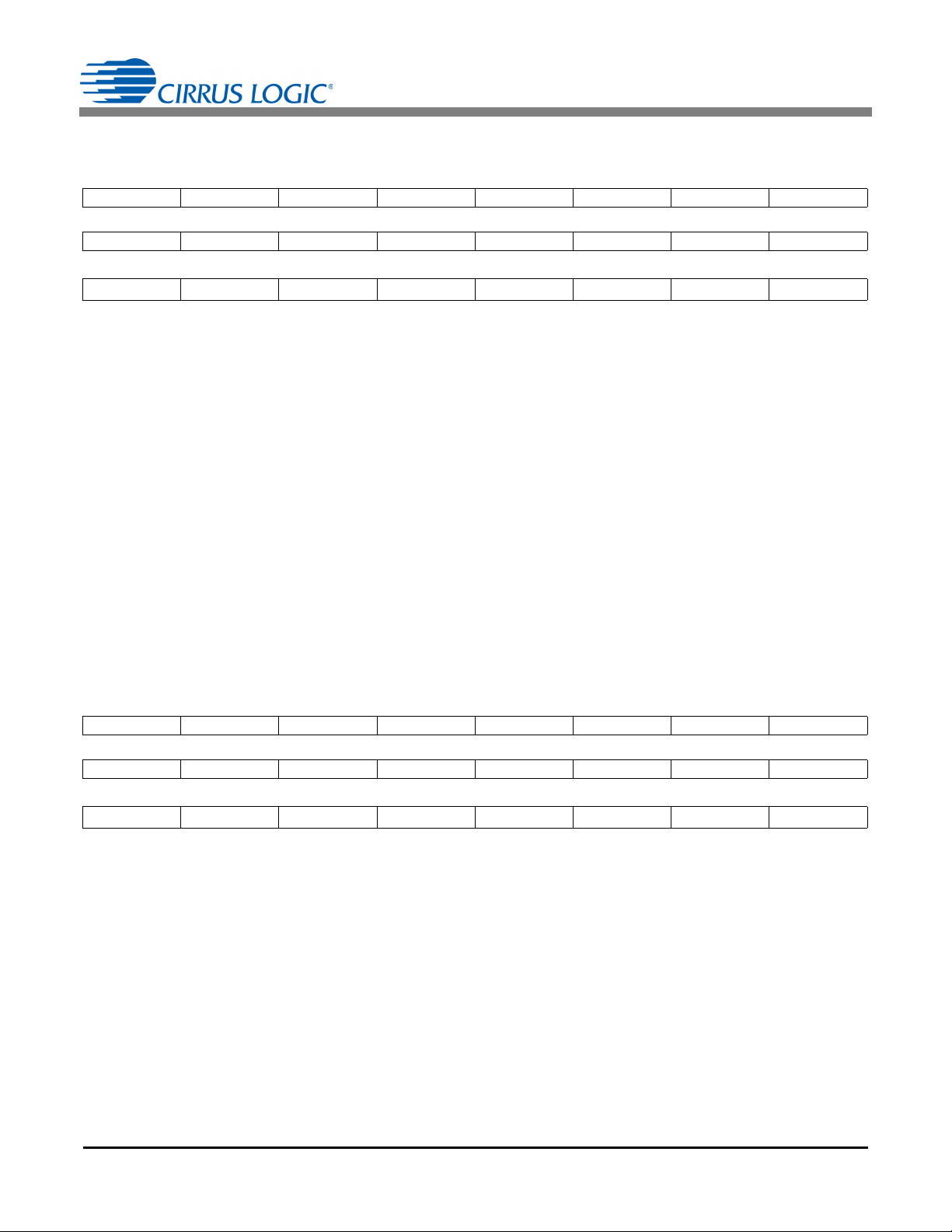
CS5484
6.6.8 Pulse Output Control (PulseCtrl) – Page 0, Address 9
23 22 21 20 19 18 17 16
--------
15 14 13 12 11 10 9 8
EPG4IN[3] EPG4IN[2] EPG4IN[1] EPG4IN[0] EPG3IN[3] EPG3IN[2] EPG3IN[1] EPG3IN[0]
76543210
EPG2IN[3] EPG2IN[2] EPG2IN[1] EPG2IN[0] EPG1IN[3] EPG1IN[2] EPG1IN[1] EPG1IN[0]
Default = 0x00 0000
This register controls the input to the energy pulse generation block (EPGx).
[23:16] Reserved.
EPGxIN[3:0] Selects the input to the energy pulse generation block (EPGx).
0000 = P1
0001 = P2
0010 = P
0011 = Q1
0100 = Q2
0101 = Q
0110 = S1
0111 = S2
1000 = S
1001 = Unused
...
1111 = Unused
AVG
AVG
SUM
AVG
AVG
SUM
SUM
(Default)
6.6.9 Register Lock Control (RegLock) – Page 0, Address 34
23 22 21 20 19 18 17 16
--------
15 14 13 12 11 10 9 8
- - - DSP_LCK[4] DSP_LCK[3] DSP_LCK[2] DSP_LCK[1] DSP_LCK[0]
76543210
- - - HOST_LCK[4] HOST_LCK[3] HOST_LCK[2] HOST_LCK[1] HOST_LCK[0]
Default = 0x00 0000
[23:13] Reserved.
DSP_LCK[4:0] DSP_LCK[4:0] = 0x16 sets the DSP lockable registers to be write protected from the
CS5484 internal calculation engine. Writing 0x09 unlocks the registers.
[7:5] Reserved.
HOST_LCK[4:0] HOST_LCK[4:0] = 0x16 sets all the registers except RegLock, Status0, Status1, and
Status2 to be write protected from the serial interface. Writing 0x09 unlocks the registers.
42 DS981F3
Page 43

CS5484
6.6.10 Phase Sequence Detection and Control (PSDC) – Page 0, Address 48
23 22 21 20 19 18 17 16
DONE PSCNT[6] PSCNT[5] PSCNT[4] PSCNT[3] PSCNT[2] PSCNT[1] PSCNT[0]
15 14 13 12 11 10 9 8
------ --
765432 10
- - DIR CODE[4] CODE[3] CODE[2] CODE[1] CODE[0]
Default = 0x00 0000
DONE Indicates valid count values reside in PSCNT[6:0].
0 = Invalid values in PSCNT[6:0]. (Default)
1 = Valid values in PSCNT[6:0].
PSCNT[6:0] Registers the number of OWR samples from the start time to the time when the next
zero crossing is detected.
[15:6] Reserved.
DIR Set the zero-crossing edge direction which will stop PSCNT count.
0 = Stop count at negative to positive zero-crossing - Rising Edge. (Default)
1 = Stop count at positive to negative zero-crossing - Falling Edge.
CODE[4:0] Write 10110 to this location to enable the phase sequence detection.
6.6.11 Checksum of Critical Registers (RegChk) – Page 16, Address 1
MSB LSB
23
2
22
2
21
2
20
2
19
2
18
2
17
2
16
2
.....
Default = 0x00 0000
This register contains the checksum of critical registers.
6
2
5
2
4
2
3
2
2
2
1
2
0
2
DS981F3 43
Page 44

CS5484
6.6.12 Interrupt Status (Status0) – Page 0, Address 23
23 22 21 20 19 18 17 16
DRDY CRDY WOF - - MIPS V2SWELL V1SWELL
15 14 13 12 11 10 9 8
P2OR P1OR I2OR I1OR V2OR V1OR I2OC I1OC
76543 2 10
V2SAG V1SAG TUP FUP IC RX_CSUM_ERR -
Default = 0x80 0000
The Status0 register indicates a variety of conditions within the chip.
Writing a one to a Status0 register bit will clear that bit. Writing a zero to any bit has no effect.
DRDY Data Ready.
During conversion, this bit indicates that low-rate results have been updated.
It indicates completion of other host instruction and the reset sequence.
CRDY Conversion Ready.
Indicates that sample rate (output word rate) results have been updated.
WOF Watchdog timer overflow.
RX_TO
[20:19] Reserved.
MIPS MIPS overflow.
Sets when the calculation engine has not completed processing a sample before the
next one arrives.
V2SWELL(V1SWELL) Voltage channel 2 (voltage channel 1) swell event detected.
P2OR (P1OR) Power out of range.
Sets when the measured power would cause the P2 (P1) register to overflow.
I2OR (I1OR) Current out of range.
Set when the measured current would cause the I2 (I1) register to overflow.
V2OR (V1OR) Voltage out of range.
Set when the measured voltage would cause the V2 (V1) register to overflow.
I2OC (I1OC) I2 (I1) overcurrent.
V2SAG (V1SAG) Voltage channel 2 (voltage channel 1) sag event detected.
TUP Temperature updated.
Indicates when the Temperature register (T) has been updated.
FUP Frequency updated.
Indicates the Epsilon register has been updated.
IC Invalid command has been received.
RX_CSUM_ERR Received data checksum error.
Sets to one automatically if checksum error is detected on serial port received data.
[1] Reserved.
RX_TO SDI/RX time out.
Sets to one automatically when SDI/RX time out occurs.
44 DS981F3
Page 45
CS5484
6.6.13 Interrupt Mask (Mask) – Page 0, Address 3
23 22 21 20 19 18 17 16
DRDY CRDY WOF - - MIPS V2SWELL V1SWELL
15 14 13 12 11 10 9 8
P2OR P1OR I2OR I1OR V2OR V1OR I2OC I1OC
76543 2 10
V2SAG V1SAG TUP FUP IC RX_CSUM_ERR -
Default = 0x00 0000
The Mask register is used to control the activation of the INT
the corresponding Status0 register bit to activate the INT
pin. Writing a '1' to a Mask register bit will allow
pin when set.
[23:0] Enable / disable (mask) interrupts.
0 = Interrupt disabled (Default)
1 = Interrupt enabled
6.6.14 Chip Status 1 (Status1) – Page 0, Address 24
23 22 21 20 19 18 17 16
--------
15 14 13 12 11 10 9 8
LCOM[7] LCOM[6] LCOM[5] LCOM[4] LCOM[3] LCOM[2] LCOM[1] LCOM[0]
76543210
- - - - V2OD V1OD I2OD I1OD
RX_TO
Default = 0x80 1800
This register indicates a variety of conditions within the chip.
[23:16] Reserved.
LCOM[7:0] Indicates the value of the last serial command executed.
V2OD (V1OD) Modulator oscillation has been detected in the voltage2 (voltage1) ADC.
I2OD (I1OD) Modulator oscillation has been detected in the current2 (current1) ADC.
DS981F3 45
Page 46
CS5484
6.6.15 Chip Status 2 (Status2) – Page 0, Address 25
23 22 21 20 19 18 17 16
--------
15 14 13 12 11 10 9 8
--------
76543210
- - QSUM_SIGN Q2_SIGN Q1_SIGN PSUM_SIGN P2_SIGN P1_SIGN
Default = 0x00 0000
This register indicates a variety of conditions within the chip.
[23:6] Reserved.
QSUM_SIGN Indicates the sign of the value contained in Q
0 = positive value
1 = negative value
Q2_SIGN Indicates the sign of the value contained in Q2
0 = positive value
1 = negative value
Q1_SIGN Indicates the sign of the value contained in Q1
0 = positive value
1 = negative value
PSUM_SIGN Indicates the sign of the value contained in P
0 = positive value
1 = negative value
P2_SIGN Indicates the sign of the value contained in P2
0 = positive value
1 = negative value
P1_SIGN Indicates the sign of the value contained in P1
0 = positive value
1 = negative value
SUM
AVG
AVG
SUM
AVG
AVG
.
.
.
.
.
.
46 DS981F3
Page 47

CS5484
6.6.16 Line to Sample Frequency Ratio (Epsilon) – Page 16, Address 49
MSB LSB
-(20)2-12
-2
Default = 0x01 999A (0.0125 or 50Hz/ 4.0kHz)
Epsilon is the ratio of the input line frequency to the OWR.
It can either be written by the application program or calculated automatically from the line frequency (from
the voltage channel 1 input) using the AFC bit in the Config2 register. It is a two's complement value in the
range of -1.0 value 1.0, with the binary point to the right of the MSB. Negative values are not used.
-3
2
-4
2
-5
2
-6
2
-7
2
.....
-17
2
-18
2
-19
2
-20
2
-21
2
-22
2
-23
2
6.6.17 No-Load Threshold (Load
) – Page 16, Address 58
MIN
MSB LSB
-(20)2-12
-2
-3
2
-4
2
-5
2
-6
2
-7
2
.....
-17
2
-18
2
-19
2
-20
2
-21
2
-22
2
Default = 0x00 0000
Load
When the magnitudes of P
the magnitude of S
Load
is used to set the no-load threshold for the anti-creep function.
MIN
and Q
SUM
is less than Load
SUM
is a two’s complement value in the range of -1.0 value 1.0, with the binary point to the right of the
MIN
are less than Load
SUM
, S
MIN
is forced to zero.
SUM
MIN
, P
SUM
and Q
are forced to zero. When
SUM
MSB. Negative values are not used.
6.6.18 Sample Count (SampleCount) – Page 16, Address 51
MSB LSB
0
22
2
Default = 0x00 0FA0 (4000)
Determines the number of OWR samples to use in calculating low-rate results.
SampleCount (N) is an integer in the range of 100 to 8,388,607. Values less than 100 should not be used.
21
2
20
2
19
2
18
2
17
2
16
2
.....
6
2
5
2
4
2
3
2
2
2
1
2
-23
2
0
2
6.6.19 Cycle Count (CycleCount) – Page 18, Address 62
MSB LSB
0
22
2
Default = 0x00 0064 (100)
Determines the number of half-line cycles to use in calculating low-rate results when the CS5484 is in Line-cycle Synchronized Averaging mode.
CycleCount is an integer in the range of 1 to 8,388,607. Zero should not be used.
DS981F3 47
21
2
20
2
19
2
18
2
17
2
16
2
.....
6
2
5
2
4
2
3
2
2
2
1
2
0
2
Page 48

CS5484
6.6.20 Filter Settling Time for Conversion Startup (T
SETTLE
) – Page 16, Address 57
MSB LSB
23
2
22
2
21
2
20
2
19
2
18
2
17
2
16
2
.....
6
2
5
2
4
2
3
2
2
2
1
2
Default = 0x00 001E (30)
Sets the number of OWR samples that will be used to allow filters to settle at the beginning of Conversion and
Calibration commands.
This is an integer in the range of 0 to 16,777,215 samples.
6.6.21 System Gain (Sys
MSB LSB
-(21)202
-1
-2
2
) – Page 16, Address 60
GAIN
-3
2
-4
2
-5
2
-6
2
.....
-16
2
-17
2
-18
2
-19
2
-20
2
-21
2
Default = 0x50 0000 (1.25)
System Gain (Sys
By default, Sys
GAIN
) is applied to all channels.
GAIN
= 1.25 but can be finely adjusted to compensate for voltage reference error. It is a two's
complement value in the range of -2.0 value 2.0, with the binary point to the right of the second MSB. Values should be kept within 5% of 1.25.
0
2
-22
2
6.6.22 Rogowski Coil Integrator Gain (Int
) – Page 18, Address 43
GAIN
MSB LSB
-(20)2-12
-2
-3
2
-4
2
-5
2
-6
2
-7
2
.....
-17
2
-18
2
-19
2
-20
2
-21
2
-22
2
Default = 0x14 3958
Gain for the Rogowski coil integrator. This must be programmed accordingly for 50Hz and 60Hz (0.158 for
50Hz, 0.1875 for 60 Hz).
This is a two's complement value in the range of -1.0 value 1.0, with the binary point to the right of the MSB.
Negative values are not used.
6.6.23 System Time (Time) – Page 16, Address 61
MSB LSB
23
2
22
2
21
2
20
2
19
2
18
2
17
2
16
2
.....
6
2
5
2
4
2
3
2
2
2
1
2
Default = 0x00 0000
System Time (Time) is measured in OWR samples.
This is an unsigned integer in the range of 0 to 16,777,215 samples. At OWR = 4.0 kHz, OWR will overflow
every 1 hour, 9 minutes, 54 seconds. Time can be used by the application to manage real-time events.
-23
2
0
2
48 DS981F3
Page 49

CS5484
6.6.24 Voltage 1 Sag Duration (V1Sag
) – Page 17, Address 0
DUR
MSB LSB
0
22
2
21
2
20
2
19
2
18
2
17
2
16
2
.....
6
2
5
2
4
2
3
2
2
2
1
2
Default = 0x00 0000
Voltage sag duration, V1Sag
, determines the count of OWR samples utilized to determine a sag event.
DUR
These are integers in the range of 0 to 8,388,607 samples. A value of zero disables the feature.
6.6.25 Voltage 1 Sag Level (V1Sag
MSB LSB
-(20)2-12
-2
-3
2
-4
2
-5
2
) – Page 17, Address 1
LEVEL
-6
2
-7
2
.....
-17
2
-18
2
-19
2
-20
2
-21
2
-22
2
Default = 0x00 0000
Voltage sag level, V1Sag
, establishes an input level below which a sag event is triggered.
LEVEL
This is a two's complement value in the range of -1.0 value 1.0, with the binary point to the right of the MSB.
Negative values are not used.
6.6.26 Current 1 Overcurrent Duration (I1Over
) – Page 17, Address 4
DUR
0
2
-23
2
MSB LSB
0
22
2
21
2
20
2
19
2
18
2
17
2
16
2
.....
6
2
5
2
4
2
3
2
2
2
1
2
Default = 0x00 0000
Overcurrent duration, I1Over
, determines the count of OWR samples utilized to determine an overcurrent
DUR
event.
These are integers in the range of 0 to 8,388,607 samples. A value of zero disables the feature.
6.6.27 Current 1 Overcurrent Level (I1Over
MSB LSB
-(20)2-12
-2
-3
2
-4
2
-5
2
-6
2
) – Page 17, Address 5
LEVEL
-7
2
.....
-17
2
-18
2
-19
2
-20
2
-21
2
-22
2
Default = 0x7F FFFF
Overcurrent level, I1Over
, establishes an input level above which an overcurrent event is triggered.
LEVEL
This is a two's complement value in the range of -1.0 value 1.0, with the binary point to the right of the MSB.
Negative values are not used.
0
2
-23
2
DS981F3 49
Page 50

CS5484
6.6.28 Voltage 2 Sag Duration (V2Sag
) – Page 17, Address 8
DUR
MSB LSB
0
22
2
21
2
20
2
19
2
18
2
17
2
16
2
.....
6
2
5
2
4
2
3
2
2
2
1
2
Default = 0x00 0000
Voltage sag duration, V2Sag
, determines the count of OWR samples utilized to determine a sag event.
DUR
These are integers in the range of 0 to 8,388,607 samples. A value of zero disables the feature.
6.6.29 Voltage 2 Sag Level (V2Sag
MSB LSB
-(20)2-12
-2
-3
2
-4
2
-5
2
) – Page 17, Address 9
LEVEL
-6
2
-7
2
.....
-17
2
-18
2
-19
2
-20
2
-21
2
-22
2
Default = 0x00 0000
Voltage sag level, V2Sag
, establishes an input level below which a sag event is triggered.
LEVEL
This is a two's complement value in the range of -1.0 value 1.0, with the binary point to the right of the MSB.
Negative values are not used.
6.6.30 Current 2 Overcurrent Duration (I2Over
) – Page 17, Address 12
DUR
0
2
-23
2
MSB LSB
0
22
2
21
2
20
2
19
2
18
2
17
2
16
2
.....
6
2
5
2
4
2
3
2
2
2
1
2
Default = 0 x00 0000
Overcurrent duration, I2Over
, determines the count of OWR samples utilized to determine an overcurrent
DUR
event.
These are integers in the range of 0 to 8,388,607 samples. A value of zero disables the feature.
6.6.31 Current 2 Overcurrent Level (I2Over
MSB LSB
-(20)2-12
-2
-3
2
-4
2
-5
2
-6
2
) – Page 17, Address 13
LEVEL
-7
2
.....
-17
2
-18
2
-19
2
-20
2
-21
2
-22
2
Default = 0x7F FFFF
Overcurrent level, I2Over
, establishes an input level above which an overcurrent event is triggered.
LEVEL
This is a two's complement value in the range of -1.0value1.0, with the binary point to the right of the MSB.
Negative values are not used.
0
2
-23
2
50 DS981F3
Page 51

CS5484
6.6.32 Voltage 1 Swell Duration (V1Swell
) – Page 18, Address 46
DUR
MSB LSB
0
22
2
21
2
20
2
19
2
18
2
17
2
16
2
.....
6
2
5
2
4
2
3
2
2
2
1
2
Default = 0x00 0000
Voltage swell duration, V1Swell
, determines the count of OWR samples utilized to determine a swell
DUR
event.
These are integers in the range of 0 to 8,388,607 samples. A value of zero disables the feature.
6.6.33 Voltage 1 Swell Level (V1Swell
MSB LSB
-(20)2-12
-2
-3
2
-4
2
-5
2
) – Page 18, Address 47
LEVEL
-6
2
-7
2
.....
-17
2
-18
2
-19
2
-20
2
-21
2
-22
2
Default = 0x7F FFFF
Voltage swell level, V1Swell
, establishes an input level above which a swell event is triggered.
LEVEL
This is a two's complement value in the range of -1.0value1.0, with the binary point to the right of the MSB.
Negative values are not used.
0
2
-23
2
6.6.34 Voltage 2 Swell Duration (V2Swell
) – Page 18, Address 50
DUR
MSB LSB
0
22
2
21
2
20
2
19
2
18
2
17
2
16
2
.....
6
2
5
2
4
2
3
2
2
2
1
2
Default = 0x00 0000
Voltage swell duration, V2Swell
, determines the count of OWR samples utilized to determine a swell
DUR
event.
These are integers in the range of 0 to 8,388,607 samples. A value of zero disables the feature.
6.6.35 Voltage 2 Swell Level (V2Swell
LEVEL
MSB LSB
-(20)2-12
-2
-3
2
-4
2
-5
2
) – Page 18, Address 51
-6
2
-7
.....
2
2
-17
-18
2
-19
2
-20
2
-21
2
-22
2
Default = 0x7F FFFF
Voltage swell level, V2Swell
, establishes an input level above which a swell event is triggered.
LEVEL
This is a two's complement value in the range of -1.0 value 1.0, with the binary point to the right of the MSB.
Negative values are not used.
0
2
-23
2
DS981F3 51
Page 52

CS5484
6.6.36 Instantaneous Current 1 (I1) – Page 16, Address 2
MSB LSB
-(20)2-12
-2
Default = 0x00 0000
I1 contains instantaneous current measurements for current channel 1.
This is a two's complement value in the range of -1.0value1.0, with the binary point to the right of the MSB.
6.6.37 Instantaneous Voltage 1 (V1) – Page 16, Address 3
MSB LSB
-(20)2-12
Default = 0x00 0000
V1 contains instantaneous voltage measurements for voltage channel 1.
This is a two's complement value in the range of -1.0 value 1.0, with the binary point to the right of the MSB.
-2
-3
2
-3
2
-4
2
-4
2
-5
2
-5
2
-6
2
-6
2
-7
2
2
.....
-7
.....
-17
2
-17
2
-18
2
-18
2
-19
2
-19
2
-20
2
-20
2
-21
2
-21
2
-22
2
-22
2
-23
2
-23
2
6.6.38 Instantaneous Active Power 1 (P1) – Page 16, Address 4
MSB LSB
-(20)2-12
-2
Default = 0x00 0000
P1 contains instantaneous power measurements for current and voltage channels 1.
Values in registers I1 and V1 are multiplied to generate this value. This is a two's complement value in the
range of -1.0 value 1.0, with the binary point to the right of the MSB.
6.6.39 Active Power 1 (P1
MSB LSB
-(20)2-12
Default = 0x00 0000
Instantaneous power is averaged over each low-rate interval (SampleCount samples) and then added with
power offset (P
This is a two's complement value in the range of -1.0 value 1.0, with the binary point to the right of the MSB.
-2
OFF
-3
2
-3
2
2
AVG
2
-4
-4
-5
2
) – Page 16, Address 5
-5
2
) to compute active power (P
-6
2
-6
2
2
2
-7
-7
AVG
.....
.....
-17
2
-17
2
-18
2
-18
2
-19
2
-19
2
-20
2
-20
2
-21
2
-21
2
-22
2
-22
2
).
-23
2
-23
2
52 DS981F3
Page 53

CS5484
6.6.40 RMS Current 1 (I1
) – Page 16, Address 6
RMS
MSB LSB
-1
2
-2
2
-3
2
-4
2
-5
2
-6
2
-7
2
-8
2
.....
-18
2
-19
2
-20
2
-21
2
-22
2
-23
2
Default = 0x00 0000
I1
contains the root mean square (RMS) values of I1, calculated during each low-rate interval.
RMS
This is an unsigned value in the range of 0 value 1.0, with the binary point to the left of the MSB.
6.6.41 RMS Voltage 1 (V1
MSB LSB
-1
2
-2
2
-3
2
-4
2
) – Page 16, Address 7
RMS
-5
2
-6
2
-7
2
-8
2
.....
-18
2
-19
2
-20
2
-21
2
-22
2
-23
2
Default = 0x00 0000
V1
contains the root mean square (RMS) value of V1, calculated during each low-rate interval.
RMS
This is an unsigned value in the range of 0 value 1.0, with the binary point to the left of the MSB.
6.6.42 Instantaneous Current 2 (I2) – Page 16, Address 8
-24
2
-24
2
MSB LSB
-(20)2-12
-2
-3
2
-4
2
-5
2
-6
2
-7
2
.....
-17
2
-18
2
-19
2
-20
2
-21
2
-22
2
Default = 0x00 0000
I2 contains instantaneous current measurements for current channel 2.
This is a two's complement value in the range of -1.0 value 1.0, with the binary point to the right of the MSB.
6.6.43 Instantaneous Voltage 2 (V2) – Page 16, Address 9
MSB LSB
0
)2-12
-(2
Default = 0x00 0000
V2 contains instantaneous voltage measurements for voltage channel 2.
This is a two's complement value in the range of -1.0 value 1.0, with the binary point to the right of the MSB.
-2
-3
2
-4
2
-5
2
-6
2
-7
2
.....
-17
2
-18
2
-19
2
-20
2
-21
2
-22
2
-23
2
-23
2
DS981F3 53
Page 54

CS5484
6.6.44 Instantaneous Active Power 2 (P2) – Page 16, Address 10
MSB LSB
-(20)2-12
-2
Default = 0x00 0000
P2 contains instantaneous power measurements for current and voltage channels 2.
Values in registers I2 and V2 are multiplied to generate this value. This is a two's complement value in the
range of -1.0 value 1.0, with the binary point to the right of the MSB.
-3
2
-4
2
-5
2
-6
2
-7
2
.....
-17
2
-18
2
-19
2
-20
2
-21
2
-22
2
-23
2
6.6.45 Active Power 2 (P2
) – Page 16, Address 11
AVG
MSB LSB
-(20)2-12
-2
-3
2
-4
2
-5
2
-6
2
-7
2
.....
-17
2
-18
2
-19
2
-20
2
-21
2
-22
2
Default = 0x00 0000
Instantaneous power is averaged over each low-rate interval (SampleCount samples) to compute active power (P2
AVG
).
This is a two's complement value in the range of -1.0 value 1.0, with the binary point to the right of the MSB.
6.6.46 RMS Current 2 (I2
MSB LSB
-1
2
-2
2
-3
2
-4
2
) – Page 16, Address 12
RMS
-5
2
-6
2
-7
2
-8
2
.....
-18
2
-19
2
-20
2
-21
2
-22
2
-23
2
Default = 0x00 0000
I2
contains the root mean square (RMS) value of I2, calculated during each low-rate interval.
RMS
This is an unsigned value in the range of 0 value 1.0, with the binary point to the left of the MSB.
6.6.47 RMS Voltage 2 (V2
) – Page 16, Address 13
RMS
-23
2
-24
2
MSB LSB
-1
2
-2
2
-3
2
-4
2
-5
2
-6
2
-7
2
-8
2
.....
-18
2
-19
2
-20
2
-21
2
-22
2
-23
2
-24
2
Default = 0x00 0000
V2
contains the root mean square (RMS) value of V2, calculated during each low-rate interval.
RMS
This is an unsigned value in the range of 0 value 1.0, with the binary point to the left of the MSB.
54 DS981F3
Page 55

CS5484
6.6.48 Reactive Power 1 (Q1
) – Page 16, Address 14
Avg
MSB LSB
-(20)2-12
-2
-3
2
-4
2
-5
2
-6
2
-7
2
.....
-17
2
-18
2
-19
2
-20
2
-21
2
-22
2
Default = 0x00 0000
Reactive power 1 (Q1
by Q
OFF
.
) is Q1 averaged over each low-rate interval (SampleCount samples) and corrected
AVG
This is a two's complement value in the range of -1.0 value 1.0, with the binary point to the right of the MSB.
6.6.49 Instantaneous Quadrature Power 1 (Q1) – Page 16, Address 15
MSB LSB
-(20)2-12
-2
Default = 0x00 0000
Instantaneous quadrature power, Q1, the product of V1 shifted 90 degrees and I1.
This is a two's complement value in the range of -1.0 value 1.0, with the binary point to the right of the MSB.
6.6.50 Reactive Power 2 (Q2
-3
2
-4
2
-5
2
) – Page 16, Address 16
Avg
-6
2
-7
2
.....
-17
2
-18
2
-19
2
-20
2
-21
2
-22
2
-23
2
-23
2
MSB LSB
-(20)2-12
-2
-3
2
-4
2
-5
2
-6
2
-7
2
.....
-17
2
-18
2
-19
2
-20
2
-21
2
-22
2
Default = 0x00 0000
Reactive power 2 (Q2
) is Q2 averaged over each low-rate interval (SampleCount samples).
AVG
This is a two's complement value in the range of -1.0 value 1.0, with the binary point to the right of the MSB.
6.6.51 Instantaneous Quadrature Power 2 (Q2) – Page 16, Address 17
MSB LSB
-(20)2-12
-2
Default = 0x00 0000
Instantaneous quadrature power, Q2, the product of V2 shifted 90 degrees and I2.
This is a two's complement value in the range of -1.0 value 1.0, with the binary point to the right of the MSB.
-3
2
-4
2
-5
2
-6
2
-7
2
.....
-17
2
-18
2
-19
2
-20
2
-21
2
-22
2
-23
2
-23
2
DS981F3 55
Page 56

CS5484
6.6.52 Peak Current 1 (I1
) – Page 0, Address 37
PEAK
MSB LSB
-(20)2-12
-2
-3
2
-4
2
-5
2
-6
2
-7
2
.....
-17
2
-18
2
-19
2
-20
2
-21
2
-22
2
Default = 0x00 0000
Peak current1 (I1
) contains the value of the instantaneous current 1 sample with the greatest magnitude
PEAK
detected during the last low-rate interval.
This is a two's complement value in the range of -1.0 value 1.0, with the binary point to the right of the MSB.
6.6.53 Peak Voltage 1 (V1
MSB LSB
-(20)2-12
-2
-3
2
) – Page 0, Address 36
PEAK
-4
2
-5
2
-6
2
-7
2
.....
-17
2
-18
2
-19
2
-20
2
-21
2
-22
2
Default = 0x00 0000
Peak voltage 1 (V1
) contains the value of the instantaneous voltage 1 sample with the greatest magni-
PEAK
tude detected during the last low-rate interval.
This is a two's complement value in the range of -1.0 value 1.0, with the binary point to the right of the MSB.
-23
2
-23
2
6.6.54 Apparent Power 1 (S1) – Page 16, Address 20
MSB LSB
0
-1
2
-2
2
-3
2
-4
2
-5
2
-6
2
-7
2
.....
-17
2
-18
2
-19
2
-20
2
-21
2
-22
2
Default = 0x00 0000
Apparent power 1 (S1) is the product of V1
RMS
and I1
or SQRT(P1
RMS
AVG
2
+ Q1
AVG
2
).
This is an unsigned value in the range of 0 value 1.0, with the binary point to the right of the MSB.
6.6.55 Power Factor 1 (PF1) – Page 16, Address 21
MSB LSB
-(20)2-12
-2
Default = 0x00 0000
Power factor 1 (PF1) is calculated by dividing active power 1 (P1
The sign is determined by the active power (P1
This is a two's complement value in the range of -1.0 value 1.0, with the binary point to the right of the MSB.
-3
2
-4
2
-5
2
-6
2
2
-7
AVG
.....
) sign.
-17
2
AVG
-18
2
-19
2
-20
2
) by apparent power 1 (S1).
-21
2
-22
2
-23
2
-23
2
56 DS981F3
Page 57

CS5484
6.6.56 Peak Current 2 (I2
) – Page 0, Address 39
PEAK
MSB LSB
-(20)2-12
-2
-3
2
-4
2
-5
2
-6
2
-7
2
.....
-17
2
-18
2
-19
2
-20
2
-21
2
-22
2
Default = 0x00 0000
Peak current, I2
, contains the value of the instantaneous current 2 sample with the greatest magnitude
PEAK
detected during the last low-rate interval.
This is a two's complement value in the range of -1.0value1.0, with the binary point to the right of the MSB.
6.6.57 Peak Voltage 2 (V2
MSB LSB
-(20)2-12
-2
-3
2
) – Page 0, Address 38
PEAK
-4
2
-5
2
-6
2
-7
2
.....
-17
2
-18
2
-19
2
-20
2
-21
2
-22
2
Default = 0x00 0000
Peak voltage, V2
, contains the value of the instantaneous voltage 2 sample with the greatest magnitude
PEAK
detected during the last low-rate interval.
This is a two's complement value in the range of -1.0value1.0, with the binary point to the right of the MSB.
-23
2
-23
2
6.6.58 Apparent Power 2 (S2) – Page 16, Address 24
MSB LSB
0
-1
2
-2
2
-3
2
-4
2
-5
2
-6
2
-7
2
.....
-17
2
-18
2
-19
2
-20
2
-21
2
-22
2
Default = 0x00 0000
Apparent power 2 (S2) is the product of V2
RMS
and I2
or SQRT(P2
RMS
AVG
2
+ Q2
AVG
2
).
This is an unsigned value in the range of 0 value 1.0, with the binary point to the right of the MSB.
6.6.59 Power Factor 2 (PF2) – Page 16, Address 25
MSB LSB
-(20)2-12
-2
Default = 0x00 0000
Power factor 2 (PF2) is calculated by dividing active power 2 (P2
The sign is determined by the active power (P2
This is a two's complement value in the range of -1.0 value1.0, with the binary point to the right of the MSB.
-3
2
-4
2
-5
2
-6
2
2
-7
AVG
.....
) sign.
-17
2
AVG
-18
2
-19
2
-20
2
) by apparent power 2 (S2).
-21
2
-22
2
-23
2
-23
2
DS981F3 57
Page 58

CS5484
6.6.60 Temperature (T) – Page 16, Address 27
MSB LSB
-(27)262
5
Default = 0x00 0000
T contains results from the on-chip temperature measurement.
By default, T uses the Celsius scale and is a two's complement value in the range of -128.0value128.0
(°C), with the binary point to the right of bit 16.
4
2
3
2
2
2
1
2
0
.....
2
-10
2
-11
2
-12
2
-13
2
-14
2
-15
2
-16
2
T can be rescaled by the application using the T
6.6.61 Total Active Power (P
) – Page 16, Address 29
SUM
GAIN
and T
registers.
OFF
MSB LSB
-(20)2-12
-2
-3
2
-4
2
-5
2
-6
2
-7
2
.....
-17
2
-18
2
-19
2
-20
2
-21
2
-22
2
Default = 0x00 0000
P
SUM
=P1
AVG
+P2
AVG
This is a two's complement value in the range of -1.0value1.0, with the binary point to the right of the MSB.
6.6.62 Total Apparent Power (S
MSB LSB
0
-1
2
-2
2
-3
2
-4
2
) – Page 16, Address 30
SUM
-5
2
-6
2
-7
2
.....
-17
2
-18
2
-19
2
-20
2
-21
2
-22
2
Default = 0x00 0000
S
=S1+S2
SUM
This is an unsigned value in the range of 0.0 value1.0, with the binary point to the right of the MSB.
-23
2
-23
2
6.6.63 Total Reactive Power (Q
) – Page 16, Address 31
SUM
MSB LSB
-(20)2-12
-2
-3
2
-4
2
-5
2
-6
2
-7
2
.....
-17
2
-18
2
-19
2
-20
2
-21
2
-22
2
-23
2
Default = 0x00 0000
Q
SUM
=Q1
AVG
+Q2
AVG
This is a two's complement value in the range of -1.0 value1.0, with the binary point to the right of the MSB.
58 DS981F3
Page 59

CS5484
6.6.64 DC Offset for Current (I1
DCOFF
, I2
DCOFF
) – Page 16, Address 32, 39
MSB LSB
-(20)2-12
-2
-3
2
-4
2
-5
2
-6
2
-7
2
.....
-17
2
-18
2
-19
2
-20
2
-21
2
-22
2
Default = 0x00 0000
DC offset registers I1
DCOFF
and I2
are initialized to zero on reset. D uring DC offset calibration, selected
DCOFF
registers are written with the inverse of the DC offset measured. The application program can also write the
DC offset register values. These are two's complement values in the range of -1.0 value 1.0, with the binary
point to the right of the MSB.
6.6.65 DC Offset for Voltage (V1
DCOFF
MSB LSB
0
)2-12
-(2
-2
-3
2
-4
2
, V2
DCOFF
-5
2
-6
2
) – Page 16, Address 34, 41
-7
2
.....
-17
2
-18
2
-19
2
-20
2
-21
2
-22
2
Default = 0x00 0000
DC offset registers V1
DCOFF
and V2
are initialized to zero on reset. During DC offset calibration, select-
DCOFF
ed registers are written with the inverse of the DC offset measured. The application program can also write
the DC offset register values. These are two's complement values in the range of -1.0 value 1.0, with the
binary point to the right of the MSB.
6.6.66 Gain for Current (I1
GAIN
, I2
) – Page 16, Address 33, 40
GAIN
-23
2
-23
2
MSB LSB
1
2
0
2
-1
2
-2
2
-3
2
-4
2
-5
2
-6
2
.....
-16
2
-17
2
-18
2
-19
2
-20
2
-21
2
Default = 0x40 0000 (1.0)
Gain registers I1
GAIN
and I2
are initialized to 1.0 on reset. During gain calibration, selected register are
GAIN
written with the multiplicative inverse of the gain measured. These are unsigned fixed-point values in the
range of 0 value4.0, with the binary point to the right of the second MSB.
6.6.67 Gain for Voltage (V1
MSB LSB
1
2
0
2
-1
2
-2
2
GAIN
-3
2
, V2
2
GAIN
-4
) – Page 16, Address 35, 42
-5
2
-6
2
.....
-16
2
-17
2
-18
2
-19
2
-20
2
-21
2
Default = 0x40 0000 (1.0)
Gain registers V1
GAIN
and V2
are initialized to 1.0 on reset. During gain calibration, selected registers are
GAIN
written with the multiplicative inverse of the gain measured. These are unsigned fixed-point values in the
range of 0 value4.0, with the binary point to the right of the second MSB.
-22
2
-22
2
DS981F3 59
Page 60

CS5484
6.6.68 Average Active Power Offset (P1
OFF
, P2
) – Page 16, Address 36, 43
OFF
MSB LSB
-(20)2-12
-2
-3
2
-4
2
-5
2
-6
2
-7
2
.....
-17
2
-18
2
-19
2
-20
2
-21
2
-22
2
Default = 0x00 0000
Average Active Power offset P1
OFF
(P2
) is added to averaged power to yield P1
OFF
AVG
(P2
) register re-
AVG
sults. It can be used to reduce systematic energy errors. These are two's complement values in the range of
-1.0 value 1.0, with the binary point to the right of the MSB.
6.6.69 Average Reactive Offset (Q1
MSB LSB
0
-(2
)2-12
-2
-3
2
-4
2
2
OFF
-5
, Q2
-6
2
) – Page 16, Address 38, 45
OFF
-7
2
.....
-17
2
-18
2
-19
2
-20
2
-21
2
-22
2
Default = 0x00 0000
Average Reactive Power offset Q1
OFF
(Q2
) is added to averaged reactive power to yield Q1
OFF
AVG
(Q2
register results. It can be used to reduce systematic energy errors. These are two's complement values in the
range of -1.0 value 1.0, with the binary point to the right of the MSB.
6.6.70 AC Offset for Current (I1
ACOFF
, I2
ACOFF
) – Page 16, Address 37, 44
-23
2
-23
2
AVG
)
MSB LSB
-1
2
-2
2
-3
2
-4
2
-5
2
-6
2
-7
2
-8
2
.....
-18
2
-19
2
-20
2
-21
2
-22
2
-23
2
Default = 0x00 0000
AC offset registers I1
ACOFF
and I2
are initialized to zero on reset. They are used to reduce systematic
ACOFF
errors in the RMS results.These are unsigned values in the range of 0 value 1.0, with the binary point to
the left of the MSB.
6.6.71 Temperature Gain (T
MSB LSB
7
2
6
2
5
2
4
2
) – Page 16, Address 54
GAIN
3
2
2
2
1
2
0
.....
2
-10
2
-11
2
-12
2
-13
2
-14
2
-15
2
Default = 0x 06 B716
Register T
is used to scale the Temperature register (T), and is an unsigned fixed-point value in the range
GAIN
of 0.0value256.0, with the binary point to the right of bit 16.
Register T can be rescaled by the application using the T
GAIN
and T
registers. Refer to section 7.3 Tem-
OFF
perature Sensor Calibration on page 65 for more information.
-24
2
-16
2
60 DS981F3
Page 61

CS5484
6.6.72 Temperature Offset (T
) – Page 16, Address 55
OFF
MSB LSB
-(27)262
5
4
2
3
2
2
2
1
2
0
.....
2
-10
2
-11
2
-12
2
-13
2
-14
2
-15
2
Default = 0x D5 3998
Register T
is used to offset the Temperature register (T), and is a two's complement value in the range of
OFF
-128.0value128.0 (°C), with the binary point to the right of bit 16.
Register T can be rescaled by the application using the T
GAIN
and T
registers. Refer to section 7.3 Tem-
OFF
perature Sensor Calibration on page 65 for more information.
6.6.73 Calibration Scale (Scale) – Page18, Address 63
MSB LSB
-(20)2-12
-2
Default = 0 x4C CCCC (0.6)
The Scale register is used in the gain calibration to set the level of calibrated results of I-channel RMS. During
gain calibration, the Ix
register. This is a two's complement value in the range of -1.0 value 1.0, with the binary point to the right of
the MSB. Negative values are not used.
6.6.74 V-Channel Zero-crossing Threshold (VZX
-3
2
RMS
-4
2
-5
2
-6
2
-7
2
.....
-17
2
-18
2
-19
2
-20
2
-21
2
results register is divided into the Scale register. The quotient is put into the Ix
) – Page 18, Address 58
LEVEL
-22
2
-16
2
-23
2
GAIN
MSB LSB
-(20)2-12
-2
-3
2
-4
2
-5
2
-6
2
-7
2
.....
-17
2
-18
2
-19
2
-20
2
-21
2
-22
2
Default = 0x10 0000 (0.125)
VZX
function. This is a two's complement value in the range of -1.0
is the level that the peak instantaneous voltage must exceed for the zero-crossing detection to
LEVEL
value<1.0, with the binary point to the right of
the MSB. Negative values are not used.
6.6.75 I-Channel Zero-crossing Threshold (IZX
MSB LSB
-(20)2-12
-2
-3
2
-4
2
-5
2
-6
2
) – Page 18, Address 24
LEVEL
-7
2
.....
-17
2
-18
2
-19
2
-20
2
-21
2
-22
2
Default = 0x10 0000 (0.125)
IZX
tion. This is a two's complement value in the range of -1.0
is the level that the peak instantaneous current must exceed for the zero-crossing detection to func-
LEVEL
value<1.0, with the binary point to the right of the
MSB. Negative values are not used.
6.6.76 Zero-crossing Number (ZX
MSB LSB
23
2
22
2
21
2
20
2
19
2
) – Page 0, Address 55
NUM
18
2
17
2
16
2
.....
6
2
5
2
4
2
3
2
2
2
1
2
-23
2
-23
2
0
2
Default = 0x00 0064 (100)
ZX
is the number of zero crossings used for line frequency measurement. It is an integer in the range of
NUM
1 to 8,388,607. Zero should not be used.
DS981F3 61
Page 62

7. SYSTEM CALIBRATION
V
RMS
*
, I
RMS
*
Registers
IN
Modulator Filter
N
* Denotes readable/w ritable register
Ϯ
Applies only to the curr ent path (I1, I2)
N
N
-1
N
DC
RMS
-1
RMS
0.6 ( Scale
*
Ϯ
)
V*, I*, P*, Q
*
Registers
I
GAIN
*
, V
GAIN
*
Registers
I
DCOFF
*
, V
DCOFF
*
Registers
I
ACOFF
*
Ϯ
Register
Figure 23. Calibration Data Flow
Component tolerances, residual ADC offset, and
system noise require a meter that needs to be calibrated
before it meets a specific accuracy requirement. The
CS5484 provides an on-chip calibration algorithm to
operate the system calibration quickly and easily.
Benefiting from the excellent linearity and low noise
level of the CS5484, normally a CS5484 meter only
needs one calibration at a single load point to achieve
accurate measurements over the full load range.
7.1 Calibration in General
The CS5484 provides DC offset and gain calibration
that can be applied to the instantaneous voltage and
current measurements and AC offset calibration, which
can be applied to the voltage and current RMS
calculations.
Since the voltage and current channels have
independent offset and gain registers, offset and gain
calibration can be performed on any channel
independently.
The data flow of the calibration is shown in Figure 23.
Note that in Figure 23 the AC offset registers and gain
registers affect the output results differently than the DC
offset registers. The DC offset and gain values are
applied to the voltage/current signals early in the signal
path; the DC offset register and gain register values
affect all CS5484 results. This is not true for the AC
offset correction. The AC offset registers only affect the
results of the RMS voltage and current calculations.
The CS5484 must be operating in its active state and
ready to accept valid commands. Refer to section 6.1.2
Instructions on page 27 for different calibration
CS5484
commands. The value in the SampleCount register
determines the number (N) of output word rate (OWR)
samples that are averaged during a calibration. The
calibration procedure takes the time of N+T
OWR samples. As N is increased, the calibration takes
more time, but the accuracy of the calibration results
tends to increase.
The DRDY bit in the Status0 register will be set at the
completion of calibration commands. If an overflow
occurs during calibration, other Status0 bits may be set
as well.
7.1.1 Offset Calibration
During offset calibrations, no line voltage or current
should be applied to the meter; the differential signal on
voltage inputs V1IN± (V2IN±) or current inputs IIN1±
(IIN2±) of the CS5484 should be 0V.
7.1.1.1 DC Offset Calibration
The DC offset calibration command measures and
averages DC values read on specified voltage or
current channels at zero input and stores the inverse
result in the associated offset registers. This DC offset
will be added to instantaneous measurements in
subsequent conversions, removing the offset.
The gain register for the channel being calibrated
should be set to 1.0 prior to performing DC offset
calibration.
DC offset calibration is not required if the high-pass filter
is enabled on that channel because the DC component
will be removed by the high-pass filter.*
SETTLE
62 DS981F3
Page 63

CS5484
0xFFFFFF
7.1.1.2 AC Offset Calibration
The AC offset calibration command measures the
residual RMS values on the current channel at zero
input and stores the squared result in the associated AC
offset register. This AC offset will be subtracted from
RMS measurements in subsequent conversions,
removing the AC offset on the associated current
channel.
The AC offset register for the channel being calibrated
should first be cleared prior to performing the
calibration. The high-pass filter should be enabled if AC
offset calibration is used. It is recommended that
T
be set to 2000 ms before performing an AC
SETTLE
offset calibration. Note that the AC offset register holds
the square of RMS value measured during calibration.
Therefore, it can hold a maximum RMS noise
of . This is the maximum RMS noise that AC
offset correction can remove.
7.1.2 Gain Calibration
Prior to executing the gain calibration command, gain
registers for any path to be calibrated (Vx
should be set to 1.0, and T
SETTLE
should be set to
2000 ms. For gain calibration, a reference signal must
be applied to the meter. During gain calibration, the
voltage RMS result register (Vx
and the current RMS result register (Ix
) is divided into 0.6,
RMS
RMS
into the Scale register. The quotient is put into the
associated gain register. The gain calibration algorithm
attempts to adjust the gain register (Vx
such that the voltage RMS result register (Vx
equals 0.6, and the current RMS result register (Ix
equals the Scale register.
Note that for the gain calibration, there are limitations on
choosing the reference level and the Scale register
value. Using a reference or a scale that is too large or
too small can cause register overflow during calibration
or later during normal operation. Either condition can set
Status register bits I1OR (I2OR) V1OR (V2OR). The
maximum value that the gain register can attain is four.
Using inappropriate reference levels or scale values
may also cause the CS5484 to attempt to set the gain
register higher than four, therefore the gain calibration
result will be invalid.
The Scale register is 0.6 by default. The maximum
voltage (U
Volts) and current (I
MAX
MAX
meter should be used as the reference signal level if the
Scale register is 0.6. After gain calibration, 0.6 of the
Vx
RMS
(Ix
) register represents U
RMS
MAX
Amps) for the line voltage (load current); 0.36 of the
Px
AVG
, Qx
, or Sx register represents U
AVG
, Ix
GAIN
GAIN
) is divided
, Ix
GAIN
GAIN
RMS
RMS
Amps) of the
Volts (I
MAX
MAX×IMAX
Watts, Vars, or VAs for the active, reactive, or apparent
power.
If the calibration is performed with U
Amps and I
CAL<IMAX
scaled down to 0.6× I
, the Scale register needs to be
CAL/IMAX
before performing gain
Volts and I
MAX
calibration. After gain calibration, 0.6 of the Vx
register represents U
Ix
register represents I
RMS
0.36 x I
CAL/IMAX
represents U
of the Px
MAXxICAL
Volts, 0.6xI
MAX
AVG
, Qx
CAL/IMAX
Amps, and
CAL
, or Sx register
AVG
Watts, Vars, or VAs.
7.1.3 Calibration Order
1. If the HPF option is enabled, then any DC
component that may be present in the selected
signal channel will be removed, and a DC offset
calibration is not required. However, if the HPF
option is disabled, the DC offset calibration should
be performed.
When using high-pass filters, it is recommended that
the DC offset register for the corresponding channel
be set to zero. Before performing DC offset calibra-
)
tion, the DC offset register should be set to 0, and the
corresponding gain register should be set to 1.
2. If there is an AC offset in the Ix
calculation, the
RMS
AC offset calibration should be performed on the
current channel. Before performing AC offset
calibration, the AC offset register should be set to 0.
It is recommended that T
SETTLE
be set to 2000 ms
before performing an AC offset calibration.
)
3. Perform the gain calibration.
)
4. If an AC offset calibration was performed (step 2),
)
then the AC offset may need to be adjusted to
compensate for the change in gain (step 3). This can
be accomplished by restoring zero to the AC offset
register and then performing an AC offset calibration.
The adjustment could also be done by multiplying
the AC offset register value that was calculated in
step 2 by the gain calculated in step 3 and updating
the AC offset register with the product.
7.2 Phase Compensation
A phase compensation mechanism is provided to adjust
for meter-to-meter variation in signal path delays. Phase
offset between a voltage channel and its corresponding
current channel can be calculated by using the power
factor (PF1, PF2) register after a conversion.
1) Apply a reference voltage and current with a lagging
power factor to the meter. The reference current
waveform should lag the voltage with a 60° phase
shift.
2) Start continuous conversion.
CAL
RMS
of the
DS981F3 63
Page 64
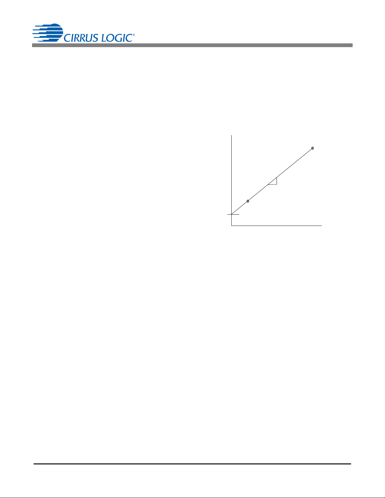
CS5484
ymxb+=
Force Temperature (
°
C)
T Register Value
Y = m • x + b
m
b
T1
T2
T
OFF
b
m
-----
=
T
GAIN
m=
3) Accumulate multiple readings of the PF1 or PF2
register.
4) Calculate the average power factor, PF
5) Calculate phase offset = arccos(PF
avg
.
avg
) - 60°.
6) If the phase offset is negative, then the delay should
be added only to the current channel. Otherwise,
add more delay to the voltage channel than to the
current channel to compensate for a positive phase
offset.
Once the phase offset is known, the CPCCx and FPCCx
bits for that channel are calculated and programmed in
the PC register.
CPCCx bits are used if either:
• The phase offset is more than 1 output word rate
(OWR) sample.
• More delay is needed on the voltage channel.
The compensation resolution is 0.008789° at 50Hz and
0.010547° at 60Hz at an OWR of 4000Hz.
7.3 Temperature Sensor Calibration
Temperature sensor calibration involves the adjustment
of two parameters: temperature gain (T
temperature offset (T
must be set to 1.0 (0x 01 0000), and T
). Before calibration, T
OFF
OFF
to 0.0 (0x 00 0000).
) and
GAIN
GAIN
must be set
7.3.1 Temperature Offset and Gain Calibration
To obtain the optimal temperature offset (T
value and temperature (T
) register value, it is
GAIN
necessary to measure the temperature (T) register at a
minimum of two points (T1 and T2) across the meter
operating temperature range. The two temperature
points must be far enough apart to yield reasonable
accuracy, for example 25
°C and 85°C. Obtain a linear
fit of these points ( ), where the slope (m)
and intercept (b) can be obtained.
Figure 24. T Register vs. Force Temp
T
OFF
and T
are calculated using the following
GAIN
equations:
OFF
) register
64 DS981F3
Page 65

8. BASIC APPLICATION CIRCUITS
CT
CT
5 x 250K 1K
CS5484
27nF
27nF
1K
1K
L1 L2N
VIN2 -
VIN2 +
IIN1 +
IIN1 -
IIN2 +
IIN2 -
Application
Processor
RESET
RX
TX
GNDA GNDD
DO3
DO1
DO2
VDDA
+3.3V
0.1uF 0.1uF
+3 .3V
VDDD
+3.3V
VREF -
VREF +
0.1 uF
27nF
27nF
1K
1K
½ R
BU R D EN
Wh Varh
4. 096M Hz
XIN
XOUT
27nF
27nF
1K
SSEL
Interrupt
½ R
BU R D EN
½ R
BU R D EN
½ R
BU R D EN
MODE
VIN1 +
VIN1 -
27nF
27nF
1K
5 x 250K
1K
Zero Crossings
DO4
+3.3V
LOAD LOAD
0.1 uF
10 K
+3 .3 V
CS
Figure 25. Typical Connection (Single-phase, 3-wire, 12S Electricity Meter)
Figure 25 shows the CS5484 configured to measure
power in a single-phase, 3-wire system with two
voltages and two currents. In this diagram, current
CS5484
transformers (CTs) are used to sense the line load
currents, and resistive voltage dividers are used to
sense the line voltage.
DS981F3 65
Page 66
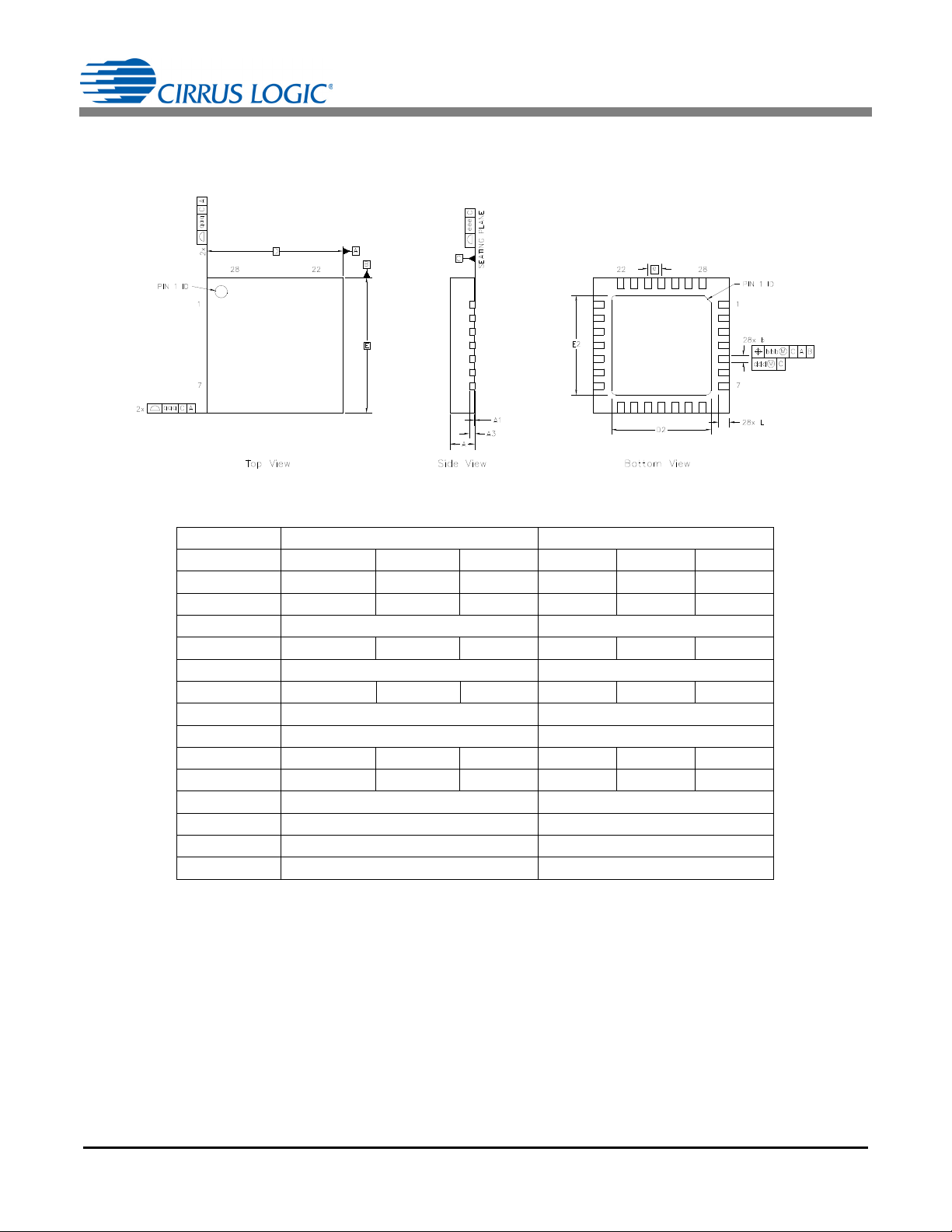
9. PACKAGE DIMENSIONS
28 QFN (5mmX5mm BODY with EXPOSED PAD) PACKAGE DRAWING
Notes:
1. Controlling dimensions are in millimeters.
2. Dimensions and tolerances per ASME Y14.5M.
3. This drawing conforms to JEDEC outline MO-220, variation VHHD-3.
4. Recommended reflow profile is per JEDEC / IPC J-STD-020.
CS5484
mm inch
Dimension MIN NOM MAX MIN NOM MAX
A 0.80 0.90 1.00 0.031 0.035 0.039
A1 0.00 0.02 0.05 0.000 0.001 0.002
A3 0.20 REF 0.008 REF
b 0.20 0.25 0.30 0.008 0.010 0.012
D 5.00 BSC 0.197 BSC
D2 3.50 3.65 3.80 0.138 0.144 0.150
e 0.50 BSC 0.020 BSC
E 5.00 BSC 0.197 BSC
E2 3.50 3.65 3.80 0.138 0.144 0.150
L 0.35 0.40 0.45 0.014 0.016 0.018
aaa 0.15 0.006
bbb 0.10 0.004
ddd 0.05 0.002
eee 0.08 0.003
66 DS981F3
Page 67
CS5484
Contacting Cirrus Logic Support
For all product questions and inquiries contact a Cirrus Logic Sales Representative.
To find the one nearest to you go to www.cirrus.com
IMPORTANT NOTICE
Cirrus Logic, Inc. and its subsidiaries (“Cirrus”) believe that the information contained in this document is accurate and reliable. However, the information is subject
to change without notice and is provided “AS IS” without warranty of any kind (express or implied). Customers are advised to obtain the latest version of relevant
information to verify, before placing orders, that information being relied on is current and complete. All products are sold subject to the terms and conditions of sale
supplied at the time of order acknowledgment, including those pertaining to warranty, indemnification, and limitation of liability. No responsibility is assumed by Cirrus
for the use of this information, including use of this information as the basis for manufacture or sale of any items, or for infringement of patents or other rights of third
parties. This document is the property of Cirrus and by furnishing this information, Cirrus grants no license, express or implied under any patents, mask work rights,
copyrights, trademarks, trade secrets or other intellectual property rights. Cirrus owns the copyrights associated with the information contained herein and gives consent for copies to be made of the information only for use within your organization with respect to Cirrus integrated circuits or other products of Cirrus. This consent
does not extend to other copying such as copying for general distribution, advertising or promotional purposes, or for creating any work for resale.
CERTAIN APPLICATIONS USING SEMICONDUCTOR PRODUCTS MAY INVOLVE POTENTIAL RISKS OF DEATH, PERSONAL INJURY, OR SEVERE PROPERTY OR ENVIRONMENTAL DAMAGE (“CRITICAL APPLICATIONS”). CIRRUS PRODUCTS ARE NOT DESIGNED, AUTHORIZED OR WARRANTED FOR USE
IN PRODUCTS SURGICALLY IMPLANTED INTO THE BODY, AUTOMOTIVE SAFETY OR SECURITY DEVICES, LIFE SUPPORT PRODUCTS OR OTHER CRITICAL APPLICATIONS. INCLUSION OF CIRRUS PRODUCTS IN SUCH APPLICATIONS IS UNDERSTOOD TO BE FULLY AT THE CUSTOMER'S RISK AND CIRRUS DISCLAIMS AND MAKES NO WARRANTY, EXPRESS, STATUTORY OR IMPLIED, INCLUDING THE IMPLIED WARRANTIES OF MERCHANTABILITY AND
FITNESS FOR PARTICULAR PURPOSE, WITH REGARD TO ANY CIRRUS PRODUCT THAT IS USED IN SUCH A MANNER. IF THE CUSTOMER OR CUSTOMER'S CUSTOMER USES OR PERMITS THE USE OF CIRRUS PRODUCTS IN CRITICAL APPLICATIONS, CUSTOMER AGREES, BY SUCH USE, TO FULLY
INDEMNIFY CIRRUS, ITS OFFICERS, DIRECTORS, EMPLOYEES, DISTRIBUTORS AND OTHER AGENTS FROM ANY AND ALL LIABILITY, INCLUDING ATTORNEYS' FEES AND COSTS, THAT MAY RESULT FROM OR ARISE IN CONNECTION WITH THESE USES.
Cirrus Logic, Cirrus, the Cirrus Logic logo designs, EXL Core, and the EXL Core logo design are trademarks of Cirrus Logic, Inc. All other brand and product names
in this document may be trademarks or service marks of their respective owners.
SPI is a trademark of Motorola, Inc.
10. ORDERING INFORMATION
Ordering Number Container Temperature Package
CS5484-INZ Bulk
CS5484-INZR Tape & Reel
11. ENVIRONMENTAL, MANUFACTURING, AND HANDLING INFORMATION
Part Number Peak Reflow Temp MSL Rating* Max Floor Life
CS5484-INZ
260°C 3 7 Days
* MSL (Moisture Sensitivity Level) as specified by IPC/JEDEC J-STD-020.
12. REVISION HISTORY
Revision Date Changes
PP1 APR 2012
F1 APR 2012
F2 JUN 2012 Updated ordering information.
F3 MAR 2013 Clarified context.
Preliminary release.
Edited for content and clarity.
-40 to +85 °C 28-pin QFN, Lead (Pb) Free
DS981F3 67
 Loading...