

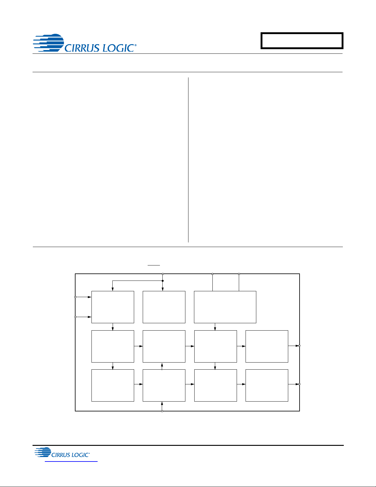
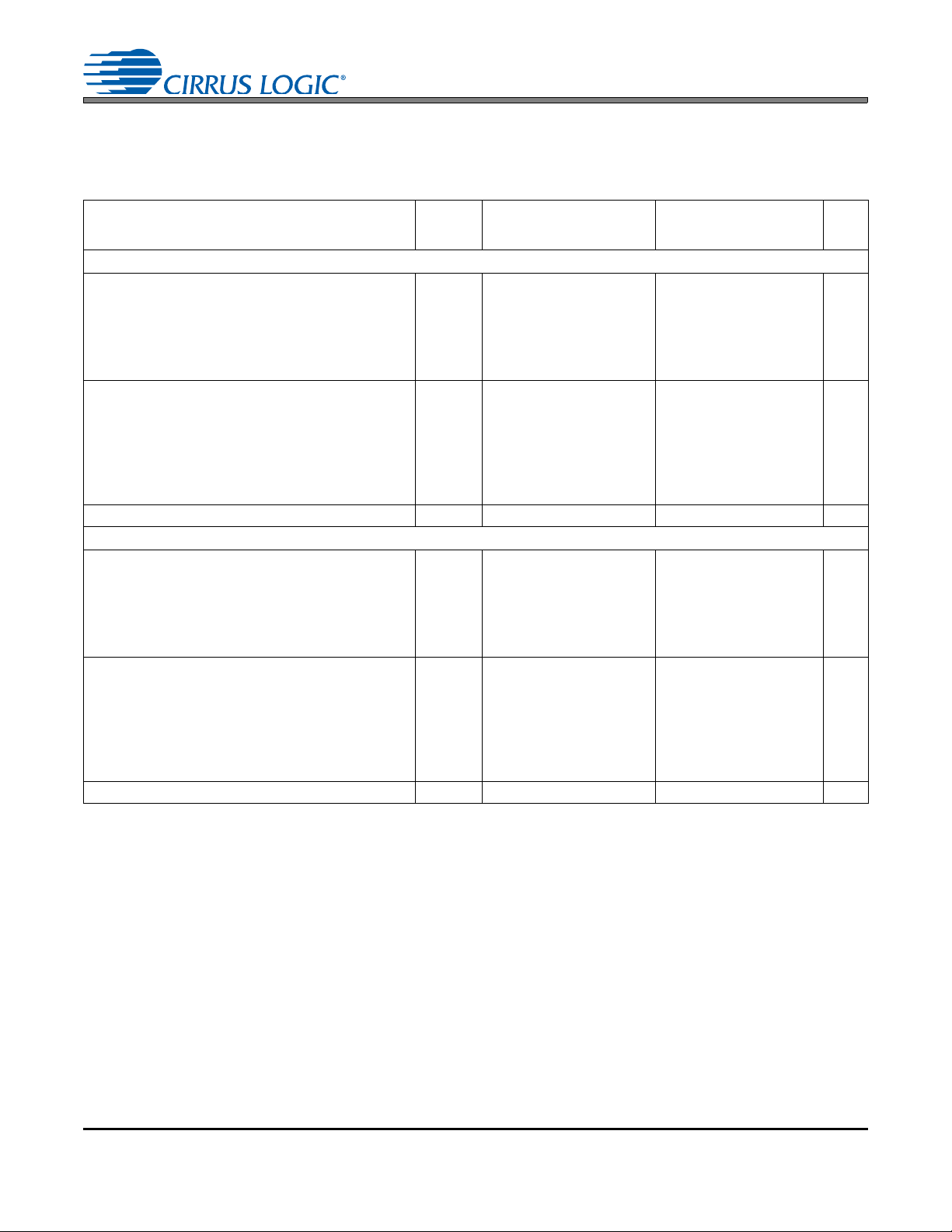
LRCK
3
SDATA
1
DEM/SCLK
2
MCLK
4
VA
AOUTL
8
AOUTR
5
Serial Input
Interface
Interpolator
Interpolator
De-emphasis
Modulator
Modulator
DAC
DAC
Voltage Reference
Analog
Low-Pass
Filter
Analog
Low-Pass
Filter
7
AGND
6
Confidential Draft
1/18/12
CS4334/5/8/9
8-Pin, 24-Bit, 96 kHz Stereo D/A Converter
Features
Complete Stereo DAC System: Interpolation,
D/A, Output Analog Filtering
24-Bit Conversion
96 dB Dynamic Range
-88 dB THD+N
Low Clock-Jitter Sensitivity
Single +5 V Power Supply
Filtered Line-Level Outputs
On-Chip Digital De-emphasis
Popguard
Functionally Compatible with CS4330/31/33
®
Technology
Description
The CS4334 family members are complete, stereo digital-to-analog output systems including interpolation,
1-bit D/A conversion and output analog filtering in an
8-pin package. The CS4334/5/8/9 support all major audio data interface formats, and the individual devices
differ only in the supported interface format.
The CS4334 family is based on Delta-Sigma modulation, where the modulator output controls the reference
voltage input to an ultra-linear analog low-pass filter.
This architecture allows for infinite adjustment of sample rate between 2 kHz and 100 kHz simply by
changing the master clock frequency.
The CS4334 family contains on-chip digital de-emphasis, operates from a single +5V power supply, and
requires minimal support circuitry. These features are
ideal for set-top boxes, DVD players, SVCD players,
and A/V receivers.
ORDERING INFORMATION
See “Ordering Information” on page 24
http://www.cirrus.com
Copyright Cirrus Logic, Inc. 2012
(All Rights Reserved)
JANUARY '12
DS248F6

TABLE OF CONTENTS
1. TYPICAL CONNECTION DIAGRAM ........... .... ... ... ... .......................................... .... ... ... ... ... .... .............. 4
2. CHARACTERISTICS AND SPECIFICATIONS ..................................................................................... 5
SPECIFIED OPERATING CONDITIONS.............................................................................................. 5
ABSOLUTE MAXIMUM RATINGS........................................................................................................5
ANALOG CHARACTERISTICS............................................................................................................. 6
POWER AND THERMAL CHARACTERISTICS ................................................................................... 8
DIGITAL INPUT CHARACTERISTICS.......................................................................... ... ... .... ... ... ... .... . 9
SWITCHING CHARACTERISTICS............................................... ... ... ... .... ......................................... 10
3. GENERAL DESCRIPTION ................................................................................................................. 12
3.1 Digital Interpolation Filter .............................................................................................................. 12
3.2 Delta-Sigma Modulator ................................................................................................................. 12
3.3 Switched-Capacitor DAC .............................................................................................................. 12
3.4 Analog Low-Pass Filter ................................................................................................................. 12
4. SYSTEM DESIGN ............................................................................................................................... 13
4.1 Master Clock ................................................................................................................................. 13
4.2 Serial Clock .................................................................................................................................. 13
4.2.1 External Serial Clock Mode ................................................................................................. 13
4.2.2 Internal Serial Clock Mode .. ... ... ... .... ................................................................................... 13
4.3 De-Emphasis ................................................................................................................................ 14
4.4 Initialization and Power-Down ...................................................................................................... 14
4.5 Output Transient Control .............................................................................................................. 14
4.6 Grounding and Power Supply Decoupling .................................................................................... 15
4.7 Analog Output and Filtering .......................................................................................................... 15
4.8 Overall Base-Rate Frequency Response ..................................................................................... 18
4.9 Overall High-Rate Frequency Response ......................................................................................19
4.10 Base Rate Mode Performance Plots .................................... ... ... .......................................... ... ...20
4.11 High Rate Mode Performance Plots ........................................................................... .... ... ... ... ... 21
5. PARAMETER DEFINITIONS ............................................................................................................... 22
6. REFERENCES ..................................................................................................................................... 22
7. PACKAGE DIMENSIONS ................................................................................................................... 23
8. ORDERING INFORMATION .................. ... ... .... ... ... ... .... ... ... ... .......................................... ... .... ............ 24
9. FUNCTIONAL COMPATIBILITY ...................... ... ... ... .... .......................................... ... ... ... ... .... ... ......... 24
10. REVISION HISTORY ......................................................................................................................... 25
CS4334/5/8/9
LIST OF FIGURES
Figure 1. Recommended Connection Diagram.........................................................................................4
Figure 2. Output Test Load..................................................... ... .... ......................................... .................. 8
Figure 3. Maximum Loading....................... ... ... .... ... ... ... .... ... ... ... .... ... ... ... .................................................. 9
Figure 4. Power vs. Sample Rate ............................................................................................................. 9
Figure 5. External Serial Mode Input Timing........................................................................................... 11
Figure 6. Internal Serial Mode Input Timing............................................................................................ 11
Figure 7. Internal Serial Clock Generation............................................................................................. 11
Figure 8. System Block Diagram................... ... .... ... ... ... .... ... ... ... .... ......................................... .... ............ 12
Figure 9. De-Emphasis Curve (Fs = 44.1kHz)........................................................................................ 14
Figure 10. CS4334 Data Format (I²S)............. ... .... ... ... ... .... ... ... ... .......................................... ... .... ............ 15
Figure 11. CS4335 Data Format............ ... ... ... ... .... ... .......................................... ... ... .... ... ... ... ... ................ 15
Figure 12. CS4338 Data Format............ ... ... ... ... .... ... .......................................... ... ... .... ... ... ... ... ................ 16
Figure 13. CS4339 Data Format............ ... ... ... ... .... ... .......................................... ... ... .... ... ... ... ... ................ 16
Figure 14. CS4334/5/8/9 Initialization and Power-Down Sequence ...................................... ... .... ... ... ... ... 17
Figure 15. Stopband Rejection..................................................................... .... ... ... ... .... ... ......................... 18
Figure 16. Transition Band.............................................. .... ... ... ... .... ... ... ... ... .... ... ... ................................... 18
Figure 17. Transition Band.............................................. .... ... ... ... .... ... ... ... ... .... ... ... ................................... 18
2
Figure 18. Passband Ripple............................................ .... ... .......................................... ... ... ................... 18
SERIAL DATA INPUT SDATA AOUTL ANALOG LEFT CHANNEL OUTPUT
DE-EMPHASIS / SCLK DEM/SCLK VA ANALOG POWER
LEFT / RIGHT CLOCK LRCK AGND ANALOG GROUND
MASTER CLOCK MCLK AOUTR ANALOG RIGHT CHANNEL OUTPUT
72
63
54
81
Figure 19. Stopband Rejection..................................................................... .... ... ... ... .... ... ......................... 19
Figure 20. Transition Band.............................................. .... ... ... ... .... ... ... ... ... .... ... ... ................................... 19
Figure 21. Transition Band.............................................. .... ... ... ... .... ... ... ... ... .... ... ... ................................... 19
Figure 22. Passband Ripple............................................ .... ... .......................................... ... ... ................... 19
Figure 23. 0 dBFS FFT (BRM) .................................................................................................................. 20
Figure 24. -60 dBFS FFT (BRM)........... ... ... ... ... ....................................................................................... 20
Figure 25. Idle Channel Noise FFT (BRM)....................................... ... ... ... ... .... ... ... ... .... ... ... ... ... .... ... ......... 20
Figure 26. Twin Tone IMD FFT (BRM)...................................................................................................... 20
Figure 27. THD+N vs. Amplitude (BRM)...................... ... .... ... ... ... .... ... ... ... ... ............................................. 20
Figure 28. THD+N vs. Frequency (BRM).................. ... ... .... ... .......................................... ... ... ... .... ... ... ...... 20
Figure 29. 0 dBFS FFT (HRM).................................................................................................................. 21
Figure 30. -60 dBFS FFT (HRM) . ... ....... ... ... ... ... ....................................................................................... 21
Figure 31. Idle Channel Noise FFT (HRM) ......................................... ... ... ... .... ... ... ... .... ... ... ... ... .... ... ......... 21
Figure 32. Twin Tone IMD FFT (HRM) ..................................................................................................... 21
Figure 33. THD+N vs. Amplitude (HRM)...... ... ... .... ... ... ... .... .......................................... ... ... ... ... .... ... ......... 21
Figure 34. THD+N vs. Frequency (HRM)........ ... .... ... ... ... .... ... ... ... .... ......................................... .... ... ......... 21
LIST OF TABLES
Table 1. Common Clock Frequencies ............................ .......................................... ................................ 13
PIN DESCRIPTIONS
CS4334/5/8/9
No. Pin Name I/O Pin Function and Description
Serial Audio Data Input - Two’s complement MSB-first serial data is input on this pin. The data is
1SDATAI
2DEM/SCLKI
3 LRCK I
4MCLKI
5AOUTROAnalog Right Channel Output - Typically 3.5 Vp-p for a full-scale input signal.
6AGNDIAnalog Ground - Analog ground reference is 0V.
7VAIAnalog Power - Analog power supply is nominally +5 V.
8AOUTLOAnalog Left Channel Output - Typically 3.5 Vp-p for a full-scale input signal.
clocked into the CS4334/5/8/9 via internal or external SCLK, and the channel is determined by
LRCK.
De-Emphasis/External Serial Clock Input - Used for de-emphasis filter control or external serial
clock input.
Left/Right Clock - Determines which channel is currently being input on the Audio Serial Data
Input pin, SDATA.
Master Clock - Frequency must be 256x, 384x, or 512x the input sample rate in BRM and either
128x or 192x the input sample rate in HRM.
3
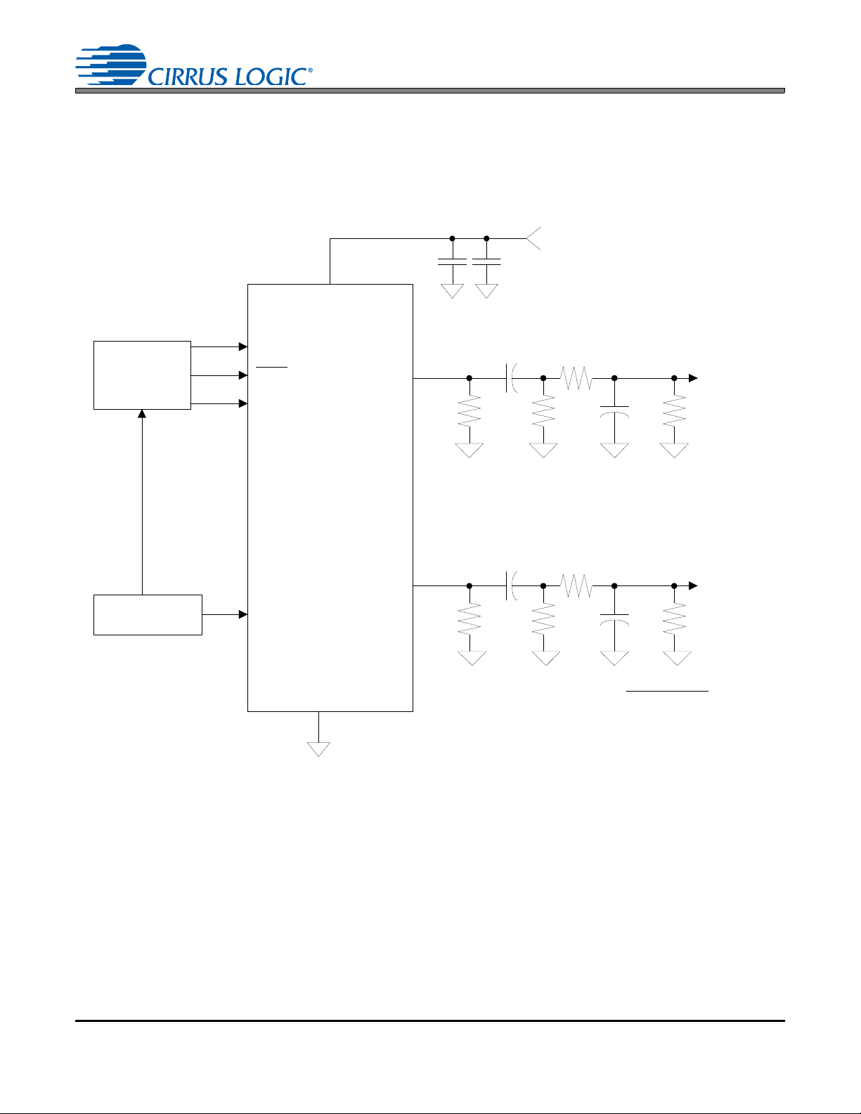
1. TYPICAL CONNECTION DIAGRAM
DEM/SCLK
6
Audio
Data
Processor
External C lock
MCLK
AGND
AOUTR
CS4334
CS4335
CS4338
CS4339
SDATA
LRCK
VA
AOUTL
3
1
2
4
7
0.1 µF
+
1µF
8
Left Audio
Output
5
Right Audio
Output
+5V
3.3 µF
10 k
C
560
+
R+560
C=
4
Fs(R 560)
R
L
3.3 µF
10 k
C
560
+
267 k
R
L
L
L
267 k
Figure 1. Recommended Connection Diagram
CS4334/5/8/9
4
CS4334/5/8/9
2. CHARACTERISTICS AND SPECIFICATIONS
(All Min/Max characteristics and specifications are guaranteed over the Specified Operating Conditions. Typical
performance characteristics and spe cif icat ion s ar e de riv e d from measurements taken at nominal supply voltages
and T
= 25C.)
A
SPECIFIED OPERATING CONDITIONS
(AGND = 0V; all voltages with respect to ground.)
Parameters Symbol Min Nom Max Units
DC Power Supply VA 4.75 5.0 5.5 V
Ambient Operating Temperature (Power Applied) -KSZ, -KSZR
-DSZ, -DSZR
T
A
-10
-40
-
-
+70
+85
C
C
ABSOLUTE MAXIMUM RATINGS
(AGND = 0V; all voltages with respect to ground.)
Parameters Symbol Min Max Units
DC Power Supply VA -0.3 6.0 V
Input Current, Any Pin Except Supplies I
Digital Input Voltage V
Ambient Operating Temperature (power applied) T
Storage Temperature T
in
IND
A
stg
WARNING:Operation at or beyond these limits may result in permanent damage to the device. Normal operation
is not guaranteed at these extremes.
-±10mA
-0.3 VA+0.4 V
-55 125 °C
-65 150 °C
5
CS4334/5/8/9
ANALOG CHARACTERISTICS
(Full-Scale Output Sine Wave, 997 Hz; Test load RL = 10 k, CL = 10 pF (see Figure 2). Fs for Base-Rate Mode =
48 kHz, Measurement Bandwidth 10 Hz to 20 kHz, unless otherwise specified; Fs for High-Rate Mode = 96 kHz,
Measurement Bandwidth 10 Hz to 40 kHz, unless otherwise specified.)
Base-Rate Mode High-Rate Mode
Parameter
Dynamic Performance for CS4334/5/8/9-KSZ, -KZSR
Dynamic Range (Note 1)
18 to 24-Bit
unweighted
A-Weighted
16-Bit unweighted
A-Weighted
Total Harmonic Distortion + Noise (Note 1)
18 to 24-Bit 0 dB
-20 dB
-60 dB
16-Bit 0 dB
-20 dB
-60 dB
Interchannel Isolation (1 kHz) - 94 - - 95 - dB
Dynamic Performance for CS4334/5/8/9-DSZ, -DSZR
Dynamic Range (Note 1)
18 to 24-Bit
unweighted
A-Weighted
16-Bit unweighted
A-Weighted
Total Harmonic Distortion + Noise (Note 1)
18 to 24-Bit 0 dB
-20 dB
-60 dB
16-Bit 0 dB
-20 dB
-60 dB
Interchannel Isolation (1 kHz) - 94 - - 95 - dB
Symbol Min Typ Max Min Typ Max Unit
88
91
86
89
THD+N
-
-
-
-
-
-
85
88
83
86
THD+N
-
-
-
-
-
-
93
96
91
94
-88
-73
-33
-86
-71
-31
93
96
91
94
-88
-73
-33
-86
-71
-31
-83
-68
-28
-81
-66
-26
-82
-65
-25
-70
-63
-23
-
-
-
-
-
-
-
-
91
89
88
86
-
-
-
-
-
-
-
-
-
-
-
-
-
-
-
-
90
96
88
94
-88
-70
-30
-86
-68
-28
90
96
88
94
-88
-70
-30
-86
-68
-28
-83
-65
-25
-81
-63
-23
-82
-62
-22
-80
-60
-20
-
dB
-
dB
-
dB
-
dB
dB
dB
dB
dB
dB
dB
-
dB
-
dB
-
dB
-
dB
dB
dB
dB
dB
dB
dB
Notes:
6
1. One LSB of triangular PDF dither added to data.
CS4334/5/8/9
ANALOG CHARACTERISTICS (Continued)
Base-Rate Mode High-Rate Mode
Parameter
Combined Digital and On-chip Anal o g Fi lt er R es p ons e
Passband (Note 3)
to -0.05 dB corner
to -0.1 dB corner
to -3 dB corner
Frequency Response 10 Hz to 20 kHz - .01 - +.08 -.05 - +.2 dB
Passband Ripple - - ±.08 - - ±.2 dB
StopBand .5465 - - .5770 - - Fs
StopBand Attenuation (Note 4) 50 - - 55 - - dB
Group Delay tgd - 9/Fs - - 4/Fs - s
Passband Group Delay Deviation 0 - 40 kHz
0 - 20 kHz
De-emphasis Error Fs = 32 kHz
Fs = 44.1 kHz
Fs = 48 kHz
Parameters Symbol Min Typ Max Units
DC Accuracy
Interchannel Gain Mismatch - 0.1 0.4 dB
Gain Error -±5- %
Gain Drift - 100 - ppm/°C
Analog Output
Full Scale Output Voltage 3.25 3.5 3.75 Vpp
Quiescent Voltage V
Max AC-Load Resistance (Note 6) R
Max Load Capacitance (Note 6) C
Symbol Min Typ Max Min Typ Max Unit
(Note 2)
0
-
0
- ±0.36/Fs - --±1.39/Fs
-
-
-
-
-
-
-
-
-
Q
L
L
.4780
-
.4996
+1.5/+0
+.05/-.25
-.2/-.4
-2.2-VDC
-3-k
- 100 - pF
0
0
-
-
-
±0.23/Fs
(Note 5)
.4650
.4982
-
-
Fs
Fs
Fs
s
s
dB
dB
dB
Notes:
2. Filter response is not tested but is guaranteed by design.
3. Response is clock dependent and will scale with Fs. Note that the response plots (Figures 15-22) have
been normalized to Fs and can be de-normalized by multiplying the X-axis scale by Fs.
4. For Base-Rate Mode, the Measurement Bandwidth is 0.5465 Fs to 3 Fs.
For High-Rate Mode, the Measurement Bandwidth is 0.577 Fs to 1.4 Fs.
5. De-emphasis is not available in High-Rate Mode.
6. Refer to Figure 3.
7
CS4334/5/8/9
AOUTx
AGND
10 µF
V
out
R
L
C
L
Figure 2. Output Test Load
POWER AND THERMAL CHARACTERISTICS
Parameters Symbol Min Typ Max Units
Power Supplies
Power Supply Current normal operation
power-down state
Power Dissipation (Note 7)
normal operation
power-down
Package Thermal Resistance
Power Supply Rejection Ratio (1 kHz) PSRR - 79 - dB
Notes:
7. Refer to Figure 4. Max Power Dissipation is measured at VA=5.5V.
I
A
I
A
JA
-
-
-
-
-110-°C/Watt
15
40
75
0.2
19
104
-
mW
-
mW
mA
A
8

CS4334/5/8/9
100
50
75
25
2.5
51015
Safe Operating
Region
Capacitive Load -- C (pF)
L
Resistive Load -- R (k)
L
125
3
20
Figure 3. Maximum Loading Figure 4. Power vs. Sample Rate
75
50
30
Power (mW)
Sample Rate (kHz)
B
R
M
H
R
M
70
65
60
55
40 50 60 70 80 90
100
DIGITAL INPUT CHARACTERISTICS
Parameters Symbol Min Typ Max Units
High-Level Input Voltage V
Low-Level Input Voltage V
Input Leakage Current (Note 8) I
IH
IL
in
Input Capacitanc e - 8 - pF
Notes:
8. I
for CS433X LRCK is ±20A max.
in
2.0 - - V
--0.8V
--±10A
9

CS4334/5/8/9
1
128Fs
----------------------
1
64Fs
-------------------
1
SCLK
---------------- -
tsclkw
2
------------------
1
512Fs
----------------------10+
1
512Fs
----------------------15+
1
384Fs
----------------------15+
SWITCHING CHARACTERISTICS
Parameters Symbol Min Typ Max Units
Input Sample Rate Fs 2 - 100 kHz
MCLK Pulse Width High MCLK/LRCK = 512 10 - 1000 ns
MCLK Pulse Width Low MCLK/LRCK = 512 10 - 1000 ns
MCLK Pulse Width High MCLK / LRCK = 384 or 192 21 - 1000 ns
MCLK Pulse Width Low MCLK / LRCK = 384 or 192 21 - 1000 ns
MCLK Pulse Width High MCLK / LRCK = 256 or 128 31 - 1000 ns
MCLK Pulse Width Low MCLK / LRCK = 256 or 128 31 - 1000 ns
External SCLK Mode
LRCK Duty Cycle (External SCLK only) 40 50 60 %
SCLK Pulse Width Low t
SCLK Pulse Width High t
SCLK Period Base-Rate Mode
sclkl
sclkh
t
sclkw
MCLK / LRCK = 512, 256 or 384
SCLK Period High-Rate Mode
t
sclkw
MCLK / LRCK = 128 or 192
SCLK rising to LRCK edge delay t
SCLK rising to LRCK edge setup time t
SDATA valid to SCLK rising setup time t
SCLK rising to SDATA hold time t
slrd
slrs
sdlrs
sdh
Internal SCLK Mode
LRCK Duty Cycle (Internal SCLK only) (Note 9) -50-%
t
SCLK Period (Note 10)
sclkw
20 - - ns
20 - - ns
--ns
--ns
20 - - ns
20 - - ns
20 - - ns
20 - - ns
--ns
SCLK rising to LRCK edge
SDATA valid to SCLK rising setup time
SCLK rising to SDATA hold time
MCLK / LRCK = 512, 256 or 128
SCLK rising to SDATA hold time
MCLK / LRCK = 384 or 192
Notes:
9. In Internal SCLK Mode, the Duty Cycle must be 50% 1/2 MCLK Period.
10. The SCLK / LRCK ratio may be either 32, 48, or 64. This ratio depends on part type and MCLK/LRCK
ratio. (See figures Figures 10-13)
t
sclkr
t
sdlrs
t
sdh
t
sdh
--s
--ns
--ns
--ns
10

CS4334/5/8/9
sclkh
t
slrs
t
slrd
t
sdlrs
t
sdh
t
sclkl
t
SDATA
SCLK
LRCK
Figure 5. External Serial Mode Input Timing
SDATA
*INTERNAL SCLK
LRCK
sclkw
t
sdlrstsdh
t
sclkr
t
Figure 6. Internal Serial Mode Input Timing
The SCLK pulses shown are internal to the CS4334/5/8/9.
SDATA
LRCK
MCLK
*INTERNAL SCLK
1
N
2
N
Figure 7. Internal Serial Clock Generation
* The SCLK pulses shown are internal to the CS4334/5/8/9.
N equals MCLK divided by SCLK
11

CS4334/5/8/9
Interpolator
Delta-Sigma
Modulator
DAC
Analog
Low-Pass
Filter
Analog
Output
Digital
Input
Figure 8. System Block Diagram
3. GENERAL DESCRIPTION
The CS4334 family of devices offers a complete stereo digital-to-analog system including digital interpolation,
fourth-order delta-sigma digital-to-analog conversion, digital de-emphasis and analog filtering, as shown in
Figure 8. This architecture provides a high tolerance to clock jitter.
The primary purpose of using delta-sigma modulation techniques is to avoid the limitations of resistive laser trimmed
digital-to-analog converter architectures by using an inherently linear 1-bit digital-to-analog converter. The advantages of a 1-bit digital-to-analog converter include: idea l differential line arity, no distortion mech anisms due to resistor matching errors and no linearity drift over time and temperature due to variations in resistor values.
The CS4334 family of devices supports two modes of operation. The devices operate in Base Rate Mode (BRM)
when MCLK/LRCK is 256, 384 or 512 and in High Rate Mode (HRM) when MCLK/LRCK is 128 or 192. High Rate
Mode allows input sample rates up to 100 kHz.
3.1 Digital Interpolation Filter
The digital interpolation filter increases the sample rate, Fs, by a factor of 4 and is followed by a 32× digital
sample-and-hold (16× in HRM). This filter eliminates images of the baseband audio signal which exist at
multiples of the input sample rate. The resulting frequency spectrum has images of the inpu t sig nal at multiples of 4 Fs. These images are easily removed by the on-chip analog low-pass filter and a simple external
analog filter (see Figure 1).
3.2 Delta-Sigma Modulator
The interpolation filter is followed by a fourth order delta-sigma modulator which converts the interpolation
filter output into 1-bit data at a rate of 128 Fs in BRM (or 64 Fs in HRM).
3.3 Switched-Capacitor DAC
The delta-sigma modulator is followed by a digital-to-anal og converter which tran slates the 1-bit data into a
series of charge packets. The magnitude of the charge in each packet is determined by sampling of a voltage reference onto a switched capacitor, where the polarity of each packet is controlled by the 1-bit data.
This technique greatly reduces the sensitivity to clock jitter and provides low-pass filtering of the output.
3.4 Analog Low-Pass Filter
The final signal stage consists of a continuous-time low-pass filter which serves to smooth the output and
attenuate out-of-band noise.
12

CS4334/5/8/9
4. SYSTEM DESIGN
The CS4334 family accepts data at standard audio sample rates including 48, 44.1 and 32 kHz in BRM and 96, 88.2
and 64 kHz in HRM. Audio data is input via the serial data input pin (SDATA). The Left/Right Clock (LRCK) define s
the channel and delineation of data, and the Serial Clock (SCLK) clocks audio data into the input data buffer. The
CS4334/5/8/9 differ in serial data formats as shown in Figures 10-13.
4.1 Master Clock
MCLK must be either 256x, 384x or 512x the desired inp ut sample rate in BRM an d either 128x or 192x the
desired input sample rate in HRM. The LRCK frequency is equal to Fs, the frequency at which words for
each channel are input to the device. The MCLK-to-LRCK frequency ratio is detected automatically during
the initialization sequence by counting the number of MCLK tran sitions during a single LRCK period. Internal
dividers are set to generate the proper clocks. Table 1 illustrates several standard audio sample rates and
the required MCLK and LRCK frequencies. Please note there is no required phase relationship, but MCLK,
LRCK and SCLK must be synchronous.
MCLK (MHz)
LRCK
(kHz)
32 4.0960 6.1440 8.1920 12.2880 16.3840
44.1 5.6448 8.4672 11.2896 16.9344 22.5792
48 6.1440 9.2160 12.2880 18.4320 24.5760
64 8.1920 12.2880 - - -
88.2 11.2896 16.9344 - - 96 12.2880 18.4320 - - -
Table 1. Common Clock Frequencies
HRM BRM
128x 192x 256x 384x 512x
4.2 Serial Clock
The serial clock controls the shifting of data into the input data buffers. The CS4334 family supports both
external and internal serial clock generation modes. Refer to Figures 10-13 for data formats.
4.2.1 External Serial Clock Mode
The CS4334 family will enter the External Serial Clock Mode when 16 low to high transitions are detected
on the DEM/SCLK pin during any phase of the LRCK period. When this mode is e nabled, the Internal Serial Clock Mode and de-emphasis filter cannot be accessed. The CS4334 family will switch to Internal Serial Clock Mode if no low to high transitions are detected on the DEM/SCLK pin for 2 consecutive frames
of LRCK. Refer to Figure 14.
4.2.2 Internal Serial Clock Mode
In the Internal Serial Clock Mo de, the serial clock is intern ally derived an d synchronou s with MCLK and
LRCK. The SCLK/LRCK frequency ratio is either 32, 48, or 64 depending upon data format. Operation in
this mode is identical to operation with an external serial clock synchronized with LRCK. This mode allows
access to the digital de-emphasis function. Refer to Figures 10 - 14 for details.
13
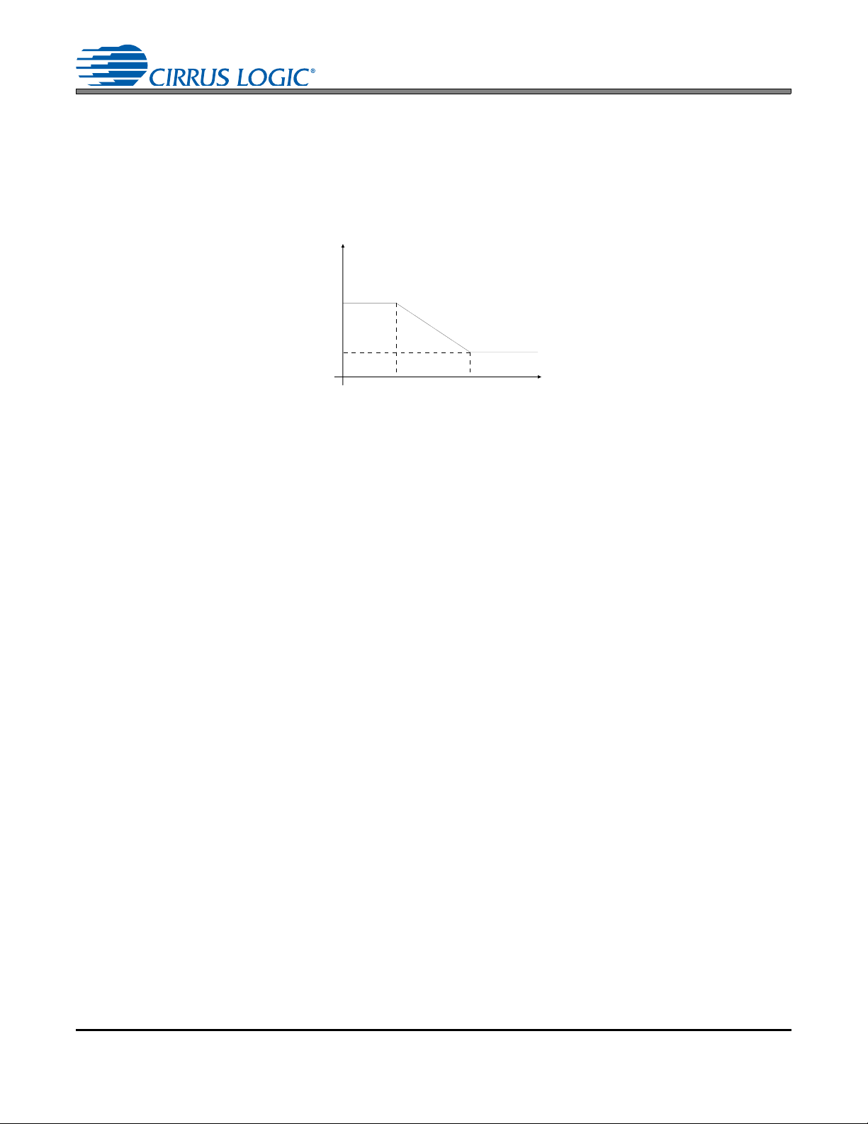
4.3 De-Emphasis
Gain
dB
-10dB
0dB
Frequency
T2 = 15 µs
T1=50 µs
F1 F2
3.183 kHz 10.61 kHz
Figure 9. De-Emphasis Curve (Fs = 44.1kHz)
The CS4334 family includes on-chip digital de-emphasis. Figure 9 shows the de-emphasis curve for Fs
equal to 44.1 kHz. The frequency response of the de-emphasis curve will scale proportionally with changes
in sample rate, Fs.
The de-emphasis filter is active (inactive) if the DEM/SCLK pin is low (high) for 5 consecutive falling edges
of LRCK. This function is available only in the internal serial clock mode.
4.4 Initialization and Power-Down
CS4334/5/8/9
The Initialization and Power-Down sequence flow chart is shown in Figure 14. The CS4334 family enters
the Power-Down State upon initial power-up. The interpolation filters and delta-sigma modulator s are reset,
and the internal voltage reference, one-bit digital-to-analog converters and switched-capacitor low-pass filters are powered down. The device will remain in the Power-Down mode until MCLK and LRCK are present.
Once MCLK and LRCK are detected, MCLK occurrences are counted over one LRCK period to determine
the MCLK /LRCK frequ ency ra tio. Po wer is then a pplied to the internal voltage reference. Finally, power is
applied to the D/A converters and switched-capacitor filters, and the analog outputs will ramp to the quiescent
voltage, V
.
Q
4.5 Output Transient Control
The CS4334 family uses Popguard® technology to minimize the effects of output transients during powerup and power-down. This technique eliminates the audio transients commonly produced by single-ended
single-supply converters when it is implemented with external DC-blocking capacitors connected in series
with the audio outputs. To make best use of this feature, it is necessary to understand its operation.
When the device is initially powered-up, the audio outputs, AOUTL and AOUTR, are clamped to AGND. After a short delay of approximately 1000 sa mple per iods, eac h output be gins to ram p towards it s quiesce nt
voltage, V
gradual voltage ramping allows time for the external DC-blocking capacitor to charge to V
blocking the quiescent DC voltage.
To prevent transients at power-down, the d evice must first enter its power-down state. This is accomplished
by removing MCLK or LRCK. When this occurs, audio outpu t ceases and the internal output buffers are disconnected from AOUTL and AOUTR. A soft-start current sink is substituted in place of AOUTL and AOUTR
which allows the DC-blocking capacitors to slowly discharge. Once this charge is dissipated, the power to
the device may be turned off, and the system is ready for the next power-on.
. Approximately 10,000 sample cycles later, the outputs reach VQ and audio output begins. This
Q
, effectively
Q
To prevent an audio transient at the next power-on, the DC-blocking capacitors must fully discharge before
turning off the power or exiting the power-down state. If full discharge does not occur, a transient will occur
when the audio outputs are initially clamped to AGND. The time that the device must remain in the power-
14

down state is related to the value of the DC-blocking capacitance. For example, with a 3.3 F capacitor, the
LRCK
SCLK
Left Channel
Right Channel
SDATA +3 +2 +1
LSB
+5 +4
MSB
-1 -2 -3 -4 -5
+3 +2 +1
LSB
+5 +4
MSB
-1 -2 -3 -4
Internal SCLK Mode External SCLK Mode
I²S, 16-Bit data and INT SCLK = 32 Fs if
MCLK/LRCK = 512, 256 or 128
I²S, Up to 24-Bit data and INT SCLK = 48 Fs if
MCLK/LRCK = 384 or 192
I²S, up to 24-Bit Data
Data Valid on Rising Edge of SCLK
Figure 10. CS4334 Data Format (I²S)
LRCK
SCLK
Left Channel
Right Channel
SDATA +3 +2 +1
LSB
+5 +4
MSB
-1 -2 -3 -4 -5
+3 +2 +1
LSB
+5 +4
MSB
-1 -2 -3 -4
Internal SCLK Mode External SCLK Mode
Left Justified, up to 24-Bit Data
INT SCLK = 64 Fs if MCLK/LRCK = 512, 256 or 128
INT SCLK = 48 Fs if MCLK/LRCK = 384 or 192
Left Justified, up to 24-Bit Data
Data Valid on Rising Edge of SCLK
Figure 11. CS4335 Data Format
time that the device must remain in the power-down state will be approximately 0.4 seconds.
4.6 Grounding and Power Supply Decoupling
As with any high resolution converter, the CS4334 family requires careful attention to power supply and
grounding arrangements to optimize performance. Figure 1 shows the recommended power arrangement
with VA connected to a clean +5V supply. For best performance, decoupling capacitors should be located
as close to the device package as possible with the smallest capacitor closest.
4.7 Analog Output and Filtering
The analog filter present in the CS4334 family is a switched-capacitor filter followed by a continuous time
low pass filter. Its response, combined with that of the digita l interpolator, is given in Figures 15 - 22.
CS4334/5/8/9
15

CS4334/5/8/9
LRCK
SCLK
Left Channel
Right Channel
SDATA
6543210987
15 14 13 12 11 10
6543210987
15 14 13 12 11 10
32 clocks
Internal SCLK Mode External SCLK Mode
Right Justified, 16-Bit Data
INT SCLK = 32 Fs if MCLK/LRCK = 512, 256 or 128
INT SCLK = 48 Fs if MCLK/LRCK = 384 or 192
Right Justified, 16-Bit Data
Data Valid on Rising Edge of SCLK
SCLK Must Have at Least 32 Cycles per LRCK Period
Figure 12. CS4338 Data Format
LRCK
SCLK
Left Channel
Right Channel
SDATA
6543210987
15 14 13 12 11 10
10
6543210987
15 14 13 12 11 10
17 16 17 16
32 clocks
Internal SCLK Mode External SCLK Mode
Right Justified, 18-Bit Data
INT SCLK = 64 Fs if MCLK/LRCK = 512, 256 or 128
INT SCLK = 48 Fs if MCLK/LRCK = 384 or 192
Right Justified, 18-Bit Data
Data Valid on Rising Edge of SCLK
SCLK Must Have at Least 36 Cycles per LRCK Period
Figure 13. CS4339 Data Format
16

CS4334/5/8/9
Figure 14. CS4334/5/8/9 Initialization and Power-Down Sequence
17

4.8 Overall Base-Rate Frequency Response
Figure 15. Stopband Rejection Figure 16. Transition Band
Figure 17. Transition Band Figure 18. Passband Ripple
CS4334/5/8/9
18

4.9 Overall High-Rate Frequency Response
Figure 19. Stopband Rejection Figure 20. Transition Band
Figure 21. Transition Band Figure 22. Passband Ripple
CS4334/5/8/9
19

4.10 Base Rate Mode Performance Plots
-140
+0
-130
-120
-110
-100
-90
-80
-70
-60
-50
-40
-30
-20
-10
d
B
r
A
2k 20k4k 6k 8k 10k 12k 14k 16k 18k
Hz
2k
4k 6k 8k 10k 12k 14k 16k 18k
-140
-130
-120
-110
-100
-90
-80
-70
-60
-50
-40
-30
-20
-10
+0
dBr A
Hz
20k
+0
-10
-20
-30
-40
-50
-60
-70
-80
-90
-100
-110
-120
-130
-140
dBr A
2k 6k4k 8k
10k
12k 14k 16k 18k
20k
Hz
-140
+0
-130
-120
-110
-100
-90
-80
-70
-60
-50
-40
-30
-20
-10
d
B
r
A
2k 20k4k 6k 8k 10k 12k 14k 16k 18k
Hz
20k
2k
4k 6k 8k 10k 12k 14k 16k 18k
-140
-130
-120
-110
-100
-90
-80
-70
-60
-50
-40
-30
-20
-10
+0
dBr A
Hz
20k
2k 6k4k 8k
10k
12k 14k 16k 18k 20k
Hz
+0
-10
-20
-30
-40
-50
-60
-70
-80
-90
-100
-110
-120
-130
-140
dBr A
(16k FFT of a 1 kHz input signal)
Figure 23. 0 dBFS FFT (BRM)
(16k FFT of a 1 kHz input signal)
Figure 24. -60 dBFS FFT (BRM)
-140
+0
-130
-120
-110
-100
-90
-80
-70
-60
-50
-40
-30
-20
-10
d
B
r
A
2k 20k4k 6k 8k 10k 12k 14k 16k 18k
Hz
2k
4k 6k 8k 10k 12k 14k 16k 18k
-140
-130
-120
-110
-100
-90
-80
-70
-60
-50
-40
-30
-20
-10
+0
dBr A
Hz
20k
+0
-10
-20
-30
-40
-50
-60
-70
-80
-90
-100
-110
-120
-130
-140
dBr A
2k 6k4k 8k 10k 12k 14k 16k 18k
20k
Hz
-140
+0
-130
-120
-110
-100
-90
-80
-70
-60
-50
-40
-30
-20
-10
d
B
r
A
2k 20k4k 6k 8k 10k 12k 14k 16k 18k
Hz
2k
4k 6k 8k 10k 12k 14k 16k 18k
-140
-130
-120
-110
-100
-90
-80
-70
-60
-50
-40
-30
-20
-10
+0
dBr A
Hz
20k
+0
-10
-20
-30
-40
-50
-60
-70
-80
-90
-100
-110
-120
-130
-140
dBr A
2k 6k4k 8k
10k
12k 14k 16k 18k
20k
Hz
(16k FFT with no input signal)
Figure 25. Idle Channel Noise FFT (BRM)
(16k FFT of intermodulation distortion using 13 kHz and 14 kHz i nput signals)
Figure 26. Twin Tone IMD FFT (BRM)
-110
-60
-100
-90
-80
-70
d
B
r
A
-60 +0-50 -40 -30 -20 -10
dBFS
-50 -40 -30 -20 -10
dBFS
-60 +0
-110
-100
-90
-80
-70
-60
dBr A
-110
+0
-100
-90
-80
-70
-60
-50
-40
-30
-20
-10
d
B
r
A
20 20k50 100 200 500 1k 2k 5k 10k
Hz
-110
-100
-90
-80
-70
-60
-50
-40
-30
-20
-10
+0
d
B
r
A
20 50 100
200
500 1k 2k 5k 10k 20k
Hz
+0
-10
-20
-30
-40
-50
-60
-70
-80
-90
-100
-110
dBr A
100
50 200 500 1k 2k
5k 10k
Hz
20 20k
(THD+N plots measured using a 1kHz 24-bit dithered input signal)
Figure 27. THD+N vs. Amplitude (BRM)
(THD+N plots measured using a 1kHz 24-bit dithered input signal)
Figure 28. THD+N vs. Frequency (BRM)
All measurements were taken from the CDB4334 evaluation board using the Audio Precision Dual Domain
System Two Cascade.
CS4334/5/8/9
20

4.11 High Rate Mode Performance Plots
-140
+0
-130
-120
-110
-100
-90
-80
-70
-60
-50
-40
-30
-20
-10
d
B
r
A
2k 20k4k 6k 8k 10k 12k 14k 16k 18k
Hz
2k
4k 6k 8k 10k 12k 14k 16k 18k
-140
-130
-120
-110
-100
-90
-80
-70
-60
-50
-40
-30
-20
-10
+0
dBr A
Hz
20k
+0
-10
-20
-30
-40
-50
-60
-70
-80
-90
-100
-110
-120
-130
-140
dBr A
2k 6k4k 8k
10k
12k 14k 16k 18k
20k
Hz
-140
+0
-130
-120
-110
-100
-90
-80
-70
-60
-50
-40
-30
-20
-10
d
B
r
A
2k 20k4k 6k 8k 10k 12k 14k 16k 18k
Hz
2k
4k 6k 8k 10k 12k 14k 16k 18k
-140
-130
-120
-110
-100
-90
-80
-70
-60
-50
-40
-30
-20
-10
+0
dBr A
Hz
20k
+0
-10
-20
-30
-40
-50
-60
-70
-80
-90
-100
-110
-120
-130
-140
dBr A
2k 6k4k 8k
10k
12k 14k 16k 18k
20k
Hz
(16k FFT of a 1 kHz input signal)
Figure 29. 0 dBFS FFT (HRM)
(16k FFT of a 1 kHz input signal)
Figure 30. -60 dBFS FFT (HRM)
-140
+0
-130
-120
-110
-100
-90
-80
-70
-60
-50
-40
-30
-20
-10
d
B
r
A
2k 20k4k 6k 8k 10k 12k 14k 16k 18k
Hz
2k
4k 6k 8k 10k 12k 14k 16k 18k
-140
-130
-120
-110
-100
-90
-80
-70
-60
-50
-40
-30
-20
-10
+0
dBr A
Hz
20k
+0
-10
-20
-30
-40
-50
-60
-70
-80
-90
-100
-110
-120
-130
-140
dBr A
2k 6k4k 8k 10k 12k 14k 16k 18k
20k
Hz
Audio Precision 08/05/99 11:11:36D-A CCIF IMD vs AMPLITUDE
-140
+0
-130
-120
-110
-100
-90
-80
-70
-60
-50
-40
-30
-20
-10
d
B
r
A
2k 20k4k 6k 8k 10k 12k 14k 16k 18k
Hz
2k
4k 6k 8k 10k 12k 14k 16k 18k
-140
-130
-120
-110
-100
-90
-80
-70
-60
-50
-40
-30
-20
-10
+0
dBr A
Hz
20k
+0
-10
-20
-30
-40
-50
-60
-70
-80
-90
-100
-110
-120
-130
-140
dBr A
2k 6k4k 8k
10k
12k 14k 16k 18k
20k
Hz
(16k FFT with no input signal)
Figure 31. Idle Channel Noise FFT (HRM)
(16k FFT of intermodulation distortion using 13 kHz and 14 kHz i nput signals)
Figure 32. Twin Tone IMD FFT (HRM)
-110
-60
-100
-90
-80
-70
d
B
r
A
-60 +0-50 -40 -30 -20 -10
dBFS
-50 -40 -30 -20 -10
dBFS
-60 +0
-110
-100
-90
-80
-70
-60
dBr A
-110
+0
-100
-90
-80
-70
-60
-50
-40
-30
-20
-10
d
B
r
A
20 20k50 100 200 500 1k 2k 5k 10k
Hz
-110
-100
-90
-80
-70
-60
-50
-40
-30
-20
-10
+0
d
B
r
A
20 50 100
200
500 1k 2k 5k 10k 20k
Hz
100
50 200 500 1k 2k
5k 10k
Hz
20 20k
+0
-10
-20
-30
-40
-50
-60
-70
-80
-90
-100
-110
dBr A
(THD+N plots measured using a 1kHz 24-bit dithered input signal)
Figure 33. THD+N vs. Amplitude (HRM)
(THD+N plots measured using a 1kHz 24-bit dithered input signal)
Figure 34. THD+N vs. Frequency (HRM)
All measurements were taken from the CDB4334 evaluation board using th e Audi o Precision Du al Domain
System Two Cascade.
CS4334/5/8/9
21

5. PARAMETER DEFINITIONS
Total Harmonic Distortion + Noise (THD+N)
The ratio of the rms value of the signal t o the rms su m of all other spectral components over the specified
bandwidth (typically 10Hz to 20kHz), including distortion components. Expressed in decibels.
Dynamic Range
The ratio of the full scale rms value of the signal to the rms sum of all other spectral components over the
specified bandwidth. Dynamic range is a signal-to-noise measurement over the specified bandwidth made
with a -60 dBFS signal. 60 dB is then added to the resulting measurement to refer the measurement to full
scale. This technique ensures that the distortion components are be low the noise level and do not effect the
measurement. This measurement technique has been accepted by the Audio Engineering Society, AES171991, and the Electronic Industries Association of Japan, EIAJ CP-307.
Interchannel Isolation
A measure of crosstalk between the left and right channels. Measured for each channel at the converter's
output with all zeros to the input under test and a full-scale signa l applied to the other channel. Units in d ecibels.
Interchannel Gain Mismatch
The gain difference between left and right channels. Units in decibels.
CS4334/5/8/9
Gain Error
The deviation from the nominal full-scale analog output for a full-scale digital input.
Gain Drift
The change in gain value with temperature. Units in ppm/°C.
6. REFERENCES
1. "How to Achieve Optimum Performance from Delta-Si gma A/D & D/A Conver te rs" by Steven Har ris. Paper
presented at the 93rd Convention of the Audio Engineering Society, October 1992.
2. CDB4334/5/8/9 Evaluation Board Datasheet
22

7. PACKAGE DIMENSIONS
8L SOIC (150 MIL BODY) PACKAGE DRAWING
D
H
E
e
b
A1
A
c
L
SEATING
PLANE
1
CS4334/5/8/9
INCHES MILLIMETERS
DIM MIN MAX MIN MAX
A 0.053 0.069 1.35 1.75
A1 0.004 0.010 0.10 0.25
b 0.013 0.020 0.33 0.51
c 0.007 0.010 0.19 0.25
D 0.189 0.197 4.80 5.00
E 0.150 0.157 3.80 4.00
e 0.040 0.060 1.02 1.52
H 0.228 0.244 5.80 6.20
L 0.016 0.050 0.40 1.27
0° 8° 0° 8°
JEDEC # : MS-012
23

8. ORDERING INFORMATION
Model Temperature Package Container Serial Interface
CS4334-KSZ -10 to +70 °C 8-pin Plastic SOIC, lead free Rail 16 to 24-bit, I²S
CS4335-KSZ -10 to +70 °C 8-pin Plastic SOIC, lead free Rail 16 to 24-bit, left justified
CS4338-KSZ -10 to +70 °C 8-pin Plastic SOIC, lead free Rail 16-bit, right justified
CS4339-KSZ -10 to +70 °C 8-pin Plastic SOIC, lead free Rail 18-bit, right justified, 32 F
CS4334-KSZR -10 to +70 °C 8-pin Plastic SOIC, lead free Tape & reel 16 to 24-bit, I²S
CS4335-KSZR -10 to +70 °C 8-pin Plastic SOIC, lead free Tape & reel 16 to 24-bit, left justified
CS4338-KSZR -10 to +70 °C 8-pin Plastic SOIC, lead free Tape & reel 16-bit, right justified
CS4339-KSZR -10 to +70 °C 8-pin Plastic SOIC, lead free Tape & reel 18-bit, right justified, 32 F
CS4334-DSZ -40 to +85 °C 8-pin Plastic SOIC, lead free Rail 16 to 24-bit, I²S
CS4335-DSZ -40 to +85 °C 8-pin Plastic SOIC, lead free Rail 16 to 24-bit, left justified
CS4338-DSZ -40 to +85 °C 8-pin Plastic SOIC, lead fre e Rail 16-bit, right justified
CS4339-DSZ -40 to +85 °C 8-pin Plastic SOIC, lead free Rail 18-bit, right justified, 32 F
CS4334-DSZR -40 to +85 °C 8-pin Plastic SOIC, lead free Tape & reel 16 to 24-bit, I²S
CS4335-DSZR -40 to +85 °C 8-pin Plastic SOIC, lead free Tape & reel 16 to 24-bit, left justified
CS4338-DSZR -40 to +85 °C 8-pin Plastic SOIC, lead free Tape & reel 16-bit, right justified
CS4339-DSZR -40 to +85 °C 8-pin Plastic SOIC, lead free Tape & reel 18-bit, right justified, 32 F
9. FUNCTIONAL COMPATIBILITY
CS4330-KS CS4339-KSZx
CS4331-KS CS4334-KSZx
CS4333-KS CS4338-KSZx
CS4330-BS CS4339-DSZx
CS4331-BS CS4334-DSZx
CS4333-BS CS4338-DSZx
CS4334/5/8/9
Internal SCLK mode
s
Internal SCLK mode
s
Internal SCLK mode
s
Internal SCLK mode
s
24

10.REVISION HISTORY
Contacting Cirrus Logic Support
For all product questions and inquiries, contact a Cirrus Logic Sales Representative.
To find the one nearest you, go to www.cirrus.com.
IMPORTANT NOTICE
Cirrus Logic, Inc. and its subsidiaries ("Cirrus") believe that the information contained in this document is accurate and reliable. However, the information is subject
to change without not ice and is pr ovided "AS IS" witho ut warr anty of any kind (express or implied). Customers are advised to obtain the latest version of relevant
information to verify, before placing orders, that information being relied on is current and complete. All products are sold subject to the terms and conditions of sale
supplied at the time of order acknowledgment, including those pertaining to warranty, indemnification, and limitation of liability. No responsibility is assumed by Cirrus
for the use of this information, including use of this information as the basis for manufacture or sale of any items, or for infringement of patents or other rights of third
parties. This document is the property of Cirrus and by furnishing this information, Cirrus grants no license, express or implied under any patents, mask work rights,
copyrights, trademarks, trade secrets or other inte llectual property rig hts. Cirrus owns the copyrights associated with the information contained herein and gives consent for copies to be made of the information only for use within your organization with respect to Cirrus integrated circuits or other products of Cirrus. This consent
does not extend to other copying such as copying for general distribution, advertising or promotional purposes, or for creating any work for resale.
CERTAIN APPLICATIONS USING SEMICONDUCTOR PRODUCTS MAY INVOLVE POTENTIAL RISKS OF DEATH, PERSONAL I N JURY, OR SEVERE PROPERTY OR ENVIRONMENTAL DAMAGE (“CRITICAL APPLICATIONS”). CIRRUS PRODUCTS ARE NOT DESIGNED, AUTHORIZED OR WARRANTED FOR USE
IN PRODUCTS SURGICALLY IMPLANTED INTO THE BODY, AUTOMOTIVE SAFETY OR SECURITY DEVICES, LIFE SUPPORT PRODUCTS OR OTHER CRITICAL APPLICATIONS. INCLUSION OF CIRRUS PRODUCTS IN SUCH APPLICATIONS IS UNDERSTOOD TO BE FULLY AT THE CUSTOMER’S RISK AND
CIRRUS DISCLAIMS AND MAKES NO WARRANTY, EXPRESS, STATUTORY OR IMPLIED, INCLUDING THE IMPLIED WARRANTIES OF MERCHANTABILITY
AND FITNESS FOR PARTICULAR PURPOSE, WITH REGARD TO ANY CIRRUS PRODUCT THAT IS US ED IN SUCH A MANNER. IF THE CUSTOMER OR
CUSTOMER’S CUSTOMER USES OR PERMITS THE USE OF CIRRUS PRODUCTS IN CRITICAL APPLICATIONS, CUSTOMER AGREES, BY SUCH USE, TO
FULLY INDEMNIFY CIRRUS, ITS OFFICERS, DIRECTORS, EMPLOYEES, DISTRIB UTORS A ND OTHER AGENTS FROM ANY AND ALL LI A BIL I TY, I NCLUDING ATTORNEYS’ FEES AND COSTS, THAT MA Y RE S ULT FROM OR ARISE IN CONNECTION WITH THESE US ES .
Cirrus Logic, Cirrus, t he Cirr u s Log i c l ogo desi g ns an d P opg uar d ar e t r ade mark s o f Ci r ru s Logi c , I n c. All o t her b ra nd and pr o d uct names in this document may be
trademarks or service marks of their respective owners.
Revision Changes
F5
F6
Corrected “B” to “b” and “C” to “c” to match drawing in “Package Dimensions” on page 23
Updated legal text
Changed “One-half LSB...” to “One LSB of triangular PDF dither added to data” in footnote to
teristics specification table.
Added tape and reel options to the Ordering Information section and updated references to -KSZ and -DSZ
in specification tables to show -KSZR and -DSZR options.
CS4334/5/8/9
Analog Charac-
25
 Loading...