CS4330/31/33
8 Pin Stereo D/A Converter for Digital Audio
Features
l
Complete Stereo DAC System:
Interpolation, D/A, Output Analog Filtering
l
18-Bit Resolution
l
94 dB Dynamic Range
l
0.003% THD
l
Low Clock Jitter Sensitivity
l
Single +3 V or +5 V Power Supply
l
Filtered Line Level Outputs
Linear Phase Filtering
l
On-Chip Digital De-emphasis
I
Description
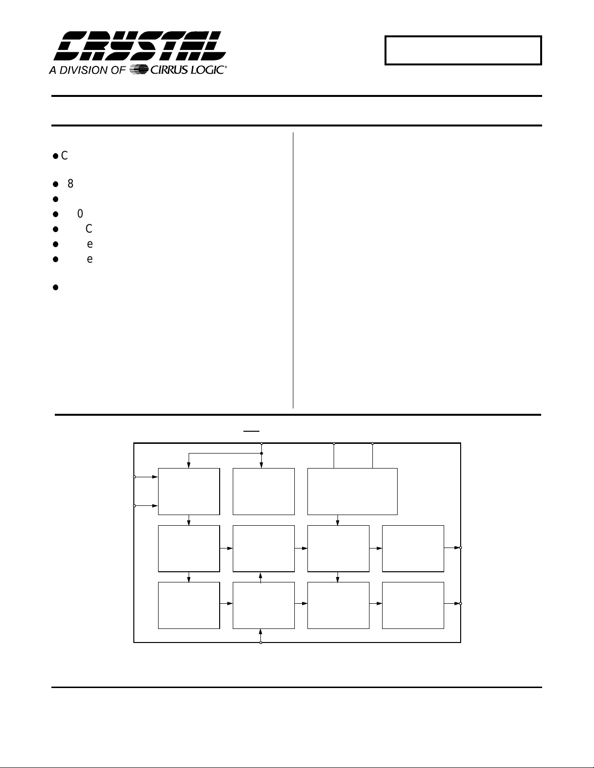
The CS4330, CS4331 and CS4333 are complete , stereo
digital-to-analog output systems including interpolation,
1-bit D/A conversion and output analog filtering in an 8pin package. These devices differ in the serial interface
format used to input audio data.
The CS4330, CS4331 and CS4333 are based on deltasigma modulation, where the modulator output controls
the reference vo lt age input to an ultra-linear analog lowpass filter. Thi s architecture allows for infinite adjustment
of sample rate between 2 kHz and 50 kHz while maintaining linear phase response simply by changing the
master clock frequency.
The CS4330, CS4331 and CS4333 contain on-chip digital de-emphasis, operate from a single +3 V or +5 V
power supply, and consume onl y 60mW o f power with a
3 V power supply. These features make them ideal for
portable CD players and other portable playback
systems.
ORDERING INFORMATION
See page 21.
3
LRCK
SDATA
Cirrus Logic, Inc.
Crystal Semiconductor Products Division
P.O. Box 17847, Austin, Texas 78760
(512) 445 7222 FAX: (512) 445 7581
http://www.crystal.com
1
Serial Input
Interface
Interpolator
Interpolator
DEM/SCLK
2
De-emphasis
Delta-Sigma
Modulator
Delta-Sigma
Modulator
4
MCLK
AGND
6
Voltage Reference
DAC
DAC
Copyright Cirrus Logic, Inc. 1997
(All Rights Reserved)
VA+
7
Analog
Low-Pass
Analog
Low-Pass
Filter
Filter
AOUTL
8
AOUTR
5
MAY ‘97
DS136F1
1
CS4330, CS4331, CS4333
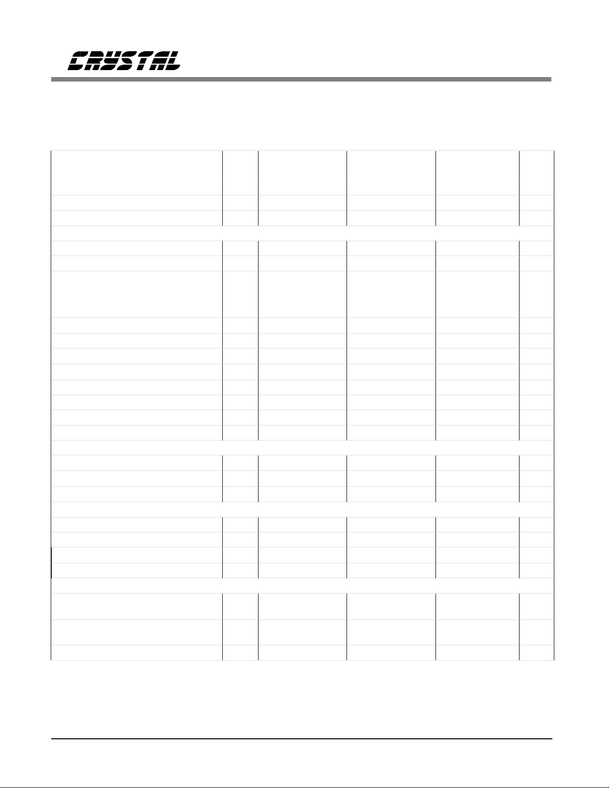
ANALOG CHARACTERISTICS
(TA = 25°C; Logic "1" = VA+; Logic "0" = AGND; MCLK = 12.288 MHz;
Full-Scale Output Sine Wave, 991 Hz; Input Sample Rate = 48 kHz; Input Data = 18 Bits; SCLK = 3.072 MHz;
Measurement Bandwidth is 10 Hz to 20 kHz, unweighted; unless otherwise specified. Resistive load = 20 kΩ, capacitive load = 100 pF)
CS4330/31/33-KS
VA +5V
Parameter Symbol Min Typ Max Min Typ Max Min Typ Max Units
Specified Temperature Range T
Resolution - - 18 - - 18 - - 18 Bits
-10 to 70 -10 to 70 -40 to +85
A
Dynamic Pe rforma nce
Dynamic Range (A-weighted) 90 94 - - 89 - 88 94 - dB
Total Harmonic Distortion - 0.003 0.007 - 0.003 - - .003 .008 %
Total Harmonic Distortion + Noise
0 dB Out put ,
-20 dB Output,
-60 dB Output
Deviation From Linear Phase (Note 1) Passband: to 0.05 dB corner (Note 2,3) 0 to 21.77 0 to 21.77 0 to 21.77 kHz
Frequency Response 10 Hz to 20 kHz(Note 1) Passband Ripple (Note 3) - StopBand (Notes 2,3) 26.23 26.23 26.23 - - kHz
StopBand Attenuation (Note 4) 60 - - 60 - - 60 - - dB
Group Delay (Fs = Input Sample Rate) tgd - 16 / Fs - - 16 / Fs - - 16 / Fs - s
Interchannel Isolation (1 kHz) - 90 - - 90 - - 90 - dB
THD+N
-
-86
-
-72
-
-32
± 0.5
± 0.1
±0.05
dc Accuracy
Interchannel Gain Mismatch - 0.1 - - 0.1 - - 0.1 - dB
Gain Error - Gain Drift - 250 - - 250 - - 250 -
± 10
Analog O utput
Full Scale Output Voltage 3.33 3.70 4.07 1.66 1.85 2.03 3.33 3.70 4.07 Vpp
Output Common Mode Voltage - 2.3 - - 1.3 - - 2.3 - VDC
Minimum Resistive Load - 10 - - 10 - - 20 Maximu m Capa citi ve Load - 100 - - 100 - - 100 - pF
Power Supplies
Power Supply Current: normal operation
power-down
Power Dissipation normal operation
power-down
Power Supply Rejection Ratio (1 kHz) PSRR - 50 - - 50 - - 50 - dB
IA+
IA+
-
28
-
60
-
140
-
160
0.3
CS4330/31/33-KS
-81
-68
-28
--
--
32
-
-
-
-
-
--
--
-
-
-
-
VA +3V
-85
-67
-27
± 0.5
± 0.1
202025
60
0.0675-
CS4330/31/33-BS
-80
-88
-
-
--
--
±0.05
± 10
-
VA +5V only
-86
-
-72
-
-32
± 0.5
± 0.1
--
--
-
-
-
-
±0.05
286032-mA
140
0.3
°C
-79
-66
-26
± 10
160-mW
dB
dB
dB
-deg
-dB
dB
%
ppm/°C
kΩ
µA
mW
Notes: 1. Combined digital and analog filter characteristics.
2. The passband and stopband edges scale with frequency. For input sample rates, Fs, other than
48 kHz, the 0.05 dB passband edge is 0.4535×Fs and the stopband edge is 0.5465×Fs.
3. Digital filte r characteristic s.
4. Measurement Bandwidth is 10 Hz to Fs (kHz)
2 DS136F1
CS4330, CS4331, CS4333
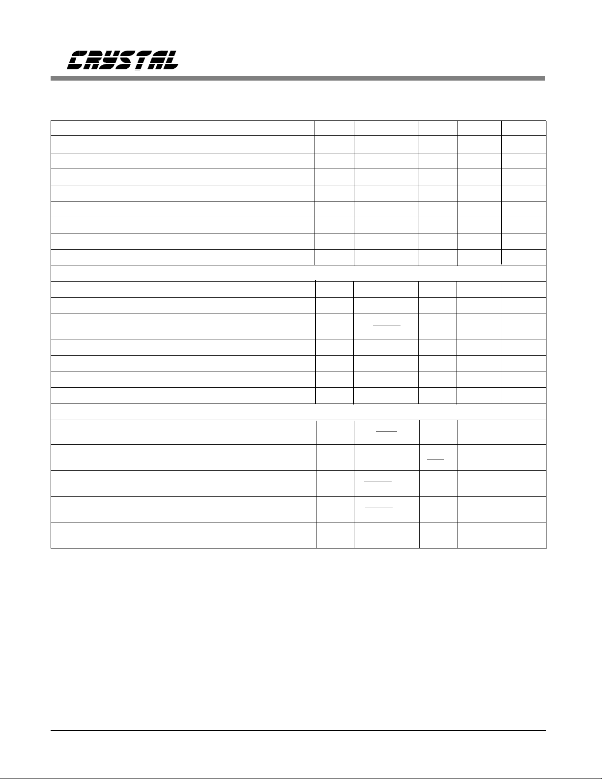
SWITCHING CHARACTERISTICS
(TA = 25 °C; VA+ = 2.7V - 5.5V; Inputs: Logic 0 = 0V, Logic
1 = VA+, CL = 20 pF) Switching characteristics are guaranteed by characterization.
Parameter Symbol Min Typ Max Units
Input Sample Rate Fs 2 - 50 kHz
LRCK Duty Cycle (External SCLK only) (Note 5) 30 50 70 %
MCLK Pulse Width High MCLK / LRCK = 512 10 - 1000 ns
MCLK Pulse Width Low MCLK / LRCK = 512 15 - 1000 ns
MCLK Pulse Width High MCLK / LRCK = 384 21 - 1000 ns
MCLK Pulse Width Low MCLK / LRCK = 384 21 - 1000 ns
MCLK Pulse Width High MCLK / LRCK = 256 35 - 1000 ns
MCLK Pulse Width Low MCLK / LRCK = 256 39 - 1000 ns
External SCLK Mode
SCLK Pulse Width Low t
SCLK Pulse Width High t
SCLK Period t
SCLK rising to LRCK edge delay t
SCLK rising to LRCK edge setup time t
SDATA valid to SCLK rising setup time t
SCLK rising to SDATA hold time t
Internal SCLK Mo de
SCLK Period (Note 6) t
sclkl
sclkh
sclkw
slrd
slrs
sdlrs
sdh
sclkw
20 - - ns
20 - - ns
1
(
128)Fs
--ns
20 - - ns
20 - - ns
20 - - ns
20 - - ns
1
SCLK
--ns
t
SCLK rising to LRCK edge t
SDATA valid to SCLK rising setup time t
SCLK rising to SDATA hold time MCLK / LRCK = 256 or 512 t
SCLK rising to SDATA hold time MCLK / LRCK = 384 t
sclkr -
sdlrs
sdh
sdh
(
(
(
1
512
1
512
1
384
+ 15 --ns
)
Fs
+15 --ns
)
Fs
+15 --ns
)
Fs
sclkw
2
- µs
Notes: 5. In Internal SCLK Mode, the Duty Cycle must be 50% ±1/2 MCLK Peri od.
6. The SCLK / LRCK ratio may be either 32, 48, or 64.
DS136F1 3
LRCK
SCLK
t
slrd
t
slrs
t
sclkl
t
sclkh
CS4330, CS4331, CS4333
SDATA
*LRCK
SDATA
**INTERNAL SCLK
LRCK for CS4331
*
** The SCLK pulses shown are internal to the CS4330/31/33.
t
sdlrs
t
sdh
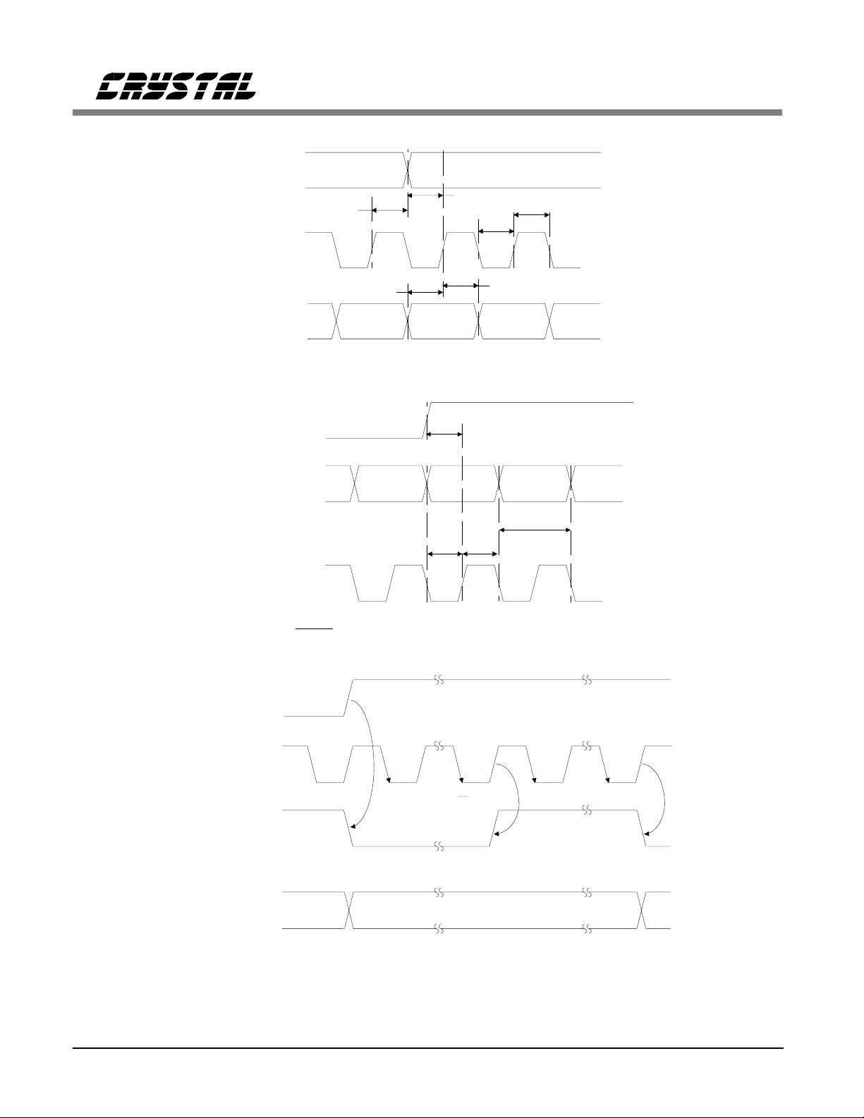
External Serial Mode Input Timing
t
sclkr
t
t
sdlrstsdh
Internal Serial Mode Inp ut Timi ng
sclkw
LRCK
MCLK
*INTERNAL SCLK
SDATA
1
N
2
N
Interna l Ser ial C loc k Gen erati on
* The SCLK pulses shown are internal to the CS4330/31/33.
N equals MCLK divided by SCLK
4 DS136F1
CS4330, CS4331, CS4333
DIGITAL CHARACTERISTICS (TA = 25 °C; VA+ = 2.7V - 5.5V)
Parameter Symbol Min Typ Max Units
High-L eve l I nput Vo ltag e (VA+ = 5. 5V) V
(VA+ = 5.0V) V
Low-Level Input Voltage V
Input Leakage Current (Note 7) I
IH
IH
IL
in
2.4 - - V
2.0 - - V
--0.8V
-- ±10 µA
Notes: 7. Iin for CS4331 LRCK is ± 20 µA max.
ABSOLUTE MAXIMUM RATINGS (AGND = 0V; all voltages with respect to ground.)
Parameter Symbol Min Max Units
DC Power Supply: VA+ -0.3 6.0 V
Input Current, Any Pin Except Supplies I
Digital Input Voltage V
Ambient Operating Temperature (power applied) T
Storage Temperature T
in
IND
A
stg
- ±10 mA
-0.3 (VA+)+0.4 V
-55 125 °C
-65 150 °C
WARNING: Operation at or beyond these limits may result in permanent damage to the device.
Normal operation is not guaranteed at these extremes.
RECOMMENDED OPERATING CONDITIONS ( AGND = 0V; all v oltages with res pect to
ground)
Parameter Symbol Min Typ Max Units
DC Power Supply: (3V mode) VA+ 2.7 3.0 4.0 V
(5V mode) VA+ 4.75 5.0 5.5 V
DS136F1 5
CS4330, CS4331, CS4333
1
Audio
Data
Processor
External Clock MCLK
SDATA
2
DEM/SCLK
3
LRCK
4
VA+
CS4330
CS4331
CS4333
AGND
6
7
AOUTL
AOUTR
2.4k
Ω
2.4k
Ω
+3V/+5V
Ω
**
Ω
**
0.1
µ
F
8
5
µ
10
+
*
10 µF
+
*
+
10 µF
F
56k
*
56k
*
* Required for AC coupling only
** C =
(2
π
1
)(2400Ω)(Fs)(2)
C
C
Left Audio
Output
Right Audio
Output
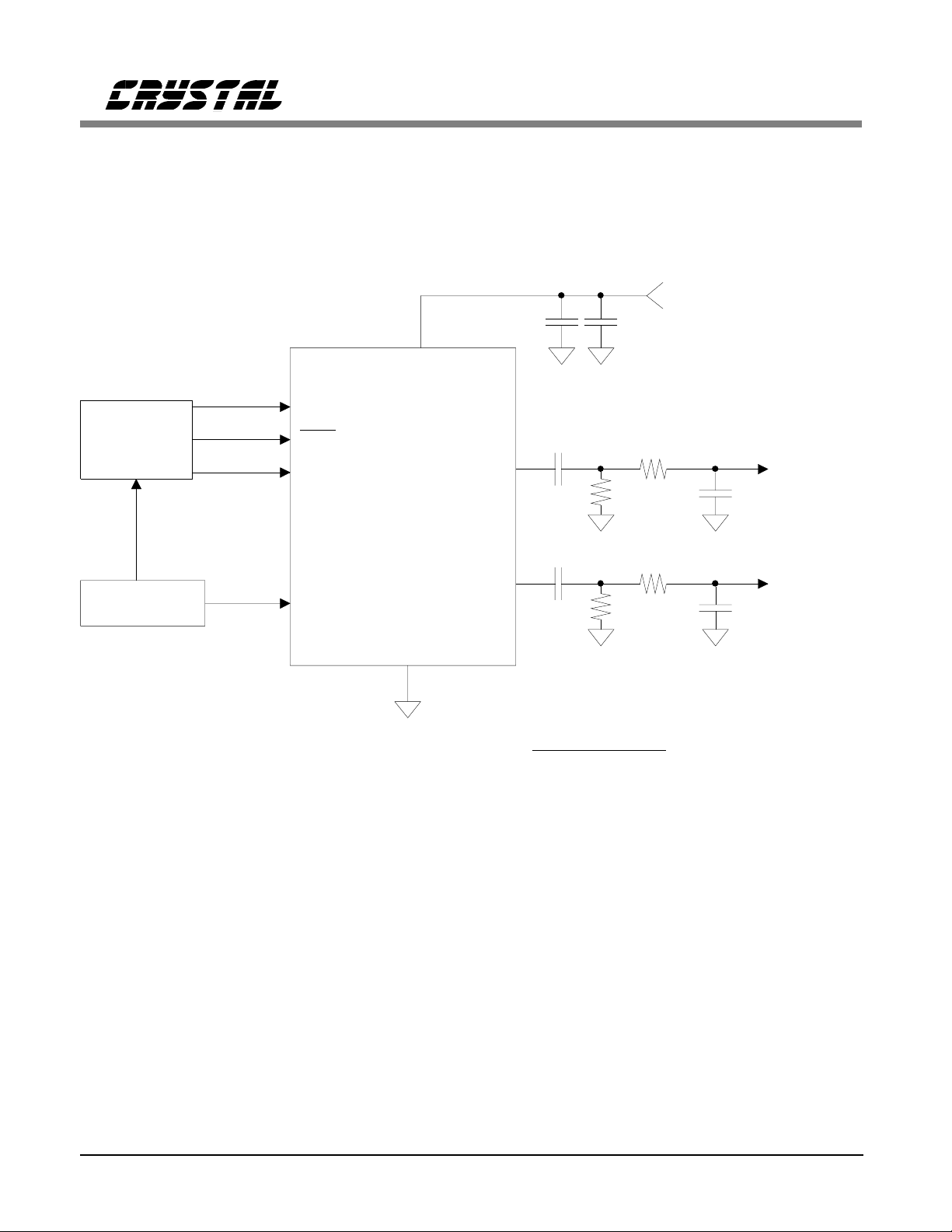
Figure 1. Recommended Connection Diagram
6 DS136F1
CS4330, CS4331, CS4333
GENERAL DESCRIPTION
The CS4330, CS43 31, and CS4333 are co mplete
stereo digital-to-analog systems including digital
interpolation, 128× third-order delta-sigma digital-to-analog co nversion, digital de-emphasis and
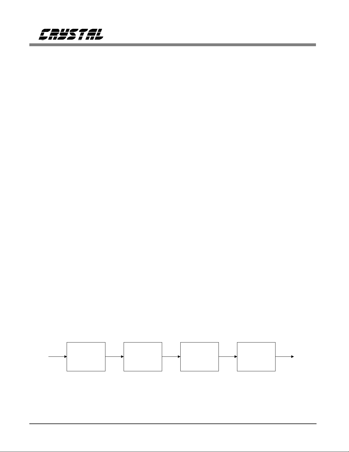
analog filtering, Figure 2. This architecture provides a high tol erance to cl ock jitter.
The primary purpos e of using delta-sigma modulation techniques is to avoid the limitations of
laser trimmed resistive digital-to-analog converter architectures by usin g an inherently linear
1-bit digital-to-analog converter. The advantages
of a 1-bit digital-to-analog converter include:
ideal differential linearity, no distortion mechanisms due to resistor matching errors and no
linearity drift over time and temperature due to
variations in resistor values.
Digital Interpo lation Filter
The digital interp olation filter increases the sample rate by a fact or of 32 an d is followed by a 4×
digital sample-and-hold to effectively achieve a
128× interpolation filter. This filter eliminates
images of the bas eband audio signal which exist
at multiples of the input sample rate, Fs. This
allows for the selection of a less complex analo g
filter based on out-of-band noise attenuation requirements rath er than anti -image filtering.
Following the interpolation filter, the resulting
frequency spectrum has images of the input sig-
nal at multiples of 128× the input sample rate.
These images are removed by the external analog filter.
Delta-Sigma Modula tor
The interpolation filter is followed by a thirdorder delta-sigma modulator which converts the
22-bit interpolation filter output into 1-bit data at
128× .
Switched-Capaci tor Filter
The delta-sigma modulator is followed by a
digital-to-analog converter which translates the
1-bit data into a series of charge packets. The
magnitude of th e charge in each packet is determined by sampling o f a voltage reference onto a
switched capacitor, where the polarity of each
packet is controlled by the 1-bit signal. This
technique gre atly reduces the sensitivity to clock
jitter and is a major improvement over earlier
generations of 1 -bit digital-to -analog converters.
Digital
Input
DS136F1 7
Interpolato r
Delta-Sigma
Modulator
Figure 2. System Block Diagram
DAC
Analog
Low-Pass
Filter
Analog
Output
CS4330, CS4331, CS4333
SYSTEM DESIGN
The CS4330/31/ 33 accept data at standard a udio
frequencies including 48 kHz, 44.1 kHz and
32 kHz. Audio data is input via the serial data
input pin (SDATA). The Left/Right Clock
(LRCK) defines the channel and delineation of
data and the Serial Clock (SCLK) clocks audio
data into the input data buffer. The CS4330,
CS4331 and CS43 33 differ in the serial data format as shown in Figures 4-7. The Master Clock
(MCLK) is used to operate the digital interpolation filter and the d elta-sigma modulator.
Master Clock
The MCLK must be either 256×, 384×, or 512×
the desired input sample rate, Fs. Fs is the frequency at which words for each channel are
input to the digital-to-analog converter, and is
equal to the LRCK frequency. The MCLK to
LRCK frequency ratio is detected automatically
during the initialization sequence by counting
the number of MC LK transitions during a single
LRCK period. Internal dividers are set to generate the proper clocks for the digital filter,
delta-sigma modulator and switched-capacitor
filter. Table 1 illustrates several standard audio
sample rates and t he required MCLK and LRCK
frequencie s.
LRCK
(kHz)
32 8.1920 12.2880 16.3840
44.1 11.2896 16.9344 22.5792
48 12.2880 18.4320 24.5760
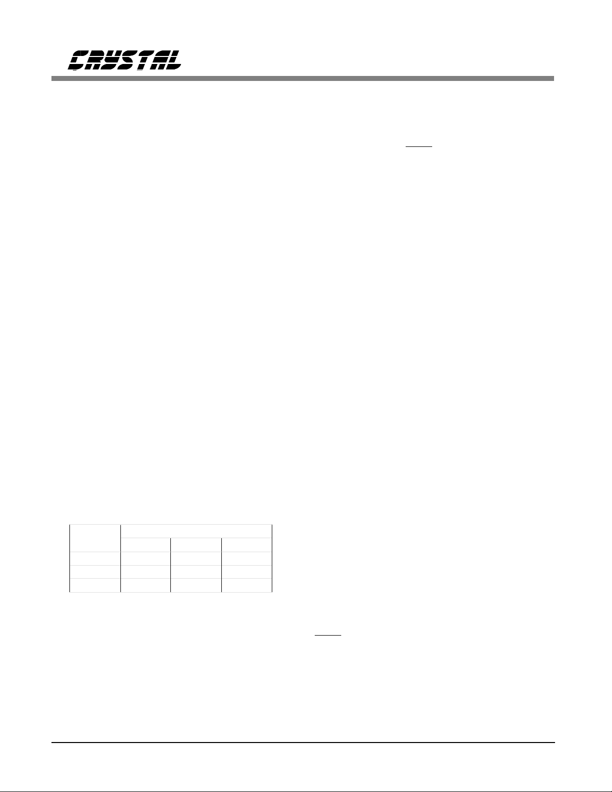
Table 1. Common Clock Frequencies
256x 384x 512x
MCLK (MHz)
External Seria l Clock Mode
The CS4330/31/33 will enter the External Serial
Clock Mode when 4 low to high transitions are
detected on the
DEM/SCLK pin during any
phase of the LRCK period. When this mode is
enabled, the Internal Serial Clock Mode an d deemphasis filter cannot be accessed. The
CS4330/31/33 must return to Power-Down to
exit this mode. Refer to Fi gure 8.
Internal Serial C lock Mode
In the Internal Serial Clock Mode, the serial
clock is internall y derived and synchronou s with
MCLK and LRCK. The SCLK/LRCK frequency
ratio is either 32, 48, or 64. Operation in this
mode is identical to operation with an external
serial clock synchronized with LRCK. This
mode allows access to the digital de-emphasis
function. Refer to Figure 8 .
While the Internal Serial Clock Mode is provided to allow access to the de-emphasis filter,
the Internal Serial Clock Mode also eliminates
possible clock interference from an external
SCLK. Use of Internal Serial Clock Mode is always preferred, even when de-emphasis filtering
is not required.
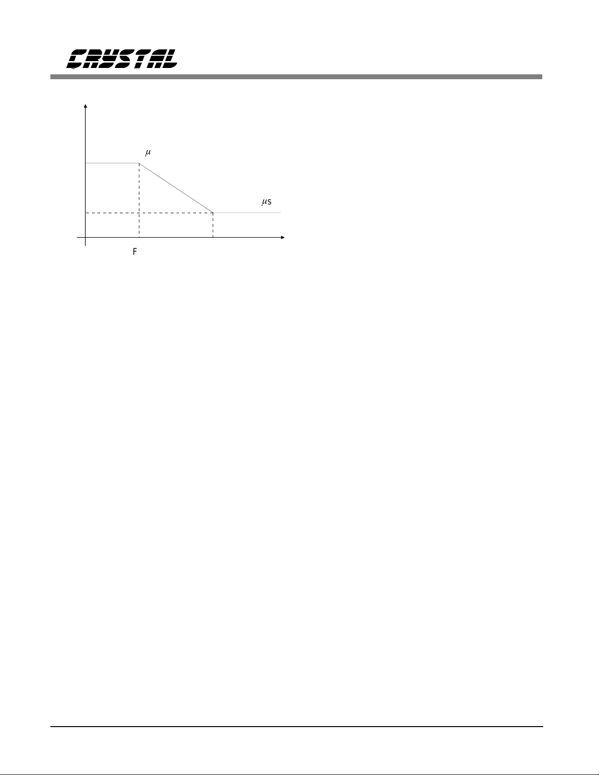
De-Emphasis
The CS4330/31/33 include on-chip digital deemphasis. Figure 3 shows the de-emphasis curve
for Fs equal to 44.1 kHz. The frequency response of the de-emphasis curve will scale
proportional ly with changes in sample rate, Fs.
Serial Clock
The de-emphasis filter is active (inactive) if the
DEM/SCLK pin is low (high) for 8 consecutive
The serial clock co ntrols the shifting o f data into
the input data buffers. The CS4330/31/33 sup-
falling edges of L RCK. This functi on is available
only in th e internal serial clo ck mode.
port both external and internal serial clock
generation modes. Refer to Figures 4-7 for data
formats.
8 DS136F1
Gain
dB
0dB
T1=50
CS4330, CS4331, CS4333
CS4330/31/3 3 adapt to these new operating conditions. It is recomended that the CS4330/31/33
not be powered up with the clocks (MCLK,
LRCK, SCLK) going.
m
s
Power Supply Determination
m
T2 = 15
-10dB
F1 F2
3.183 kHz 10.61 kHz
Figure 3. De-Emphas is Curve (Fs = 44.1kHz)
s
Frequency
Initializatio n and Power-Down
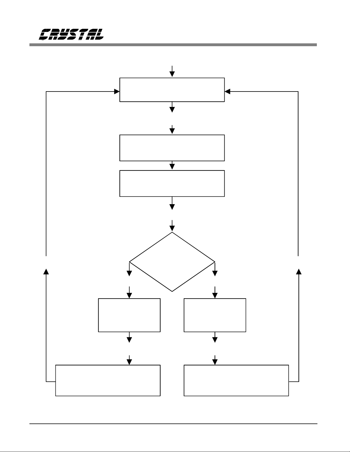
The Initialization and Power-Down sequence
flow chart is shown in Figure 8. The CS4330/31/33
enter the Power-Down mode upon initial powerup. The interpolation filters and delta-sigma
modulators are reset, and the interna l voltage reference, one-bit digital-to-analog converters and
switched-capacitor low-pass filters are powered
down. The device will remain in the PowerDown mode until MCLK and LRCK are
presented. Once MCLK and LRCK are detect ed,
MCLK occurrence s are counted over one LRCK
period to determine the MCL K/LRCK frequency
ratio. Power is then applied to the internal voltage reference and the +5 or +3 Volt power
supply mode is determined. Finally, power is
applied to the D/A converters and switched-capacitor filters, and the analog outputs will move
to approximately 2.3V (1.3V in 3V mode). This
process requires approximately 1ms plus 1024
cycl es of LRC K.
The nominal power supply voltage for the
CS4330/31/33 may be either +5 or +3 Volts.
"SMART Analog" circuitry senses the power
supply voltage during the initialization sequence
or when exiting th e Power-Down mode. +5V operation will be set with a 3.7 Vpp full scale
output if VA+ is b etween 4.75 and 5.5 Volts. The
CS4330/31/3 3 will b e set for +3V o peration wi th
a 1.85 Vpp full scale output if VA+ is between
2.7 and 4.0 Volts. Supply voltages between 4.0
and 4.75 Volts should be avoided to prevent operation in the 5V mode. In this conditio n there is
insufficient headroom to pr oduce a 3.7 Vpp output.
Grounding and Power Supply Decoupling
As with any high resolution converter, the
CS4330/31/33 require careful attention to power
supply and grounding arrangements to optimize
performance. Figure 1 shows the recommended
power arrangements with VA+ connected to a
clean +3/+5V supply. Decoupling capacitors
should be located as near to the CS4330/31/33
as possible.
Analog Output and Filtering
The CS4330/3 1/33 analog filter is a switched -capacitor filter. The switched-capacitor filter
frequency response is clock dependent and will
scale with sample rate.
The CS4330/31/33 enter the Power-Down mode
within 1 period of LRCK if either MCLK or
LRCK is removed. The initialization sequence
begins when MCLK and LRCK are restored. If
the MCLK/LRCK frequency ratio or the VA+
voltage changes during Power-Down, the
DS136F1 9
The digital filter of the CS4330/31/33 is designed to compensate for the magnitude and
phase resp onse of a single-pole low-pass filter at
twice the sample rate . Output filters consisting of
a 2.4 kohm resistor and capacitor are recom-
CS4330, CS4331, CS4333
LRCK
SCLK
SDATA
10
17 16 17 16
Left Channel
15 14 13 12 11 10
Inter nal SCLK Mode
Right Justified, 18-Bit Data
Data Valid on Rising Edge of SCLK
INT SCLK = 64 Fs if MCLK/LRCK = 256 or 512
INT SCLK = 48 Fs if MCLK/LRCK = 3 84
6543210987
External SCLK Mode
Right Justified, 18-Bit Data
Data Valid on Rising Edge of SCLK
SCLK must have at least 36 cycles per LRCK
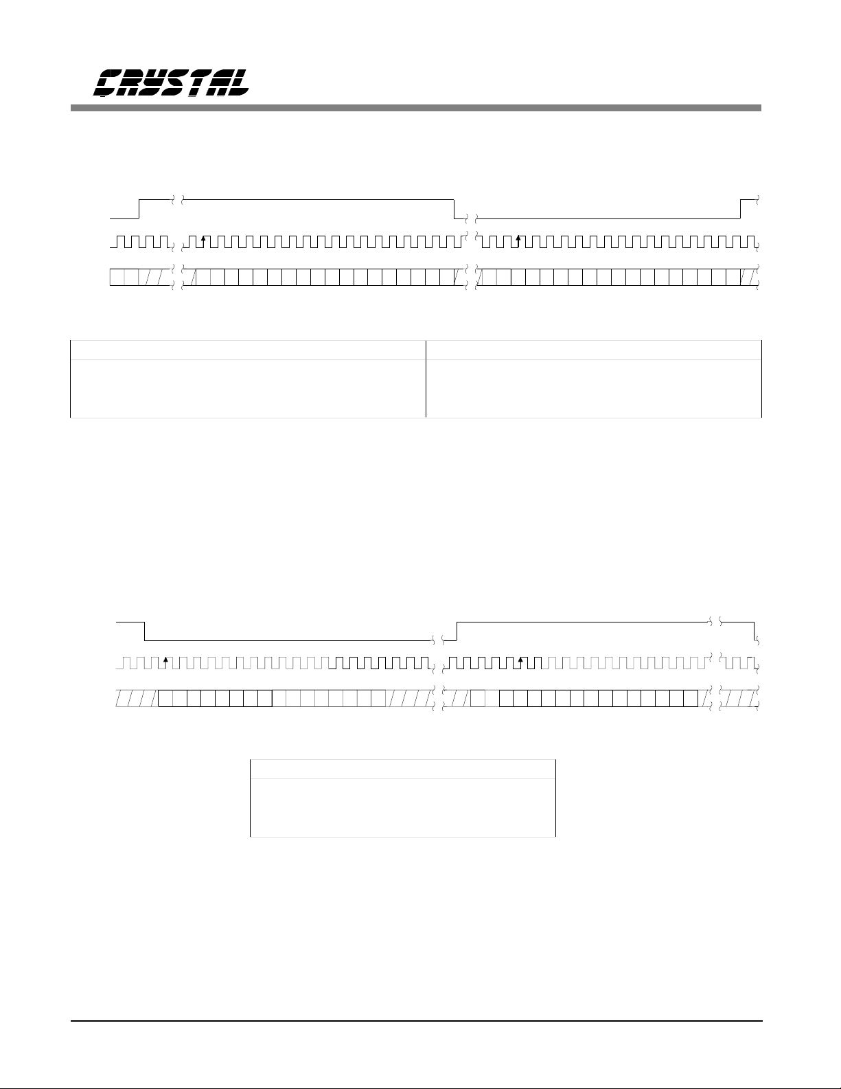
Figure 4. CS4330 Data Format
Right Chan nel
15 14 13 12 11 10
6543210987
LRCK
SCLK
SDATA 6543210987
15 14 13 12 11 10
Left Channel
Inter nal SCLK Mode
I2S, 16-Bit Data
Data Valid on Rising Edge of SCLK
INT SCLK = 32 Fs if MCLK/LRCK = 512 or 256
INT SCLK = 48 Fs if MCLK/LRCK = 3 84
Figure 5. CS4331 Internal SCLK Data Format (I2S)
15 14 13 12 11 10
Right Channel
6543210987
10 DS136F1
CS4330, CS4331, CS4333
LRCK
SCLK
SDATA
Left Channel
654321098715 14 13 12 11 1017 16 654321098715 14 13 12 11 1017 16
External SCLK Mode
I2S, 18-Bit Data
Data Valid on Rising Edge of SCLK
SCLK must have at least 36 cycles per LRCK
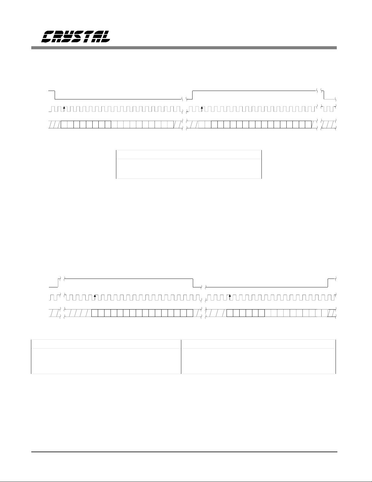
Figure 6. CS4331 External SCLK Data Format (I2S)
Right Channel
LRCK
SCLK
SDATA
Left Channel
15 14 13 12 11 10
Inter nal SCLK Mode
Right Justified, 16-Bit Data
Data Valid on Rising Edge of SCLK
INT SCLK = 32 Fs if MCLK/LRCK = 512 or 256
6543210987
15 14 13 12 11 10
External SCLK Mode
Right Justified, 16-Bit Data
Data Valid on Rising Edge of SCLK
SCLK must have at least 32 cycles per LRCK
Right Channel
6543210987
INT SCLK = 48 Fs if MCLK/LRCK = 3 84
Figure 7. CS4333 SCLK Data Format
DS136F1 11
USER: Apply Power
Power-Down Mode
USER: Apply MCLK and LRCK
256/384/512
MCLK/LRCK Determination
Power Supply Determination
+3 or +5 Volt mode
CS4330, CS4331, CS4333
USER: set SCLK mode
Normal Operation
De-emphasis
available
USER: Apply SDATA
Analog Output
is Generated
SCLK mode
Normal Operation
USER: Apply SDATA
USER: Remove ClocksUSER: Remove Clocks
externalinternal
De-emphasis
not available
Analog Output
is Generated
Figure 8. CS4330/31/33 Initialization and Power-Down Sequence
12 DS136F1
 Loading...