

CS4330/31/33
8 Pin Stereo D/A Converter for Digital Audio
Features
l
Complete Stereo DAC System:
Interpolation, D/A, Output Analog Filtering
l
18-Bit Resolution
l
94 dB Dynamic Range
l
0.003% THD
l
Low Clock Jitter Sensitivity
l
Single +3 V or +5 V Power Supply
l
Filtered Line Level Outputs
Linear Phase Filtering
l
On-Chip Digital De-emphasis
I
Description
The CS4330, CS4331 and CS4333 are complete , stereo
digital-to-analog output systems including interpolation,
1-bit D/A conversion and output analog filtering in an 8pin package. These devices differ in the serial interface
format used to input audio data.
The CS4330, CS4331 and CS4333 are based on deltasigma modulation, where the modulator output controls
the reference vo lt age input to an ultra-linear analog lowpass filter. Thi s architecture allows for infinite adjustment
of sample rate between 2 kHz and 50 kHz while maintaining linear phase response simply by changing the
master clock frequency.
The CS4330, CS4331 and CS4333 contain on-chip digital de-emphasis, operate from a single +3 V or +5 V
power supply, and consume onl y 60mW o f power with a
3 V power supply. These features make them ideal for
portable CD players and other portable playback
systems.
ORDERING INFORMATION
See page 21.
3
LRCK
SDATA
Cirrus Logic, Inc.
Crystal Semiconductor Products Division
P.O. Box 17847, Austin, Texas 78760
(512) 445 7222 FAX: (512) 445 7581
http://www.crystal.com
1
Serial Input
Interface
Interpolator
Interpolator
DEM/SCLK
2
De-emphasis
Delta-Sigma
Modulator
Delta-Sigma
Modulator
4
MCLK
AGND
6
Voltage Reference
DAC
DAC
Copyright Cirrus Logic, Inc. 1997
(All Rights Reserved)
VA+
7
Analog
Low-Pass
Analog
Low-Pass
Filter
Filter
AOUTL
8
AOUTR
5
MAY ‘97
DS136F1
1
CS4330, CS4331, CS4333
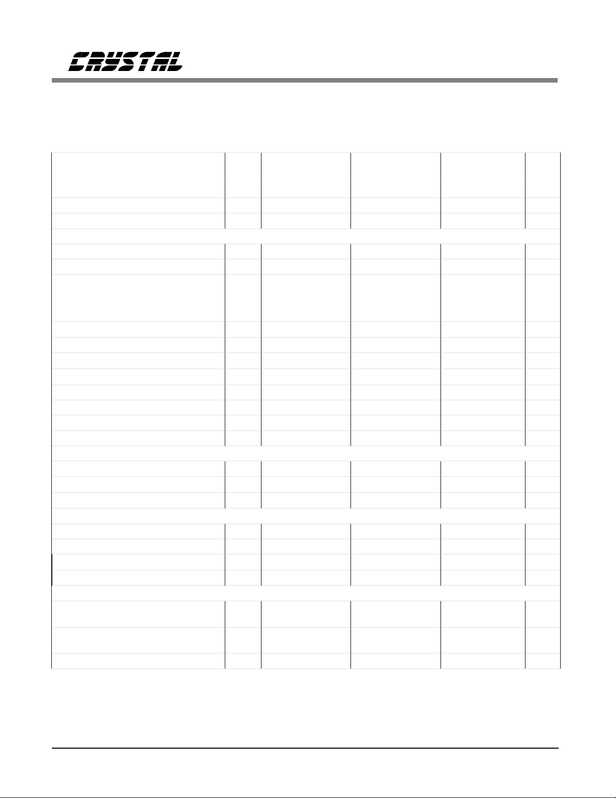
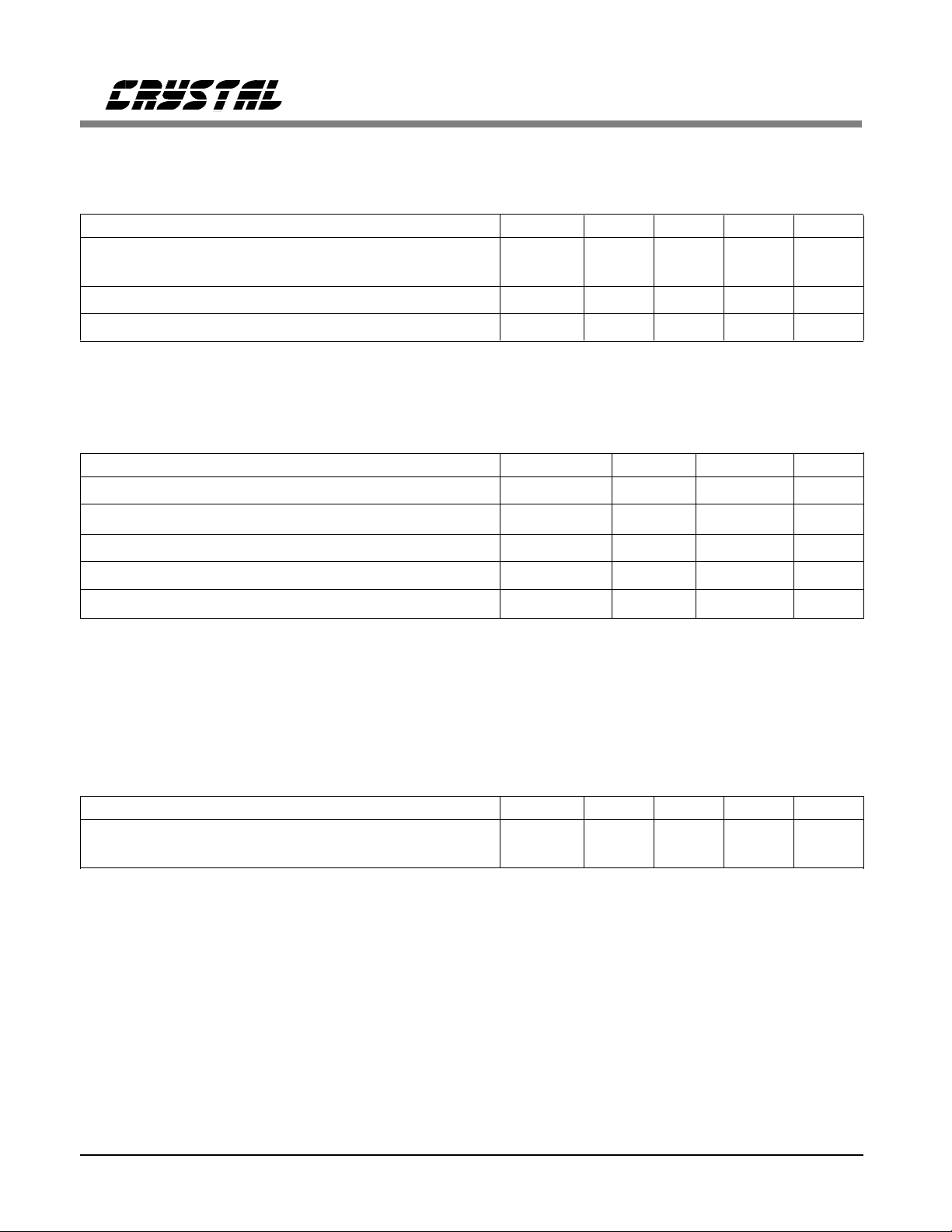
ANALOG CHARACTERISTICS
(TA = 25°C; Logic "1" = VA+; Logic "0" = AGND; MCLK = 12.288 MHz;
Full-Scale Output Sine Wave, 991 Hz; Input Sample Rate = 48 kHz; Input Data = 18 Bits; SCLK = 3.072 MHz;
Measurement Bandwidth is 10 Hz to 20 kHz, unweighted; unless otherwise specified. Resistive load = 20 kΩ, capacitive load = 100 pF)
CS4330/31/33-KS
VA +5V
Parameter Symbol Min Typ Max Min Typ Max Min Typ Max Units
Specified Temperature Range T
Resolution - - 18 - - 18 - - 18 Bits
-10 to 70 -10 to 70 -40 to +85
A
Dynamic Pe rforma nce
Dynamic Range (A-weighted) 90 94 - - 89 - 88 94 - dB
Total Harmonic Distortion - 0.003 0.007 - 0.003 - - .003 .008 %
Total Harmonic Distortion + Noise
0 dB Out put ,
-20 dB Output,
-60 dB Output
Deviation From Linear Phase (Note 1) Passband: to 0.05 dB corner (Note 2,3) 0 to 21.77 0 to 21.77 0 to 21.77 kHz
Frequency Response 10 Hz to 20 kHz(Note 1) Passband Ripple (Note 3) - StopBand (Notes 2,3) 26.23 26.23 26.23 - - kHz
StopBand Attenuation (Note 4) 60 - - 60 - - 60 - - dB
Group Delay (Fs = Input Sample Rate) tgd - 16 / Fs - - 16 / Fs - - 16 / Fs - s
Interchannel Isolation (1 kHz) - 90 - - 90 - - 90 - dB
THD+N
-
-86
-
-72
-
-32
± 0.5
± 0.1
±0.05
dc Accuracy
Interchannel Gain Mismatch - 0.1 - - 0.1 - - 0.1 - dB
Gain Error - Gain Drift - 250 - - 250 - - 250 -
± 10
Analog O utput
Full Scale Output Voltage 3.33 3.70 4.07 1.66 1.85 2.03 3.33 3.70 4.07 Vpp
Output Common Mode Voltage - 2.3 - - 1.3 - - 2.3 - VDC
Minimum Resistive Load - 10 - - 10 - - 20 Maximu m Capa citi ve Load - 100 - - 100 - - 100 - pF
Power Supplies
Power Supply Current: normal operation
power-down
Power Dissipation normal operation
power-down
Power Supply Rejection Ratio (1 kHz) PSRR - 50 - - 50 - - 50 - dB
IA+
IA+
-
28
-
60
-
140
-
160
0.3
CS4330/31/33-KS
-81
-68
-28
--
--
32
-
-
-
-
-
--
--
-
-
-
-
VA +3V
-85
-67
-27
± 0.5
± 0.1
202025
60
0.0675-
CS4330/31/33-BS
-80
-88
-
-
--
--
±0.05
± 10
-
VA +5V only
-86
-
-72
-
-32
± 0.5
± 0.1
--
--
-
-
-
-
±0.05
286032-mA
140
0.3
°C
-79
-66
-26
± 10
160-mW
dB
dB
dB
-deg
-dB
dB
%
ppm/°C
kΩ
µA
mW
Notes: 1. Combined digital and analog filter characteristics.
2. The passband and stopband edges scale with frequency. For input sample rates, Fs, other than
48 kHz, the 0.05 dB passband edge is 0.4535×Fs and the stopband edge is 0.5465×Fs.
3. Digital filte r characteristic s.
4. Measurement Bandwidth is 10 Hz to Fs (kHz)
2 DS136F1
CS4330, CS4331, CS4333
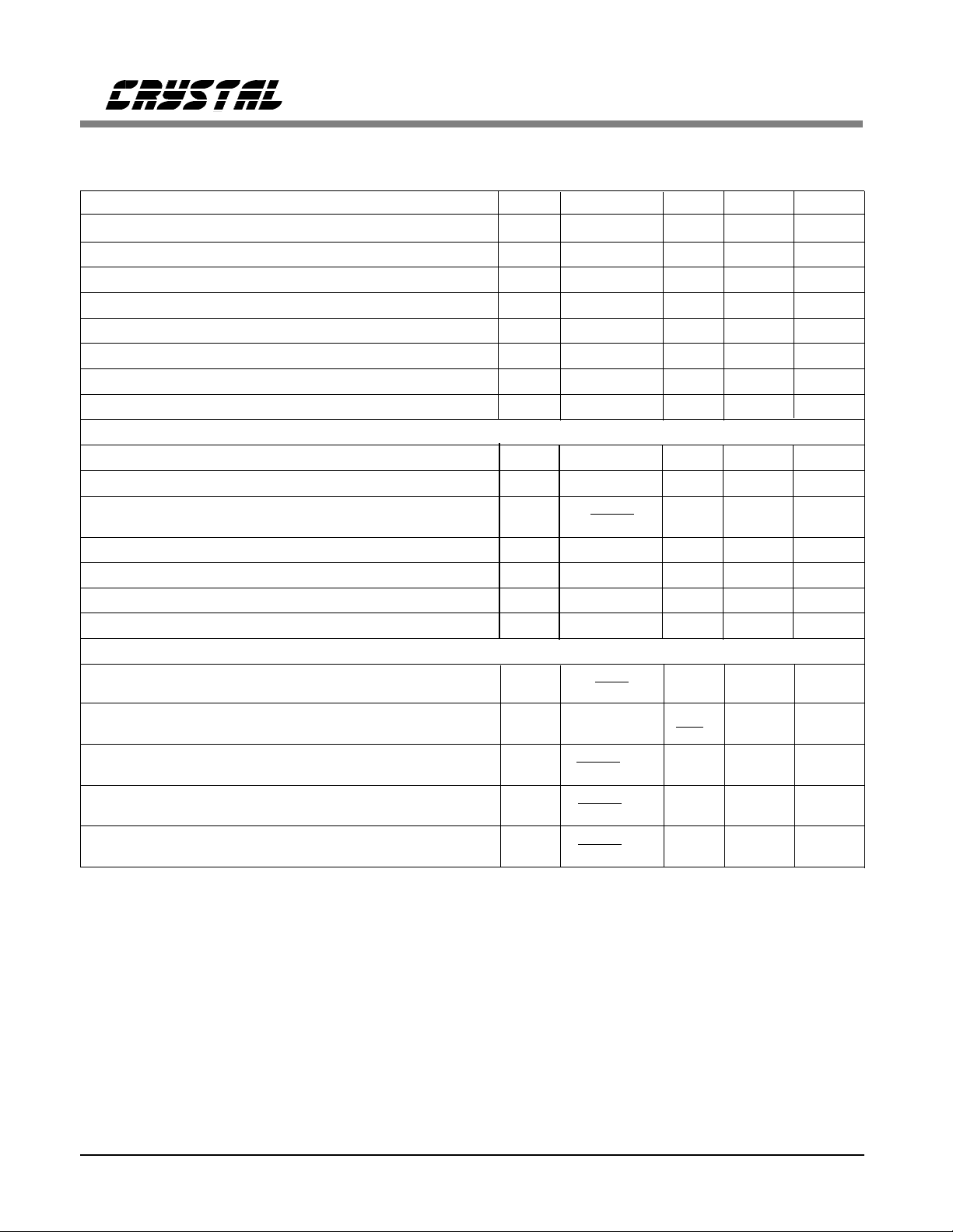
SWITCHING CHARACTERISTICS
(TA = 25 °C; VA+ = 2.7V - 5.5V; Inputs: Logic 0 = 0V, Logic
1 = VA+, CL = 20 pF) Switching characteristics are guaranteed by characterization.
Parameter Symbol Min Typ Max Units
Input Sample Rate Fs 2 - 50 kHz
LRCK Duty Cycle (External SCLK only) (Note 5) 30 50 70 %
MCLK Pulse Width High MCLK / LRCK = 512 10 - 1000 ns
MCLK Pulse Width Low MCLK / LRCK = 512 15 - 1000 ns
MCLK Pulse Width High MCLK / LRCK = 384 21 - 1000 ns
MCLK Pulse Width Low MCLK / LRCK = 384 21 - 1000 ns
MCLK Pulse Width High MCLK / LRCK = 256 35 - 1000 ns
MCLK Pulse Width Low MCLK / LRCK = 256 39 - 1000 ns
External SCLK Mode
SCLK Pulse Width Low t
SCLK Pulse Width High t
SCLK Period t
SCLK rising to LRCK edge delay t
SCLK rising to LRCK edge setup time t
SDATA valid to SCLK rising setup time t
SCLK rising to SDATA hold time t
Internal SCLK Mo de
SCLK Period (Note 6) t
sclkl
sclkh
sclkw
slrd
slrs
sdlrs
sdh
sclkw
20 - - ns
20 - - ns
1
(
128)Fs
--ns
20 - - ns
20 - - ns
20 - - ns
20 - - ns
1
SCLK
--ns
t
SCLK rising to LRCK edge t
SDATA valid to SCLK rising setup time t
SCLK rising to SDATA hold time MCLK / LRCK = 256 or 512 t
SCLK rising to SDATA hold time MCLK / LRCK = 384 t
sclkr -
sdlrs
sdh
sdh
(
(
(
1
512
1
512
1
384
+ 15 --ns
)
Fs
+15 --ns
)
Fs
+15 --ns
)
Fs
sclkw
2
- µs
Notes: 5. In Internal SCLK Mode, the Duty Cycle must be 50% ±1/2 MCLK Peri od.
6. The SCLK / LRCK ratio may be either 32, 48, or 64.
DS136F1 3
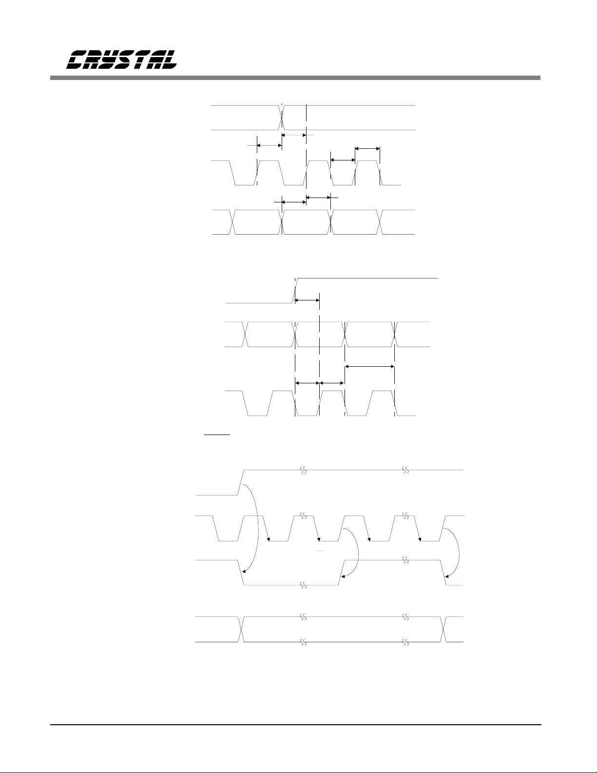
LRCK
SCLK
t
slrd
t
slrs
t
sclkl
t
sclkh
CS4330, CS4331, CS4333
SDATA
*LRCK
SDATA
**INTERNAL SCLK
LRCK for CS4331
*
** The SCLK pulses shown are internal to the CS4330/31/33.
t
sdlrs
t
sdh
External Serial Mode Input Timing
t
sclkr
t
t
sdlrstsdh
Internal Serial Mode Inp ut Timi ng
sclkw
LRCK
MCLK
*INTERNAL SCLK
SDATA
1
N
2
N
Interna l Ser ial C loc k Gen erati on
* The SCLK pulses shown are internal to the CS4330/31/33.
N equals MCLK divided by SCLK
4 DS136F1
CS4330, CS4331, CS4333
DIGITAL CHARACTERISTICS (TA = 25 °C; VA+ = 2.7V - 5.5V)
Parameter Symbol Min Typ Max Units
High-L eve l I nput Vo ltag e (VA+ = 5. 5V) V
(VA+ = 5.0V) V
Low-Level Input Voltage V
Input Leakage Current (Note 7) I
IH
IH
IL
in
2.4 - - V
2.0 - - V
--0.8V
-- ±10 µA
Notes: 7. Iin for CS4331 LRCK is ± 20 µA max.
ABSOLUTE MAXIMUM RATINGS (AGND = 0V; all voltages with respect to ground.)
Parameter Symbol Min Max Units
DC Power Supply: VA+ -0.3 6.0 V
Input Current, Any Pin Except Supplies I
Digital Input Voltage V
Ambient Operating Temperature (power applied) T
Storage Temperature T
in
IND
A
stg
- ±10 mA
-0.3 (VA+)+0.4 V
-55 125 °C
-65 150 °C
WARNING: Operation at or beyond these limits may result in permanent damage to the device.
Normal operation is not guaranteed at these extremes.
RECOMMENDED OPERATING CONDITIONS ( AGND = 0V; all v oltages with res pect to
ground)
Parameter Symbol Min Typ Max Units
DC Power Supply: (3V mode) VA+ 2.7 3.0 4.0 V
(5V mode) VA+ 4.75 5.0 5.5 V
DS136F1 5
CS4330, CS4331, CS4333
1
Audio
Data
Processor
External Clock MCLK
SDATA
2
DEM/SCLK
3
LRCK
4
VA+
CS4330
CS4331
CS4333
AGND
6
7
AOUTL
AOUTR
2.4k
Ω
2.4k
Ω
+3V/+5V
Ω
**
Ω
**
0.1
µ
F
8
5
µ
10
+
*
10 µF
+
*
+
10 µF
F
56k
*
56k
*
* Required for AC coupling only
** C =
(2
π
1
)(2400Ω)(Fs)(2)
C
C
Left Audio
Output
Right Audio
Output
Figure 1. Recommended Connection Diagram
6 DS136F1
CS4330, CS4331, CS4333
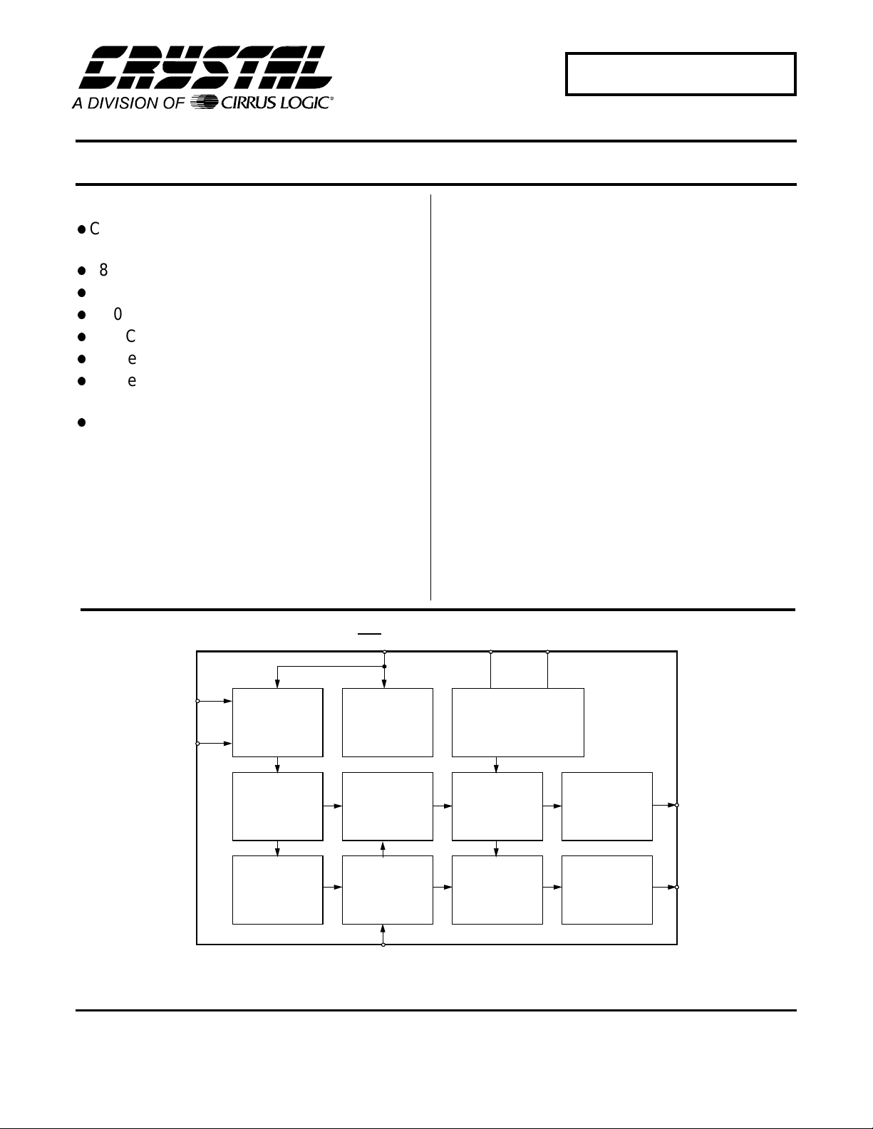
GENERAL DESCRIPTION
The CS4330, CS43 31, and CS4333 are co mplete
stereo digital-to-analog systems including digital
interpolation, 128× third-order delta-sigma digital-to-analog co nversion, digital de-emphasis and
analog filtering, Figure 2. This architecture provides a high tol erance to cl ock jitter.
The primary purpos e of using delta-sigma modulation techniques is to avoid the limitations of
laser trimmed resistive digital-to-analog converter architectures by usin g an inherently linear
1-bit digital-to-analog converter. The advantages
of a 1-bit digital-to-analog converter include:
ideal differential linearity, no distortion mechanisms due to resistor matching errors and no
linearity drift over time and temperature due to
variations in resistor values.
Digital Interpo lation Filter
The digital interp olation filter increases the sample rate by a fact or of 32 an d is followed by a 4×
digital sample-and-hold to effectively achieve a
128× interpolation filter. This filter eliminates
images of the bas eband audio signal which exist
at multiples of the input sample rate, Fs. This
allows for the selection of a less complex analo g
filter based on out-of-band noise attenuation requirements rath er than anti -image filtering.
Following the interpolation filter, the resulting
frequency spectrum has images of the input sig-
nal at multiples of 128× the input sample rate.
These images are removed by the external analog filter.
Delta-Sigma Modula tor
The interpolation filter is followed by a thirdorder delta-sigma modulator which converts the
22-bit interpolation filter output into 1-bit data at
128× .
Switched-Capaci tor Filter
The delta-sigma modulator is followed by a
digital-to-analog converter which translates the
1-bit data into a series of charge packets. The
magnitude of th e charge in each packet is determined by sampling o f a voltage reference onto a
switched capacitor, where the polarity of each
packet is controlled by the 1-bit signal. This
technique gre atly reduces the sensitivity to clock
jitter and is a major improvement over earlier
generations of 1 -bit digital-to -analog converters.
Digital
Input
DS136F1 7
Interpolato r
Delta-Sigma
Modulator
Figure 2. System Block Diagram
DAC
Analog
Low-Pass
Filter
Analog
Output
CS4330, CS4331, CS4333
SYSTEM DESIGN
The CS4330/31/ 33 accept data at standard a udio
frequencies including 48 kHz, 44.1 kHz and
32 kHz. Audio data is input via the serial data
input pin (SDATA). The Left/Right Clock
(LRCK) defines the channel and delineation of
data and the Serial Clock (SCLK) clocks audio
data into the input data buffer. The CS4330,
CS4331 and CS43 33 differ in the serial data format as shown in Figures 4-7. The Master Clock
(MCLK) is used to operate the digital interpolation filter and the d elta-sigma modulator.
Master Clock
The MCLK must be either 256×, 384×, or 512×
the desired input sample rate, Fs. Fs is the frequency at which words for each channel are
input to the digital-to-analog converter, and is
equal to the LRCK frequency. The MCLK to
LRCK frequency ratio is detected automatically
during the initialization sequence by counting
the number of MC LK transitions during a single
LRCK period. Internal dividers are set to generate the proper clocks for the digital filter,
delta-sigma modulator and switched-capacitor
filter. Table 1 illustrates several standard audio
sample rates and t he required MCLK and LRCK
frequencie s.
LRCK
(kHz)
32 8.1920 12.2880 16.3840
44.1 11.2896 16.9344 22.5792
48 12.2880 18.4320 24.5760
Table 1. Common Clock Frequencies
256x 384x 512x
MCLK (MHz)
External Seria l Clock Mode
The CS4330/31/33 will enter the External Serial
Clock Mode when 4 low to high transitions are
detected on the
DEM/SCLK pin during any
phase of the LRCK period. When this mode is
enabled, the Internal Serial Clock Mode an d deemphasis filter cannot be accessed. The
CS4330/31/33 must return to Power-Down to
exit this mode. Refer to Fi gure 8.
Internal Serial C lock Mode
In the Internal Serial Clock Mode, the serial
clock is internall y derived and synchronou s with
MCLK and LRCK. The SCLK/LRCK frequency
ratio is either 32, 48, or 64. Operation in this
mode is identical to operation with an external
serial clock synchronized with LRCK. This
mode allows access to the digital de-emphasis
function. Refer to Figure 8 .
While the Internal Serial Clock Mode is provided to allow access to the de-emphasis filter,
the Internal Serial Clock Mode also eliminates
possible clock interference from an external
SCLK. Use of Internal Serial Clock Mode is always preferred, even when de-emphasis filtering
is not required.
De-Emphasis
The CS4330/31/33 include on-chip digital deemphasis. Figure 3 shows the de-emphasis curve
for Fs equal to 44.1 kHz. The frequency response of the de-emphasis curve will scale
proportional ly with changes in sample rate, Fs.
Serial Clock
The de-emphasis filter is active (inactive) if the
DEM/SCLK pin is low (high) for 8 consecutive
The serial clock co ntrols the shifting o f data into
the input data buffers. The CS4330/31/33 sup-
falling edges of L RCK. This functi on is available
only in th e internal serial clo ck mode.
port both external and internal serial clock
generation modes. Refer to Figures 4-7 for data
formats.
8 DS136F1
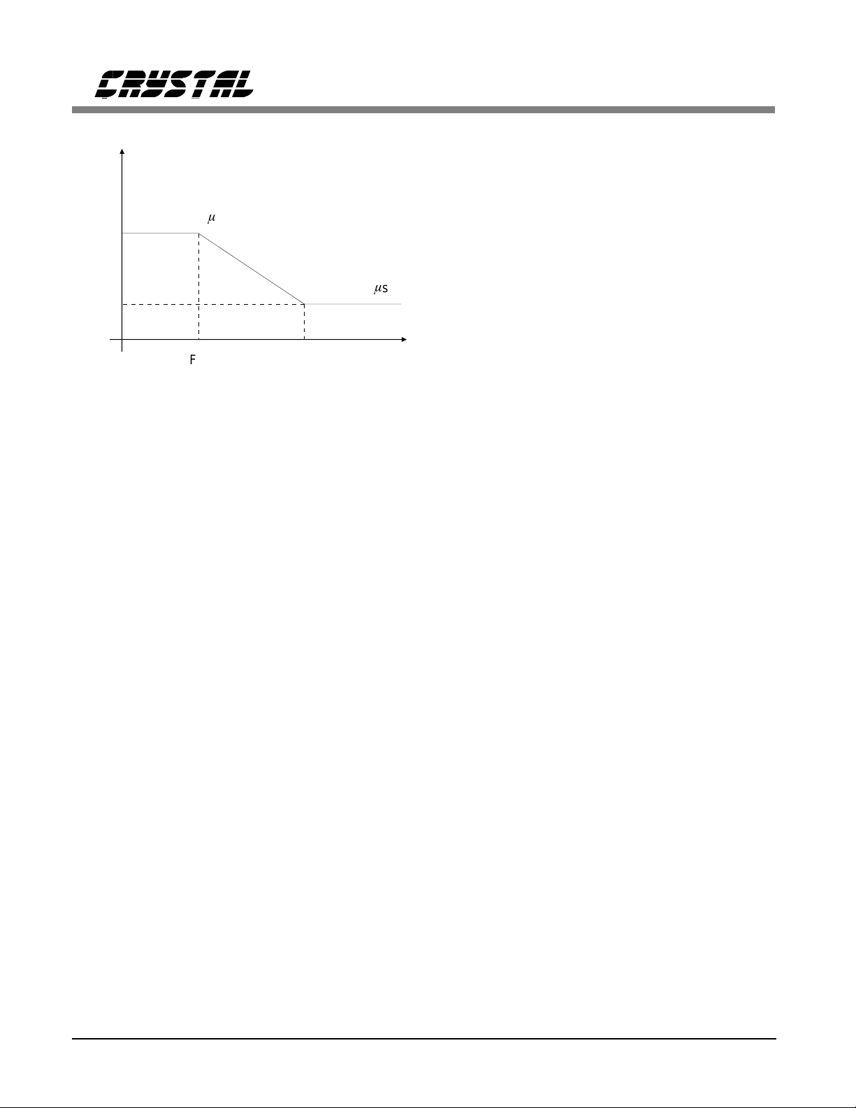
Gain
dB
0dB
T1=50
CS4330, CS4331, CS4333
CS4330/31/3 3 adapt to these new operating conditions. It is recomended that the CS4330/31/33
not be powered up with the clocks (MCLK,
LRCK, SCLK) going.
m
s
Power Supply Determination
m
T2 = 15
-10dB
F1 F2
3.183 kHz 10.61 kHz
Figure 3. De-Emphas is Curve (Fs = 44.1kHz)
s
Frequency
Initializatio n and Power-Down
The Initialization and Power-Down sequence
flow chart is shown in Figure 8. The CS4330/31/33
enter the Power-Down mode upon initial powerup. The interpolation filters and delta-sigma
modulators are reset, and the interna l voltage reference, one-bit digital-to-analog converters and
switched-capacitor low-pass filters are powered
down. The device will remain in the PowerDown mode until MCLK and LRCK are
presented. Once MCLK and LRCK are detect ed,
MCLK occurrence s are counted over one LRCK
period to determine the MCL K/LRCK frequency
ratio. Power is then applied to the internal voltage reference and the +5 or +3 Volt power
supply mode is determined. Finally, power is
applied to the D/A converters and switched-capacitor filters, and the analog outputs will move
to approximately 2.3V (1.3V in 3V mode). This
process requires approximately 1ms plus 1024
cycl es of LRC K.
The nominal power supply voltage for the
CS4330/31/33 may be either +5 or +3 Volts.
"SMART Analog" circuitry senses the power
supply voltage during the initialization sequence
or when exiting th e Power-Down mode. +5V operation will be set with a 3.7 Vpp full scale
output if VA+ is b etween 4.75 and 5.5 Volts. The
CS4330/31/3 3 will b e set for +3V o peration wi th
a 1.85 Vpp full scale output if VA+ is between
2.7 and 4.0 Volts. Supply voltages between 4.0
and 4.75 Volts should be avoided to prevent operation in the 5V mode. In this conditio n there is
insufficient headroom to pr oduce a 3.7 Vpp output.
Grounding and Power Supply Decoupling
As with any high resolution converter, the
CS4330/31/33 require careful attention to power
supply and grounding arrangements to optimize
performance. Figure 1 shows the recommended
power arrangements with VA+ connected to a
clean +3/+5V supply. Decoupling capacitors
should be located as near to the CS4330/31/33
as possible.
Analog Output and Filtering
The CS4330/3 1/33 analog filter is a switched -capacitor filter. The switched-capacitor filter
frequency response is clock dependent and will
scale with sample rate.
The CS4330/31/33 enter the Power-Down mode
within 1 period of LRCK if either MCLK or
LRCK is removed. The initialization sequence
begins when MCLK and LRCK are restored. If
the MCLK/LRCK frequency ratio or the VA+
voltage changes during Power-Down, the
DS136F1 9
The digital filter of the CS4330/31/33 is designed to compensate for the magnitude and
phase resp onse of a single-pole low-pass filter at
twice the sample rate . Output filters consisting of
a 2.4 kohm resistor and capacitor are recom-
CS4330, CS4331, CS4333
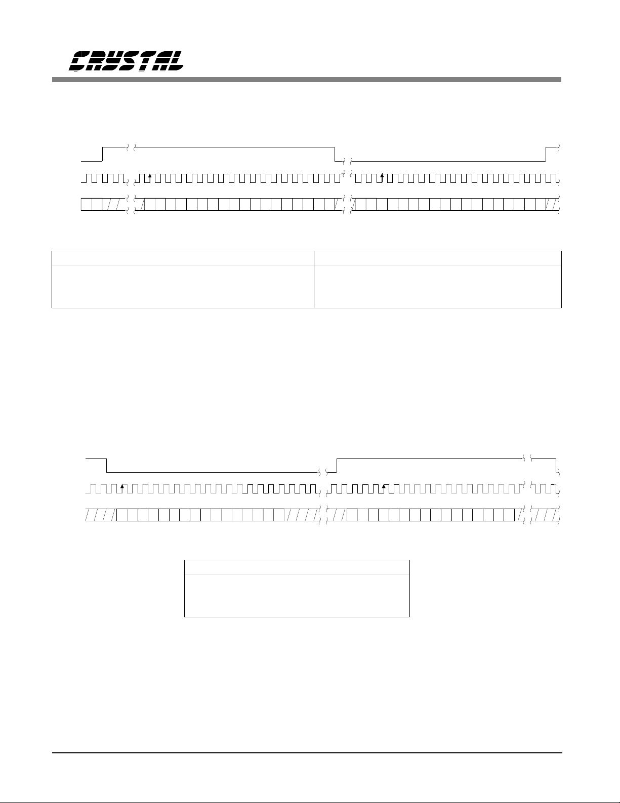
LRCK
SCLK
SDATA
10
17 16 17 16
Left Channel
15 14 13 12 11 10
Inter nal SCLK Mode
Right Justified, 18-Bit Data
Data Valid on Rising Edge of SCLK
INT SCLK = 64 Fs if MCLK/LRCK = 256 or 512
INT SCLK = 48 Fs if MCLK/LRCK = 3 84
6543210987
External SCLK Mode
Right Justified, 18-Bit Data
Data Valid on Rising Edge of SCLK
SCLK must have at least 36 cycles per LRCK
Figure 4. CS4330 Data Format
Right Chan nel
15 14 13 12 11 10
6543210987
LRCK
SCLK
SDATA 6543210987
15 14 13 12 11 10
Left Channel
Inter nal SCLK Mode
I2S, 16-Bit Data
Data Valid on Rising Edge of SCLK
INT SCLK = 32 Fs if MCLK/LRCK = 512 or 256
INT SCLK = 48 Fs if MCLK/LRCK = 3 84
Figure 5. CS4331 Internal SCLK Data Format (I2S)
15 14 13 12 11 10
Right Channel
6543210987
10 DS136F1
CS4330, CS4331, CS4333
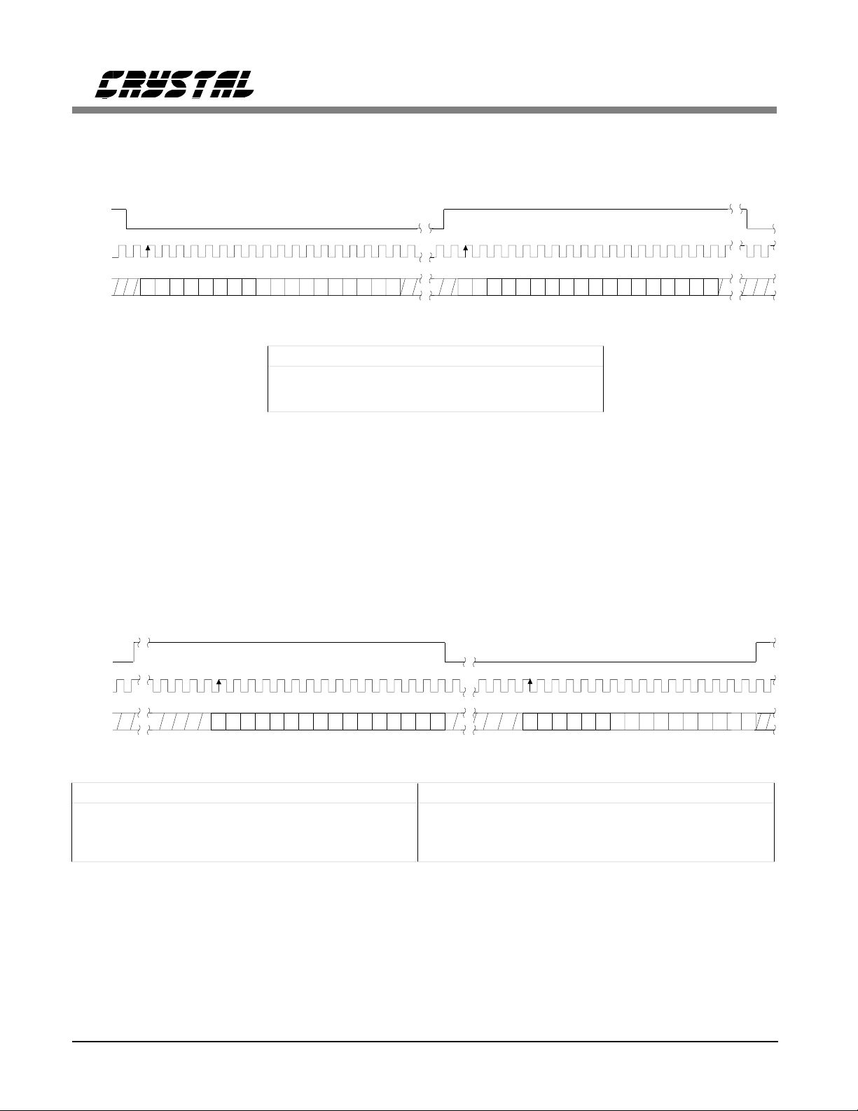
LRCK
SCLK
SDATA
Left Channel
654321098715 14 13 12 11 1017 16 654321098715 14 13 12 11 1017 16
External SCLK Mode
I2S, 18-Bit Data
Data Valid on Rising Edge of SCLK
SCLK must have at least 36 cycles per LRCK
Figure 6. CS4331 External SCLK Data Format (I2S)
Right Channel
LRCK
SCLK
SDATA
Left Channel
15 14 13 12 11 10
Inter nal SCLK Mode
Right Justified, 16-Bit Data
Data Valid on Rising Edge of SCLK
INT SCLK = 32 Fs if MCLK/LRCK = 512 or 256
6543210987
15 14 13 12 11 10
External SCLK Mode
Right Justified, 16-Bit Data
Data Valid on Rising Edge of SCLK
SCLK must have at least 32 cycles per LRCK
Right Channel
6543210987
INT SCLK = 48 Fs if MCLK/LRCK = 3 84
Figure 7. CS4333 SCLK Data Format
DS136F1 11
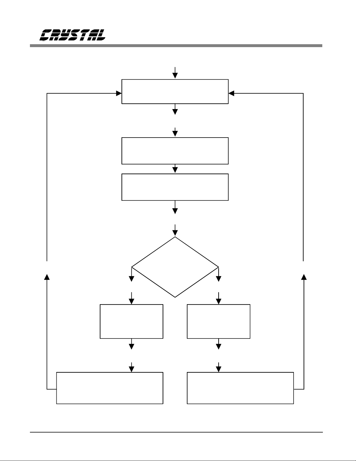
USER: Apply Power
Power-Down Mode
USER: Apply MCLK and LRCK
256/384/512
MCLK/LRCK Determination
Power Supply Determination
+3 or +5 Volt mode
CS4330, CS4331, CS4333
USER: set SCLK mode
Normal Operation
De-emphasis
available
USER: Apply SDATA
Analog Output
is Generated
SCLK mode
Normal Operation
USER: Apply SDATA
USER: Remove ClocksUSER: Remove Clocks
externalinternal
De-emphasis
not available
Analog Output
is Generated
Figure 8. CS4330/31/33 Initialization and Power-Down Sequence
12 DS136F1

CS4330, CS4331, CS4333
mended on the analog outputs. The required capacitor value is defined by:
C =
1
(2π) (Fs) (2400 Ω) (2)
Example: Fs = 48 kHz
C = 690 pF
A value of 680 pF may be used wi th only 1.45%
error which is negligib le.
Combined Digi tal and A nalog Filter Resp onse
The frequen cy response of the combined analog
switched-capacitor filter, digital filter, and offchip single pole RC-filter at 2 Fs, is shown in
Figures 9, 10, 11, and 12. The overall response
is clock dependent and will scale with Fs. Note
that the response plots have been normalized to
Fs and can be de-normalized by multiplying the
X-axis scale by Fs.
Figure 9. CS4330/31/33 Combined Digital and Analog
Filter Stopband Rejection
Figure 10. CS4330/31/33 Combined Digital and Analog
Filter Transition Band
DS136F1 13
Figure 11. CS4330/31/33 Combined Digital and Analog
Filter Transition Band
Figure 12. CS4330/31/33 Combined Digital and Analog
Filter Passband Ripple

Perf o r m an ce Pl ots
The following CS4330/31/33 measurement plots
were taken on the CDB4330/31/33 evaluation
board with an Audio Precision Dual Domain
System One. All plots are done i n +5V mode at
a 48 kHz sampling rate, and are shown in Figures 13-20.
Figure 13 shows the CS4330/3 1/33 frequency response. The response is flat to 20 kHz ± 0.1dB
as specified.
Figure 14 shows THD+N versus signal amplitude for a 1 kHz 20 -bit dithered in put signal.
Figure 15 shows a 16k FFT o f a 1 kHz full-scale
input signal. The signal has been filtered by a
notch filter within the System One to remove the
fundamental component of t he signal. Thi s minimizes the distortion created in the analyzer
analog-to-dig ital converter. This techn ique is discussed by Audio Precision in the 10th
anniversary edition of AUDIO.TST.
CS4330, CS4331, CS4333
Figure 13. Frequency Response
Figure 16 shows a 1 6k FFT of a 1 kHz -3 dBFs
input signal. The signal has been filtered by a
notch filter within the System One to remove the
fundamental componen t of the sig nal.
Figure 17 shows a 1 6k FFT of a 1 kHz -20 dBFs
input signal. The signal has been filtered by a
notch filter within the System One to remove the
fundamental componen t of the sig nal.
Figure 18 shows a 1 6k FFT of a 1 kHz -60 dBFs
input signal.
Figure 19 shows a 1 6k FFT of a 1 kHz -90 dBFs
input signal.
Figure 20 shows the fade-to-noise linearity. The
input signal is a dithered 18-bit 500 Hz sine
Figure 14. THD+N vs. Amplitude
Figure 15. 0 dBFs FFT
14 DS136F1

wave which fades from -60 to -120 dBFs. During the fade, the output from the CS4330/31/33
is measured and compared to the ideal level. Notice the very close tracking of the output level to
the ideal, even at l ow level inputs. This indica tes
very good low-level linearity, one of the key
benefits of delta-sigma digital-to-analog conversion.
CS4330, CS4331, CS4333
Figure 18. -60 dBFs FFT
Figure 16. -3 dBFs FFT
Figure 17. -20 dBFs FFT
DS136F1 15
Figure 19. -90 dBFs FFT
Figure 20. Fade-to-Noise Linearity

CS4330, CS4331, CS4333
Configuration Register
The CS4330, CS4331, CS4333 support multiple
2’s-complement data/clock formats. The require d
format is governed by the contents of the Configuration Register. The 5-bit register determines
which serial data format is acceptable, the frequency of the Internal Serial Clock, on which
edge of SCLK aud io data must be valid, and th e
number of bits to be loa ded into the input buffer.
On initial power-up, the register is loaded with
the default settings, and it is not necessary to
write to the register if this format is appropriate.
The default settings are shown in Figures 4-7.
The 8-bit code includes a 3-bit preamble to prevent accidental access to the Configuration
Register. Each bit of the cod e is read on the falling edge of LRCK as shown in the Figures 21
and 22. The code 01000000 is considered to be
an error condition and is ignored. The configuration routine requires that the SDATA pin is held
high, as shown in Figures 21 and 22, to prevent
accidental writ ing to the register. The Configuration Register is only accessible prior to entering
the External Serial Clock Mode. For I
2
S mode,
the user must set B6 to 0, and B7 to 1.
B1 B2 B3 B4 B5 B6 B7 B8
B1 B2 B3 Configuration Access Code
0 1 0 Access All owed
All other Codes Access Denied
B4 B5 Internal SCLK Mode only
Sets Internal SCLK/LRCK Ratio *
0 0 SCLK/LRCK = 32
01 Reserved
1 0 SCLK/LRCK = 64
1 1 SCLK/LRCK = 128
* The Internal SCLK wil l be 48 Fs, if the
MCLK/LRCK ratio is 384×.
B4 B5 External SCLK Mode only
Selects Data Sampling edge of SCLK
1 0 Rising edge of SCLK
1 1 Falling edge of SCLK
B6 Left or Right Justified Data
in relation to LRC K transition
0 Left Justified
1 Right Justified
B7 I
2
S Data Format
0Disabled
1Enabled
B8 Sets the number of Bits
0 18 Bits
Schematic & Layout Review Service
Confirm Optimum
Confirm Optimum
Schematic & Layout
Schematic & Layout
Before Building Your Board.
Before Building Your Board.
For Our Free Review Service
For Our Free Review Service
Call Applications Engineering.
Call Applications Engineering.
Call:(512)445-7222
16 DS136F1
1 16 Bits

Figure 21. Configuration Operation
CS4330, CS4331, CS4333
Figure 22. Configuration Timing
Parameter Symbol Min Typ Max Units
DEM/SCLK TIMING
DEM/SCLK valid to LRCK falling setup time t
LRCK falling to
DEM/SCLK hold time t
SDATA setup time t
SDATA hold time t
clrs
clrh
setup
hold
20 - - ns
20 - - ns
1--us
1--us
Table 2 . C onf ig urat io n T imin g C har acte rist ic s
DS136F1 17

REFERENCES
1)"An 18-Bit, 8-Pin Stereo Digital-to-Analog
Converter" by J.J. Paulos, A.W. Krone, G.D
Kamath, and S. T. Dupui e. Paper presented at the
97th Convention of the Au dio Engineering Society, November 1994.
2)"How to Achieve Optimum Performance from
Delta-Sigma A/D & D/A Converters" by Steven
Harris. Paper presented at the 93rd Convention
of the Audio Engineering Soci ety, October 1992.
3)"Multiplier-Free Interpolation for Oversampled
Digital-to-Analog Conversion" by Jeffrey W.
Scott. Paper presented at the 92nd Convention of
the Audio Engi neering Society, March 1992.
4)"An 18-Bit Stereo D/A Converter With Integrated Digital and Analog Filters" by Nav S.
Sooch, Jeffrey W. Scott. Paper presented at the
91st Convention of the Audio Engineering Society, November 1991.
CS4330, CS4331, CS4333
5)CDB4330/31/33 Evaluation board Data Sheet;
DS136DB2 MAR’96
18 DS136F1

PIN DESCRIPTIONS
CS4330, CS4331, CS4333
SERIAL DATA INPUT SDATA AOUTL ANALOG LEFT CHANNEL OUTPUT
DE-EMPHASIS / SCLK
LEFT / RIGHT CLOCK LRCK AGND ANAL OG GROUND
MASTER CLOCK MCLK AOUTR ANALOG RIGHT CHANNEL OUTPUT
DEM/SCLK VA+ ANALOG POWER
81
72
63
54
Power Supply Connections
VA+ - Positive Analog Power, PIN 7.
Positive analog supply. Nominally +5V or +3V.
AGND - Analog Ground, PIN 6.
Analog ground referen ce.
Analog Outputs
AOUTL - Analog Left Channel Output, PIN 8.
Analog outp ut for the left c hannel. Typically 3.7 Vpp for a full-scale input signal at VA+ = 5V
and 1.85 Vpp at VA+ = 3V.
AOUTR - Analog Right Channel Output, PIN 5.
Analog outpu t for the right channel. Typically 3.7 Vpp for a full-scale i nput signal a t VA+ = 5V
and 1.85 Vpp at VA+ = 3V.
Digital Inputs
MCLK - Master Clock Input, PIN 4.
The frequency must be 2 56×, 384× , or 512× th e input sample ra te (Fs).
LRCK - Left/Right Clock, PIN 3.
This input determines which channel is currently being input on the Audio Serial Data Input
pin, SDATA.
SDATA - Audio Serial Data Input, PIN 1.
Two’s complement MSB-first serial data is input on this pin. The data is clocked into the
CS4330, CS4 331, and CS433 3 via internal or extern al SCLK and the cha nnel is determined b y
LRCK.
DEM/SCLK - De-emphasis / External serial clock input , PIN 2.
A dual-purpose input u sed for de-emphasis filter control or external serial clock input .
DS136F1 19

CS4330, CS4331, CS4333
PARAMETER DEFINITIONS
Total Harmonic Distortion + Noise (THD+N)- The ratio of the rms value of the signal to the rms
sum of all other spectral components over the specified bandwidth (typic ally 10 Hz to 20 kHz),
including di stortion compon ents. Expressed in decibels.
Dynamic Range - The ratio of the full scale rms value of the signal to the rms sum of all other
spectral components over the specified bandwidth. Dynamic range is a signal-to-noise
measurement over the spe cified bandwidth mad e with a -60 d BFs signal. 60 dB is then added to
the resulting measurement to refer the measurement to full scale. This technique ensures that
the distortion components are below the noise level and do not effect the measurement. This
measurement techni que has been a ccepted by the Audio Engineering Society, AES17-1991, and
the Electroni c Indu stries Asso ciation of Japan, EIAJ CP-3 07.
Interchannel Isolation - A measure of crosstalk between the left and right channels. Measured for
each channel at the converter’s output with all zeros to the input under test and a full-scale
signal applied to the other cha nnel. Units i n decibels.
Interchannel Gain Mismatch - The gain difference between left a nd right channel s. Units in deci bels.
Gain Error - The deviation from the n ominal ful l scale analo g output f or a full scale dig ital input.
Gain Drift - The chan ge in gain value wit h temperatu re. Units in pp m/°C.
20 DS136F1

ORDERING INFORMATION:
Model Temperature Package
CS4330-KS -1 0 to +70°C 8 -pin Plasti c SOIC
CS4331-KS -1 0 to +70°C 8-pin Plastic SOIC
CS4333-KS -1 0 to +70°C 8-pin Plastic SOIC
CS4330-BS -40 to +85 °C 8-pin Plasti c SOIC
CS4331-BS -40 to +85 °C 8-pin Plasti c SOIC
CS4333-BS -40 to +85 °C 8-pin Plasti c SOIC
PACKAGE DIMENSIONS
CS4330, CS4331, CS4333
A
8-Pin
SOIC
B
E
F
C
D
H
J
G
I
Note: The EIAJ package is n ot a standa rd JEDEC packag e size
A
B
C
D
E
F
G
H
I
J
MILLIMETERS
MIN MAX
5.15 5.35
1.27
0
1.77 1.88
0.33 0.51
0.15 0.25
5.18
0.48 0.76
7.67
TYP
0.25
5.4
8.1
INCHES
MAXMINDIM
0.203 0.210
0.050 TYP
0
0.070 0.074
0.013
0.006 0.010
080
0.204
0.010
0.020
8
0.213
0.0300.019
0.3190.302
DS136F1 21

• Notes •

CDB4330
CDB4331 CDB4333
Evaluation Board for CS4330 / CS4331 / CS4333
Features
Demonstrates recommended layout
•
and grounding arrangements
CS8412 Receives AES/EBU, S/PDIF,
•
& EIAJ-340 Compatible Digital Audio
Digital and Analog Patch Areas
•
Requires only a digital signal source
•
and power supplies for a complete
Digital-to-Analog-Converter system
General Description
The CDB4330/31/33 evaluation board is an excellent
means for quickly evaluating the CS4330/31/33 18-bit,
stereo D/A converter. Evaluation requires an analog
signal analyzer, a digital signal source and a power
supply. Analog outputs are provided via RCA connectors for both channels.
The CS8412 digital audio receiver I.C. provides the
system timing necessary to operate the CS4330/31/33
and will accept AES/EBU, S/PDIF, and EIAJ-340
compatible audio data. The evaluation board may also
be configured to accept external timing signals for operation in a user application during system
development.
ORDERING INFORMATION: CDB4330, CDB4331,
CDB4333
Digital
Audio
Input
CS8412
Digital
Audio
Interface
Crystal Semiconductor Corporation
P.O. Box 17847, Austin, TX 78760
(512) 445-7222 Fax: (512) 445 7581
I/O for
Clocks
and Data
CS4330/31/33
Copyri ght Crystal Semiconductor Corporation 1996
(All Rights Reserved)
Analog
Filter
MAR ’96
DS136DB2
23

CDB4330, CDB4331, CDB4333
CDB4330/31/3 3 System Overview
The CDB4330/31/33 evaluation board is an excellent means of quickly evaluating the
CS4330/31/33. The CS8412 digital audio interface receiver provides an eas y interface to digita l
audio signal sources including the majority of
digital audio test equipment. The evaluation
board also allows the user to supply clocks and
data through a 10-pin he ader for system development.
The CDB4330/31/33 schematic has been partitioned into 5 schematics shown in Figures 2
through 7. Each partitioned schematic is represented in the system diagram shown in Figure 1.
Notice that the the sy stem diagram al so includes
the interconnections between the partitioned
schematics.
CS4330/31/33 Digital t o Analo g Converter
A description of the CS43 30/31/33 is include d in
the CS4330/31 /33 data shee t.
CS8412 Digital Audio Receiver
When the Error Information Switch is activated,
the CS8412 op erates in the Error and Freq uency
information mode . The information display ed by
the LED’s can be decoded by consulting the
CS8412 data sheet. If the Error Information
Switch is activated, and the CS4330/31/33 is in
the internal serial clock mode, then it is likely
that the de-emphasis control for the
CS4330/31/33 will be erroneous and produce an
incorrect audio outp ut.
Encoded sample frequency information can be
displayed provided a proper clock is being applied to the FCK pin of the CS8412. When an
LED is lit, this indicates a "1" on the corresponding pin located on the CS8412. When an
LED is off, this indicates a "0" on the corresponding pin. Neither the L or R option of
CSLR/FCK sh ould be selected if the FCK pin is
being driven by a clock si gnal.
The evaluation board has been designed such
that the input can be either optical or coax, Figure 6. It is not necessary to select the active
input. However, both inputs can not be driven simultaneou sly.
The system receives and decodes the standard
CS8412 Data Format
S/PDIF data format using a CS8412 Digital
Audio Receiver, Figure 4. The outputs of the
CS8412 include a serial bit clock, serial data,
left-right clock (FSYNC), de-emphasis control
and a 256Fs master clock. The operation of the
CS8412 and a discussi on of the digital audio interface are included in the 1994 Crystal
Semiconducto r Audio Data Book.
The CS8412 data format c an be set with jumpers
M0, M1, M2, and M3. These form ats are shown
in the CS84 12 datasheet fo und in the 1994 Crys-
tal Semicondu ctor Audio Data Book. The format
selected must be compatible with the corresponding data format of the CS4330/31/33
shown in Figures 4-7 of the CS4330/31/33
datasheet. The default settings for M0-M3 on the
During normal operati on, the CS8412 operates in
the Channel Status mode where the LED’s display channel status information for the channel
evaluation board are given in Tables 2-4. The
compatible data formats we have chosen for the
CS8412 and CS4 330/31/33 are:
selected by the CSLR/FCK jumper. This allows
the CS8412 to deco de and supply the de-emphasis bit from the digital audio in terface for control
of the CS4330/31/33 de-emphasis filter via
pin 3, CC/F0, of t he CS8412.
24 DS136DB2
CS8412 format 6;CS 4330
CS8412 format 2;CS 4331 (External SCLK only)
CS8412 format 5;CS 4333 (External SCLK only)

CDB4330, CDB4331, CDB4333
Analog output fil ter
The recommended single pole filter required for
the CS4330/31/33 has been combined with a
unity gain output buffer (see Figure 2). The an alog output filter uses a Motorola MC33202
single supply, dual op-amp. The low pass filter
corner freq uency is located at 2 Fs , or 88.2 kHz
and is calcu lated by:
F
=
F
=
(2π) (
(2π) (15
1
R
||
R
) (
8
k
C
9
29
1
Ω || 6.65kΩ) (390
)
= 88.5 kHz
pF
)
Power Supply Circuitry
Power is supplied to the evaluation board by
three binding posts (GND, +5V, +3V/+5V), See
Figure 7. The +5V input supplies power to the
+5 Volt digital circuitry (VD+5), while the
+3V/+5V input supplies power to the Voltage
Level Converter (VD+3/+5), and CS4330/31/33
(VA+3/+5) for evaluation in either +3 o r +5 Volt
mode. The op-amp is supplied from the analog
supply (VA+) which can be derived from either
the +5V post (VA+5) or the +3/+5V post
(VA+3/+5) depending upon which Ferrite bead
(L4 or L5) is installed. The evaluation board is
configured with VA+ derived from VA+5 (L5 installed). To derive VA+ from the +3V/+5V post
(VA+3/+5), remove the Ferrite bead at L5, and
install it at L 4.
Input/Output for Clocks and Da ta
The evaluation board has been designed t o allow
the interface to external systems via the 10-pin
header, J1. This header allows the evaluation
board to accept externally generated clocks and
data. The schematic for the clock/data I/O is
shown in Figure 5. The 74HC243 transceiver
functions as an I/O buffer where the CLK
SOURCE jumper determines if the transceiver
operates as a transmitte r or receiver.
The transceiver operates as a transmitter with the
CLK SOURCE jumper in the 8412 position.
LRCK, SDATA, and SCLK from the CS8412
will be available on J1. J22 must be in th e 0 po-
sition and J23 must be in the 1 position for
MCLK to be an output and to avoid bus conten-
tion on MCLK.
The transceiver operates as a receiver with the
CLK SOURCE jumper in the EXTERNAL posi-
tion. LRCK, SDATA and SCLK on J1 become
inputs. The CS8412 must be removed from the
evaluation board for op eration in t his mode.
There are 2 options for the source of MCLK in
the External Clock Source mode. MCLK can be
an input wi th J23 in th e 1 position a nd J22 in the
0 position. However, the recommended mode of
operation is to generat e MCLK on the evaluation
board. MCLK becomes an output with LRCK,
SCLK and SDATA inputs. Thi s technique insures
that the CS43 30/31/33 receives a jitter free clock
to maximize performance. This can be accom-
plished by installing a crystal oscillator into U5,
see Figure 4 (the soc ket for U5 is located within
the footprint for th e CS8412) and placing J22 in
the 1 position and J23 in the 0 position.
Grounding and Power Supply Decoupling
The CS4330/31/33 requires careful attention to
power supply and grounding arrang ements to op-
timize performance. Figure 2 shows the
recommended power arrangements. The
CS4330/31/33 is positioned over the analog
ground plane near the digital/analog ground
plane split. These ground planes are connected
elsewhere on the board. This layout techni que is
used to minimizing digital noise and to insure
proper power supply matching/sequencing. The
decoupling capacitors are locate d as close to the
CS4330/31/33 as possible. Extensive use of
ground plane fill on both the analog and digital
sections of the evaluation board yield large re-
ductions in radiated noise effects.
DS136DB2 25

CDB4330, CDB4331, CDB4333
CONNECTOR INPUT/OUTPUT SIGNAL PRESENT
input (VD+5V) for CS8412 and digital section
+5V
+3/+5V
input
input (VD+3/+5V) for Voltage Level Converter
(VA+) for Analog output filter op-amp
(configured for +5V)
input (VA+3/+5V) for CS4330/31/33
GND input ground connection from power supply
Digital Input input digital audio interface input via coax
Optical Input input digital audio interface input via optical
MCLK, SCLK,
LRCK
input/output I/O for master, serial, and left/r ight clocks
SDATA input/output I/O for serial data
AOUTL output left channel analog output
AOUTR output right channel analog output
Table 1. System Connections
JUMPER PURPOSE POSI TION FUNCT ION SELECTED
selects channel for
CSLR/FCK
CS8412 channel status
informat ion
Clock
Select
J22
J23
Selects source of
system clocks and data
Selects MCLK as Input
or Output
M0
M1 *High
CS8412 mode select
M2 *High
L
See CS8412 data sheet for details
R
*8412 CS8412 clock/data source
EXT External clock/data source
*0
*1
Input/Output for Clocks and
See
Data
section of text
*Low
See CS8412 data sheet
for details
M3 *Low
SCLK Selects SCLK Mode
INT Internal SCLK Mode
*EXT Exter nal SCLK Mode
DEM_8412
* Default set ti ng f rom fa ctor y
Selects source of de-
emphasis control
*Low CS8412 de-emphasis
High De-emphasis input static high
Table 2. CDB4330 Ju mper Sel ectabl e Option s
26 DS136DB2

CDB4330, CDB4331, CDB4333
JUMPER PURPOSE POSI TION FUNCT ION SELECTED
CSLR/FCK
selects channel for
CS8412 channel status
informat ion
L
See CS8412 data sheet for details
R
Clock
Select
J22
J23
M0
M1 *High
M2 *Low
Selects source of
system clocks and data
Selects MCLK as Input
or Output
CS8412 mode select
*8412 CS8412 clock/data source
EXT External clock/data source
*0
*1
Input/Output for Clocks and
See
Data
section of text
*Low
See CS8412 data sheet
for details
M3 *Low
SCLK Selects SCLK Mode
INT Internal SCLK Mode (Note 1)
*EXT Exter nal SCLK Mode (Note 1)
DEM_8412
* Default set ti ng f rom fa ctor y
Note 1. The CS8412 output data format requires the CS4331 be in the External SCLK Mode
Selects source of de-
emphasis control
Table 3. CDB4331 Ju mper Sel ectabl e Option s
*Low CS8412 de-emphasis
High De-emphasis input static high
JUMPER P URPOSE POSITION F UNCTION SELECTED
CSLR/FCK
selects channel for
CS8412 channel status
information
L
See CS8412 data sheet for details
R
Clock
Select
J22
J23
M0
M1 *Low
M2 *High
Selects source of
system clocks and data
Selects MCLK as Input
or Output
CS8412 mode select
*8412 CS8412 clock/data source
EXT E xternal clock/data source
*0
*1
Input/Output for Clocks and
See
Data
section of text
*High
See CS8412 data sheet
for details
M3 *Low
SCLK Selects SCLK Mode
INT Internal SCLK Mode (Note 1)
*EXT Exter nal SCLK Mode (Note 1)
DEM_8412
* Default setting from factory
Note 1. The CS8412 output data format requires the CS4333 be in the External SCLK Mode
DS136DB2 27
Selects source of de-
emphasis control
Table 4. CDB4333 Jumper Selectable Options
*Low CS8412 de-emphasis
High De-emphasis input static high

CDB4330, CDB4331, CDB4333
Digital
Audio
Input
Fig 6
RXP
RXN
CS8412
Digital
Audio
Interface
MCLK
LRCK
SCLK
SDATA
I/O for
Clocks
and Data
Fig 5
Power
Down
Voltage
Level
Converter
MCLK
LRCK
SCLK
SDATA
CS4330/31/33
Fig 2
AOUTL
Analog
Filter
AOUTR
Fig 2
Fig 3
Fig 3
Fig 4
Figure 1. System Block Diagram and Signal Flow
28 DS136DB2

DS136DB2 29
Figure 2. CS4330/31/33 and Connections
CDB4330, CDB4331, CDB4333

CDB4330, CDB4331, CDB4333
Figure 3. Voltage Level Conversio n and Power Down Circuitry
30 DS136DB2

DS136DB2 31
NOTE: U2 and U5 cannot be installed simulta neously
Figure 4. CS8412 Digital Audio Receiver Connections
CDB4330, CDB4331, CDB4333

Figure 5. I/O I nterf ace f or C locks and Data
CDB4330, CDB4331, CDB4333
Figure 6. Digital Audio Input
Optical Toshiba part TORX173 available through Insight Electronics
32 DS136DB2

CDB4330, CDB4331, CDB4333
Figure 7. Power Supply
DS136DB2 33

CDB4330, CDB4331, CDB4333
Figure 8. CDB4330/31/33 Component Side Silkscreen
34 DS136DB2

CDB4330, CDB4331, CDB4333
Figure 9. CDB4330/31/33 Component Side (top)
DS136DB2 35

CDB4330, CDB4331, CDB4333
Figure 10. CDB4330/31/33 Solder Side (bottom)
36 DS136DB2

• Notes •

Advance product information describes products which are in development and subject to development changes. Cirrus Logic, Inc. has made
best efforts to ensure that the information contained in this document is accurate and reliable. However, the information is subject to change
without notice and is provided “AS IS” without warranty of any kind (express or implied). No responsibility is assumed by Cirrus Logic, Inc. for
the use o f this in forma tio n, nor for infri nge men ts of p aten ts or other rights of third p artie s. This docum ent i s the p roper ty of Cirr us Logic , Inc. and
implies no license under patents, copyrights, trademarks, or trade secrets. No part of this publication may be copied, reproduced, stored in a
retrieval system, or transmitted, in any form or by any means (electronic, mechanical, photographic, or otherwise). Furthermore, no part of this
publication may be used as a basis for manufacture or sale of any items without the prior written consent of Cirrus Logic, Inc. The names of
products of Cirrus Lo gi c, Inc . or other vendors an d supp li ers app eari ng i n t his d oc ume nt m ay be trademarks or s erv ice m ark s o f their respective
owners which may be registered in some jurisdictions. A list of Cirrus Logic, Inc. trademarks and service marks can be found at http://www.cirrus.com.
 Loading...