

Page 1
p
m
CS22220 Data Sheet
Wireless PCMCIA Controller
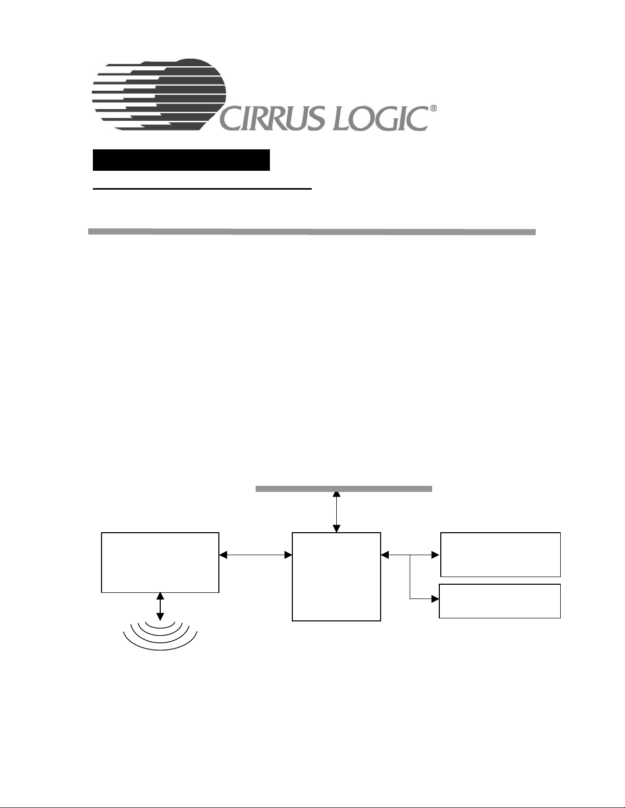
1 Description
The Cirrus Logic CS22220 Wireless Network Controller enables high performance, 11 Megabits per
second digital wireless data connectivity for PCMCIA, mobile, embedded systems and other cost
sensitive applications.
The CS22220 is a highly integrated single-chip PCMCIA solution for wireless networks supporting
video, audio, voice, and data traffic. The programmable controller executes Cirrus Logic’s
Whitecap™2 networking protocol that provides Wi-Fi™ (802.11b) compliance as well as multimedia
and quality of service (QoS) support. The device includes several high performance components
including an ARM7TDMI RISC processor core, a Forward Error Correction (FEC) codec and a
wireless radio MAC supporting up to11 Mbps throughput. The CS22220 utilizes state of the art
0.18um CMOS process and is housed in a 208 FPBGA compact (15mm x 15mm) package, which
has low-lead inductance suitable for highly integrated radio applications. The core is powered at 1.8
V with 3.3V (5.0V tolerant) I/O to reduce overall power consumption. In addition, the CS22220
supports low power management for the host and radio interfaces.
The CS22220 is designed to be an integral part of a PC card (PCMCIA 2.1/JEIDA 4.2). The
PCMCIA host interface also supports both little endian and big endian protocol for easy interfacing
to popular microprocessors in embedded system applications.
PCMCIA Host or Embedded CPU
Networking Data
802.11b compatible
2.4 GHz
Digital Radio
PHY Transceiver
2.4 GHz Direct Sequence
S
read Spectru
CS22220 Wireless PCMCIA Controller 1 of 34 DS557PP2 Rev. 3.0
11 Mbps
Wireless
Baseband I/F
Figure 1. Example System Block Diagram
www.cirrus.com
CS22220
Wireless
PCMCIA
Controller
System Memory
SDRAM (Up to 4MB)
SRAM (Up to 256KB)
Boot ROM/Flash
(Upto1MB)
Page 2

2 Features
Embedded ARM Core and System Support Logic
• High performance ARM7TDMI RISC processor core up to 77MHz
• 4KB integrated, one-way set associative, unified, write through cache
• Individual interrupt for each functional block
• Two 23-bit programmable (periodic or one-shot) general purpose timers
• 8 Dword (32-bits) memory write and read buffers for high system performance
• Abort cycle detection and reporting for debugging
• ARM performance monitoring function for system fine-tuning
• Programmable performance improvement logic based on system configuration
Enhanced Memory Controller Unit
• Programmable memory controller unit supporting SDRAM /async SRAM/Boot ROM/Flash
interface
• 16-bit data bus with 12-bit address supporting up to 4MB up to 103 MHz (100/133MHz SDRAM)
• 8-bit data bus with addressing support up to 1MB of boot ROM/Flash.
• Programmable SDRAM timing and size parameters such as CAS latencies and number of
banks, columns, and rows
• Flexible independent DMA engines for PCMCIA and digital radio functional units
FEC codec
• High performance Reed-Solomon coding for error correction (255:239 block coding)
• Reduces error probability of a typical 10e-3 error rate environment to 10e-9
• Programmable rate FEC engine to optimize channel efficiency
• Low latency, fully pipelined hardware encoding and decoding. Supports byte-wise single cycle
throughput up to 77MHz, with a sustain rate of 77MBps.
• Double buffering (63 Dword read/write buffer) to enhance system performance
Digital Radio MAC Interface
• Glue-less interface to 802.11b baseband transceivers
• Up to 11Mbps data rates
• 32 Dword transmit/receive FIFO
• Supports clear channel assessment (CCA)
Power Management
• Host (PCMCIA) ACPI compliant
• Programmable sleep timer for ARM core and system low power management
• Independent power management control for individual functional units
• Supports variable rate radio transmit, receive, and standby radio power modes
Clock and PLL Interface
• Single 44MHz crystal oscillator reference clock
• Internal PLL to generate internal and on board clocks
PCMCIA Interface
• 16 bit PCMCIA I/O target device supporting memory map or program I/O using 11 address bits
• Independent DMA controller to transfer data between PCMCIA and main memory
• Fully compliant with PCMCIA 2.1/JEIDA 4.2 standard
• Supports big endian and little endian (default) data formats
• Supports custom mode for embedded applications where the interface becomes a generic
memory address/data interface
Chip Processing and Packaging
• 208 FPBGA package and 0.18um state of the art CMOS process
• 1.8 V core for low power consumption. 3.3V I/O - 5V tolerant I/O
CS22220 Wireless PCMCIA Controller 2 of 34 DS557PP2 Rev. 3.0
www.cirrus.com
Page 3

IMPORTANT NOTICE
"Preliminary" product information describes products that are in production, but for which full characterization data is not yet
available. "Advance" product information describes products that are in development and subject to development changes.
Cirrus Logic, Inc. and its subsidiaries ("Cirrus") believe that the information contained in this document is accurate and
reliable. However, the information is subject to change without notice and is provided "AS IS" without warranty of any kind
(express or implied). Customers are advised to obtain the latest version of relevant information to verify, before placing
orders, that information being relied on is current and complete. All products are sold subject to the terms and conditions of
sale supplied at the time of order acknowledgment, including those pertaining to warranty, patent infringement, and limitation
of liability. No responsibility is assumed by Cirrus for the use of this information, including use of this information as the
basis for manufacture or sale of any items, or for infringement of patents or other rights of third parties. This document is the
property of Cirrus and by furnishing this information, Cirrus grants no license, express or implied under any patents, mask
work rights, copyrights, trademarks, trade secrets or other intellectual property rights. Cirrus owns the copyrights of the
information contained herein and gives consent for copies to be made of the information only for use within your organization
with respect to Cirrus integrated circuits or other parts of Cirrus. This consent does not extend to other copying such as
copying for general distribution, advertising or promotional purposes, or for creating any work for resale.
An export permit needs to be obtained from the competent authorities of the Japanese Government if any of the products or
technologies described in this material and controlled under the "Foreign Exchange and Foreign Trade Law" is to be
exported or taken out of Japan. An export license and/or quota needs to be obtained from the competent authorities of the
Chinese Government if any of the products or technologies described in this material is subject to the PRC Foreign Trade
Law and is to be exported or taken out of the PRC.
CERTAIN APPLICATIONS USING SEMICONDUCTOR PRODUCTS MAY INVOLVE POTENTIAL RISKS OF DEATH,
PERSONAL INJURY, OR SEVERE PROPERTY OR ENVIRONMENTAL DAMAGE ("CRITICAL APPLICATIONS").
CIRRUS PRODUCTS ARE NOT DESIGNED, AUTHORIZED, OR WARRANTED TO BE SUITABLE FOR USE IN LIFESUPPORT DEVICES OR SYSTEMS OR OTHER CRITICAL APPLICATIONS. INCLUSION OF CIRRUS PRODUCTS IN
SUCH APPLICATIONS IS UNDERSTOOD TO BE FULLY AT THE CUSTOMER'S RISK.
Cirrus Logic, Cirrus, and the Cirrus Logic logo designs are trademarks of Cirrus Logic, Inc. All other brand and product
names in this document may be trademarks or service marks of their respective owners.
Use of this product in any manner that complies with the MPEG-2 video standard as defined in ISO
documents IS 13818-1 (including annexes C, D, F, J, and K), IS 13818-2 (including annexes A, B,
C, and D, but excluding scalable extensions), and IS 13818-4 (only as it is needed to clarify IS
13818-2) is expressly prohibited without a license under applicable patents in the MPEG-2 patent
portfolio, which license is available from MPEG LA, L.L.C. 250 Steele Street, Suite 300, Denver,
Colorado 80296.
CS22220 Wireless PCMCIA Controller 3 of 34 DS557PP2 Rev. 3.0
www.cirrus.com
Page 4
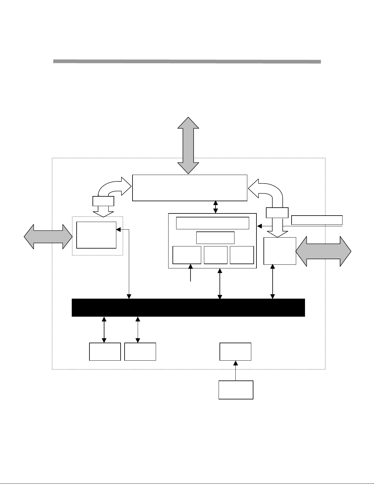
3 Functional Description
Figure 2. Block Diagram of Major Functional Units
System Memory
Memory/Boot ROM
Controller
Arbiter
DMA
PCMCIA
PCMCIA
Controller
w/DMA Ctrl
Sleep
Timer
FEC codec
Read/Write Buffer
ARM 7TDMI
Interrupt
controller
System Control Bus
Timer
(2)
4KB
Cache
Clock/PLL
Crystal or
Oscillator
DMA
Radio MAC
w/ DMA Ctrl
JTAG/Test Interface
Digital Radio
Interface
CS22220 Wireless PCMCIA Controller 4 of 34 DS557PP2 Rev. 3.0
www.cirrus.com
Page 5

3.1 Embedded ARM Core and System Support Logic
The processing elements of the CS22220 include the ARM7TDMI core and its associated
system control logic. The ARM processor and system controller consists of a memory
management unit, 4-KB write through cache controller, 20 IRQ and 4 FIRQ interrupt
controller, and 2 general purpose timers. The ARM processor and integrated system
support logic provide the necessary execution engine to support a real time multi-tasking
operating system, the network protocol stack, and firmware services.
Memory Management Unit
ARM instructions and data are fetched from system memory a cache-line (4/8 – Dwords
/Programmable) at a time when caching is turned on. During a cache line fill, critical word
data, i.e., the access that caused the miss, is forwarded to the ARM and also written into
the data RAM cache. The non-critical words in the line fetched following the critical word
are then written to the cache on a Dword basis, as they become available.
Memory writes are posted to dual 4-Dwords (32-bit) memory write posting buffers. Write
posts use the sequential addressing feature on the memory bus. With dual buffering an out
of sequence write will post to one write buffer while the other buffer is flushed to memory.
There is one 8Dword Read Buffer in the MEM block. The buffer is used for both cacheable
and non-cacheable memory space.
Interrupt Controller
The interrupt controller provides two interrupt channels to the ARM processor. One
interrupt channel is presented to the ARM on its nFIQ, and the other channel is presented
on its nIRQ pin. These are referred to as the FIQ channel and the IRQ channel. Both
channels operate in identical but independent fashion. The FIQ channel has a higher
priority on the ARM processor than the IRQ channel.
The interrupt controller includes a CONTROL register for each logical interrupt in the ARM
Complex. The CONTROL register serves the following main purposes:
• Provides the mapping between the EXT_INT inputs (physical interrupts) and the logical
interrupt
• Selects the particular type of signaling expected on the EXT_INT inputs: level, edge,
active level high/low etc.
• Enable or disable a logical interrupt
CS22220 Wireless PCMCIA Controller 5 of 34 DS557PP2 Rev. 3.0
www.cirrus.com
Page 6

3.2 Digital Radio Interface
The CS22220 digital radio MAC I/F supports multiple radio baseband and RF interfaces.
The baseband registers can be programmed during the configuration time using the control
port interface. The MAC also provides the capability of programming the signal, service and
length on per packet basis without ARM intervention. This significantly improves the
performance of the system.
There are three primary digital interface ports for the CS22220 that are used for
configuration and during normal operation.
These ports are:
• The Control Port, which is used to configure, set power consumption modes, write
and/or read the status of the radio base band registers.
• The TX Port, which is used to output the data that needs to be transmitted from the
network processor.
• The RX Port, which is used to input the received demodulated data to the network
processor
3.3 FEC Codec
The FEC codec performs Reed-Solomon coding to protect the data before it is transmitted
to a noisy channel. It is a similar code as employed by the digital broadcast industry, such
as ITU-T J.83 for DVB. The RS(255, 8) code implemented by the CS22220 can reduce
error probability to 1/10e-9 in a typical 1/10e-3 error rate environment. The
encoder/decoder can be programmed to vary the coding block length (N) and correctable
error (t) to optimize the tradeoff between channel utilization and data protection. The range
of N iscurrentlysettobefrom20to255,andthet is 8. The symbol size is fixed at 8 bits.
Coding parameters can be set real time, allowing maximum flexibility for the system to
adjust the FEC setting, such as block size, in order to optimize channel efficiency. The
encoder also has a very low latency of two cycles. Both the encoder and decoder are fully
pipelined in structure to achieve single cycle throughput. The FEC can be disabled in
firmware.
CS22220 Wireless PCMCIA Controller 6 of 34 DS557PP2 Rev. 3.0
www.cirrus.com
Page 7

3.4 Programmable Memory Controller
The CS22220 incorporates a general-purpose memory controller. The memory controller
supports both SDRAM/async SRAM memory interface and a FLASH memory interface.
In the RAM configuration, the system memory interface supports up to 4-Mbyte of 16-bit
SDRAM running at frequency up to 103 MHz (using 133MHz SDRAM) single-state access
cycles or 256KB of 16 bit async SRAM. The memory controller provides programming of
SDRAM parameters such as CAS latency, refresh rate and etc; these registers are located
in miscellaneous configuration registers. The CS22220 memory controller supports the
power saving feature of the SDRAM by toggling the clock enable (CKE) signal. When there
are no pending memory requests from any internal requester, the CS22220 will keep CKE
low to cause the SDRAM to stay in power down mode. Once a memory request is active,
the CS22220 will assert CKE high to cause the SDRAM to come out of power down mode.
Typically, this can reduce memory power consumption by up to 50%.
In ROM configuration, firmware for CS22220 is stored in non-volatile memory and is
accessed through the boot ROM interface. The maximum addressable ROM space
supported is 1MB. ROM read/write and output enable are shared with RAM control pins.
3.5 PCMCIA Interface
The PC-Card interface implemented in Cirrus Logic CS22220 is fully compliant with
PCMCIA 2.1/JEIDA 4.2. The interface supports 16 data bits PCMCIA program I/O and
memory mapped accesses using 11 address bits. PCMCIA interface allows laptop users to
connect to home network to access data and multimedia streams with ease. The interface
provides both memory and I/O access.
The PCMCIA interface incorporates an independent DMA controller to transfer data to/from
the main memory. The ARM has the flexibility in controlling how often it is interrupted and
simplifies the packet transmit/receive protocol. The DMA controller is programmed during
power up.
The CS22220 PCcard interface incorporates a custom mode, which can be used for
embedded applications, by bypassing the standard PC card Pnp configuration
requirements. This interface thus becomes a generic asynchronous 16 bit data interface.
This mode is useful when interfacing the CS22220 wireless network controller directly to an
embedded micro-controller capable of supporting a 16 bit data bus.
CS22220 Wireless PCMCIA Controller 7 of 34 DS557PP2 Rev. 3.0
www.cirrus.com
Page 8
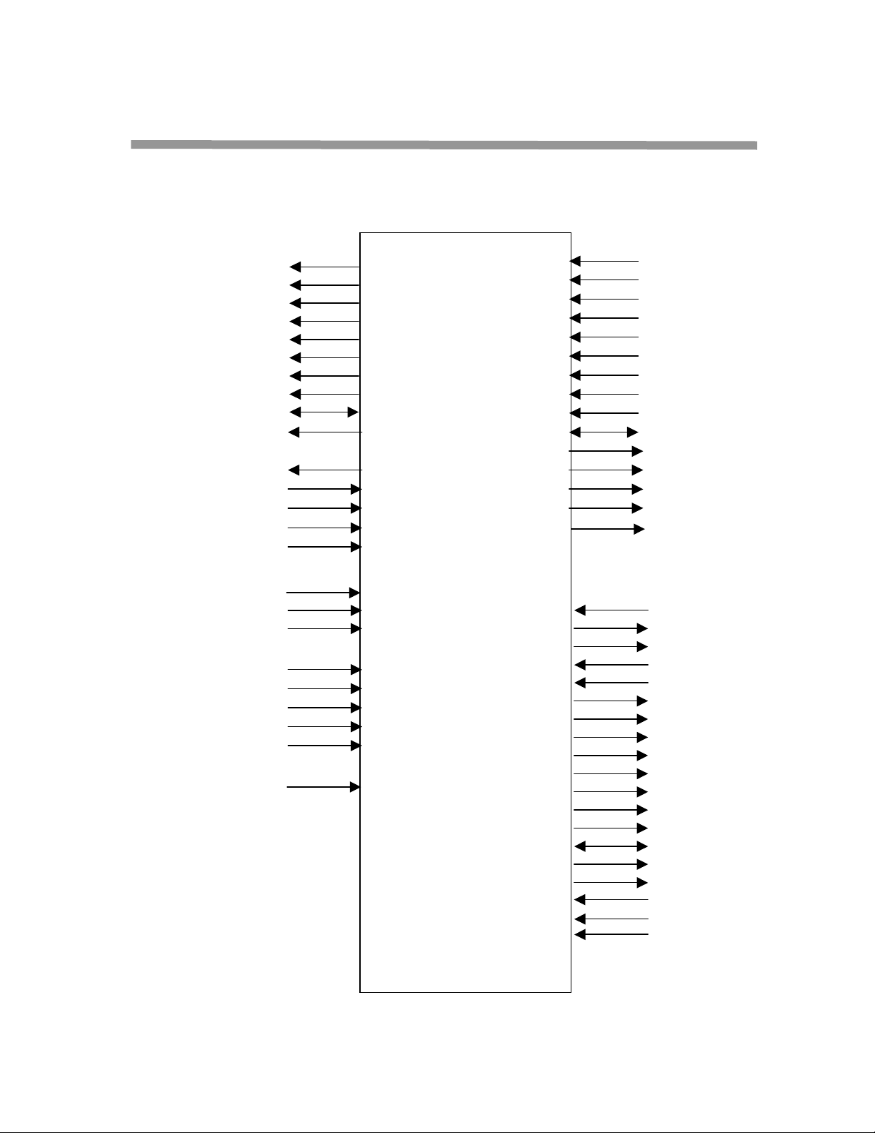
4 Pinout and Signal Descriptions
N
T
I
K
K
T
Figure 3. CS22220 Logical Pin Groupings
System
Memory
Interface
JTAG
Interface
Clock Interface
PLL Power
Interface
SMCLK
nSMCS[1:0]
nSMRAS
nSMCAS
nSMWE
SMDQM[1:0]
SMCKE
SMA[11:0]
SMD[15:0]
nBRCE
TDO
TD
TC
TMS
nTRST
XTRACL
XTALCLKI
XTALOU
PLLAGND
PLLAVCC
PLLDVCC
PLLDGND
PLLPLUS
NTES
nPERR, nSERR
CS22220
Controller
NPCE1
NPCE2
NPCOE
nPCWE
nPCREG
nPCIORD
PCIOWR
nPCINPACK
PCA[10:0]
PCD[15:0]
nPCIRQ
nPCSTSCHG
nPCWAIT
NIOIS16
EXT_RESET
TXCLK
TXPE
TXD
TXRDY
CCA
BBRNW
nRESETB
BBAS
nBBCS
TXPAPE
TXPEBB
RXPEBB
BBSCLK
BBSDX
SYNTHLE
nRPD
RXCLK
MDRDY
RXD
PCMCIA
Interface
Digital Radio
Interface
CS22220 Wireless PCMCIA Controller 8 of 34 DS557PP2 Rev. 3.0
www.cirrus.com
Page 9

This section provides detailed information on the CS22220 signals. The signal descriptions are
useful for hardware designers who are interfacing the CS22220 with other devices.
System Memory Interface
The system memory interface supports standard SDRAM interface, async SRAM and FLASH.
There are a total of 38 signals in this interface.
SMCLK Output
System mem clock for SDRAM. Currently the interface supports 100
MHz for a maximum bandwidth of 200Mbytes/sec.
nSMCS0 Output
Chip select bit 0. This signal is used to select or deselect the SDRAM for
command entry. When SMNCS is low it qualifies the sampling of
nSMRAS, nSMCAS and nSMWE. Also, used as testmode(2) when
NTEST pin is '0'.
nSMCS1 Output
Chip select bit 1.
nBRCE Output
Chip select for ROM access. This signal is used to select or deselect the
boot ROM memory.
nSMRAS Output
Row address select. Used in combination with nSMCAS, nSMWE and
nSMCS to specify which SDRAM page to open for access. Also used
during reset to latch in the strap value for clk_bypass; if set to a '1' implies
bypassing clock module; whatever clk is applied on the input clock is
used for memclk and ctlclk. Also shared as the ROMOE signal.
nSMCAS Output
Column address select. Used in combination with nSMRAS, nSMWE and
nSMCS to specify which piece of data to access in selected page. Also
used during reset to latch in the strap value for same_freq; if set to a '1'
implies internal mem_clk and arm_clk are running at the same frequency
and 180 degrees out of phase.
nSMWE Output
Write enable. Used in combination with nSMRAS, nSMCAS, and
nSMWE to specify whether the current cycle is a read or a write cycle.
Also used during reset to latch in the strap value for tst_bypass; if set to a
'1' implies PLL bypass. Also shared as the ROMWE to do flash
programming.
CS22220 Wireless PCMCIA Controller 9 of 34 DS557PP2 Rev. 3.0
www.cirrus.com
Page 10

SMDQM[1:0] Output
Data mask bit 1:0. These signals function as byte enable lines masking
unwanted bytes on memory writes. Also, used as testmode(1:0) when
NTEST pin is '0'.
SMCKE
Output
Clock enable. SMCKE is used to enable and disable clocking of internal
RAM logic.
SMA0 Output
Address bit0. The address bus specifies either the row address or
column address. Also, this is shared as boot-ROM address bit0. Also
used during reset to latch in the strap value for pccsel, if set to a '1'
implies pccard mode
SMA1 Output
Address bit1. Also, this is shared as boot-ROM address bit1. This pin
should be pull-down.
SMA2 Output
Address bit2. Also, this is shared as boot-ROM address bit2. This pin
should be pull-down.
SMA3 Output
Address bit3. Also shared as boot-ROM address bit3. This pin should be
pull-down.
SMA4 Output
Address bit4. Also shared as boot-ROM address bit4. Also used during
reset to latch in the strap value for romcfg; if set to a '1' implies pccard
configuration data should be downloaded from ROM.
SMA5 Output
Address bit5. Also shared as boot-ROM address bit5. Also used during
reset to latch in the strap value for test_rst_enb; if set to a '0' implies
normal operation mode.
SMA6 Output
Address bit6. Also shared as boot-ROM address bit6. Also used during
reset to latch in the strap value for freq_sel(0). Freq_sel(2:0) is used to
select the multiplication factor for the internal PLL (000=1x, and 111=8x).
CS22220 Wireless PCMCIA Controller 10 of 34 DS557PP2 Rev. 3.0
www.cirrus.com
Page 11

SMA7 Output
Address bit7. Also shared as boot-ROM address bit7. Also used during
reset to latch in the strap value for freq_sel(1). Freq_sel(2:0) is used to
select the multiplication factor for the internal PLL (000=1x, and 111=8x).
SMA8 Output
Address bit8. Also shared as boot-ROM address bit8. Also used during
reset to latch in the strap value for freq_sel(2). Freq_sel(2:0) is used to
select the multiplication factor for the internal PLL (000=1x, and 111=8x).
SMA9 Output
Address bit9. Also shared as boot-ROM address bit9. Also used during
reset to latch in the strap value for sdram_delay(0). Sdram_delay(2:0) is
used to select the delay factor for the internal memory clock (000=0ns,
and 111=1.75ns with each .25ns increments).
SMA10 Output
Address bit10. Also shared as boot-ROM address bit10. Also used during
reset to latch in the strap value for sdram_delay(1). Sdram_delay(2:0) is
used to select the delay factor for the internal memory clock (000=0ns,
and 111=1.75ns with each .25ns increments).
SMA11 Output
Address bit11. Also shared as boot-ROM address bit11. Also used during
reset to latch in the strap value for sdram_delay(2). Sdram_delay(2:0) is
used to select the delay factor for the internal memory clock (000=0ns,
and 111=1.75ns with each .25ns increments).
SMD[7:0] Bi-directional
Data bus. The data bus contains the data to be written to memory on a
writecycleandthereadreturndataonareadcycle.
SMD[15:8] Bi-directional
Shared data bus. The data bus contains the data to be written to RAM
memory on a write cycle and the read return data on a read cycle. Data
bit [15:8] is also shared as boot ROM address bit [19:12].
Digital Radio Interface
All radio input buffers are Schmitt triggered input buffers. There are total of 26 signals in this
interface.
TXCLK Input
Transmit clock is a clock input from the radio baseband processor. This
signal is used to clock out the transmit data on the rising edge of TXCLK.
CS22220 Wireless PCMCIA Controller 11 of 34 DS557PP2 Rev. 3.0
www.cirrus.com
Page 12

TXPEBB Output
Baseband transmit power enable, an output from the MAC to the radio
baseband processor. When active, the baseband processor transmitter is
configured to be operational, otherwise the transmitter is in standby
mode.
TXD Output
It is the serial data output from the MAC to the radio baseband processor.
The data is transmitted serially with the LSB first. The data is driven by
the MAC on the rising edge of TXCLK and is sampled by the radio
baseband processor on the falling or rising edge of TXCLK depending on
baseband requirements.
TXRDY Input
Transmit data ready is an input to the MAC from the radio baseband
processor to indicate that the radio baseband processor is ready to
receive the data packet over the TXD signal. The signal is sampled by the
MAC on the rising edge of TXCLK.
CCA Input
Clear channel assessment is an input from the radio baseband processor
to signal that the channel is clear to transmit. When this signal is a 0, the
channel is clear to transmit. When this signal is a 1, the channel is not
clear to transmit. This helps the MAC to determine when to switch from
receive to transmit mode.
BBRNW Output
Baseband read/write is an output from the MAC to indicate the direction
of the SD bus when used for reading or writing data. This signal has to be
setup to the rising edge of BBSCLK for the baseband processor and is
driven on the rising edge of the ARMCLK corresponding the falling edge
of BBSCLK.
nRESETBB Output
Baseband reset is an output of the MAC to reset the baseband processor.
BBAS Output
Baseband address strobe is used to envelop the address or the data on
the BBSDX bus. A logic 1 envelops the address and a logic 0 envelops
the data. This signal has to be setup to the rising edge of BBSCLK for the
baseband processor and is driven on the falling edge of BBSCLK.
nBBCS Output
Baseband chip select is an active low output to activate the serial control
port. When inactive the SD, BBSCLK, BBAS and BBRNW signals are
‘don’t cares’.
CS22220 Wireless PCMCIA Controller 12 of 34 DS557PP2 Rev. 3.0
www.cirrus.com
Page 13

TXPAPE Output
Radio power amplifier power enable is a software-controlled output. This
signal is used to gate power to the power amplifier.
TXPE Output
Radio transmit power enable indicates if transmit mode is enabled. When
low, this signal indicates transmitter is in standby mode.
RXPEBB Output
Baseband receive power enable is an output that indicates if the MAC is
in receive mode. Output to baseband processor enables receive mode in
baseband processor.
BBSCLK Output
Baseband serial clock is a programmable output generated by dividing
ARM_CLK by 14 (default). This clock is used for the serial control port to
sample the control and data signals.
BBSDX Bi-directional
Baseband serial data is a bi-directional serial data bus, which is used to
transfer address and data to/from the internal registers of the baseband
processor.
SYNTHLE Output
Synthesizerlatchenableisanactivehighsignalusedtosenddatatothe
synthesizer.
nRPD Output
Radio power down enable. This active low signal is used to power
management purpose for the radio circuitry.
RXCLK Input
This is an input from the baseband processor. It is used to clock in
received data from baseband processor.
MDRDY Input
Receive data ready is an input signal from the baseband processor,
indicating a data packet is ready to be transferred to the MAC. The signal
returns to an inactive state when there is no more receiver data or when
the link has been interrupted. This signal is sampled on the falling or
rising edge of RXCLK depending on baseband requirements.
RXD Input
Receive data is an input from the baseband processor transferring
demodulated header information and data in a serial format. The data is
frame aligned with MD_RDY. This signal is sampled on the falling or
rising edge of RXCLK depending on baseband requirements.
CS22220 Wireless PCMCIA Controller 13 of 34 DS557PP2 Rev. 3.0
www.cirrus.com
Page 14

DACAVCC Input
Analog power for DAC. This is 3.3V.
DACAGND Input
Analog ground for DAC.
PLL and Clock Interface
There are three clock pins and five PLL power pins. There are a total of 8 signals in this interface.
XTAL_CLKIN Input
44 MHz reference clock input/crystal clock input.
XTALOUT Input
Reference crystal clock output.
XTRACLK Input
Second clock input to the clock module. This input clock is used
depending on the clock configuration, which is determined by three
strapping pin values.
PLLAGND Input
Analog PLL ground.
PLLAVCC Input
Analog PLL power. This is 3.3V.
PLLDGND Input
Digital PLL ground.
PLLDVCC Input
Digital PLL power. This is 1.8V.
PLLPLUS Input
Analog PLL ground.
CS22220 Wireless PCMCIA Controller 14 of 34 DS557PP2 Rev. 3.0
www.cirrus.com
Page 15

PC Card Interface
The PC Card interface is PCMCIA 2.1 fully compliant interface. The following provides detail pin
description.
PCD[15:0] Bi-directional
Data lines. The data bus contains the data to be written on a write cycle
and the read return data on a read cycle.
PCA[10:0] Input
Address lines. Signal PCA[10:0] are address bus input lines. PCA10 is
the most significant bit. During memory word access mode, A0 is not
used. During I/O word access cycle, A0 must be negated.
nPCE[2:1] Input
Card enable. These lines are active low input signals. nPCE1 enables
even numbered addresses and nPCE2 enables odd numbered
addresses.
nPOE Input
Output enable. This signal is used to gate memory read data from
memory card.
nPCWE Input
Write enable. This is active low input signal is used for strobing memory
write data into the memory card.
nPCREG Input
Attribute memory select. Assertion of this signal indicates the access is
limited to attribute memory and to I/O space. Attribute memory is a
separate accessed section of card memory and is generally used to
record card capacity and other configuration and attribute information.
nPCIREQ Output
Interrupt request. This signal is asserted to indicate to the host system
that a PC card device requires host software service.
nPCSTSCHG Output
PC card status changed – Not supported. This pin is used as a mode
strap pin. When asserted during reset, PC CARD I/F uses the big endian
protocol; otherwise pulled low (Default), it uses the little endian protocol.
CS22220 Wireless PCMCIA Controller 15 of 34 DS557PP2 Rev. 3.0
www.cirrus.com
Page 16

nPCWAIT Output
The wait signal is asserted by a PC card to delay completion of the
memory access or I/O access.
nIOIS16 Output
The nIOIS16 output signal is asserted when the address at the socket
corresponds to an I/O address to which the card responds, and the I/O
port addressed is capable of 16-bit access.
nPCINPACK Output
Input port acknowledge. This output signal is asserted when the PC card
is selected and can respond to an I/O read cycle at the address on the
address bus.
nPCIORD Input
The host asserts nIORD to read data from a PC card’s I/O space.
nPCIOWR Input
The host asserts nPCIOWR to write data to a PC card’s I/O space.
System and PC Card Reset
EXT_RESET Input
The reset signal clears the configuration option register and places the
card in an unconfigured state.The system must place the RESET signal in
a high-Z state during card power up. The signal must remain high
impedance for at least 1 msec after Vcc becomes valid.
JTAG Interface
TDO Output
Test data output. This input has an integral pull up.
TDI Input
Test data input.
TCK Input
Test clock signal.
TMS Input
Test mode select. This input has an internal pull up.
nTRST Input
Test interface reset. This input has an internal pull up.
CS22220 Wireless PCMCIA Controller 16 of 34 DS557PP2 Rev. 3.0
www.cirrus.com
Page 17

Miscellaneous Interface
NTEST Input
Chip test mode pin. Used in conjunction with SMNCS0, SMDQM[0:1].
Pull up for normal operation
SPIO_0:8,12:15 Bi-directional
Special purpose I/O reserved for supporting custom interfaces.
* Check with Cirrus Logic support for supported options and
usage.
Power and Ground
VCC (5V and 3.3V)
1
Input
5V inputs. There are a total of 3 pins.
VDD (3.3V) Input
3.3V inputs. There are a total of 22 pins.
VEE (1.8V) Input
1.8V inputs to the core. There are a total of 9 pins.
VSS Input
Ground. There are total of 28 pins.
1
5V or 3.3V depending on desired PCMCIA configuration
CS22220 Wireless PCMCIA Controller 17 of 34 DS557PP2 Rev. 3.0
www.cirrus.com
Page 18

Figure 4. CS22220 208 Pin FPBGA Pinout Diagram
CS22220 Wireless PCMCIA Controller 18 of 34 DS557PP2 Rev. 3.0
www.cirrus.com
Page 19

Table 1. Pin Listing by Name
ball name ball name ball name ball name
A07 (N/C) K03 PCA08 T16 SMA00 E16 TXPAPE
A13 (N/C) L04 PCA09 U17 SMA01 B17 TXPE
B08 (N/C) L01 PCA10 P14 SMA02 E15 TXPEBB
C03 (N/C) E04 PCD00 T17 SMA03 D16 TXRDY
C07 (N/C) D03 PCD01 R17 SMA04 A01 VCC
C08 (N/C) C01 PCD02 P15 SMA05 J01 VCC
C12 (N/C) R03 PCD03 N14 SMA06 T02 VCC
R05 (N/C) R01 PCD04 P17 SMA07 B03 VDD
T06 (N/C) P02 PCD05 N15 SMA08 A12 VDD
H17 BBAS N01 PCD06 M14 SMA09 B04 VDD
K17 BBNCS N02 PCD07 M16 SMA10 B11 VDD
H15 BBRNW D02 PCD08 M15 SMA11 B14 VDD
J16 BBSCLK D04 PCD09 U07 SMCKE C06 VDD
H14 BBSDX B02 PCD10 U11 SMCLK C15 VDD
T04 CAL_EN R02 PCD11 T08 SMD00 D09 VDD
C16 CCA P03 PCD12 R10 SMD01 E17 VDD
D11 DACAVDD P01 PCD13 P11 SMD02 F04 VDD
C13 DACAVSS N03 PCD14 T11 SMD03 G16 VDD
D12 RSVD N04 PCD15 R11 SMD04 J15 VDD
B12 RSVD A16 PLLAGND P12 SMD05 K01 VDD
H01 EXT_RESET D14 PLLAVCC R12 SMD06 N17 VDD
G15 MDRDY B15 PLLDGND P13 SMD07 P16 VDD
L15 NBRCE A17 PLLDVCC U12 SMD08 R04 VDD
M03 NPCE1 A15 PLLPLUS R13 SMD09 R08 VDD
M02 NPCE2 F15 RLINK U13 SMD10 T01 VDD
G02 NPCINPACK B16 RNPD U14 SMD11 T10 VDD
C02 NPCIOIS16 U01 RSVD R14 SMD12 T12 VDD
L03 NPCIORD T03 RSVD U15 SMD13 T14 VDD
L02 NPCIOWR E14 RSVD U16 SMD14 U09 VDD
H03 NPCIREQ P06 RSVD R15 SMD15 A09 VEE
M04 NPCOE U05 RSVD U06 SMDQM00 C09 VEE
F03NPCREG P05RSVD T07SMDQM01 D07VEE
D01 NPCSTSCHG U04 RSVD P08 SMNCAS J03 VEE
G03 NPCWAIT T05 RSVD R06 SMNCS00 J04 VEE
K02 NPCWE A02 RSVD P07 SMNCS01 J14 VEE
G14 NRESETBB A03 RSVD L16 SMNRAS K16 VEE
K14 NTEST A04 RSVD L14 SMNWE R09 VEE
C11 NTRST A05 RSVD U03 SYNTH_LE1 T09 VEE
E02 PCA00 A06 RSVD P04 SYNTH_LE2 A08 VSS
E03 PCA01 B05 RSVD J17 SYNTHLE A11 VSS
E01 PCA02 B06 RSVD A10 TCK A14 VSS
F02 PCA03 C04 RSVD B10 TDI B01 VSS
G04 PCA04 D06 RSVD C10 TDO B07 VSS
F01 PCA05 G17 RXCLK D10 TMS B09 VSS
G01 PCA06 F14 RXD D17 TXCLK C05 VSS
H02 PCA07 F17 RXPEBB D15 TXD C17 VSS
CS22220 Wireless PCMCIA Controller 19 of 34 DS557PP2 Rev. 3.0
www.cirrus.com
Page 20

ball name Ball name ball name ball name
D08 VSS L17 VSS R16 VSS C14 XTALCLKIN
F16 VSS M01 VSS T13 VSS D13 XTALOUT
H04 VSS M17 VSS T15 VSS B13 XTRACLK
H16 VSS N16 VSS U02 VSS
J02 VSS P09 VSS U08 VSS
K04 VSS P10 VSS U10 VSS
K15 VSS R07 VSS D05 WC_WiFi
CS22220 Wireless PCMCIA Controller 20 of 34 DS557PP2 Rev. 3.0
www.cirrus.com
Page 21

Table 2. Pin Listing by Ball
ball name Ball name ball name ball name
A01 VCC C12 (N/C) G16 VDD N04 PCD15
A02 RSVD C13 DACAVSS G17 RXCLK N14 SMA06
A03 RSVD C14 XTALCLKIN H01 EXT_RESET N15 SMA08
A04 RSVD C15 VDD H02 PCA07 N16 VSS
A05 RSVD C16 CCA H03 NPCIREQ N17 VDD
A06 RSVD C17 VSS H04 VSS P01 PCD13
A07 (N/C) D01 NPCSTSCHG H14 BBSDX P02 PCD05
A08 VSS D02 PCD08 H15 BBRNW P03 PCD12
A09 VEE D03 PCD01 H16 VSS P04 SYNTH_LE2
A10 TCK D04 PCD09 H17 BBAS P05 RSVD
A11 VSS D05 WC_WiFi J01 VCC P06 RSVD
A12 VDD D06 RSVD J02 VSS P07 SMNCS01
A13 (N/C) D07 VEE J03 VEE P08 SMNCAS
A14 VSS D08 VSS J04 VEE P09 VSS
A15 PLLPLUS D09 VDD J14 VEE P10 VSS
A16 PLLAGND D10 TMS J15 VDD P11 SMD02
A17 PLLDVCC D11 DACAVDD J16 BBSCLK P12 SMD05
B01 VSS D12 RSVD J17 SYNTHLE P13 SMD07
B02 PCD10 D13 XTALOUT K01 VDD P14 SMA02
B03 VDD D14 PLLAVCC K02 NPCWE P15 SMA05
B04 VDD D15 TXD K03 PCA08 P16 VDD
B05 RSVD D16 TXRDY K04 VSS P17 SMA07
B06 RSVD D17 TXCLK K14 NTEST R01 PCD04
B07 VSS E01 PCA02 K15 VSS R02 PCD11
B08 (N/C) E02 PCA00 K16 VEE R03 PCD03
B09 VSS E03 PCA01 K17 BBNCS R04 VDD
B10 TDI E04 PCD00 L01 PCA10 R05 (N/C)
B11 VDD E14 RSVD L02 NPCIOWR R06 SMNCS00
B12 RSVD E15 TXPEBB L03 NPCIORD R07 VSS
B13 XTRACLK E16 TXPAPE L04 PCA09 R08 VDD
B14 VDD E17 VDD L14 SMNWE R09 VEE
B15 PLLDGND F01 PCA05 L15 NBRCE R10 SMD01
B16 RNPD F02 PCA03 L16 SMNRAS R11 SMD04
B17 TXPE F03 NPCREG L17 VSS R12 SMD06
C01 PCD02 F04 VDD M01 VSS R13 SMD09
C02 NPCIOIS16 F14 RXD M02 NPCE2 R14 SMD12
C03 (N/C) F15 RLINK M03 NPCE1 R15 SMD15
C04 RSVD F16 VSS M04 NPCOE R16 VSS
C05 VSS F17 RXPEBB M14 SMA09 R17 SMA04
C06 VDD G01 PCA06 M15 SMA11 T01 VDD
C07 (N/C) G02 NPCINPACK M16 SMA10 T02 VCC
C08 (N/C) G03 NPCWAIT M17 VSS T03 RSVD
C09 VEE G04 PCA04 N01 PCD06 T04 CAL_EN
C10 TDO G14 NRESETBB N02 PCD07 T05 RSVD
C11 NTRST G15 MDRDY N03 PCD14 T06 N/C
CS22220 Wireless PCMCIA Controller 21 of 34 DS557PP2 Rev. 3.0
www.cirrus.com
Page 22

ball name ball name ball name ball name
T07 SMDQM01 T14 VDD U04 RSVD U11 SMCLK
T08 SMD00 T15 VSS U05 RSVD U12 SMD08
T09 VEE T16 SMA00 U06 SMDQM00 U13 SMD10
T10 VDD T17 SMA03 U07 SMCKE U14 SMD11
T11 SMD03 U01 RSVD U08 VSS U15 SMD13
T12 VDD U02 VSS U09 VDD U16 SMD14
T13 VSS U03 SYNTH_LE1 U10 VSS U17 SMA01
CS22220 Wireless PCMCIA Controller 22 of 34 DS557PP2 Rev. 3.0
www.cirrus.com
Page 23
5 Specifications
Table 3. Absolute Maximum Ratings
Symbol Parameter Limits Units
V
EE
V
DD
V
IN
I
IN
T
STGP
Table 4. Recommended Operating Conditions
Symbol Parameter Limits Units
V
DD
V
EE
XTALIN
F
TCK
T
A
T
J
Voltage at Core -0.18 to 2.0 V
DC Supply ( I/O) -0.3 to 3.9 V
Input Voltage -0.1 to VDD+0.3 V
DC Input Current +/- 10
Storage Temperature
-40 to 125
µA
°C
Range
DC Supply 3.15 to 3.60 (3V I/O)
1.6 to 2.0 (core)
44 MHz
Input frequency
1
V
JTAG clock frequency 0 to 10 MHz
Ambient Temperature 0 to +70
Junction Temperature 0 to +105
°C
°C
Notes:
1. The XTALIN & XTALOUT pins have minimal ESD protection.
2. This device may have ESD sensitivity above 500V HBM per JESD22-A114. Normal ESD precautions
need to be followed.
Table 5. Capacitance
Symbol Parameter Value Units
C
IN
C
OUT
Input Capacitance 3.4 pF
Output Capacitance 4.0 pF
Table 6. DC Characteristics
Symbol Parameter Condition Min Typ. Max Units
V
IL
V
IH
V
OL
V
OH
I
IL
I
OZ
I
DD
I
EE
Voltage Input Low -0.50 0.3 * V
Voltage Input High 0.7 * V
Voltage Output Low
Voltage Output High
Input Leakage Current VIN=VSSor V
3-State Output Leakage Current VOH=VSSor V
Dynamic Supply Current
Note 1
I
= 800 µA
OL
I
= 800 µA
OH
VDD=3.3V
V
=1.8V
DD
DD
DD
-0.1 V
V
SS
-10 10
-10 10
DD
VDD+0.3 V
V
35
135
+0.1 V
SS
DD
V
µA
µA
mA
CS22220 Wireless PCMCIA Controller 23 of 34 DS557PP2 Rev. 3.0
www.cirrus.com
Page 24

5.1 AC Characteristics and Timing
Table 7. System Memory Interface Timings
Parameter Parameter Description Min Max Units
tdSMD SMCLK to SMD[31:0] output delay 7 ns
tdSMA SMCLK to SMA[11:0] output delay 4.7 ns
tdSMDQM SMCLK to SMDQM[3:0] output delay 5.1 ns
tdSMNCS SMCLK to SMNCS[1:0] output delay 4.1 ns
tdSMNWE SMCLK to SMNWE output delay 4.5 ns
tdSMCKE SMCLK to SMCKE output delay 4.3 ns
tdSMNCAS SMCLK to SMNCAS output delay 4.0 ns
tdSMNRAS SMCLK to SMNRAS output delay 5.0 ns
T
SMCLK SMCLK period 72 103 ns
per
TsuSMD SMD[31:0] setup to SMCLK 1.0 ns
ThSMD SMD[31:0] hold from SMCLK 2.4 ns
Notes:
1. Outputs are loaded with 35pf on SMD, 25pf on SMA, SMDQM, SMNRAS, and SMNCAS and 20pf on SMCLK,
SMNCS, and SMCKE.
2. An attempt has been made to balance the setup time needed by the SDRAM and the setup needed by CS22210 to
read data. If there is a problem meeting setup on the SDRAM, there is a programmable delay line on SMCLK which
can help meet the setup time. Care must be taken, however, not to violate the setup on the return read data. The
delay can be increased by a multiple of 0.25ns by using the SMA[11:09] pins to selectively set the clock delay .
SMCLK
tdSMD
SMD[15:0]
tdSMA
SMA[13:0]
ROW ADDR COLUMN ADDRROW ADDR
tdSMDQM
SMDQM[1:0]
tdSMNCS
SMNCS[1:0]
tdSMNWE
SMNWE
tdSMCKE
SMCKE
tdSMNRAS
SMNRAS
tdSMNCAS
SMNCAS
Figure 5. System Memory Interface ‘Write’ Timing Diagram
WRITE DATAWRITE DATA
CS22220 Wireless PCMCIA Controller 24 of 34 DS557PP2 Rev. 3.0
www.cirrus.com
Page 25

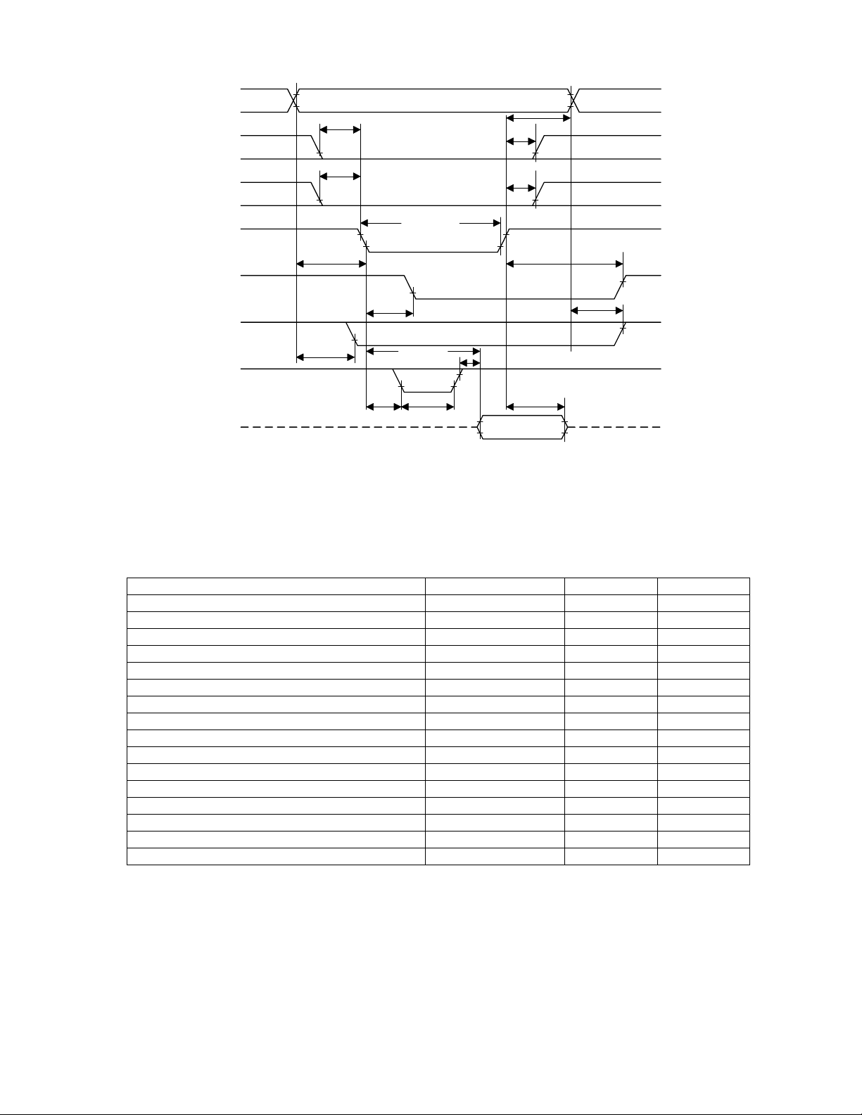
t
SMCLK
per
SMCLK
tsuSMD
SMD[15:0]
DATADATA
tdSMA
SMA[13:0]
SMDQM[1:0]
ROW ADDR
ROW ADDR
COLUMN ADDR
tdSMNCS
SMNCS[1:0]
SMNWE
ACTIVEACTIVE
tdSMCKE
SMCKE
tdSMNRAS
SMNRAS
tdSMNCAS
SMNCAS
Figure 6. System Memory Interface 'Read' Timing Diagram
thSMD
CS22220 Wireless PCMCIA Controller 25 of 34 DS557PP2 Rev. 3.0
www.cirrus.com
Page 26

Table 8. ROM/Flash Memory ‘Read’ Timing
Item Symbol
Clock Period
CE to SMD Latched Data
OE de-asserted to OE asserted
ROM address to output delay
(1)
(2)
(3)
(4)
SMCLK to SMA output delay
SMCLK to BRCE output delay (CE)
SMCLK to SMRAS output delay (OE)
SMD setup to SMCLK
SMD hold from SMCLK
t
SMCLK 72 MHz 103 MHz
per
tidSMD 221 ns
tfSMRAS 6(t
t
ACC
t
SMA 4.0 ns
d
BRCE 4.5 ns
t
d
t
SMRAS 5.0 ns
d
t
SMD 1.0 ns
su
t
SMD 2.4 ns
h
1. The memclock timing is derived by bootstrap PLL settings. Synchronous modes at 77 MHz & 72
MHz are currently supported.
SMD is based on the fm_romrdlat register settings – default is 09h max. (77Mhz ~ 17 times
2. t
id
SMCLK = 221ns).
SMRAS is the minimum time required before the next OE is active on the bus (6 times SMCLK).
3. t
f
The ROM device must release the bus within this time frame (77MHz ~ 78 ns).
4. Based on default fm_romrdlat register settings (note: 09h translates to 11h) see fm_romrdlat register
settings for more information)
Min Max
SMCLK)
per
220 ns
SMCLK
SMD[7:0]
SMA[11:0], SMD[13:8]
SMNWE
BRCE (CE)
SMRAS (OE)
SMCLK
t
per
SMD
t
ld
SMD
SMD
t
t
su
t
ACC
h
DATA
SMA
t
d
ADDRESS
BRCE
t
d
SMRAS
t
d
Figure 7. ROM Memory Interface 'Read' Timing Diagram
BRCE
t
d
SMRAS
t
d
SMRAS
t
f
CS22220 Wireless PCMCIA Controller 26 of 34 DS557PP2 Rev. 3.0
www.cirrus.com
Page 27

5.2 PCMCIA Interface Timing Diagrams
t
(R)
t
w
(WT)
c
(WT)
t
v
PC_A[25:0], PC_NREG
PC_NCE
PC_NOE
PC_NWAIT
PC_D[15:0]
t
(A) th(A)
a
(CE)
t
a
t
(CE)
su
(A) ta(OE)
t
su
(WT-OE)
t
v
(OE)
t
en
Figure 8. Attribute/Common Memory ‘Read’ Timing Diagram
Table 9. Common Memory ‘Read’ Timing Specification
t
h
(CE)
(A)
t
v
(CE)
t
dis
(OE)
t
dis
100 nsSpeed Version
Item
Read Cycle Time
Symbol
t
R 100
c
Min Max
Address Accesss Time ta(A) 100
Card Enable Access Time ta(CE) 100
Output Enable Access Time ta(OE) 50
Output Disable Time from PC_NOE t
(OE) 50
dis
Output Disable Time from PC_NCE ten(CE) 5
Data Valid from Address Change tv(A) 0
Address Setup Time tsu(A) 10
Address Hold Time th(A) 15
Card Enable Setup Time tsu(CE) 0
Card Enable Hold Time th(CE) 15
PC_NWAIT Valid from PC_NOE tv(WT-OE) 35
PC_NWAIT Pulse Width tw(WT) 12 us
Data Setup for PC_NWAIT Released tv(WT) 0
CS22220 Wireless PCMCIA Controller 27 of 34 DS557PP2 Rev. 3.0
www.cirrus.com
Page 28
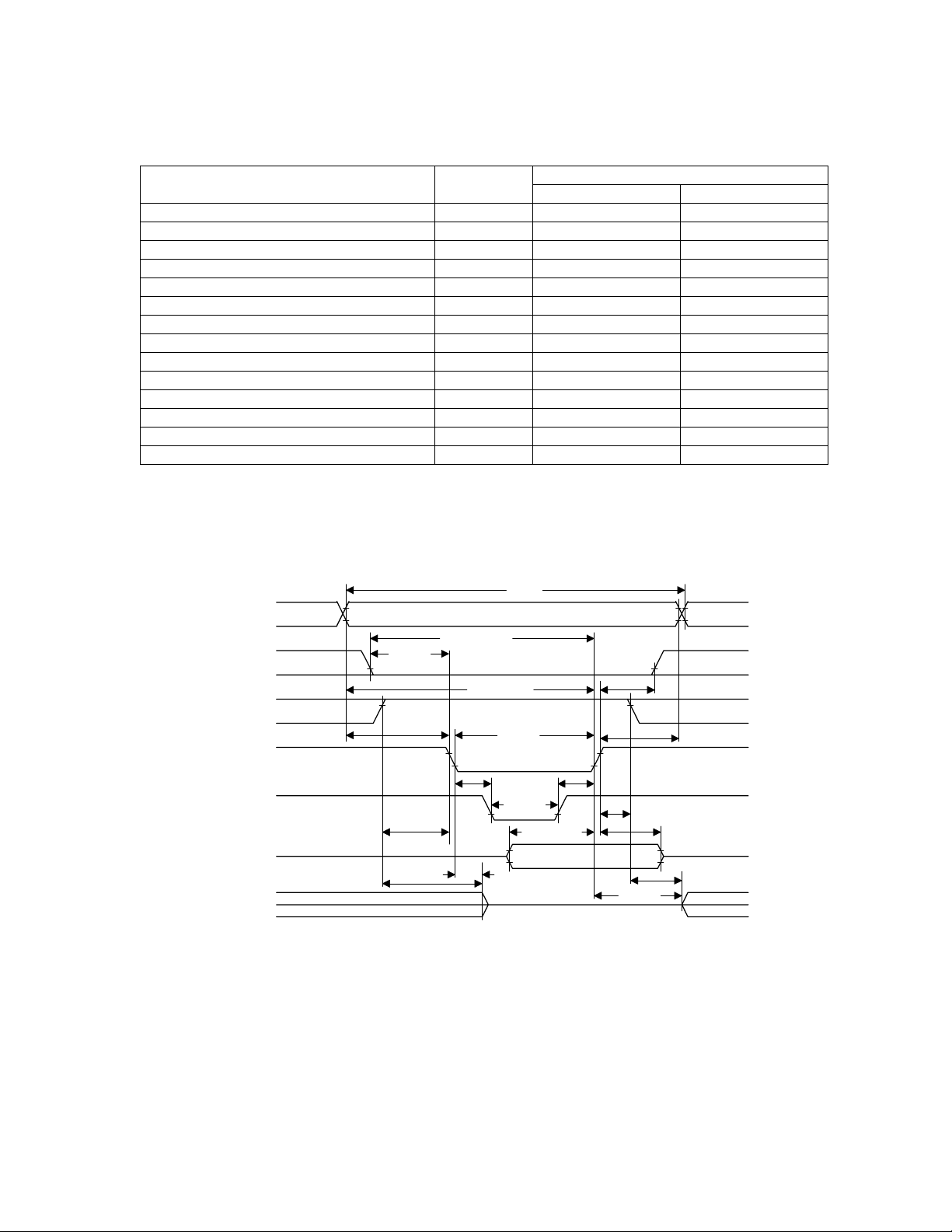
Table 10. Attribute Memory ‘Read’ Timing Specification
600 nsSpeed Version
Item
Read Cycle Time
Symbol
t
R 600
c
Min Max
Address Accesss Time ta(A) 600
Card Enable Access Time ta(CE) 600
Output Enable Access Time ta(OE) 300
Output Disable Time from PC_NOE t
(OE) 150
dis
Output Enable Time from PC_NCE ten(OE) 5
Data Valid from Address Change tv(A) 0
Address Setup Time tsu(A) 100
Address Hold Time th(A) 35
Card Enable Setup Time tsu(CE) 0
Card Enable Hold Time th(CE) 35
PC_NWAIT Valid from PC_NOE tv(WT-OE) 100
PC_NWAIT Pulse Width tw(WT) 12 us
Data Setup for PC_NWAIT Released tv(WT) 0
(W)
t
c
PC_A[25:0], PC_NREG
t
(CE-WEH)
PC_NCE
PC_NOE
PC_NWE
PC_NWAIT
PC_D[15:0](Din)
PC_D[15:0](Dout)
t
su
t
su
(OE-WE)
t
su
(OE)
t
dis
(CE)
(A)
su
t
(A-WEH)
su
(WE)
t
w
tv(WT-WE) tv(WT)
(WT)
t
w
tsu(D-WEH)
t
(WE)
dis
Valid Data Input
th(CE)
ten(WE)
(WE)
t
rec
th(OE-WE)
th(D)
ten(OE)
Figure 9. Memory ‘Write’ Timing Diagram
CS22220 Wireless PCMCIA Controller 28 of 34 DS557PP2 Rev. 3.0
www.cirrus.com
Page 29

Table 11. Common Memory ‘Write’ Timing Specification
100 nsSpeed Version
Item
Symbol
Min Max
Write Cycle time tcW 100
Write Pulse Width tw(WE) 60
Address Setup Time tsu(A) 10
Address Setup Time for PC_NWE tsu(A-WEH) 70
Card Enable Setup Time for PC_NWE tsu(CE-WEH) 70
Data Setup time for PC_NWE tsu(D-WEH) 40
Data Hold Time th(D) 15
Write Recovery Time t
Output Disable Time from PC_NWE
Output Disable Time from PC_NOE t
(WE) 15
rec
(WE)
t
dis
(OE) 50
dis
Output Enable Time from PC_NWE ten(WE) 5
Output Enable Time from PC_NOE ten(OE) 5
Output Enable Setup from PC_NWE tsu(OE-WE) 10
Output Enable Hold from PC_NWE th(OE-WE) 10
Card Enable Setup Time tsu(CE) 0
Card Enable Hold Time th(CE) 15
PC_NWAIT Valid from PC_NWE tv(WT-WE) 35
PC_NWAIT Pulse Width tw(WT) 12 us
PC_NWE High from PC_NWAIT Released 0
Table 12. Attribute Memory ‘Write’ Timing Specification
50
600 nsSpeed Version
Item
Symbol
Min Max
Write Cycle time tcW 600
Write Pulse Width tw(WE) 300
Address Setup Time tsu(A) 50
Address Setup Time for PC_NWE tsu(A-WEH) 350
Card Enable Setup Time for PC_NWE tsu(CE-WEH) 300
Data Setup time for PC_NWE tsu(D-WEH) 150
Data Hold Time th(D) 70
Write Recovery Time t
Output Disable Time from PC_NWE
Output Disable Time from PC_NOE t
(WE) 70
rec
(WE)
t
dis
(OE) 150
dis
150
Output Enable Time from PC_NWE ten(WE) 5
Output Enable Time from PC_NOE ten(OE) 5
Output Enable Setup from PC_NWE tsu(OE-WE) 35
Output Enable Hold from PC_NWE th(OE-WE) 35
Card Enable Setup Time tsu(CE) 0
Card Enable Hold Time th(CE) 35
PC_NWAIT Valid from PC_NWE tv(WT-WE) 100
PC_NWAIT Pulse Width tw(WT) 12 us
PC_NWE High from PC_NWAIT Released 0
CS22220 Wireless PCMCIA Controller 29 of 34 DS557PP2 Rev. 3.0
www.cirrus.com
Page 30
PC_A[25:0]
PC_NREG
PC_NCE
PC_NIORD
PC_NINPACK
PC_IOIS16
t
df
PC_NWAIT
PC_D[15:0]
IOIS16 (ADR)
t
A (IORD)
tsuREG (IORD)
CE (IORD)
t
su
t
t
A (IORD)
su
td(IORD)
h
REG (IORD)
t
h
CE (IORD)
t
h
(IORD)
w
INPACK (IORD)
t
df
t
(WT)
dr
tw(WT)
tdrINPACK (ADR)
Figure 10. I/O ‘Read’ Timing Diagram
tdrIOIS16 (ADR)
t
(IORD)tdfWT (IORD)
h
Table 13. I/O ‘Read’ (Input) Timing Specification
Item Symbol Min Max
(IORD) 100
Data Delay after PC_NIORD
Data Hold following PC_NIORD th(IORD) 0
PC_NIORD Width Time twIORD 165
Address Setup before PC_NIORD tsuA (IORD) 70
Address Hold following PC_NIORD thA(IORD) 20
PC_NCE Setup before PC_NIORD tsuCE (IORD) 5
PC_NCE Hold following PC_NIORD thCE (IORD) 20
PC_NREG Setup before PC_NIORD tsuREG (IORD) 5
PC_NREG Hold before PC_NIORD thREG (IORD) 0
PC_NINPACK Delay Falling from PC_NIORD tdfINPACK (IORD) 0 45
PC_NINPACK Delay Rising from PC_NIORD tdrINPACK (IORD) 45
PC_NIOIS16 Delay Falling from Address tdfIOIS16 (ADR) 35
PC_NIOIS16 Delay Rising from Address tdrIOIS16 (ADR) 35
PC_NWAIT Delay Falling from PC_NIORD tdWT (IORD) 35
Data Delay from PC_NWAIT Rising tdr(WT) 0
PC_NWAIT Width Time tw(WT) 12,000
t
d
CS22220 Wireless PCMCIA Controller 30 of 34 DS557PP2 Rev. 3.0
www.cirrus.com
Page 31

PC_A[25:0]
PC_NREG
PC_NCE
PC_NIOWR
PC_IOIS16
t
df
PC_NWAIT
PC_D[15:0]
tsuREG (IOWR)
t
CE (IOWR)
su
t
(IOWR)
w
A(IOWR)
t
su
IOIS16 (ADR) tdfWT (IOWR)
t
w
t
(IOWR)
su
Figure 11. I/O ‘Write’ Timing Diagram
A(IOWR)
t
h
t
REG (IOWR)
h
CE (IOWR)
t
h
(WT)
tdrIOWR (WT)
t
t
IOIS16 (ADR)
dr
(IOWR)
h
Table 14. I/O ‘Write’ (Output) Timing Specification
Item Symbol Min Max
(NIOWR) 60
Data Setup after PC_NIOWR
Data Hold following PC_NIOWR th(NIOWR) 30
PC_NIOWR Width Time twIOWR 165
Address Setup before PC_NIOWR tsuA (NIOWR) 70
Address Hold following PC_NIOWR thA (NIOWR) 20
PC_NCE Setup before PC_NIOWR tsuCE (NIOWR) 5
PC_NCE Hold following PC_NIOWR thCE (NIOWR) 20
PC_NREG Setup before PC_NIOWR tsuREG (NIOWR) 5
PC_NREG Hold following PC_NIOWR thREG (NIOWR) 0
PC_NIOIS16 Delay Falling from Address tdfIOIS16 (ADR) 35
PC_NIOIS16 Delay Rising from Address tdrIOIS16 (ADR) 35
PC_NWAIT Delay Falling from PC_NIOWR tdWT (NIOWR) 35
PC_NWAIT Width Time tw(WT) 12,000
PC_NIOWR Width Time tdrIOWR (WT) 0
t
d
CS22220 Wireless PCMCIA Controller 31 of 34 DS557PP2 Rev. 3.0
www.cirrus.com
Page 32

Table 15. Radio MAC AC Timings – Intersil Modes
Parameter Parameter Description Min Max Units
tdBBAS BBAS output delay from falling BBSCLK 8.2 ns
tdBBRNW BBRNW output delay from falling BBSCLK 8.0 ns
tdnBBCS nBBCS output delay from falling BBSCLK 59.0 ns
tdBBSDX BBSDX output delay from falling BBSCLK 7.0 ns
TsuBBSDX BBSDX setup to rising edge of BBSCLK 14.8 ns
ThBBSDX BBSDX hold from rising edge of BBSCLK 0.0 ns
tdTXD TXD output delay from rising TXCLK (SMAC
Mode)
tdTXD TXD output delay from rising TXCLK (RMAC
Mode)
TsuRXD RXDsetuptorisingedgeofRXCLK 1.0 ns
ThRXD RXD hold from rising edge of RXCLK 1.8 ns
TsuMDRDY MDRDY setup to falling edge of RXCLK 2 ns
ThMDRDY MDRDY hold from falling edge of RXCLK 1 ns
tdTXPEBB TXPEBB output delay from rising TXCLK 15.0 ns
tdRXPEBB RXPEBB output delay from rising RXCLK 16.0 ns
TsuTXRDY TXRDY setup to falling edge of TXCLK 6.5 ns
ThTXRDY TXRDY hold from falling edge of TXCLK 0 ns
T
duty
T
duty
RXCLK
TXCLK
2
2
RXCLK period See Note ns
TXCLK period See Note ns
33.5 ns
15.4 ns
Notes:
1. CCA signal is double synchronized to ARMCLKIN.
2. ARMCLK must be at least 4 times the TXCLK and RXCLK frequency.
3. Harris baseband (3824/3824A) generates RXCLK and TXCLK of 4 Mhz. the duty cycle varies between 33-40%
with a high time of 90.9ns and low time that alternates between 136 and 182ns. The clock period varies between
227 and 272 ns, giving an effective period of 250ns.
4. TXD delay in 802.11b mode is the result of sampling the TXCLK with the ctlclk, therefore the maximum delay
is equal to two ctlclk periods plus the flop-to-output delay. In this table, ctlclk is assumed to have a 13 ns
period.
5. BBNCS output delay = [(1/ARMCLK freq)*ceiling(SER_CLK_DIV/2)] + 7ns, the specified value is based on
ARMCLK of 77 Mhz and SER_CLK_DIV=8.
CS22220 Wireless PCMCIA Controller 32 of 34 DS557PP2 Rev. 3.0
www.cirrus.com
Page 33

Table 16. Radio MAC AC Timings – RFMD Modes
Parameter Parameter Description Min Max Units
tdBBRNW BBRNW output delay from falling BBSCLK 6.7 ns
tdnBBCS nBBCS output delay from falling BBSCLK 110.79 ns
tdBBSDX BBSDX output delay from falling BBSCLK 7.0 ns
TsuBBSDX BBSDX setup to rising edge of BBSCLK 14.5 ns
ThBBSDX BBSDX hold from rising edge of BBSCLK 0.0 ns
tdTXD TXD output delay from rising TXCLK (SMAC
Mode)
tdTXD TXD output delay from rising TXCLK (RMAC
Mode)
TsuRXD RXDsetuptorisingedgeofRXCLK 1.0 ns
ThRXD RXD hold from rising edge of RXCLK 1.8 ns
TsuMDRDY MDRDY setup to falling edge of RXCLK 2 ns
ThMDRDY MDRDY hold from falling edge of RXCLK 1 ns
tdTXPEBB TXPEBB output delay from rising TXCLK 15.0 ns
tdRXPEBB RXPEBB output delay from rising RXCLK 16.0 ns
TsuTXRDY TXRDY setup to falling edge of TXCLK 6.5 ns
ThTXRDY TXRDY hold from falling edge of TXCLK 0 ns
Notes:
1. CCA signal is double synchronized to ARMCLKIN.
2. ARMCLK must be at least 4 times the TXCLK and RXCLK frequency.
3. TXD delay in 802.11b mode is the result of sampling the TXCLK with the ctlclk, therefore the maximum delay
is equal to two ctlclk periods plus the flop-to-output delay. In this table, ctlclk is assumed to have a 13 ns
period.
4. BBNCS output delay = [(1/ARMCLK freq)*ceiling(SER_CLK_DIV/2)] + 7ns, the specified value is based on
ARMCLK of 77 Mhz and SER_CLK_DIV=8.
33.5 ns
15.4 ns
Table 17. Package Specifications
Symbol Parameter Value Units
θ
JC
Junction-to-Case Thermal
Resistance
θ
JA
Junction-to-Open Air Thermal
Resistance
T
J_MAX
Max Junction Temperature 105
Notes:
1. ARMCLK / MEMCLK = 77MHz
CS22220 Wireless PCMCIA Controller 33 of 34 DS557PP2 Rev. 3.0
www.cirrus.com
2.5
26.9
°C/W
°C/W
°C
Page 34

6 Packaging
The CS22220 Controller is available in a 208 Fine Pitch Ball Grid Array (FPBGA) package.
Figure 12 contains the package mechanical drawing.
Figure 12. CS22220 208 FPBGA-pin Mechanical Drawing
CS22220 Wireless PCMCIA Controller 34 of 34 DS557PP2 Rev. 3.0
www.cirrus.com
 Loading...