

CS22210 Data Sheet
p
m
Wireless PCI/USB Controller
1 Description
The Cirrus Logic CS22210 Wireless Network Controller enables high speed, 11 Mbps digital wireless
data connectivity for wireless data connectivity for PCI, mobile, embedded systems and other cost
sensitive applications.
The CS22210 is a highly integrated single-chip PCI / USB solution for wireless networks supporting video,
audio, voice, and data traffic. The programmable controller executes Cirrus Logic’s Whitecap™2
networking protocol that provides Wi-Fi™ (802.11b) compliance as well as multimedia and quality of
service (QoS) support. The device includes several high performance components including an
ARM7TDMI RISC processor core, a Forward Error Correction (FEC) codec and a wireless Radio MAC
supporting up to11 Mbps throughput. The CS22210 is designed to support both a standard PCI 2.1 or
PCI 2.2 compliant interface or USB 1.1 compliant device interface making it an ideal choice for cost
effective standalone and embedded high-speed wireless networking products.
The CS22210 utilizes state-of-the-art 0.18um CMOS process and is housed in a 208 MQFP package
designed to provide integrated low cost IEEE 802.11 standard compliant system solutions. The core is
powered at 1.8 V to reduce overall power consumption. In addition, the CS22210 supports various power
management modes for host, MAC, baseband, and radio interfaces.
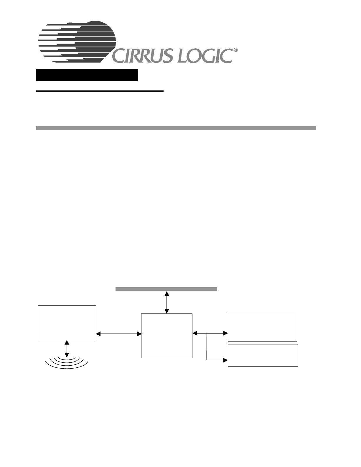
Figure 1. Example System Block Diagram
PCIorUSBHost
Networking Data
802.11b compatible
2.4 GHz
Digital Radio
PHY Transceiver
2.4 GHz Direct Sequence
S
read Spectru
CS22210 PCI/USB Wireless Controller 1 of 31 D556PP2 Rev. 3.0
11 Mbps
Wireless
Baseband I/F
CS22210
Wireless
Network
Controller
www.cirrus.com
System Memory
SDRAM (Up to 4MB)
SRAM (Up to 256KB)
Boot ROM/Flash
(Upto1MB)

2 Features
Embedded ARM Core and System Support Logic
• High performance ARM7TDMI RISC processor core at 77MHz
• 4KB integrated, one-way set associative, unified, write through cache
• Individual interrupt for each functional block
• Two 23-bit programmable (periodic or one-shot) general purpose timers
• 8 Dword (32-bits) memory write and read buffers for high system performance
• Abort cycle detection and reporting for debugging
• ARM performance monitoring function for system fine-tuning
• Programmable performance improvement logic based on system configuration
• Flexible independent DMA engines for PCI, USB and digital radio functional units
Enhanced Memory Controller Unit
• Programmable memory controller unit supporting SDRAM /async SRAM/boot ROM interface
• 16-bit data bus with 12-bit address supporting up to 4MB at up to 103MHz SDRAM
• 8-bit data bus with addressing support up to 1MB of boot ROM/Flash
• Programmable SDRAM timing and size parameters such as CAS latencies and number of banks
columns and rows
FEC codec
• High performance Reed-Solomon coding for error correction (255:239 block coding)
• Reduces symbol error probability of a typical 10e-3 error rate environment to 10e-9
• Programmable rate FEC engine to optimize channel efficiency
• Low latency, fully pipelined hardware encoding and decoding. Support byte wise single cycle throughput
up to 77MHz, with a sustain rate of 77MBps.
• Double buffering (64 Dword read/write buffer) to enhance system performance
• On the fly configuration of encoder and decoder
Digital Wireless Radio MAC
• Standard interface to 802.11b radio baseband transceiver
• 11Mbps data rate
• 32 Dword transmit/receive FIFO
• Supports clear channel assessment (CCA)
Power Management
• Host (PCI or USB) ACPI compliant
• Remote USB host wakeup
• Supports variable rate radio transmit, receive and standby radio power modes through two DACs
Clock and PLL Interface
• Single 44MHz crystal oscillator reference clock for PCI version; 48MHz reference clock required in USB
option
• Internal PLL to generate internal and on board clocks
CS22210 PCI/USB Wireless Controller 2 of 31 D556PP2 Rev. 3.0
www.cirrus.com

PCI Controller Interface
• 33MHz 5V/3.3V PCI 2.1 and PCI 2.2 compliant master/target 32-bit data interface
• ARM communication with PCI controller through simple mailbox scheme
• Generic PCI controller programming interface
• Flexible configuration programming via EEPROM
USB Controller Interface
• 12 Mbps USB 1.1 compliant device
• Supports 1 to 16 endpoints; endpoints can be bulk, isochronous or interrupt
• Variable endpoint buffer depths providing maximum flexibility for endpoint configurations
• Flexible configuration programming via EEPROM or firmware download
• Remote host wakeup
Chip Processing and Packaging
• 208 MQFP package and 0.18 um state of the art CMOS process
• 1.8 V core for low power consumption; 3.3V I/O and 5V tolerant
IMPORTANT NOTICE
"Preliminary" product information describes products that are in production, but for which full characterization data is not yet available.
"Advance" product information describes products that are in development and subject to development changes. Cirrus Logic, Inc. and
its subsidiaries ("Cirrus") believe that the information contained in this document is accurate and reliable. However, the information is
subject to change without notice and is provided "AS IS" without warranty of any kind (express or implied). Customers are advised to
obtain the latest version of relevant information to verify, before placing orders, that information being relied on is current and complete.
All products are sold subject to the terms and conditions of sale supplied at the time of order acknowledgment, including those
pertaining to warranty, patent infringement, and limitation of liability. No responsibility is assumed by Cirrus for the use of this
information, including use of this information as the basis for manufacture or sale of any items, or for infringement of patents or other
rights of third parties. This document is the property of Cirrus and by furnishing this information, Cirrus grants no license, express or
implied under any patents, mask work rights, copyrights, trademarks, trade secrets or other intellectual property rights. Cirrus owns the
copyrights of the information contained herein and gives consent for copies to be made of the information only for use within your
organization with respect to Cirrus integrated circuits or other parts of Cirrus. This consent does not extend to other copying such as
copying for general distribution, advertising or promotional purposes, or for creating any work for resale.
An export permit needs to be obtained from the competent authorities of the Japanese Government if any of the products or
technologies described in this material and controlled under the "Foreign Exchange and Foreign Trade Law" is to be exported or taken
out of Japan. An export license and/or quota needs to be obtained from the competent authorities of the Chinese Government if any of
the products or technologies described in this material is subject to the PRC Foreign Trade Law and is to be exported or taken out of the
PRC.
CERTAIN APPLICATIONS USING SEMICONDUCTOR PRODUCTS MAY INVOLVE POTENTIAL RISKS OF DEATH, PERSONAL
INJURY, OR SEVERE PROPERTY OR ENVIRONMENTAL DAMAGE ("CRITICAL APPLICATIONS"). CIRRUS PRODUCTS ARE NOT
DESIGNED, AUTHORIZED, OR WARRANTED TO BE SUITABLE FOR USE IN LIFE-SUPPORT DEVICES OR SYSTEMS OR OTHER
CRITICAL APPLICATIONS. INCLUSION OF CIRRUS PRODUCTS IN SUCH APPLICATIONS IS UNDERSTOOD TO BE FULLY AT
THE CUSTOMER'S RISK.
Cirrus Logic, Cirrus, and the Cirrus Logic logo designs are trademarks of Cirrus Logic, Inc. All other brand and product names in this
document may be trademarks or service marks of their respective owners.
Use of this product in any manner that complies with the MPEG-2 video standard as defined in ISO
documents IS 13818-1 (including annexes C, D, F, J, and K), IS 13818-2 (including annexes A, B, C, and D,
but excluding scalable extensions), and IS 13818-4 (only as it is needed to clarify IS 13818-2) is expressly
prohibited without a license under applicable patents in the MPEG-2 patent portfolio, which license is
available from MPEG LA, L.L.C. 250 Steele Street, Suite 300, Denver, Colorado 80296.
CS22210 PCI/USB Wireless Controller 3 of 31 D556PP2 Rev. 3.0
www.cirrus.com
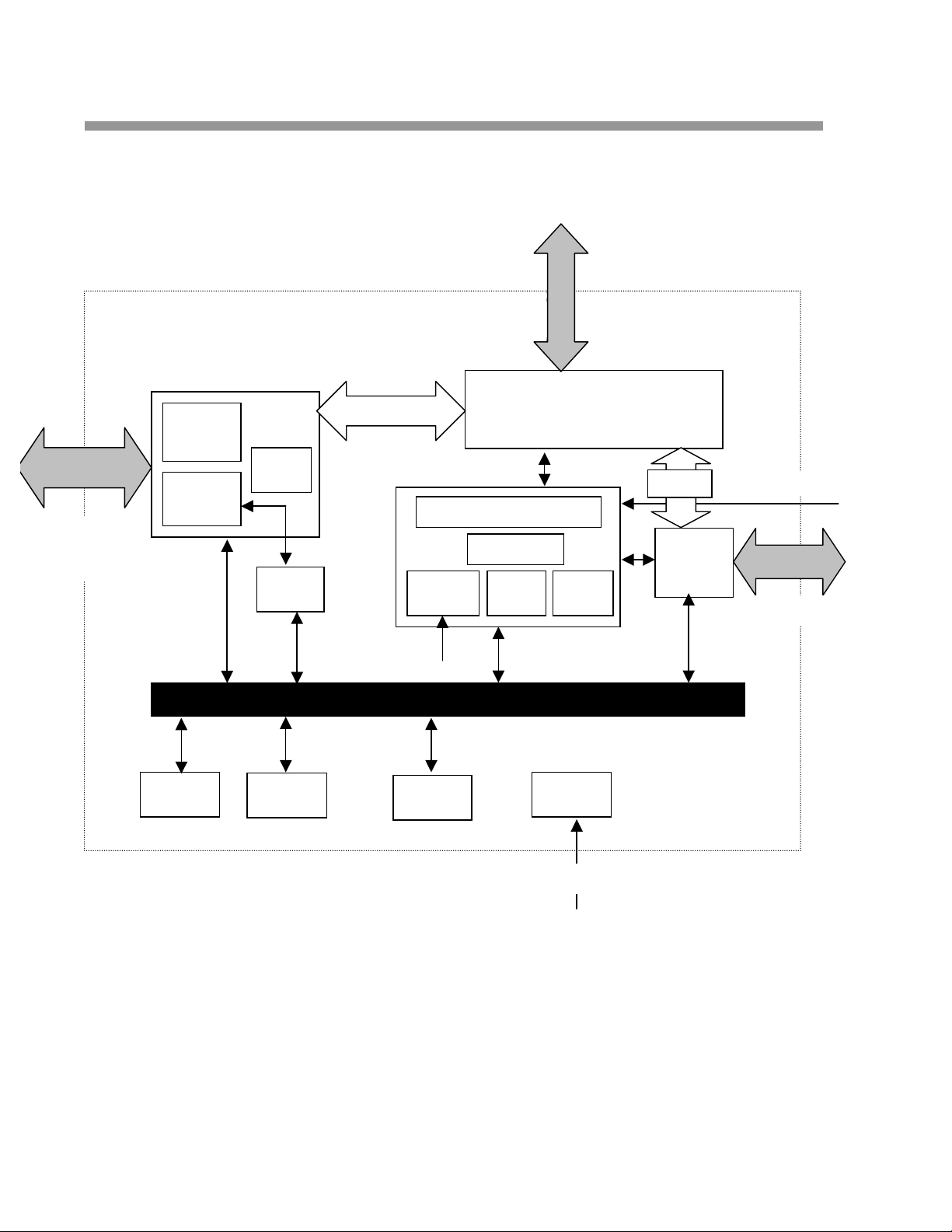
3 Functional Description
y
y
Figure 2. Block Diagram of Major Functional Units
PCI
Interface
stem Memor
System Memory
S
Memory/Boot ROM
Controller
Arbiter
USB or PCI
Host Interface
12MHz
or
33 MHz
USB
Interface
Sleep
Timer
DMA
CTRL
Comm
Buffer
FEC
CODEC
Read/Write Buffer
ARM 7TDMI
Interrupt
controller
77MHz System Control Bus
Misc.
Config.
Timer
(2)
48MHz / 44 MHz
4KB
Cache
Clock/PLL
DMA
Dual Radio
MAC
W/ DMA Ctrl
JTAG/Test Interface
Radio
Interface
44MHz
Crystal
or
Oscillator
CS22210 PCI/USB Wireless Controller 4 of 31 D556PP2 Rev. 3.0
www.cirrus.com

3.1 Embedded ARM Core and System Support Logic
The processing elements of the CS22210 include the ARM7TDMI core and its associated
system control logic. The ARM processor and system controller consist of a memory
management unit, 4-KB write through cache controller, 20 IRQ and 4 FIRQ interrupt
controller, and 2 general purpose timers. The ARM processor and integrated system support
logic provide the necessary execution engine to support a real time multi-tasking operating
system, the network protocol stack, and firmware services. In addition, system performance
monitor logic is included to aid in system performance fine-tuning (e.g. cache hit, CPI
numbers).
Memory Management Unit
ARM instructions and data are fetched from system memory a cache-line (4/8 – Dwords
/Programmable) at a time when caching is turned on. During a cache line fill, critical word
data, i.e., the access that caused the miss, is forwarded to the ARM and also written into the
data RAM cache. The non-critical words in the line fetched following the critical word are then
written to the cache on a Dword basis, as they become available.
Memory writes are posted to dual 4-Dwords (32-bit) memory write posting buffers. Write
posts use the sequential addressing feature on the memory bus. With dual buffering an out of
sequence write will post to one write buffer while the other buffer is flushed to memory.
There is one 8Dword Read Buffer in the MEM block. The buffer is used for both cacheable
and non-cacheable memory space.
Interrupt Controller
The interrupt controller provides two interrupt channels to the ARM processor. One interrupt
channel is presented to the ARM on its nFIQ, and the other channel is presented on its nIRQ
pin. These are referred to as the FIQ channel and the IRQ channel. Both channels operate
in identical but independent fashion. The FIQ channel has a higher priority on the ARM
processor than the IRQ channel.
The interrupt controller includes a CONTROL register for each logical interrupt in the ARM
complex. The CONTROL register serves the following main purposes:
• Provides the mapping between the EXT_INT inputs (physical interrupts) and the logical
interrupt
• Selects the particular type of signaling expected on the EXT_INT inputs: level, edge,
active level high/low etc.
• Enables or disable a logical interrupt
CS22210 PCI/USB Wireless Controller 5 of 31 D556PP2 Rev. 3.0
www.cirrus.com

3.2 Digital Wireless Radio Interface
The CS22210 digital radio MAC I/F supports multiple radio baseband and RF interfaces. The
baseband registers can be programmed during the configuration time using the control port
interface. The MAC also provides the capability of programming the signal, service and
length on per packet basis without ARM intervention. This significantly improves the
performance of the system.
There are three primary digital interface ports for the CS22210 that are used for configuration
and during normal operation.
These ports are:
• The Control Port, which is used to configure, set power consumption modes, write and/or
read the status of the radio base band registers.
• The TX Port, which is used to output the data that needs to be transmitted from the
network processor.
• The RX Port, which is used to input the received demodulated data to the network
processor.
3.3 FEC Codec
The FEC codec performs Reed-Solomon code encoding to protect the data before it is
transmitted to a noisy channel. It is a similar code as employed by digital broadcast industry,
such as ITU-T J.83 for DVB. The RS(255, 239) code implemented by the SWG2710 can
reduce error probability to 1/10e-9 in a typical 1/10e-3 error rate environment. The
encoder/decoder can be programmed to vary the coding block length (N) and correctable
error (t) to optimize the tradeoff between channel utilization and data protection. The range of
N iscurrentlysettobefrom50to255,andthet is 8. The symbol size is fixed at 8 bits.
Coding parameters can be set real time, allowing maximum flexibility for the system to adjust
the FEC setting, such as block size, in order to optimize channel efficiency. The encoder also
has a very low latency of two cycles. Both the encoder and decoder are fully pipelined in
structure to achieve single cycle throughput. The FEC can be disabled in firmware.
CS22210 PCI/USB Wireless Controller 6 of 31 D556PP2 Rev. 3.0
www.cirrus.com

3.4 Programmable Memory Controller
The CS22210 incorporates a general purpose memory controller that supports a
SDRAM/async SRAM memory and FLASH memory interface.
In the RAM configuration, the system memory interface supports up to 16-Mbyte of 16-bit
SDRAM running at a frequency up to 103 MHz single-state access cycles or 256KB of 16 bit
async SRAM. The memory controller provides programming of SDRAM parameters such as
CAS latency, refresh rate etc; these registers are located in miscellaneous configuration
registers. When there are no pending memory requests from any internal requester, the
CS22210 will keep Clock Enable (CKE) signal low to cause the SDRAM to stay in power
down mode. Once a memory request is active, the CS22210 will assert CKE high to cause
the SDRAM to come out of power down mode. Typically, this can reduce memory power
consumption by up to 50%.
In ROM configuration, firmware for CS22210 is stored in non-volatile memory and is
accessed through the Boot ROM interface. The maximum addressable ROM space
supported is 1MB. ROM read/write and output enable are shared with RAM control pins. The
ROM can be re-flashed allowing for software upgrades.
3.5 PCI Controller Interface
Embedded in the CS22210 is a PCI 2.1 / PCI 2.2 fully compliant master/target 32 bit data
interface including power management support (PME signal). The communication buffer
logic was designed to be flexible and generic to both the PC software and ARM firmware.
The control communication between PCI and ARM uses a mailbox mechanism. The PCI
writes data into a Dword mailbox register whereby an interrupt is generated to the ARM. The
ARM reads this register to get the control information whereby an interrupt is generated to the
PCI. The same is true from the ARM writing to a ARM mailbox register.
PCI data transfer is supported by a DMA Control Block (DCB). The DCB is configured by the
ARM, allowing the ARM to control how often it is interrupted. PCI data transfers are done by
the PCI master and the DCB offloading CPU overhead.
3.6 USB Interface
Embedded within the CS22210 is a full speed USB 1.1 compliant device interface. The
device supports from 1 to 16 endpoints and is completely programmable via firmware
download or external EEPROM.
All “setup” commands are passed to the system processor for interpretation. The device also
contains a DMA engine to transfer arbitrary amounts of data to and from main memory before
interrupting the system processor.
CS22210 PCI/USB Wireless Controller 7 of 31 D556PP2 Rev. 3.0
www.cirrus.com

4 Pinout and Signal Descriptions
K
System
Memory
Interface
JTAG Interface
System and PCI Reset
Clock Interface
PLL Power
Interface
Figure 3. CS22210 Logical Pin Groupings (note: not all signals are shown)
SMCLK
nSMCS[1:0]
nSMRAS
nSMCAS
nSMWE
SMDQM[1:0]
SMCKE
SMA[11:0]
SMD[15:0]
nBRCE
nTRST
nRST
XTALCLKIN
XTALOUT
XTRACLK
PLLAGND
PLLAVCC
PLLDVCC
PLLDGND
PLLPLUS
USB_ENUM
TDO
TDI
TCK
TMS
nPERR, nSERR
CS22210
Wireless
Network
Controller
nSERR
nPERR
PCLK
AD[31:0]
nCBE[3:0]
IDSEL
nFRAME
nIRDY
nTRDY
nDEVSEL
nSTOP
NRST
NINTA
PME
nRST
nREQ
nGNT
PARX
SYNTH_LE1
SYNTH_LE2
TXCLK
TXPE
TXD
TXRDY
CCA
BBRNW
nRESETBB
BBAS
nBBCS
TXPAPE
TXPEBB
RXPEBB
BBSCLK
BBSDX
PCI Controller
Interface
Digital Wireless Radio
USB
Interface
DACAVCC & DACAGND
USBVPX
USBVMX
NTEST
nRPD
RXCL
MDRDY
RXD
CS22210 PCI/USB Wireless Controller 8 of 31 D556PP2 Rev. 3.0
www.cirrus.com

This section provides detailed information on the CS22210 signals. The signal descriptions are
useful for hardware designers who are interfacing the CS22210 with other devices.
System Memory Interface
The system memory interface supports standard SDRAM interface, async SRAM and FLASH.
There are total of 37 signals in this interface.
SMCLK Output
System mem clock for SDRAM. Currently the interface supports 103 MHz
for a maximum bandwidth of 200Mbytes/sec.
nSMCS0 Output
Chip select bit 0. This signal is used to select or deselect the SDRAM for
command entry. When SMNCS is low it qualifies the sampling of
nSMRAS, nSMCAS and nSMWE. Also used as testmode(2) when NTEST
pin is '0'.
nSMCS Output
Chip select bit 1.
nBRCE Output
Chip select for ROM access. This signal is used to select or deselect the
boot ROM memory.
nSMRAS Output
Row address select. Used in combination with nSMCAS, nSMWE and
nSMCS to specify which SDRAM page to open for access. Also used
during reset to latch in the strap value for clk_bypass; if set to a '1' implies
bypassing clock module; whatever clk is applied on the input clock is used
for memclk and ctlclk. Also shared as the ROMOE signal.
NSMCAS Output
Column address select. Used in combination with nSMRAS, nSMWE and
nSMCS to specify which piece of data to access in selected page. Also
used during reset to latch in the strap value for same_freq; if set to a '1'
implies internal mem_clk and arm_clk are running at the same frequency
and 180 degrees out of phase.
CS22210 PCI/USB Wireless Controller 9 of 31 D556PP2 Rev. 3.0
www.cirrus.com

nSMWE Output
Write enable is used in combination with nSMRAS, nSMCAS, and
nSMWE to specify whether the current cycle is a read or a write cycle.
Also used during reset to latch in the strap value for tst_bypass; if set to a
'1' implies PLL bypass. Also shared as the ROMWE to do flash
programming.
SMDQM[1:0] Output
Data mask bit 1:0. These signals function as byte enable lines masking
unwanted bytes on memory writes. Also used as testmode(1:0) when
NTEST pin is '0'.
SMCKE Output
Clock enable. SMCKE is used to enable and disable clocking of internal
RAM logic.
SMA0 Output
Address bit0. The address bus specifies either the row address or column
address. Also shared as boot-rom address bit0. This pin should be pulldown.
SMA1 Output
Address bit1. Also shared as boot-rom address bit1. Also used during
reset to latch in the strap value for pcisel; if set to a '1' implies pci mode.
SMA2 Output
Address bit2. Also shared as boot-rom address bit2. Also used during
reset to latch in the strap value for usbsel; if set to a '1' implies usb mode.
SMA3 Output
Address bit3. Also shared as boot-rom address bit3. This pin should be
pull-down.
SMA4 Output
Address bit4. Also shared as boot-rom address bit4. Also used during
reset to latch in the strap value for romcfg; if set to a '1' implies pci
configuration data should be downloaded from ROM.
SMA5 Output
Address bit5. Also shared as boot-rom address bit5. Also used during
reset to latch in the strap value for test_rst_enb; if set to a '0' implies
normal operation mode.
CS22210 PCI/USB Wireless Controller 10 of 31 D556PP2 Rev. 3.0
www.cirrus.com

SMA6 Output
Address bit6. Also shared as boot-rom address bit6. Also used during
reset to latch in the strap value for freq_sel(0). Freq_sel(2:0) is used to
select the multiplication factor for the internal PLL (000=1x, and 111=8x).
SMA7 Output
Address bit7. Also shared as boot-rom address bit7. Also used during
reset to latch in the strap value for freq_sel(1). Freq_sel(2:0) is used to
select the multiplication factor for the internal PLL (000=1x, and 111=8x).
SMA8 Output
Address bit8. Also shared as boot-rom address bit8. Also used during
reset to latch in the strap value for freq_sel(2). Freq_sel(2:0) is used to
select the multiplication factor for the internal PLL (000=1x, and 111=8x).
SMA9 Output
Address bit9. Also shared as boot-rom address bit9. Also used during
reset to latch in the strap value for sdram_delay(0). Sdram_delay(2:0) is
used to select the delay factor for the internal memory clock (000=0ns,
and 111=1.75ns with each .25ns increments).
SMA10 Output
Address bit10. Also shared as boot-rom address bit10. Also used during
reset to latch in the strap value for sdram_delay(1). Sdram_delay(2:0) is
used to select the delay factor for the internal memory clock (000=0ns,
and 111=1.75ns with each .25ns increments).
SMA11 Output
Address bit11. Also shared as boot-rom address bit11. Also used during
reset to latch in the strap value for sdram_delay(2). Sdram_delay(2:0) is
used to select the delay factor for the internal memory clock (000=0ns,
and 111=1.75ns with each .25ns increments).
SMD[7:0] Bi-directional
Data bus. The data bus contains the data to be written to memory on a
writecycleandthereadreturndataonareadcycle.
SMD[15:8] Bi-directional
Shared data bus. The data bus contains the data to be written to RAM
memoryonawritecycleandthereadreturndataonareadcycle.Databit
[15:8] is also shared as boot ROM address bit [19:12].
CS22210 PCI/USB Wireless Controller 11 of 31 D556PP2 Rev. 3.0
www.cirrus.com

Digital Wireless Radio Interface
All radio input buffers are Schmitt triggered input buffers. There are total of 21 signals in this
interface.
TXCLK Input
Transmit clock is a clock input from the radio baseband processor. This
signal is used to clock out the transmit data on the rising edge of TXCLK.
TXPEBB Output
Baseband transmit power enable, an output from the MAC to the radio
baseband processor. When active, the baseband processor transmitter is
configured to be operational, otherwise the transmitter is in standby mode.
TXD Output
It is the serial data output from the MAC to the radio baseband processor.
The data is transmitted serially with the LSB first. The data is driven by the
MAC on the rising edge of TXCLK and is sampled by the radio baseband
processor on the falling edge of TXCLK (in 3824 mode) and rising edge of
TXCLK (in 3860B mode).
TXRDY Input
Transmit data ready is an input to the MAC from the radio baseband
processor to indicate that the radio baseband processor is ready to
receive the data packet over the TXD signal. The signal is sampled by the
MAC on the rising edge of TXCLK.
CCA Input
Clear channel assessment is an input from the radio baseband processor
to signal that the channel is clear to transmit. When this signal is a 0, the
channel is clear to transmit. When this signal is a 1, the channel is not
clear to transmit. This helps the MAC to determine when to switch from
receive to transmit mode.
BBRNW Output
Baseband read/write is an output from the MAC to indicate the direction of
the SD bus when used for reading or writing data. This signal has to be
set up to the rising edge of BBSCLK for the baseband processor and is
driven on the falling edge of BBSCLK.
NRESETBB Output
Baseband reset is an output of the MAC to reset the baseband processor.
CS22210 PCI/USB Wireless Controller 12 of 31 D556PP2 Rev. 3.0
www.cirrus.com

BBAS Output
Baseband address strobe is used to envelop the address or the data on
the BBSDX bus. Logic 1 envelops the address and a logic 0 envelops the
data. This signal has to be set up to the rising edge of BBSCLK for the
baseband processor and is driven on the falling edge of BBSCLK.
NBBCS Output
Baseband chip select is an active low output to activate the serial control
port. When inactive the SD, BBSCLK, BBAS and BBRNW signals are
‘don’t cares’.
TXPAPE Output
Radio power amplifier power enable is a software-controlled output. This
signal is used to gate power to the power amplifier.
TXPE Output
Radio transmit power enable indicates if transmit mode is enabled. When
low, this signal indicates receive mode.
RXPEBB Output
Baseband receive power enable is an output that indicates if the MAC is in
receive mode. This output to the baseband processor enables receive
mode in baseband processor.
BBSCLK Output
Baseband serial clock is a programmable output generated by dividing
ARM_CLK by 14 (default). This clock is used for the serial control port to
sample the control and data signals.
BBSDX Bi-directional
Baseband serial data is a bi-directional serial data bus, which is used to
transfer address and data to/from the internal registers of the baseband
processor.
SYNTHLE Output
Synthesizer latch enable is an active high signal used to send data to the
synthesizer.
SYNTH_LE1 Output
Synthesizer latch enable is an active high signal used to send data to the
synthesizer (RF LE).
SYNTH_LE2 Output
Synthesizer latch enable is an active high signal used to send data to the
synthesizer (IF LE).
CS22210 PCI/USB Wireless Controller 13 of 31 D556PP2 Rev. 3.0
www.cirrus.com

NRPD Output
Radio power down enable is an active low signal used for power
management purposes for the radio circuitry.
RXCLK Input
This is an input from baseband processor. It is used to clock in received
data from baseband processor.
MDRDY Input
Receive data ready is an input signal from the baseband processor,
indicating a data packet is ready to be transferred to the MAC. The signal
returns to inactive state when there is no more receiver data or when the
link has been interrupted. This signal is sampled on the falling edge of
RXCLK (in 3824 mode), and sampled at rising edge of RXCLK (in 3860B
mode).
RXD Input
Receive data is an input from the baseband processor transferring
demodulated header information and data in a serial format. The data is
frame aligned with MD_RDY. This signal is sampled on the falling edge of
RXCLK (in 3824 mode), and sampled at rising edge of RXCLK (in 3860B
mode).
DACAVCC Input
Analog power for DAC. 3.3V input.
DACAGND Input
Analog ground for DAC.
RLQ Output
Radio link quality based on packet error rate. Active low implies the
packet was received without errors. Note: Lost packets are not detected.
CS22210 PCI/USB Wireless Controller 14 of 31 D556PP2 Rev. 3.0
www.cirrus.com

PLL and Clock Interface
There are three clock pins and five PLL power pins. Total of 8 signals in this interface.
XTAL_CLKIN Input
44 MHz reference clock input/crystal clock input for PCI and 48 MHz for
USB.
XTALOUT Output
Reference crystal clock output.
XTRACLK Input
Second clock input to clock module. This input allows independent control
for mem_clk and ctl_clk. The usage of this clock input is determined by the
clk module configuration, which is determined by the three strapping input
pin values.
PLLAGND Input
Analog PLL ground.
PLLAVCC Input
Analog PLL power. 3.3V input.
PLLDGND Input
Digital PLL ground.
PLLDVCC Input
Digital PLL power. 1.8V input.
PLLPLUS Input
Analog PLL ground.
PCI Interface
The PCI interface is a standard 2.2 compliant interface. There are a total of 51 signals.
AD[31:0] Bi-directional
PCI address/data. This bus contains a physical address during the first
clock of a PCI transfer and data during subsequent clocks. The signals
are inputs during the address and write data phases of a transaction, or
outputs during the read data phase of a transaction.
CS22210 PCI/USB Wireless Controller 15 of 31 D556PP2 Rev. 3.0
www.cirrus.com

nCBE[3:0] Bi-directional
Control/byte enable. This bus defines the bus command during the first
clock of a PCI transaction and the data byte enables during subsequent
clocks.
IDSEL I/O OD
PCI initialization device select. Used as a chip select during configuration
read and write cycles.
nFRAME Bi-directional
PCI cycle frame. This signal marks the beginning and duration of a
current bus cycle.
NIRDY Bi-directional
PCI initiator ready. IRDY holds off the beginning of a write cycle and the
completion of a read cycle until sampled active.
nTRDY Bi-directional
PCI target ready. This signal is driven active to indicate that write data
has been sampled or that read data has been delivered.
nDEVSEL Bi-directional
PCI device select. As a medium speed device, this signal is driven active
two PCI clocks after NFRAME is sampled active, indicating a positive
decode. It remains active until the end of the transaction.
nSTOP Bi-directional
PCI stop. This signal indicates a target initiated termination of the current
cycle.
nINTA Output/Open Drain
PCI interrupt request A. Generates an interrupt on the PCI bus.
PCLK I/O OD
PCI clock. Typically a 33 MHz. All CS22210 PCI activity is synchronous to
PCLK.
nPERR Bi-directional
PCI parity error. This signal is asserted two clocks after a data parity error
is detected on the PCI bus.
CS22210 PCI/USB Wireless Controller 16 of 31 D556PP2 Rev. 3.0
www.cirrus.com

nSERR Output/Open Drain
PCI system error. This open drain signal is used to indicate a fatal parity
error on PCI address.
nREQ Input
PCI master request. Used by the PCI master to indicate it needs to drive
the PCI bus.
nGNT Bi-directional
PCI master grant. Used by the PCI master to indicate OK to drive the PCI
bus.
PAR Bi-directional
PCI parity. This signal is asserted one clock after data transfer has
occurred on the PCI bus.
PME Output/Open Drain
Power management event. Use to let the system knows a change in
power management event has occurred.
System Reset
nRST Input
System reset and PCI reset. Reset is an asynchronous signal that forces
thechiptogotoaknownstate.Thisisanactivelowsignal.
USB Interface
USBVP Bi-directional
Differential USB data plus. For high-speed mode, this signal is pull up to 5
volt during IDLE state (see USB_ENUM).
.
USBVM Bi-directional
Differential USB data minus.
USB_ENUM Output
USB enumeration. Indicates a disconnect/connect event. USB_ENUM is
used to pull the D+ line high, indicating to the host or hub a USB bus “full
rate” connection is active.
CS22210 PCI/USB Wireless Controller 17 of 31 D556PP2 Rev. 3.0
www.cirrus.com

Debug Interface
TDO Output
Test data output.
TDI Input
Test data input. The input has an integral pull up.
TCK Input
Test clock signal.
TMS Input
Test mode select. The input has an integral pull up.
nTRST Input
Test interface reset. The input has an integral pull up.
Miscellaneous Interface
SPIO 8,9,12,13,16 Bi-directional
Special purpose I/O reserved for supporting custom interfaces.
* Check with Cirrus Logic support for supported options and usage.
nTEST Input
Chip test mode pin. Used in conjunction with SMNCS0, SMDQM[0:1]. Pull
up for normal operation.
Power and Ground
VCC (5V and 3.3V)
VDD (3.3V) Input
VEE (1.8V) Input
VSS Input
1
5V inputs. There are a total of 3 pins.
3.3V inputs. There are a total of 26 pins.
1.8 inputs to the core. There are a total of 9 pins.
Ground. There are a total of 33 pins.
Input
1
5V or 3.3V depending on desired PCI configuration
CS22210 PCI/USB Wireless Controller 18 of 31 D556PP2 Rev. 3.0
www.cirrus.com

Figure 4. CS22210 208 pin MQFP Pinout Diagram
CS22210 PCI/USB Wireless Controller 19 of 31 D556PP2 Rev. 3.0
www.cirrus.com

Table 1. Pin Listing by pin number
pin name pin name pin name pin name
1 VCC 46 AD13 91 SMD06 136 NRESETBB
2 AD29 47 AD12 92 SMD07 137 BBAS
3 AD28 48 VSS 93 SMD08 138 VDD
4 AD27 49 AD11 94 VSS 139 MDRDY
5 AD26 50 AD10 95 SMD09 140 RXD
6 VDD 51 AD09 96 SMD10 141 RXCLK
7 AD25 52 VCC 97 SMD11 142 VSS
8 VSS 53 VDD 98 VDD 143 RLQ
9 AD24 54 AD08 99 SMD12 144 USB_ENUM
10 NCBE03 55 NCBE00 100 SMD13 145 RXPEBB
11 IDSEL 56 VSS 101 SMD14 146 TXPAPE
12 VDD 57 AD07 102 VSS 147 TXPEBB
13 AD23 58 AD06 103 SMD15 148 VDD
14 AD22 59 AD05 104 SMA00 149 TXCLK
15 VSS 60 VDD 105 SMA01 150 TXRDY
16 AD21 61 AD04 106 VSS 151 TXD
17 AD20 62 AD03 107 SMA02 152 VSS
18 AD19 63 VSS 108 SMA03 153 TXPE
19 VDD 64 AD02 109 SMA04 154 CCA
20 AD18 65 AD01 110 VDD 155 VDD
21 AD17 66 AD00 111 SMA05 156 RNPD
22 VSS 67 SMNCS00 112 SMA06 157 PLLDVCC
23 AD16 68 SMNCS01 113 SMA07 158 PLLDGND
24 VEE 69 VDD 114 VSS 159 PLLAVCC
25 NCBE02 70 SMDQM00 115 SMA08 160 PLLAGND
26 VSS 71 SMDQM01 116 SMA09 161 PLLPLUS
27 VEE 72 VSS 117 VDD 162 VDD
28 VSS 73 SMNCAS 118 SMA10 163 XTALCLKIN
29 VCC 74 SMCKE 119 SMA11 164 XTALOUT
30 NFRAME 75 SMD00 120 SMNWE 165 VSS
31 VDD 76 VDD 121 VSS 166 XTRACLK
32 NIRDYX 77 VSS 122 SMNRAS 167 DACAGND
33 NTRDY 78 VEE 123 NBRCE 168 RSVD
34 VSS 79 VEE 124 NTEST 169 RSVD
35 NDEVSEL 80 VSS 125 VSS 170 RSVD
36 NSTOP 81 VDD 126 VEE 171 RSVD
37 NPERR 82 SMD01 127 VSS 172 DACAVDD
38 VDD 83 SMD02 128 VEE 173 VDD
39 NSERR 84 VSS 129 BBNCS 174 VDD
40 PAR 85 SMD03 130 BBSCLK 175 NTRST
41 VSS 86 SMD04 131 VDD 176 TMS
42 NCBE01 87 SMD05 132 BBSDX 177 VSS
43 AD15 88 SMCLK 133 SYNTHLE 178 TDI
44 AD14 89 VSS 134 VSS 179 TDO
45 VDD 90 VDD 135 BBRNW 180 VDD
CS22210 PCI/USB Wireless Controller 20 of 31 D556PP2 Rev. 3.0
www.cirrus.com

ball name ball name ball name ball name
181 TCK 188 VSS 195 RSVD_0 202 NREQ
182 VSS 189 USBVP 196 PME 203 VDD
183 VEE 190 RSVD 197 VDD 204 AD31
184 VSS 191 USBVM 198 NINTA 205 NRST
185 VEE 192 RSVD 199 PCLK 206 AD30
186 VEE 193 SYNTH_LE1 200 VSS 207 VSS
187 VSS 194 VDD 201 NGNT 208 SYNTH_LE2
CS22210 PCI/USB Wireless Controller 21 of 31 D556PP2 Rev. 3.0
www.cirrus.com

Table 2. Pin Listing by Name
pin name pin name pin name pin name
66 AD00 55 NCBE00 116 SMA09 29 VCC
65 AD01 42 NCBE01 118 SMA10 52 VCC
64 AD02 25 NCBE02 119 SMA11 6 VDD
62 AD03 10 NCBE03 74 SMCKE 12 VDD
61 AD04 35 NDEVSEL 88 SMCLK 19 VDD
59 AD05 30 NFRAME 75 SMD00 31 VDD
58 AD06 201 NGNT 82 SMD01 38 VDD
57 AD07 198 NINTA 83 SMD02 45 VDD
54 AD08 32 NIRDYX 85 SMD03 53 VDD
51 AD09 37 NPERR 86 SMD04 60 VDD
50 AD10 202 NREQ 87 SMD05 69 VDD
49 AD11 136 NRESETBB 91 SMD06 76 VDD
47 AD12 205 NRST 92 SMD07 81 VDD
46 AD13 39 NSERR 93 SMD08 90 VDD
44 AD14 36 NSTOP 95 SMD09 98 VDD
43 AD15 124 NTEST 96 SMD10 110 VDD
23 AD16 33 NTRDY 97 SMD11 117 VDD
21 AD17 175 NTRST 99 SMD12 131 VDD
20 AD18 40 PAR 100 SMD13 138 VDD
18 AD19 199 PCLK 101 SMD14 148 VDD
17 AD20 160 PLLAGND 103 SMD15 155 VDD
16 AD21 159 PLLAVCC 70 SMDQM00 162 VDD
14 AD22 158 PLLDGND 71 SMDQM01 173 VDD
13 AD23 157 PLLDVCC 73 SMNCAS 174 VDD
9 AD24 161 PLLPLUS 67 SMNCS00 180 VDD
7 AD25 196 PME 68 SMNCS01 194 VDD
5 AD26 143 RLQ 122 SMNRAS 197 VDD
4 AD27 156 RNPD 120 SMNWE 203 VDD
3 AD28 169 RSVD 193 SYNTH_LE1 24 VEE
2 AD29 171 RSVD 208 SYNTH_LE2 27 VEE
206 AD30 190 RSVD 133 SYNTHLE 78 VEE
204 AD31 192 RSVD 181 TCK 79 VEE
137 BBAS 195 RSVD_0 178 TDI 126 VEE
129 BBNCS 141 RXCLK 179 TDO 128 VEE
135 BBRNW 140 RXD 176 TMS 183 VEE
130 BBSCLK 145 RXPEBB 149 TXCLK 185 VEE
132 BBSDX 104 SMA00 151 TXD 186 VEE
154 CCA 105 SMA01 146 TXPAPE 8 VSS
167 DACAGND 107 SMA02 153 TXPE 15 VSS
172 DACAVDD 108 SMA03 147 TXPEBB 22 VSS
168 RSVD 109 SMA04 150 TXRDY 26 VSS
170 RSVD 111 SMA05 144 USB_ENUM 28 VSS
11 IDSEL 112 SMA06 191 USBVM 34 VSS
139 MDRDY 113 SMA07 189 USBVP 41 VSS
123 NBRCE 115 SMA08 1 VCC 48 VSS
CS22210 PCI/USB Wireless Controller 22 of 31 D556PP2 Rev. 3.0
www.cirrus.com

ball name ball name ball name ball name
56 VSS 94 VSS 134 VSS 187 VSS
63 VSS 102 VSS 142 VSS 188 VSS
72 VSS 106 VSS 152 VSS 200 VSS
77 VSS 114 VSS 165 VSS 207 VSS
80 VSS 121 VSS 177 VSS 163 XTALCLKIN
84 VSS 125 VSS 182 VSS 164 XTALOUT
89 VSS 127 VSS 184 VSS 166 XTRACLK
CS22210 PCI/USB Wireless Controller 23 of 31 D556PP2 Rev. 3.0
www.cirrus.com

5 Specifications
Table 3. Absolute Maximum Ratings
Symbol Parameter Limits Units
V
EE
V
DD
Vin(PCI) PCI Voltage -0.5 to 5.25 V
V
IN
I
IN
XTALIN Input frequency 0 to 60 MHz
T
STGP
Notes:
1. XTALIN & XTALOUT pins have minimal ESD protection.
2. This device may have ESD sensitivity above 500V HBM per JESD22-A114. Normal ESD
precautions need to be followed.
Table 4. Recommended Operating Conditions
Voltage at Core 1.62 to 2.0 V
DC Supply ( I/O) -0.3 to 3.9 V
Input Voltage -0.1 to Vdd + 0.33 V
DC Input Current +/- 10
Storage Temperature
-40 to 125
µA
°C
Range
Symbol Parameter Limits Units
V
DD
Vcc
Vee
DCSupply 3.0to3.60(3VI/O)
4.5to5.5(5VI/O)
1.6 to 2.0 (core)
V
XTALCLKIN Input frequency 44 or 48 MHz
armclk Internal ARM clock
44(4x11) to 77 MHz
frequency
memclk Internal Memory clock
72 to 103 MHz
frequency
F
TCK
T
A
T
J
JTAG clock frequency 0 to 10 MHz
Ambient Temperature 0 to +70
Junction Temperature 0 to +105
°C
°C
Table 5. Capacitance
Symbol Parameter Value Units
C
IN
C
OUT
Input Capacitance 3.4 pF
Output Capacitance 4.0 pF
CS22210 PCI/USB Wireless Controller 24 of 31 D556PP2 Rev. 3.0
www.cirrus.com

Table 6. DC Characteristics
Symbol Parameter Condition Min Typ Max Units
V
IL
V
IL
V
IH
V
IH
V
OL
V
OL
V
OH
V
OH
I
IL
I
OZ
ICC&I
I
EE
Voltage Input Low (PCI)
Voltage Input Low (non-PCI)
Voltage Input High (PCI)
Voltage Input High (non-PCI)
Voltage Output Low (PCI)
Voltage Output Low (non-PCI)
Voltage Output High (PCI)
Voltage Output High (non-PCI)
= 1500 µA
I
OL
= 800 µA
I
OL
=-500µA
I
OH
= 800 µA
I
OH
Input Leakage Current VIN=VSSor V
3-State Output Leakage Current VOH=VSSor V
Dynamic Supply Current
DD
Note 1
V
CC & DD
V
DD
DD
DD
= 5V & 3.3V
=1.8V
-0.5 0.8 V
-0.33 0.3 * V
DD
2.0 Vcc + 0.5 V
0.7 * V
DD
VDD+0.33 V
0.55 V
0V
+0.1 V
SS
0.24 V
-0.1 Vdd V
V
dd
-10 10
-10 10
35
135
µA
µA
ma
5.1 AC Characteristics and Timing
Table 7. System Memory Interface Timing
V
Parameter Parameter Description Min Max Units
tdSMD SMCLK to SMD[31:0] output delay 7 ns
tdSMA SMCLK to SMA[11:0] output delay 4.7 ns
tdSMDQM SMCLK to SMDQM[3:0] output delay 5.1 ns
tdSMNCS SMCLK to SMNCS[1:0] output delay 4.1 ns
tdSMNWE SMCLK to SMNWE output delay 4.5 ns
tdSMCKE SMCLK to SMCKE output delay 4.3 ns
tdSMNCAS SMCLK to SMNCAS output delay 4.0 ns
tdSMNRAS SMCLK to SMNRAS output delay 5.0 ns
T
SMCLK SMCLK period 72 103 ns
per
TsuSMD SMD[31:0] setup to SMCLK 1.0 ns
ThSMD SMD[31:0] hold from SMCLK 2.4 ns
Notes:
1. Outputs are loaded with 35pf on SMD, 25pf on SMA, SMDQM, SMNRAS, and SMNCAS and 20pf on SMCLK,
SMNCS, and SMCKE.
2. An attempt has been made to balance the setup time needed by the SDRAM and the setup needed by CS22210 to
read data. If there is a problem meeting setup on the SDRAM, there is a programmable delay line on SMCLK which
can help meet the setup time. Care must be taken, however, not to violate the setup on the return read data. The
delay can be increased by a multiple of 0.25ns by using the SMA[11:09] pins to selectively set the clock delay .
CS22210 PCI/USB Wireless Controller 25 of 31 D556PP2 Rev. 3.0
www.cirrus.com

SMCLK
SMD[15:0]
SMA[13:0]
SMDQM[1:0]
SMNCS[1:0]
SMNWE
SMCKE
SMNRAS
SMNCAS
Figure 5. System Memory Interface ‘Write’ Timing Diagram
tdSMD
WRITE DATAWRITE DATA
tdSMA
ROW ADDR COLUMN ADDRROW ADDR
tdSMDQM
tdSMNCS
tdSMNW E
tdSMCKE
tdSMNRAS
tdSMNCAS
t
SMCLK
per
SMCLK
SMD[15:0]
tdSMA
SMA[13:0]
SMDQM[1:0]
ROW ADDR
ROW ADDR
tdSMNCS
SMNCS[1:0]
SMNWE
ACTIVEACTIVE
tdSMCKE
SMCKE
tdSMNRAS
SMNRAS
tdSMNCAS
SMNCAS
Figure 6. System Memory Interface 'Read' Timing Diagram
thSMD
tsuSMD
DATADATA
COLUMN ADDR
CS22210 PCI/USB Wireless Controller 26 of 31 D556PP2 Rev. 3.0
www.cirrus.com

Table 8. ROM/Flash Memory Read Timing
Item Symbol
Clock Period
CE to SMD Latched Data
OE de-asserted to OE asserted
ROM address to output delay
SMCLK to SMA output delay
SMCLK to BRCE output delay (CE)
SMCLK to SMRAS output delay (OE)
SMD setup to SMCLK
SMD hold from SMCLK
(1)
(2)
(3)
(4)
t
SMCLK 72 MHz 103 MHz
per
tidSMD 221 ns
tfSMRAS 6(t
t
ACC
SMA 4.0 ns
t
d
t
BRCE 4.5 ns
d
SMRAS 5.0 ns
t
d
t
SMD 1.0 ns
su
t
SMD 2.4 ns
h
Notes:
1. The memclock timing is derived by bootstrap PLL settings. Synchronous modes at 77 MHz & 72 MHz are currently
supported.
SMD is based on the fm_romrdlat register settings – default is 09h max. (77Mhz ~ 17 times SMCLK = 221ns).
2. t
id
SMRAS is the minimum time required before the next OE is active on the bus (6 times SMCLK). The ROM device
3. t
f
must release the bus within this time frame (77MHz ~ 78 ns).
4. Based on default fm_romrdlat register settings (note: 09h translates to 11h) see fm_romrdlat register settings for more
information).
Min Max
SMCLK)
per
220 ns
SMCLK
SMD[7:0]
SMA[11:0], SMD[13:8]
SMNWE
BRCE (CE)
SMRAS (OE)
SMCLK
t
per
SMD
t
ld
SMD
SMD
t
t
su
t
ACC
h
DATA
SMA
t
d
ADDRESS
BRCE
t
d
SMRAS
t
d
Figure 7. ROM Memory Interface 'Read' Timing Diagram
BRCE
t
d
SMRAS
t
d
SMRAS
t
f
CS22210 PCI/USB Wireless Controller 27 of 31 D556PP2 Rev. 3.0
www.cirrus.com

Table 9. PCI Interface Timings
Parameter Parameter Description Min Max Units
tdAD PCLK to ADX[31:0] output delay 10.93 ns
tdNCBE PCLK to NCBEX[3:0] output delay 10.93 ns
tdNFRAMEX PCLK to NFRAMEX output delay 10.93 ns
tdNDEVSELX PCLK to NDEVSELX output delay 10.92 ns
tdNIRDYX PCLK to NIRDYX output delay 10.92 ns
tdNTRDYX PCLK to NTRDYX output delay 10.92 ns
tdNSTOPX PCLK to NSTOPX output delay 10.92 ns
tdPARX PCLK to NPARX output delay 10.92 ns
tdNPERRX PCLK to NPERRX output delay 10.93 ns
tdNSERR PCLK to NSERR output delay 10.93 ns
TsuALL All inputs setup to PCLK 5 ns
ThALL All inputs hold from PCLK 1.1 ns
Notes:
All outputs are loaded with 50pf.
Table 10. USB Interface Timings
Parameter Description Min Max Units
USBVPX Differential data positive 4 20 ns
USBVPM Differential data negative 4 20 ns
CS22210 PCI/USB Wireless Controller 28 of 31 D556PP2 Rev. 3.0
www.cirrus.com

Table 11. Radio MAC AC Timings – Intersil Modes
Parameter Parameter Description Min Max Units
tdBBAS BBAS output delay from falling BBSCLK 8.2 ns
tdBBRNW BBRNW output delay from falling BBSCLK 8.0 ns
tdnBBCS nBBCS output delay from falling BBSCLK 59.0 ns
tdBBSDX BBSDX output delay from falling BBSCLK 7.0 ns
TsuBBSDX BBSDX setup to rising edge of BBSCLK 14.8 ns
ThBBSDX BBSDX hold from rising edge of BBSCLK 0.0 ns
tdTXD TXD output delay from rising TXCLK (SMAC
Mode)
tdTXD TXD output delay from rising TXCLK (RMAC
Mode)
TsuRXD RXDsetuptorisingedgeofRXCLK 1.0 ns
ThRXD RXD hold from rising edge of RXCLK 1.8 ns
TsuMDRDY MDRDY setup to falling edge of RXCLK 2 ns
ThMDRDY MDRDY hold from falling edge of RXCLK 1 ns
tdTXPEBB TXPEBB output delay from rising TXCLK 15.0 ns
tdRXPEBB RXPEBB output delay from rising RXCLK 16.0 ns
TsuTXRDY TXRDY setup to falling edge of TXCLK 6.5 ns
ThTXRDY TXRDY hold from falling edge of TXCLK 0 ns
T
duty
T
duty
RXCLK
TXCLK
2
2
RXCLK period See Note ns
TXCLK period See Note ns
33.5 ns
15.4 ns
Notes:
1. CCA signal is double synchronized to ARMCLKIN.
2. ARMCLK must be at least 4 times the TXCLK and RXCLK frequency.
3. Harris baseband (3824/3824A) generates RXCLK and TXCLK of 4 Mhz. the duty cycle varies between 33-40%
with a high time of 90.9ns and low time that alternates between 136 and 182ns. The clock period varies between
227 and 272 ns, giving an effective period of 250ns.
4. TXD delay in 802.11b mode is the result of sampling the TXCLK with the ctlclk, therefore the maximum delay
is equal to two ctlclk periods plus the flop-to-output delay. In this table, ctlclk is assumed to have a 13 ns period.
5. BBNCS output delay = [(1/ARMCLK freq)*ceiling(SER_CLK_DIV/2)] + 7ns, the specified value is based on
ARMCLK of 77 Mhz and SER_CLK_DIV=8.
CS22210 PCI/USB Wireless Controller 29 of 31 D556PP2 Rev. 3.0
www.cirrus.com

Table 12. Radio MAC AC Timings – RFMD Modes
Parameter Parameter Description Min Max Units
tdBBRNW BBRNW output delay from falling BBSCLK 6.7 ns
tdnBBCS nBBCS output delay from falling BBSCLK 110.79 ns
tdBBSDX BBSDX output delay from falling BBSCLK 7.0 ns
TsuBBSDX BBSDX setup to rising edge of BBSCLK 14.5 ns
ThBBSDX BBSDX hold from rising edge of BBSCLK 0.0 ns
tdTXD TXD output delay from rising TXCLK (SMAC
Mode)
tdTXD TXD output delay from rising TXCLK (RMAC
Mode)
TsuRXD RXDsetuptorisingedgeofRXCLK 1.0 ns
ThRXD RXD hold from rising edge of RXCLK 1.8 ns
TsuMDRDY MDRDY setup to falling edge of RXCLK 2 ns
ThMDRDY MDRDY hold from falling edge of RXCLK 1 ns
tdTXPEBB TXPEBB output delay from rising TXCLK 15.0 ns
tdRXPEBB RXPEBB output delay from rising RXCLK 16.0 ns
TsuTXRDY TXRDY setup to falling edge of TXCLK 6.5 ns
ThTXRDY TXRDY hold from falling edge of TXCLK 0 ns
Notes:
1. Signal is double synchronized to ARMCLKIN.
2. ARMCLK must be at least 4 times the TXCLK and RXCLK frequency.
3. TXD delay in 802.11b mode is the result of sampling the TXCLK with the ctlclk, therefore the maximum
delay is equal to two ctlclk periods plus the flop-to-output delay. In this table, ctlclk is assumed to have a 13 ns
period.
4. BBNCS output delay = [(1/ARMCLK freq)*ceiling(SER_CLK_DIV/2)] + 7ns, the specified value is based on
ARMCLK of 77 Mhz and SER_CLK_DIV=8.
33.5 ns
15.4 ns
5.2 Table 13. Package Specifications
Symbol Parameter Value Units
θ
JC
Junction-to-Case Thermal
Resistance
θ
JA
Junction-to-Open Air Thermal
Resistance
P
MAX
T
J_MAX
Max Power Dissipation 1.0 W
Max Junction Temperature 105
Notes:
1. ARMCLK / MEMCLK = 77MHz
CS22210 PCI/USB Wireless Controller 30 of 31 D556PP2 Rev. 3.0
www.cirrus.com
5
29.4
°C/W
°C/W
°C

6 Packaging
The CS22210 controller is available in a 208 MQFP package. Figure 8 contains the package mechanical
drawing.
Figure 8. CS22210 208 MQFP-pin Mechanical Drawing
CS22210 PCI/USB Wireless Controller 31 of 31 D556PP2 Rev. 3.0
www.cirrus.com
 Loading...