

Fractional-N Clock Multiplier
I²C / SPI
Auxiliary
Output
6 to 75 MHz
PLL Output
3.3 V
I²C/SPI
Software Control
8 MHz to 75 MHz
Low-Jitter Timing
Reference
Fractional-N
Frequency Synthesizer
Digital PLL & Fractional
N Logic
Output to Input
Clock Ratio
N
Timing Reference
PLL Output
Lock Indicator
50 Hz to 30 MHz
Frequency
Reference
Frequency Reference
CS2100-CP
Features
Clock Multiplier / Jitter Reduction
– Generates a Low Jitter 6 - 75 MHz Clock
from a Jittery or Intermittent 50 Hz to 30
MHz Clock Source
Highly Accurate PLL Multiplication Factor
– Maximum Error Less Than 1 PPM in High-
Resolution Mode
I²C™ / SPI™ Control Port
Configurable Auxiliary Output
Flexible Sourcing of Reference Clock
– External Oscillator or Clock Source
– Supports Inexpensive Local Crystal
Minimal Board Space Required
– No External Analog Loop-filter
Components
General Description
The CS2100-CP is an extremely versatile system
clocking device that utilizes a programmable phase
lock loop. The CS2100-CP is based on a hybrid analog-digital PLL architecture comprised of a unique
combination of a Delta-Sigma Fractional-N Frequency
Synthesizer and a Digital PLL. This architecture allows
for generation of a low-jitter clock relative to an external noisy synchronization clock at frequencies as low
as 50 Hz. The CS2100-CP supports both I²C and SPI
for full software control.
The CS2100-CP is available in a 10-pin MSOP package in Commercial (-10°C to +70°C) and Automotive
(-40°C to +85°C) grades. Customer development kits
are also available for device evaluation. Please see
“Ordering Information” on page 32 for complete details.
http://www.cirrus.com
Copyright Cirrus Logic, Inc. 2010
(All Rights Reserved)
MAY '10
DS840F2

TABLE OF CONTENTS
1. PIN DESCRIPTION ................................................................................................................................. 5
2. TYPICAL CONNECTION DIAGRAM ..................................................................................................... 6
3. CHARACTERISTICS AND SPECIFICATIONS ...................................................................................... 7
RECOMMENDED OPERATING CONDITIONS .................................................................................... 7
ABSOLUTE MAXIMUM RATINGS ........................................................................................................ 7
DC ELECTRICAL CHARACTERISTICS . ... ... .... ... ... ... .... ... ... ....................................... ... ... ... .... ... ... ... .... . 7
AC ELECTRICAL CHARACTERISTICS ................................................................................................ 8
PLL PERFORMANCE PLOTS ............................................................................................................... 9
CONTROL PORT SWITCHING CHARACTERISTICS- I²C FORMAT ........................ ... ...................... 10
CONTROL PORT SWITCHING CHARACTERISTICS - SPI FORMAT ............................................... 11
4. ARCHITECTURE OVERVIEW ............................................................................................................. 12
4.1 Delta-Sigma Fractional-N Frequency Synthesizer ......................................................................... 12
4.2 Hybrid Analog-Digital Phase Locked Loop ....................................................................................12
5. APPLICATIONS ................................................................................................................................... 14
5.1 Timing Reference Clock Input ..................... ...................................... .... ... ... ... .... ... ... ... ... .... ............ 14
5.1.1 Internal Timing Reference Clock Divider .. ... .... ... ... ... .... ... ... ....................................... ... ... ... ... 14
5.1.2 Crystal Connections (XTI and XTO) ...................................................................................... 15
5.1.3 External Reference Clock (REF_CLK) .................................................................................. 15
5.2 Frequency Reference Clock Input, CLK_IN ................................................................................... 15
5.2.1 CLK_IN Skipping Mode ............ ... ... .... ... ... ... .... ... .......................................... ......................... 15
5.2.2 Adjusting the Minimum Loop Bandwidth for CLK_IN ............................................................ 17
5.3 Output to Input Frequency Ratio Configuration ............................................................................. 18
5.3.1 User Defined Ratio (RUD) ..................................................................................................... 18
5.3.2 Ratio Modifier (R-Mod) .......................................................................................................... 19
5.3.3 Effective Ratio (REFF) .......................................................................................................... 20
5.3.4 Ratio Configuration Summary ............................................................................................... 20
5.4 PLL Clock Output ........................................................................................................................... 21
5.5 Auxiliary Output ................. ... ... .... ... ... ....................................... ... ... ... ............................................. 21
5.6 Clock Output Stability Considerations ......... ... ... ... .... ... ... ... .... ...................................... ... .... ... ......... 22
5.6.1 Output Switching ................................................................................................................... 22
5.6.2 PLL Unlock Conditions .......................................................................................................... 22
5.7 Required Power Up Sequencing ................................................................. ... .... ... ... ... ... ................ 22
6. SPI / I²C CONTROL PORT ...................... ... ... .... ... ... ... ....................................... ... .... ... ......................... 22
6.1 SPI Control ........................ ... ....................................... ... ... .... ......................................................... 23
6.2 I²C Control .................. .... ... ... ... .... ... ....................................... ... ...................................................... 23
6.3 Memory Address Pointer ........................ .... ...................................... .... ... ... ... .... ... ......................... 25
6.3.1 Map Auto Increment .............................................................................................................. 25
7. REGISTER QUICK REFERENCE ........................................................................................................ 25
8. REGISTER DESCRIPTIONS ................................................................................................................ 26
8.1 Device I.D. and Revision (Address 01h) ....................................................................................... 26
8.1.1 Device Identification (Device[4:0]) - Read Only ..................................................................... 26
8.1.2 Device Revision (Revision[2:0]) - Read Only ........................................................................ 26
8.2 Device Control (Address 02h) ................. .............................................. ......................................... 26
8.2.1 Unlock Indicator (Unlock) - Read Only .................................................................................. 26
8.2.2 Auxiliary Output Disable (AuxOutDis) ................................................................................... 26
8.2.3 PLL Clock Output Disable (ClkOutDis) .................................................................................. 27
8.3 Device Configuration 1 (Address 03h) ........................................................................................... 27
8.3.1 R-Mod Selection (RModSel[2:0]) ........................ ...... ....... ...... ....... ...... ....... ...... ...... ....... ...... ...27
8.3.2 Auxiliary Output Source Selection (AuxOutSrc[1:0]) .................... ......................................... 27
8.3.3 Enable Device Configuration Registers 1 (EnDevCfg1) ............................ ............................ 28
8.4 Global Configuration (Address 05h) ............................................................................................... 28
8.4.1 Device Configuration Freeze (Freeze) ................................................................................ 28
CS2100-CP
2 DS840F2

8.4.2 Enable Device Configuration Registers 2 (EnDevCfg2) ....................................................... 28
8.5 Ratio (Address 06h - 09h) .............................. ... ... .... ... ....................................... ... ... ... ... ................ 28
8.6 Function Configuration 1 (Address 16h) ............................... ... ... ... ... .... ... ... ... .... ... ... ... ... .... ... ......... 29
8.6.1 Clock Skip Enable (ClkSkipEn) ............................................................................................. 29
8.6.2 AUX PLL Lock Output Configuration (AuxLockCfg) .............................................................. 29
8.6.3 Reference Clock Input Divider (RefClkDiv[1:0]) .................................................................... 29
8.7 Function Configuration 2 (Address 17h) ............................... ... ... ... ... .... ... ... ... .... ... ... ... ... .... ... ......... 30
8.7.1 Enable PLL Clock Output on Unlock (ClkOutUnl) ................................................................. 30
8.7.2 Low-Frequency Ratio Configuration (LFRatioCfg) ................................................................ 30
8.8 Function Configuration 3 (Address 1Eh) ........................................ ... .... ... ...................................... 30
8.8.1 Clock Input Bandwidth (ClkIn_BW[2:0]) ................................................................................ 30
9. CALCULATING THE USER DEFINED RATIO .................................................................................... 31
9.1 High Resolution 12.20 Format ....................................................... ... .... ......................................... 31
9.2 High Multiplication 20.12 Format ................................................................................................... 31
10. PACKAGE DIMENSIONS .................. ... ... ... .... ... ....................................... ... ... ... .... ... ... ...................... 32
THERMAL CHARACTERISTICS ......................................................................................................... 32
11. ORDERING INFORMATION .............. ... ... ... .... ... ... ... .... ... ....................................... ... ... ... ... .... ... ......... 33
12. REFERENCES ....................... ... ... .... ... ... ... ... .... ... ... ....................................... ... ... .... ... ... ...................... 33
13. REVISION HISTORY ............................. ... ... .... ... ....................................... ... ... ... .... ... ... ...................... 34
LIST OF FIGURES
CS2100-CP
Figure 1. Typical Connection Diagram ........................................................................................................ 6
Figure 2. CLK_IN Sinusoidal Jitter Tolerance ............................................................................................. 9
Figure 3. CLK_IN Sinusoidal Jitter Transfer ................................................................................................ 9
Figure 4. CLK_IN Random Jitter Rejection and Tolerance .......... .... ... ...................................... .... ... ... ........9
Figure 5. Control Port Timing - I²C Format ................................................................................................ 10
Figure 6. Control Port Timing - SPI Format (Write Only) .......................................................................... 11
Figure 7. Delta-Sigma Fractional-N Frequency Synthesizer ..................................................................... 12
Figure 8. Hybrid Analog-Digital PLL .......................................................................................................... 13
Figure 9. Internal Timing Reference Clock Divider ................................................................................... 14
Figure 10. REF_CLK Frequency vs. a Fixed CLK_OUT ........................................................................... 14
Figure 11. External Component Requirements for Crystal Circuit ............................................................ 15
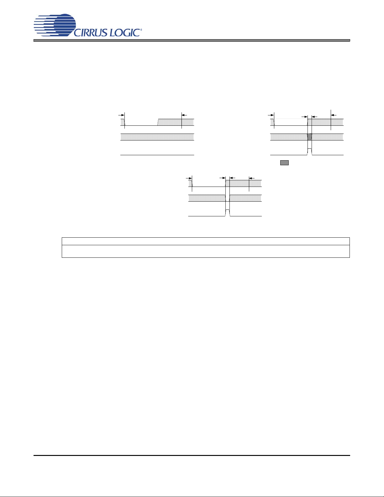
Figure 12. CLK_IN removed for > 2
Figure 13. CLK_IN removed for < 2
Figure 14. CLK_IN removed for < t
Figure 15. Low bandwidth and new clock domain .................................................................................... 18
Figure 16. High bandwidth with CLK_IN domain re-use ........................................................................... 18
Figure 17. Ratio Feature Summary ........................................................................................................... 20
Figure 18. PLL Clock Output Options ....................................................................................................... 21
Figure 19. Auxiliary Output Selection ........................... .......................................... ................................... 21
Figure 20. Control Port Timing in SPI Mode ............................................................................................. 23
Figure 21. Control Port Timing, I²C Write .................................................................................................. 24
Figure 22. Control Port Timing, I²C Aborted Write + Read .......................................................................24
23
SysClk cycles ................................................................................ 16
23
SysClk cycles but > t
CS .................................................................................................................................. 17
CS .................................................................................. 16
LIST OF TABLES
Table 1. Ratio Modifier .............................................................................................................................. 19
Table 2. Example 12.20 R-Values ............................................................................................................ 31
Table 3. Example 20.12 R-Values ............................................................................................................ 31
DS840F2 3
CS2100-CP
1
2
3
4
5
6
7
8
9
10
XTO
CLK_OUT
GND
VD
XTI/REF_CLK
AD0/CS
SCL/CCLK
SDA/CDIN
AUX_OUT
CLK_IN
1. PIN DESCRIPTION
Pin Name # Pin Description
VD 1 Digital Power (Input) - Positive power supply for the digital and analog sections.
GND 2 Ground (Input) - Ground reference.
CLK_OUT 3 PLL Clock Output (Output) - PLL clock output.
AUX_OUT
CLK_IN 5 Frequency Reference Clock Input (Input) - Clock input for the Digital PLL frequency reference.
XTO
XTI/REF_CLK
AD0/CS
SCL/CCLK
SDA/CDIN
4 Auxiliary Output (Output) - This pin outputs a buffered version of one of the input or output clocks,
or a status signal, depending on register configuration.
67Crystal Connections (XTI/XTO) / Timing Reference Clock Input (REF_CLK) (Input/Output) -
XTI/XTO are I/O pins for an external crystal which may be used to generate the low-jitter PLL input
clock. REF_CLK is an input for an externally generated low-jitter reference clock.
8 Address Bit 0 (I²C) / Control Port Chip Select (SPI) (Input) - AD0 is a chip address pin in I²C
Mode. CS is the chip select signal in SPI Mode.
9 Control Port Clock (Input) - SCL/CCLK is the serial clock for the serial control port in I²C and SPI
mode.
10 Serial Control Data (Input/Output) - SDA is the data I/O line in I²C Mode. CDIN is the input data
line for the control port interface in SPI Mode.
4 DS840F2
2. TYPICAL CONNECTION DIAGRAM
2
1
GND
SCL/CCLK
SDA/CDIN
2 kΩ
XTI/REF_CLK
Frequency Reference CLK_IN
XTO
CLK_OUT
AUX_OUT
0.1 µF
VD
+3.3 V
Notes:
1. Resistors
required for I
2
C
operation.
2 kΩ
AD0/CS
Low-Jitter
Timing Reference
System MicroController
1 µF
Note
1
1
or
2
REF_CLK
XTO
XTI
XTO
or
40 pF
x
40 pF
Crystal
To circuitry which requires
a low-jitter clock
N.C.
To other circuitry or
Microcontroller
Figure 1. Typical Connection Diagram
CS2100-CP
CS2100-CP
DS840F2 5
CS2100-CP
3. CHARACTERISTICS AND SPECIFICATIONS
RECOMMENDED OPERATING CONDITIONS
GND = 0 V; all voltages with respect to ground. (Note 1)
Parameters Symbol Min Typ Max Units
DC Power Supply VD 3.1 3.3 3.5 V
Ambient Operating Temperature (Power Applied)
Commercial Grade
Automotive Grade
T
AC
T
AD
-10
-40
-
-
+70
+85
°C
°C
Notes: 1. Device functionality is not guaranteed or implied outside of these limits. Operation outside of these limits
may adversely affect device reliability.
ABSOLUTE MAXIMUM RATINGS
GND = 0 V; all voltages with respect to ground.
Parameters Symbol Min Max Units
DC Power Supply VD -0.3 6.0 V
Input Current I
Digital Input Voltage (Note 2)V
Ambient Operating Temperature (Power Applied) T
Storage Temperature T
IN
IN
A
stg
-±10mA
-0.3 VD + 0.4 V
-55 125 °C
-65 150 °C
WARNING:Operation at or beyond these limits may result in permanent damage to the device.
Notes: 2. The maximum over/under voltage is limited by the input current except on the power supply pin.
DC ELECTRICAL CHARACTERISTICS
Test Conditions (unless otherwise specified): VD = 3.1 V to 3.5 V; TA = -10°C to +70°C (Commercial Grade);
T
= -40°C to +85°C (Automotive Grade).
A
Parameters Symbol Min Typ Max Units
Power Supply Current - Unloaded (Note 3)I
Power Dissipation - Unloaded (Note 3)P
Input Leakage Current I
Input Capacitance I
High-Level Input Voltage V
Low-Level Input Voltage V
High-Level Output Voltage (I
Low-Level Output Voltage (I
= -1.2 mA) V
OH
= 1.2 mA) V
OH
D
D
IN
C
IH
IL
OH
OL
Notes: 3. To calculate the additional current consumption due to loading (per output pin), multiply clock output
frequency by load capacitance and power supply voltage.
For example,
f
CLK_OUT
(49.152 MHz) * CL (15 pF) * VD (3.3 V) = 2.4 mA of additional current due to
these loading conditions on CLK_OUT.
-1218mA
-4060mW
--±10µA
-8-pF
70% - - VD
--30%VD
80% - - VD
--20%VD
6 DS840F2
CS2100-CP
AC ELECTRICAL CHARACTERISTICS
Test Conditions (unless otherwise specified): VD = 3.1 V to 3.5 V; TA = -10°C to +70°C (Commercial Grade);
= -40°C to +85°C (Automotive Grade); CL=15pF.
T
A
Parameters Symbol Conditions Min Typ Max Units
Crystal Frequency
Fundamental Mode XTAL
Reference Clock Input Frequency f
Reference Clock Input Duty Cycle D
Internal System Clock Frequency f
Clock Input Frequency f
Clock Input Pulse Width (Note 4)pw
Clock Skipping Timeout t
Clock Skipping Input Frequency f
PLL Clock Output Frequency f
PLL Clock Output Duty Cycle t
Clock Output Rise Time t
Clock Output Fall Time t
Period Jitter t
Base Band Jitter (100 Hz to 40 kHz) (Notes 7, 8) - 50 - ps rms
Wide Band JItter (100 Hz Corner) (Notes 7, 9) - 175 - ps rms
PLL Lock Time - CLK_IN (Note 10)t
PLL Lock Time - REF_CLK t
Output Frequency Synthesis Resolution (Note 11)f
f
XTAL
REF_CLK
REF_CLK
SYS_CLK
CLK_IN
CLK_IN
CS
CLK_SKIP
CLK_OUT
OD
OR
OF
JIT
LC
LR
err
RefClkDiv[1:0] = 10
RefClkDiv[1:0] = 01
RefClkDiv[1:0] = 00
RefClkDiv[1:0] = 10
RefClkDiv[1:0] = 01
RefClkDiv[1:0] = 00
8
16
32
8
16
32
-
18.75
-
37.5
-
-
-
-
50
18.75
37.5
75
MHz
MHz
MHz
MHz
MHz
MHz
45 - 55 %
8 18.75 MHz
50 Hz - 30 MHz
f
CLK_IN
f
CLK_IN
< f
> f
SYS_CLK
SYS_CLK
/96
/96
2
10
-
-
-
-
(Notes 5, 6)20--ms
(Note 6) 50 Hz - 80 kHz
6-75MHz
Measured at VD/2 45 50 55 %
20% to 80% of VD - 1.7 3.0 ns
80% to 20% of VD - 1.7 3.0 ns
(Note 7) - 70 - ps rms
f
< 200 kHz
CLK_IN
f
> 200 kHz
CLK_IN
f
REF_CLK
= 8 to 75 MHz - 1 3 ms
High Resolution
High Multiplication
-
100
-
1
0
0
200
3
-
±0.5
-
±112
ms
ppm
ppm
UI
ns
UI
Notes: 4. 1 UI (unit interval) corresponds to t
5. t
represents the time from the removal of CLK_IN by which CLK_IN must be re-applied to ensure that
CS
SYS_CLK
or 1/f
SYS_CLK
.
PLL_OUT continues while the PLL re-acquires lock. This timeout is based on the internal VCO frequency, with the minimum timeout occurring at the maximum VCO frequency. Lower VCO frequencies will
result in larger values of t
CS
.
6. Only valid in clock skipping mode; See “CLK_IN Skipping Mode” on page 14 for more information.
7.
f
CLK_OUT
= 24.576 MHz; Sample size = 10,000 points; AuxOutSrc[1:0] =11.
8. In accordance with AES-12id-2006 section 3.4.2. Measurements are Time Inte rval Error taken with 3rd
order 100 Hz to 40 kHz bandpass filter.
9. In accordance with AES-12id-2006 section 3.4.1. Measurements are Time Inte rval Error taken with 3rd
order 100 Hz Highpass filter.
10. 1 UI (unit inte rva l) co rr esponds to t
CLK_IN
or 1/f
CLK_IN
.
11. The frequency accuracy of the PLL clock output is directly proportional to the frequency accuracy of the
reference clock.
DS840F2 7
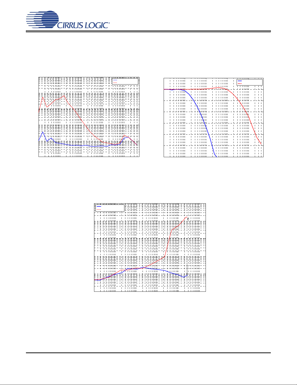
PLL PERFORMANCE PLOTS
1 10 100 1,000 10,000
0.1
1
10
100
1,000
10,000
Input Jitter Frequency (Hz)
Max Input Jitter Level (usec)
1 Hz Bandwidth
128 Hz Bandwidth
1 10 100 1000 10000
-60
-50
-40
-30
-20
-10
0
10
Input Jitter Frequency (Hz)
Jitter Transfer (dB)
1 Hz Bandwidth
128 Hz Bandwi dth
Figure 2. CLK_IN Sinusoidal Jitter Tolerance Figure 3. CLK_IN Sinusoidal Jitter Transfer
Samples size = 2.5M points; Base Band Jitter (10Hz to 40kHz). Samples size = 2.5M points; Base Band Jitter (10Hz to 40kHz).
Figure 4. CLK_IN Random Jitter Rejection and To lerance
0.01 0.1 1 10 100 1000
0.01
0.1
1
10
100
1000
Inpu t Jit ter Level ( nsec)
Output Jitt e r Level ( nsec)
1 Hz Bandwidt h
128 Hz Bandwidt h
Unlock
Unlock
Test Conditions (unless otherwise specified): VD = 3.3 V; TA=25°C; CL=15pF; f
CLK_IN
= 12.288 MHz; Sample size = 10,000 points; Base Band Jitter (100 Hz to 40 kHz); AuxOutSrc[1:0] =11.
f
CLK_OUT
CS2100-CP
= 12.288 MHz;
8 DS840F2
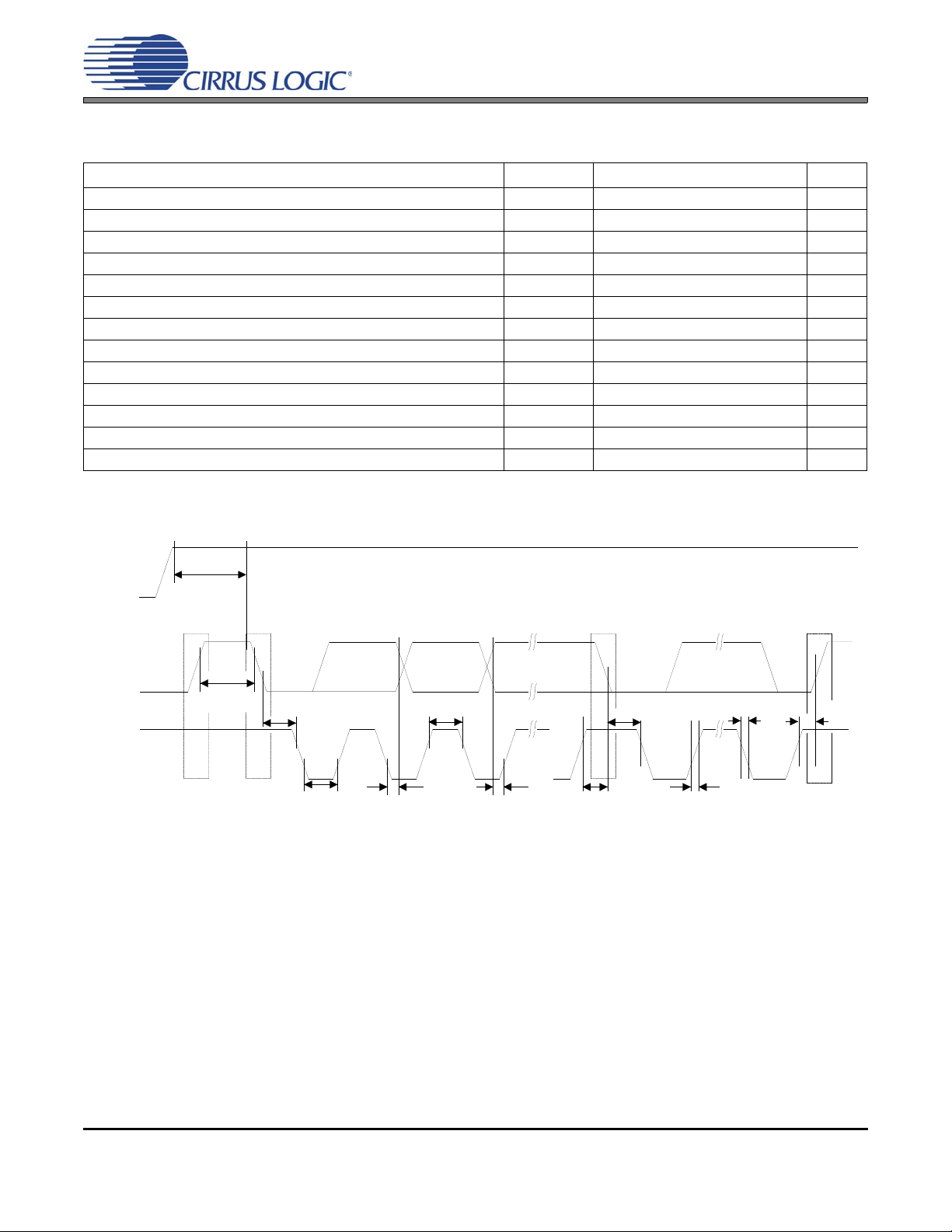
CONTROL PORT SWITCHING CHARACTERISTICS- I²C FORMAT
t
buf
t
hdst
t
hdst
t
low
t
r
t
f
t
hdd
t
high
t
sud
t
sust
t
susp
Stop
Start
Start
Stop
Repeated
SDA
SCL
VD
t
dpor
Figure 5. Control Port Timing - I²C Format
Inputs: Logic 0 = GND; Logic 1 = VD; CL=20pF.
Parameter Symbol Min Max Unit
SCL Clock Frequency f
Bus Free-Time Between Transmissions t
Start Condition Hold Time (prior to first clock pulse) t
Clock Low Time t
Clock High Time t
Setup Time for Repeated Start Condition t
SDA Hold Time from SCL Falling (Note 12)t
SDA Setup Time to SCL Rising t
Rise Time of SCL and SDA t
Fall Time SCL and SDA t
Setup Time for Stop Condition t
Acknowledge Delay from SCL Falling t
Delay from Supply Voltage Stable to Control Port Ready t
scl
buf
hdst
low
high
sust
hdd
sud
r
f
susp
ack
dpor
- 100 kHz
4.7 - µs
4.0 - µs
4.7 - µs
4.0 - µs
4.7 - µs
0-µs
250 - ns
-1µs
- 300 ns
4.7 - µs
300 1000 ns
100 - µs
CS2100-CP
Notes: 12. Data must be held for sufficient time to bridge the transition time, t
, of SCL.
f
DS840F2 9
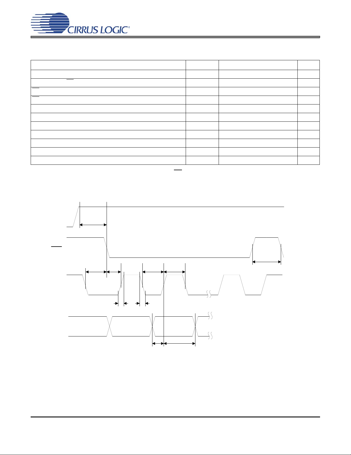
CONTROL PORT SWITCHING CHARACTERISTICS - SPI FORMAT
t
r2
t
f2
t
dsu
t
dh
t
sch
t
scl
CS
CCLK
CDIN
t
css
t
csh
t
spi
t
dpor
VD
Figure 6. Control Port Timing - SPI Format (Write Only)
Inputs: Logic 0 = GND; Logic 1 = VD; CL=20pF.
Parameter Symbol Min Max Unit
CCLK Clock Frequency f
CCLK Edge to CS
High Time Between Transmissions t
CS
Falling to CCLK Edge t
CS
CCLK Low Time t
CCLK High Time t
CDIN to CCLK Rising Setup Time t
CCLK Rising to DATA Hold Time (Note 14)t
Rise Time of CCLK and CDIN (Note 15)t
Fall Time of CCLK and CDIN (Note 15)t
Delay from Supply Voltage Stable to Control Port Ready t
Notes: 13.
Falling (Note 13)t
t
is only needed before first falling edge of CS after power is applied. t
spi
ccllk
spi
csh
css
scl
sch
dsu
dh
r2
f2
dpor
14. Data must be held for sufficient time to bridge the transition time of CCLK.
15. For f
< 1 MHz.
cclk
-6MHz
500 - ns
1.0 - µs
20 - ns
66 - ns
66 - ns
40 - ns
15 - ns
- 100 ns
- 100 ns
100 - µs
= 0 at all other times.
spi
CS2100-CP
10 DS840F2

4. ARCHITECTURE OVERVIEW
Fractional-N
Divider
Timing Reference
Clock
PLL Output
Voltage Controlled
Oscillator
Internal
Loop Filter
Phase
Comparator
N
Delta-Sigma
Modulator
4.1 Delta-Sigma Fractional-N Frequency Synthesizer
The core of the CS2100 is a Delta-Sigma Fractional-N Frequency Synthesizer which has very high-resolution for Input/Output clock ratios, low phase noise, very wide range of output frequencies and the ability to
quickly tune to a new frequency. In very simplistic terms, the Fractional-N Freq uency Synthesizer multiplies
the Timing Reference Clock by the value of N to generate the PLL out put clock. The desired output to input
clock ratio is the value of N that is applied to the delta-sigma modulator (see Figure 7).
The analog PLL based frequency synthesizer uses a low-jitter timing reference clock as a time and phase
reference for the internal voltage controlled oscillator (VCO). The phase comparator compares the fractional-N divided clock with the original timing reference and generates a control signal. The control signal is filtered by the internal loop filter to generate the VCO’s control voltage which sets its output frequency. The
delta-sigma modulator modulates the loop integer divide ratio to get the desired fractional ratio betwee n the
reference clock and the VCO output (thus the one’s density of the modulator sets the fractional value). This
allows the design to be optimized for very fast lock times for a wide rang e of outpu t freq uencies withou t the
need for external filter components. As with any Fractional-N Frequency Synthesizer the timing reference
clock should be stable and jitter-free.
CS2100-CP
4.2 Hybrid Analog-Digital Phase Locked Loop
DS840F2 11
Figure 7. Delta-Sigma Fractional-N Frequency Synthesizer
The addition of the Digital PLL and Fractional-N Logic (shown in Figure 8) to the Fractional-N Frequency
Synthesizer creates the Hybrid Analog-Digital Phase Locked Loop with many advantages over classical analog PLL techniques. These advantages include the ability to operate over extremely wide frequency ranges
without the need to change external loop filter components while maintaining impressive jitter reduction performance. In the Hybrid architecture, the Digital PLL calculates the ratio of the PLL output clock to the frequency reference and compares that to the desired ratio. The digital logic generates a value of N which is
then applied to the Fractional-N frequency synthesizer to generate the desired PLL outpu t frequency. Notice
that the frequency and phase of the timing reference signal do not affect the output of the PLL since the
digital control loop will correct for the PLL output. A major advantage of the Digital PLL is the ease with which
the loop filter bandwidth can be altered. The PLL bandwidth is autom atically set to a wide -band width mode
to quickly achieve lock and then reduced for optimal jitter rejection.

CS2100-CP
N
Digital Filter
Frequency
Comparator for
Frac-N Generation
Frequency Reference
Clock
Delta-Sigma Fractional-N Frequency Synthesizer
Digital PLL and Fractional-N Logic
Output to Input Ratio for Hybrid mode
Fractional-N
Divider
Timing Reference
Clock
PLL Output
Voltage Controlled
Oscillator
Internal
Loop Filter
Phase
Comparator
Delta-Sigma
Modulator
Figure 8. Hybrid Analog-Digital PLL
12 DS840F2

5. APPLICATIONS
Figure 9. Internal Timing Reference Clock Divider
N
Internal Timing
Reference Clock
PLL Output
Fractional-N
Frequency
Synthesizer
Timing Reference
Clock Divider
÷1
÷2
÷4
XTI/REF_CLK
RefClkDiv[1:0]
8 MHz < SysClk < 18.75 MHz
8 MHz < RefClk <
Timing Reference Clock
50 MHz (XTI)
75 MHz (REF_CLK)
-80 -60 -40 -20 0 20 40 60 80
20
40
60
80
100
120
140
160
180
Normalized REF__CLK Frequency (kHz)
Typical Base Band Jitter (psec)
CLK__OUT Jitt er
-15 kHz +15 kHz
CLK__OUT
f
*32/N
Figure 10. REF_CLK Frequency vs. a Fixed CLK_OUT
fLf
RefClkfH
≤≤
fLf
CLK_OUT
31
32
----- -
15kHz+×=
12.288MHz 0.96875 15kHz+×=
11.919MHz=
fHf
CLK_OUT
32
32
----- -
15kHz–×=
12.288MHz 115kHz+×=
12.273MHz=
5.1 Timing Reference Clock Input
The low jitter timing reference clock (RefClk) can be provided by either an external reference clock or an
external crystal in conjunction with the internal oscillator. In order to maintain a stable and low-jitter PLL output the timing reference clock must also be stable and low-jitter; the quality of the timing reference clock
directly affects the performance of the PLL and hence the quality of the PLL output.
5.1.1 Internal Timing Reference Clock Divider
The Internal Timing Reference Clock (SysClk) has a smaller maximum frequency th an what is allowed on
the XTI/REF_CLK pin. The CS2100 supports the wider external frequency range by offering an internal
divider for RefClk. The RefClkDiv[1:0] bits should be set such that SysClk, the divided RefClk, then falls
within the valid range as indicated in “AC Electrical Characteristics” on page 7.
CS2100-CP
It should be noted that the maximum allowable input frequency of the XTI/REF_CLK pin is dependent
upon its configuration as either a crystal connection or external clock input. See the “AC Electrical Char-
acteristics” on page 7 for more details.
For the lowest possible output jitter, attention should be paid to th e absolute frequency of the Timing Reference Clock relative to the PLL Output frequency ( CLK_OUT ). To minimize outp ut jitter, the Timing Reference Clock frequency should be chosen such that f
where N is an integer. Figure 10 shows the effect of varying the RefClk frequency around f
It should be noted that there will be a jitter null at the zero point when N = 32 (not shown in Figure 10). An
example of how to determine the range of RefClk frequencies around 12 MHz to be used in order to
achieve the lowest jitter PLL output at a frequency of 12.288 MHz is as follows:
where:
and
DS840F2 13
Referenced Control Register Location
RefClkDiv[1:0].......................“Reference Clock Input Divider (RefClkDiv[1:0])” on page 28
is at least +/-15 kHz from f
RefClk
CLK_OUT
CLK_OUT
*N/32
*N/32.

5.1.2 Crystal Connections (XTI and XTO)
XTI XTO
40 pF 40 pF
Figure 11. External Component Requirements for Crystal Circuit
An external crystal may be used to generate RefClk. To accomplish this, a 20 pF fundamental mode parallel resonant crystal must be connected between the XTI and XTO pins as shown in Figure 11. As shown,
nothing other than the crystal and its load capacitors should be connected to XTI and XTO. Please refer
to the “AC Electrical Characteristics” on page 7 for the allowed crystal frequency range.
5.1.3 External Reference Clock (REF_CLK)
For operation with an externally generated REF_CLK signal, XTI/REF_CLK should be connected to the
reference clock source and XTO should be left unconnected or pulled low through a 47 kΩ resistor to
GND.
CS2100-CP
5.2 Frequency Reference Clock Input, CLK_IN
The frequency reference clock input (CLK_IN) is used by the Digital PLL and Fractional-N Logic block to
dynamically generate a fractional-N value for the Frequency Synthesizer (see “Hybrid Ana log-Digital PL L”
on page 12). The Digital PLL first compares the CLK_IN frequency to the PLL output. The Fractional-N logic
block then translates the desired ratio based off of CLK_IN to one based off of the internal timing reference
clock (SysClk). This allows the low-jitter timing reference clock to be used as the clock which the Frequen cy
Synthesizer multiplies while maintaining synchronicity with the frequency reference clock through the Digital
PLL. The allowable frequency range for CLK_IN is found in the “AC Electrical Characteristics” on page 7.
5.2.1 CLK_IN Skipping Mode
CLK_IN skipping mode allows the PLL to maintain lock even when the CLK_IN signal has missing pulses
for up to 20 ms (t
skipping mode can only be used when the CLK_IN frequ ency is below 80 kHz and CLK_IN is reapplied
within 20 ms of being removed. The ClkSkipEn bit enables this function.
) at a time (see “AC Electrical Characteristics” on page 7 for specifications). CLK_IN
CS
14 DS840F2

CS2100-CP
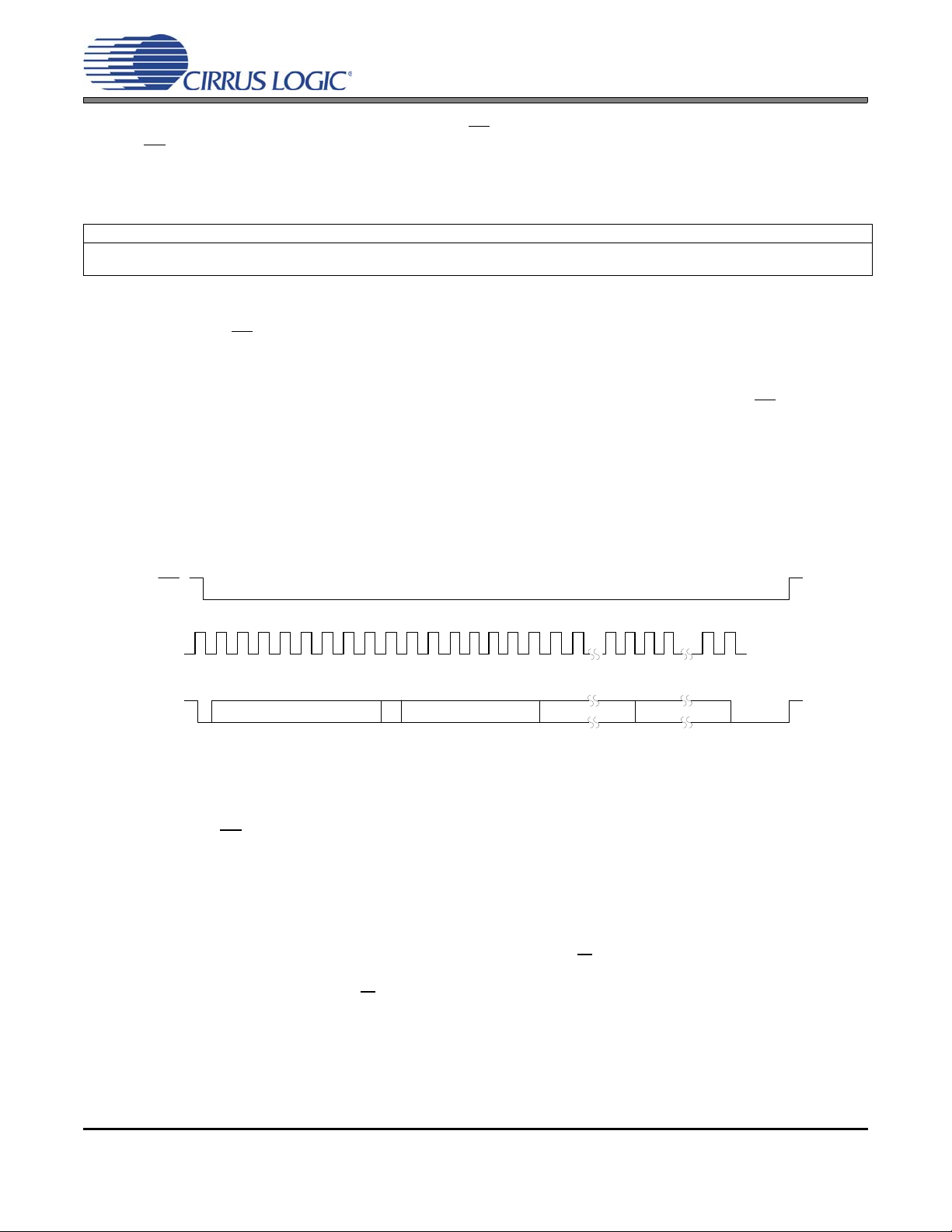
Figure 12. CLK_IN removed for > 223 SysClk cycles
CLK_IN
PLL_OUT
UNLOCK
ClkSkipEn=0 or 1
ClkOutUnl=0
Lock Time
CLK_IN
PLL_OUT
UNLOCK
ClkSkipEn=0 or 1
ClkOutUnl=1
Lock Time
= invalid clocks
223 SysClk cycles
2
23
SysClk cycles
CLK_IN
PLL_OUT
UNLOCK
ClkSkipEn=0 or 1
ClkOutUnl=0
Lock Time
CLK_IN
PLL_OUT
UNLOCK
ClkSkipEn=0 or 1
ClkOutUnl=1
Lock Time
t
CS
t
CS
= invalid clocks
CLK_IN
PLL_OUT
UNLOCK
ClkSkipEn= 1
ClkOutUnl= 0 or 1
Lock Time
t
CS
= invalid clocks
223 SysClk cycles
2
23
SysClk cycles
2
23
SysClk cycles
Figure 13. CLK_IN removed for < 223 SysClk cycles but > tCS
23
Regardless of the setting of the ClkSkipEn bit the PLL output will continue for 2
to 1048 ms) after CLK_IN is removed (see Figure 12). This is true as long as CLK_IN does not glitch or
have an effective change in period as the clock source is removed, otherwise the PLL will interpret this as
a change in frequency causing clock skipping and the 2
23
SysClk cycle time-out to be bypassed and the
PLL to immediately unlock. If the prior conditions are met while CLK_IN is r emoved and 2
pass, the PLL will unlock and the PLL_OUT state will be determined by the ClkOutUnl bit; See “PLL Clock
Output” on page 20. If CLK_IN is re-applied after such time, the PLL will remain unlocked for the specified
time listed in the “AC Electrical Characteristics” on page 7 after which lock will be acquired and the PLL
output will resume.
SysClk cycles (466 ms
23
SysClk cycles
If it is expected that CLK_IN will be removed and then reapplied within 2
t
, the ClkSkipEn bit should be disabled. If it is not disabled, the device will behave as shown in
CS
23
SysClk cycles but later than
Figure 13; note that the lower figure shows that the PLL output frequency may change and be incorrect
without an indication of an unlock condition.
DS840F2 15
CS2100-CP
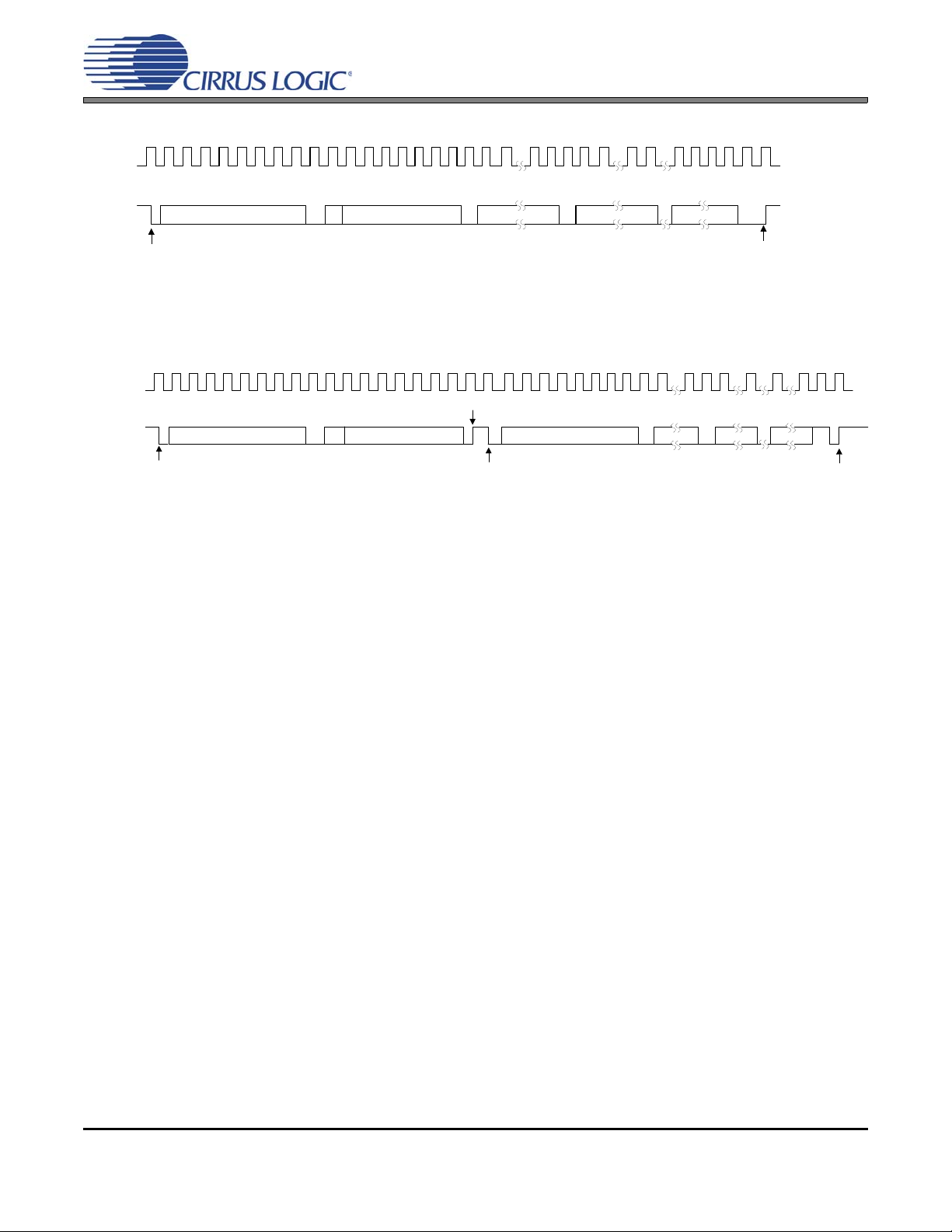
Figure 14. CLK_IN removed for < tCS
CLK_IN
PLL_OUT
UNLOCK
ClkSkipEn=1
ClkOutUnl=0 or 1
CLK_IN
PLL_OUT
UNLOCK
ClkSkipEn=0
ClkOutUnl=1
Lock Time
CLK_IN
PLL_OUT
UNLOCK
ClkSkipEn=0
ClkOutUnl=0
Lock Time
t
CS
t
CS
t
CS
= invalid clocks
If CLK_IN is removed and then re-applied within t
, the ClkSkipEn bit determines whether PLL_OUT
CS
continues while the PLL re-acquires lock (see Figure 14). When ClkSkipEn is disabled and CLK_IN is removed the PLL output will continue until CLK_IN is re-applied at which point the PLL will go unlocked only
for the time it takes to acquire lock; the PLL_OUT state will be determined by the ClkOutUnl bit during this
time. When ClkSkipEn is enabled and CLK_IN is removed the PLL output clock will remain continuous
throughout the missing CLK_IN period including the time while the PLL re-acquires lock.
Referenced Control Register Location
ClkSkipEn..............................“Clock Skip Enable (ClkSkipEn)” on page 28
ClkOutUnl..............................“Enable PLL Clock Output on Unlock (ClkOutUnl)” on page 29
5.2.2 Adjusting the Minimum Loop Bandwidth for CLK_IN
The CS2000 allows the minimum loop bandwidth of the Dig ital PLL to be adjusted betwe en 1 Hz and 12 8
Hz using the ClkIn_BW[2:0] bits. The minimum loop bandwidth of the Digital PLL directly affects the jitter
transfer function; specifically, jitter frequencies below the loop bandwidth corne r are passed from the PLL
input directly to the PLL output without attenuation. In some applications it is desirable to have a very low
minimum loop bandwidth to reject very low jitter frequencies, commonly referred to as wander. In others
it may be preferable to remove only higher frequency jitter, allowing the input wander to pass th rough th e
PLL without attenuation.
16 DS840F2
CS2100-CP
Figure 15. Low bandwidth and new clock domain
LRCK
SCLK
SDATA
MCLK
MCLK
Wander > 1 Hz
Wander and Jitter > 1 Hz Rejected
D0 D1
LRCK
SCLK
SDATA
Subclocks generated
from new clock domain.
or
PLL
BW = 1 Hz
CLK_IN
PLL_OUT
D0 D1
Jitter
Figure 16. High bandwidth with CLK_IN domain re-use
D0 D1
LRCK
SCLK
SDATA
MCLK
MCLK
Wander < 128 Hz
Jitter > 128 Hz Rejected
Wander < 128 Hz Passed to Output
LRCK
SCLK
SDATA
or
PLL
BW = 128 Hz
CLK_IN PLL_OUT
Subclocks and data re-used
from previous clock domain.
Jitter
D0 D1
Typically, applications in which the PLL_OUT signal creates a new clock do main from which all other system clocks and associated data are derived will benefit from the maximum jitter and wander rejection of
the lowest PLL bandwidth setting. See Figure 15.
Systems in which some clocks and data are derived from the PLL_OUT signal while other clocks and data
are derived from the CLK_IN signal will often require phase alignment of all the clocks and data in the
system. See Figure 16. If there is substantial wander on the CLK_IN signal in these applications, it may
be necessary to increase the minimum loop bandwidth allowing this wander to pass through to the
CLK_OUT signal in order to maintain phase alignment. Fo r these applications, it is advised to experim ent
with the loop bandwidth settings and choose the lowest bandwidth setting that does not produce system
timing errors due to wandering betw een the clocks and data synchronous to the CLK_IN domain and
those synchronous to the PLL_OUT domain .
It should be noted that manua l adjustment of the minimum loop bandwidth is not necessary to acquire
lock; this adjustment is made automatically by the Digital PLL. While acquiring lock, the digital loop bandwidth is automatically set to a large value. Once lock is achieved, the digital loop bandwidth will settle to
the minimum value selected by the ClkIn_BW[2:0] bits.
Referenced Control Register Location
ClkIn_BW[2:0].......................“Clock Input Bandwidth (ClkIn_BW[2:0])” on page 29
5.3 Output to Input Frequency Ratio Configuration
5.3.1 User Defined Ratio (R
The User Defined Ratio, RUD, is a 32-bit un-signed fixed-point number, stored in the Ratio register set,
which determines the basis for the desired input to output clock ratio. The 32-bit R
DS840F2 17
)
UD
can be expressed
UD

CS2100-CP
in either a high resolution (12.20) or high multiplication (20.12) format selectable by the LFRatioCfg bit,
with 20.12 being the default.
The R
for high resolution (12.20) format is encoded with 12 MSBs r eprese nting the integ er bin ary por-
UD
tion with the remaining 20 LSBs representing the fractional binary portion. The maximum multiplication
factor is approximately 4096 with a resolution of 0.954 PPM in this configuration. See “Calculating the
User Defined Ratio” on page 30 for more information.
The R
for high multiplication (20.12) format is encoded with 20 MSBs representing the integer binary
UD
portion with the remaining 12 LSBs representing the fractional binary portion. In this configuration, the
maximum multiplication factor is approximately 1,048,575 with a resolution of 244 PPM. It is recomme nded that the 12.20 High-Resolution format be utilized whenever the desired ratio is less than 4096 since
the output frequency accuracy of the PLL is directly proportional to the accuracy of the tim ing reference
clock and the resolution of the R
The status of internal dividers, such as the internal timing reference clock divider, are automatically taken
into account. Therefore R
Referenced Control Register Location
Ratio......................................“Ratio (Address 06h - 09h)” on page 27
LFRatioCfg............................“Low-Frequency Ratio Configuration (LFRatioCfg)” on page 29
UD
5.3.2 Ratio Modifier (R-Mod)
The Ratio Modifier is used to internally multiply/divide the RUD (the Ratio stored in the register space remains unchanged). The available options for R
.
UD
is simply the desired ratio of the output to input clock frequencies.
are summarized in Table 1 on page 18.
MOD
The R-Mod value selected by RModSel[2:0] is always used in the calculation for the Effective Ratio
(R
), see “Effective Ratio (REFF)” on page 19. If R-Mod is not desired, RModSel[2:0] should be left at
EFF
its default value of ‘000’, which corresponds to an R-Mod value of 1, thereby effectively disabling the ratio
modifier.
RModSel[2:0] Ratio Modifier
000
001
010
011
100
101
110
111
1
2
4
8
0.5
0.25
0.125
0.0625
Table 1. Ratio Modifier
Referenced Control Register Location
Ratio......................................“Ratio (Address 06h - 09h)” on page 27
RModSel[2:0] ........................“R-Mod Selection (RModSel[2:0])” section on page 26
18 DS840F2
CS2100-CP
Effective Ratio R
EFF
Ratio Format
Frequency Reference Clock
(CLK_IN)
SysClk
PLL Output
Frequency
Synthesizer
Digital PLL &
Fractional N Logic
N
Ratio
12.20
20.12
LFRatioCfg
RModSel[2:0]
Ratio
Modifier
R Correction
RefClkDiv[1:0]
Timing Reference Clock
(XTI/REF_CLK)
Divide
RefClkDiv[1:0]
User Defined Ratio R
UD
5.3.3 Effective Ratio (R
The Effective Ratio (R
previously described. R
R
= RUD • R
EFF
MOD
)
EFF
) is an internal calculation comprised of RUD and the appropriate modifiers, as
EFF
is calculated as follows:
EFF
To simplify operation the device handles some of the ratio calculation functions automatically (such as
when the internal timing reference clock divider is set). For this reason, the Effective Ratio does not need
to be altered to account for internal dividers.
Ratio modifiers which would produce an overflow or truncation of R
if R
is 1024 an R
UD
of 8 would produce an R
MOD
12.20 format. In all cases, the maximum and minimum allowable values for R
quency limits for both the input and output clocks as shown in the “AC Electrical Characteristics” on
page 7.
5.3.4 Ratio Configuration Summary
The RUD is the user defined ratio stored in the register space. The resolution for th e RUD is selectable by
setting LFRatioCfg. R-Mod is applied if selected. The user defined ratio, and ratio modifier make up the
effective ratio R
ratio is then corrected for the internal divid ers. The conceptual diagram in Figure 17 summarizes the fea-
tures involved in the calculation of the ratio va lues us ed to ge nerate the fractiona l-N value which con trols
the Frequency Synthesizer.
, the final calculation used to determine the output to input clock ratio. The effective
EFF
should not be used; For example
value of 8192 which exceeds the 4096 limit of the
EFF
EFF
are dictated by the fre-
EFF
DS840F2 19
Figure 17. Ratio Feature Summary
Referenced Control Register Location
Ratio......................................“Ratio (Address 06h - 09h)” on page 27
LFRatioCfg............................“Low-Frequency Ratio Configuration (LFRatioCfg)” on page 29
RModSel[2:0] ........................“R-Mod Selection (RModSel[2:0])” section on page 26
RefClkDiv[1:0].......................“Reference Clock Input Divider (RefClkDiv[1:0])” on page 28
5.4 PLL Clock Output
PLL Locked/Unlocked
PLL Output
2:1 Mux
ClkOutDis
2:1 Mux
ClkOutUnl
0
PLL Clock Output Pin
(CLK_OUT)
0
1
0
1
PLL Clock Output
PLLClkOut
Frequency Reference Clock
(CLK_IN)
PLL Lock/Unlock Indication
(Lock)
Timing Reference Clock
(RefClk)
PLL Clock Output
(PLLClkOut)
4:1 Mux
Auxiliary Output Pin
(AUX_OUT)
AuxOutDis
AuxOutSrc[1:0]
AuxLockCfg
The PLL clock output pin (CLK_OUT) provides a buffered version of the outp ut of the frequency synthesizer.
The driver can be set to high-impedance with the ClkOutDis bit.
The output from the PLL automatically drives a sta tic low condition while the PLL is un-locked (when the
clock may be unreliable). This feature can be disabled by setting the ClkOutUnl bit, however the state
CLK_OUT may then be unreliable during an unlock condition.
Referenced Control Register Location
ClkOutUnl..............................“Enable PLL Clock Output on Unlock (ClkOutUnl)” on page 29
ClkOutDis..............................“PLL Clock Output Disable (ClkOutDis)” on page 26
CS2100-CP
Figure 18. PLL Clock Output Options
5.5 Auxiliary Output
20 DS840F2
The auxiliary output pin (AUX_OUT) can be mapped, as shown in Figure 19, to one of four signals: reference clock (RefClk), input clock (CLK_IN), additional PLL clock output (CLK_OUT), or a PLL lock indicator
(Lock). The mux is controlled via the AuxOutSrc[1:0] bits. If AUX_OUT is set to Lock, the AuxLockCfg bit is
then used to control the output driver type and polarity of the LOCK signal (see section 8.6.2 on page 28).
If AUX_OUT is set to CLK_OUT the phase of the PLL Clock Output signal on AUX_OUT may differ from the
CLK_OUT pin. The driver for the pin can be set to high-impedance using the AuxOutDis bit.
Referenced Control Register Location
AuxOutSrc[1:0]......................“Auxiliary Output Source Selection (AuxOutSrc[1:0])” on page 26
AuxOutDis.............................“Auxiliary Output Disable (AuxOutDis)” on page 25
AuxLockCfg...........................“AUX PLL Lock Output Configuration (AuxLockCfg)” section on page 28
Figure 19. Auxiliary Output Selection

5.6 Clock Output Stability Considerations
5.6.1 Output Switching
CS2100 is designed such that re-configuration of the clock routing functions do not result in a partial clock
period on any of the active outputs (CLK_OUT and/or AUX_OUT). In particular, enabling or disabling an
output, changing the auxiliary output source between REF_CLK and CLK_OUT, and the automatic disabling of the output(s) during unlock will not cause a runt or partial clock period.
The following exceptions/limitations exist:
• Enabling/disabling AUX_OUT when AuxOutSrc[1:0] = 11 (unlock indicator).
• Switching AuxOutSrc[1:0] to or from 01 (PLL clock input) and to or from 11 (unlock indicator)
(Transitions between AuxOutSrc[1:0] = [00,10] will not produce a glitch).
• Changing the ClkOutUnl bit while the PLL is in operation.
When any of these exceptions occur, a partial clock period on the output may result.
5.6.2 PLL Unlock Conditions
Certain changes to the clock inputs and registers can cause the PLL to lose lock which will affect the presence the clock signal on CLK_OUT. The following outlines which conditions cause the PLL to go unlocked:
CS2100-CP
• Changes made to the registers which affect the Fraction-N value that is used by the Frequency Syn-
thesizer. This includes all the bits shown in Figure 17 on page 19.
• Any discontinuities on the Timing Reference Clock, REF_CLK.
• Discontinuities on the Frequency Reference Clock, CLK_IN, except when the Clock Skipping feature
is enabled and the requirements of Clock Skipping are satisfied (see “CLK_IN Skipping Mode” on
page 14).
• Gradual changes in CLK_IN frequency greater than ±30% from the starting frequency.
• Step changes in CLK_IN frequency.
5.7 Required Power Up Sequencing
• Apply power to the device. The output pins will remain low until the device is configured with a valid ratio
via the control port.
• Write the desired operational configurations. The EnDevCfg1 and EnDevCfg2 bits must be set to 1 dur-
ing the initialization register writes; the order does not matter.
– The Freeze bit may be set prior to this step and cleared afterward to ensure all settings take effect
at the same time.
6. SPI / I²C CONTROL PORT
The control port is used to access the registers and allows the device to be configured for the desired operational
modes and formats. The operation of the control port may be completely asynchronous with respect to device inpu ts
and outputs. However, to avoid potential interference problems, the control port pins should remain static if no operation is required.
DS840F2 21
CS2100-CP
4 5 6 7
CCLK
CHIP ADDRESS MAP BYTE DATA
1 0 0 1 1 1 1 0
CDIN
INCR 6 5 4 3 2 1 0 7 6 1 0
0 1 2 3 8 9 12 16 17 10 11 13 14 15
DATA +n
CS
7 6 1 0
Figure 20. Control Port Timing in SPI Mode
The control port operates wit h eith er t he SPI o r I²C inter face , with the CS 2100 ac ting a s a s lav e de vice. SPI Mo de
is selected if there is a high-to-low transition on the AD0/CS
the AD0/CS
pin through a resistor to VD or GND, thereby permanently selecting the desired AD0 bit address state.
In both modes the EnDevCfg1 and EnDevCfg2 bits must be set to 1 for normal operation.
WARNING:All “Reserved” registers must maintain their default state to ensure proper functional operation.
Referenced Control Register Location
EnDevCfg1............................“Enable Device Configuration Registers 1 (EnDevCfg1)” on page 27
EnDevCfg2............................“Enable Device Configuration Registers 2 (EnDevCfg2)” section on page 27
6.1 SPI Control
In SPI Mode, CS is the chip select signal; CCLK is the control port bit clock (sour ced from a microcontroller),
and CDIN is the input data line from the microcontroller. Data is clocked in on the rising edge of CCLK. The
device only supports write operations.
pin after power-up. I²C Mode is selected by connecting
Figure 20 shows the operation of the control port in SPI Mode. To write to a register, bring CS
eight bits on CDIN form the chip address and must be 10011110. The next eight bits form the Memory Address Pointer (MAP), which is set to the address of the register that is to be upd ated. The next eight bits ar e
the data which will be placed into the register designated by the MAP.
There is MAP auto increment capability, enabled by the INCR bit in the MAP register. If INCR is a zero, the
MAP will stay constant for successive read or writes. If INCR is set to a 1, the MAP will automatically increment after each byte is read or written, allowing block writes of successive registers.
6.2 I²C Control
In I²C Mode, SDA is a bidirectional data line. Data is clocked into and out of the device by the clock, SCL.
There is no CS
to VD or GND as appropriate. The stat e of the AD0 pin should be maintained throughout operation of the
device.
low. The first
pin. The AD0 pin forms the least-significant bit of the chip address and should be connected
The signal timings for a read and write cycle are sh own in Figure 21 and Figure 22. A Start condition is de-
fined as a falling transition of SDA while the clock is high. A Stop condition is a rising transition while the
clock is high. All other transitions of SDA occur while the clock is low. The first byte sent to the
a Start condition consists of the 7-bit chip address field and a R/W
bit (high for a read, low for a write). The
CS2100 after
upper 6 bits of the 7-bit address field are fixed at 100111 followed by the logic state of the AD0 pin. The
eighth bit of the address is the R/W
bit. If the operation is a write, the next byte is the Memory Address Pointer (MAP) which selects the register to be read or written. If the operation is a read, the contents of the register pointed to by the MAP will be output. Setting the auto increment bit in MAP allows successive reads or
writes of consecutive registers. Each byte is sepa rated by an acknowledge bit. The ACK bit is output from
the
CS2100 after each input byte is read and is input from the microcontroller after each transmitted byte.
22 DS840F2
CS2100-CP
4 5 6 7 24 25
SCL
CHIP ADDRESS (WRITE) MAP BYTE DATA
DATA +1
START
ACK
STOP
ACKACKACK
1 0 0 1 1 1 AD0 0
SDA
INCR 6 5 4 3 2 1 0 7 6 1 0 7 6 1 0 7 6 1 0
0 1 2 3 8 9 12 16 17 18 19 10 11 13 14 15 27 2826
DATA +n
Figure 21. Control Port Timing, I²C Write
SCL
CHIP ADDRESS (WRITE)
MAP BYTE
DATA
DATA +1
START
ACK
STOP
ACK
ACK
ACK
1 0 0 1 1 1 AD0 0
SDA
1 0 0 1 1 1 AD0 1
CHIP ADDRESS (READ)
START
INCR 6 5 4 3 2 1 0
7 0 7 0 7 0
NO
16 8 9 12 13 14 15 4 5 6 7 0 1 20 21 22 23 24
26 27 28
2 3 10 11 17 18 19 25
ACK
DATA + n
STOP
Figure 22. Control Port Timing, I²C Aborted Write + Read
Since the read operation cannot set the MAP, an aborted write operation is u sed a s a pr eamble. As sho wn
in Figure 21, the write operation is aborted after the acknowledge for the MAP byte by sending a stop condition. The following pseudocode illustrates an aborted write operation followed by a read operation.
Send start condition.
Send 100111x0 (chip address & write operation).
Receive acknowledge bit.
Send MAP byte, auto increment off.
Receive acknowledge bit.
Send stop condition, aborting write.
Send start condition.
Send 100111x1(chip address & read operation).
Receive acknowledge bit.
Receive byte, contents of selected register.
Send acknowledge bit.
Send stop condition.
Setting the auto increment bit in the MAP allows successive reads or writes of consecutive registers. Each
byte is separated by an acknowledge bit.
DS840F2 23

CS2100-CP
6.3 Memory Address Pointer
The Memory Address Pointer (MAP) byte comes after the address byte and selects the register to be read
or written. Refer to the pseudocode above for implementation details.
6.3.1 Map Auto Increment
The device has MAP auto increment capability enabled by the INCR bit (the MSB) of the MAP. If INCR is
set to 0, MAP will stay constant for successive I²C writes or reads and SPI writes. If INCR is set to 1, MAP
will auto increment after each byte is read or written, allowing block reads or writes of successive registers.
7. REGISTER QUICK REFERENCE
This table shows the register and bit names with their associated default values.
EnDevCfg1 and EnDevCfg2 bits must be set to 1 for normal operation.
WARNING:All “Reserved” registers must maintain their default state to ensure proper functional operation.
Adr Name 7 6 5 4 3 2 1 0
01h
Device ID Device4 Device3 Device2 Device1 Device0 Revision2 Revision1 Revision0
p25
02h
Device Ctrl Unlock Reserved Reserved Reserved Reserved Reserved AuxOutDis ClkOutDis
p25
03h
Device Cfg 1 RModSel2 RModSel1 RModSel0 Reser ved Reserved AuxOutSrc1 AuxOutSrc0 EnDevCfg1
p26
05h
Global Cfg Reserved Reserved Reserved Reserved Freeze Reserved Reserved EnDevCfg2
p27
06h
-
32-Bit Ratio
09h
16h
Funct Cfg 1 ClkSkipEn AuxLockCfg Reserved RefClkDiv1 RefClkDiv0 Reserved Reserved Reserved
p28
17h
Funct Cfg 2 Reserved Reserved Reserved ClkOutUnl LFRatioCfg Reserved Reserved Reserved
p29
1Eh
Funct Cfg 3 Reserved ClkIn_BW2 ClkIn_BW1 ClkIn_BW0 Reserved Reserved Reserved Reserved
p29
00000x xx
xxx00000
000000 00
000000 00
MSB ........................................................................................................................... MSB-7
MSB-8 ........................................................................................................................... MSB-15
LSB+15 ........................................................................................................................... LSB+8
LSB+7 ...........................................................................................................................LSB
000000 00
000000 00
000000 00
24 DS840F2
CS2100-CP
8. REGISTER DESCRIPTIONS
In I²C Mode all registers are read/write unless otherwise stated. In SPI mode all registers are write only. All “Reserved” registers must maintain their default state to ensure proper functional operation. The default state of each
bit after a power-up sequence or reset is indicated by the shaded row in the bit decode table and in the “Register
Quick Reference” on page 24.
Control port mode is entered when the device recognizes a valid chip address input on its I²C/SPI serial control pins
and the EnDevCfg1 and EnDevCfg2 bits are set to 1.
8.1 Device I.D. and Revision (Address 01h)
76543210
Device4 Device3 Device2 Device1 Device0 Revision2 Revision1 Revision0
8.1.1 Device Identification (Device[4:0]) - Read Only
I.D. code for the CS2100.
Device[4:0] Device
00000 CS2100.
8.1.2 Device Revision (Revision[2:0]) - Read Only
CS2100 revision level.
REVID[2:0] Revision Level
100 B2 and B3
110 C1
8.2 Device Control (Address 02h)
76543210
Unlock Reserved Reserved Reserved Reserved Reserved AuxOutDis ClkOutDis
8.2.1 Unlock Indicator (Unlock) - Read Only
Indicates the lock state of the PLL.
Unlock PLL Lock State
0 PLL is Locked.
1 PLL is Unlocked.
8.2.2 Auxiliary Output Disable (AuxOutDis)
This bit controls the output driver for the AUX_OUT pin.
AuxOutDis Output Driver State
0 AUX_OUT output driver enabled.
1 AUX_OUT output driver set to high-impedance.
Application: “Auxiliary Output” on page 20
DS840F2 25

CS2100-CP
8.2.3 PLL Clock Output Disable (ClkOutDis)
This bit controls the output driver for the CLK_OUT pin.
ClkOutDis Output Driver State
0 CLK_OUT output driver enabled.
1 CLK_OUT output driver set to high-impedance.
Application: “PLL Clock Output” on page 20
8.3 Device Configuration 1 (Address 03h)
76543210
RModSel2 RModSel1 RModSel0 Reserved Reserved AuxOutSrc1 AuxOutSrc0 EnDevCfg1
8.3.1 R-Mod Selection (RModSel[2:0])
Selects the R-Mod value, which is used as a factor in determining the PLL’s Fractional N.
RModSel[2:0] R-Mod Selection
000 Left-shift R-value by 0 (x 1).
001 Left-shift R-value by 1 (x 2).
010 Left-shift R-value by 2 (x 4).
011 Left-shift R-value by 3 (x 8).
100 Right-shift R-value by 1 (÷ 2).
101 Right-shift R-value by 2 (÷ 4).
110 Right-shift R-value by 3 (÷ 8).
111 Right-shift R-value by 4 (÷ 16).
Application: “Ratio Modifier (R-Mod)” on page 18
8.3.2 Auxiliary Output Source Selection (AuxOutSrc[1:0])
Selects the source of the AUX_OUT signal.
AuxOutSrc[1:0] Auxiliary Output Source
00 RefClk.
01 CLK_IN.
10 CLK_OUT.
11 PLL Lock Status Indicator.
Application: “Auxiliary Output” on page 20
Note: When set to 11, AuxLckCfg sets the polarity and driver type. See “AUX PLL Lock Output Config-
uration (AuxLockCfg)” on page 28.
26 DS840F2

CS2100-CP
8.3.3 Enable Device Configuration Registers 1 (EnDevCfg 1)
This bit, in conjunction with EnDevCfg2, configures the device for control port mode. These EnDevCfg
bits can be set in any order and at any time during the co ntrol por t acce ss seq uen ce, h owever they mu st
both be set before normal operation can occur.
EnDevCfg1 Register State
0 Disabled.
1 Enabled.
Application: “SPI / I²C Control Port” on page 21
Note: EnDevCfg2 must also be set to enable control port mode. See “SPI / I²C Control Port” on
page 21.
8.4 Global Configuration (Address 05h)
76543210
Reserved Reserved Reserved Reserved Freeze Reserved Reserved EnDevCfg2
8.4.1 Device Configuration Freeze (Freeze)
Setting this bit allows writes to the Device Control and Device Configuration registers (ad dress 02h - 04h)
but keeps them from taking effect until this bit is cleared.
FREEZE Device Control and Configuration Registers
0 Register changes take effect immediately.
1
Modifications may be made to Device Control and Device Configuration registers (registers 02h-04h) without
the changes taking effect until after the FREEZE bit is cleared.
8.4.2 Enable Device Configuration Registers 2 (EnDevCfg2)
This bit, in conjunction with EnDevCfg1, configures the device for control port mode. These EnDevCfg
bits can be set in any order and at any time during the co ntrol por t acce ss seq uen ce, h owever they mu st
both be set before normal operation can occur.
EnDevCfg2 Register State
0 Disabled.
1 Enabled.
Application: “SPI / I²C Control Port” on page 21
Note: EnDevCfg1 must also be set to enable control port mode. See “SPI / I²C Control Port” on
page 21.
8.5 Ratio (Address 06h - 09h)
76543210
MSB ............................................................................................................................ MSB-7
MSB-8 ............................................................................................................................ MSB-15
LSB+15 ............................................................................................................................ LSB+8
LSB+7 ............................................................................................................................ LSB
These registers contain the User Defined Ratio as shown in the “Register Quick Reference” section on
page 24. These 4 registers form a single 32-bit ratio value as shown above. See “Outp ut to Input Frequency
Ratio Configuration” on page 17 and “Calculating the User Defined Ratio” on page 30 for more details.
DS840F2 27

CS2100-CP
8.6 Function Configuration 1 (Address 16h)
76543210
ClkSkipEn AuxLockCfg Reserved RefClkDiv1 RefClkDiv0 Reserved Reserved Reserved
8.6.1 Clock Skip Enable (ClkSkipEn)
This bit enables clock skipping mode for the PLL and allows the PLL to maintain lock even when the
CLK_IN has missing pulses.
ClkSkipEn PLL Clock Skipping Mode
0 Disabled.
1 Enabled.
Application: “CLK_IN Skipping Mode” on page 14
Note: f
must be < 80 kHz an d re -a p plie d with in 20 ms to use this feature.
CLK_IN
8.6.2 AUX PLL Lock Output Configuration (AuxLockCfg)
When the AUX_OUT pin is configured as a lock indicator (AuxOutSrc[1:0] = 11), this bit configures the
AUX_OUT driver to either push-pull or open drain. It also determines the polarity of the lock signal. If
AUX_OUT is configured as a clock output, the state of this bit is disregarded.
AuxLockCfg AUX_OUT Driver Configuration
0 Push-Pull, Active High (output ‘high’ for unlocked condition, ‘low’ for locked condition).
1 Open Drain, Active Low (output ‘low’ for unlocked condition, high-Z for locked condition).
Application: “Auxiliary Output” on page 20
Note: AUX_OUT is an unlock indicator, signalling an error condition when the PLL is unlocked . There-
fore, the pin polarity is defined relative to the unlock condition.
8.6.3 Reference Clock Input Divider (RefClkDiv[1:0])
Selects the input divider for the timing reference clock.
RefClkDiv[1:0] Reference Clock Input Divider REF_CLK Frequency Range
00 ÷4. 32 MHz to 75 MHz (50 MHz with XTI)
01 ÷ 2. 16 MHz to 37.5 MHz
10 ÷ 1. 8 MHz to 18.75 MHz
11 Reserved.
Application: “Internal Timing Reference Clock Divider” on page 13
28 DS840F2

CS2100-CP
8.7 Function Configuration 2 (Address 17h)
76543210
Reserved Reserved Reserved ClkOutUnl LFRatioCfg Reserved Reserved Reserved
8.7.1 Enable PLL Clock Output on Unlock (ClkOutUnl)
Defines the state of the PLL output during the PLL unlock condition.
ClkOutUnl Clock Output Enable Status
0 Clock outputs are driven ‘low’ when PLL is unlocked.
1 Clock outputs are always enabled (results in unpredictable output when PLL is unlocked).
Application: “PLL Clock Output” on page 20
8.7.2 Low-Frequency Ratio Configuration (LFRatioCfg)
Determines how to interpret the 32-bit User Defined Ratio.
LFRatioCfg Ratio Bit Encoding Interpretation
0 20.12 - High Multiplier.
1 12.20 - High Accuracy.
Application: “User Defined Ratio (RUD)” on page 17
8.8 Function Configuration 3 (Address 1Eh)
76543210
Reserved ClkIn_BW2 ClkIn_BW1 ClkIn_BW0 Reserved Reserved Reserved Reserved
8.8.1 Clock Input Bandwidth (ClkIn_BW[2:0])
Sets the minimum loop bandwidth when locked to CLK_IN.
ClkIn_BW[2:0] Minimum Loop Bandwidth
000 1 Hz
001 2 Hz
010 4 Hz
011 8 Hz
100 16 Hz
101 32 Hz
110 64 Hz
111 128 Hz
Application: “Adjusting the Minimum Loop Bandwidth for CLK_IN” on page 16
Note: In order to guarantee that a change in minimum bandwidth takes effect, these bits must be set
prior to acquiring lock (removing and re-applying CLK_IN can provide the unlock condition necessary to
initiate the setting change). In production systems these bits should be configured with the desired values
prior to setting the EnDevCfg bits; this guarantees that the setting takes effect prior to acquiring lock.
DS840F2 29

CS2100-CP
9. CALCULATING THE USER DEFINED RATIO
Note: The software for use with the evaluation kit has built in tools to aid in calculating and converting the User
Defined Ratio. This section is for those who are not interested in the software or who are developing their
systems without the aid of the evaluation kit.
Most calculators do not interpr et the fixe d point bina ry representation which the CS2100 uses to define the output
to input clock ratio (see Section 5.3.1 on page 17); However, with a simple conversion we can use these tools to
generate a binary or hex value which can be written to the Ratio register.
9.1 High Resolution 12.20 Format
To calculate the User Defined Ratio (RUD) to store in the register(s), divide the desir ed output clock frequency by the given input clock (CLK_IN ). Then multiply the desired ratio by the scaling factor of 2
scaled decimal representation; then use the decimal to binary/hex conversion function on a calculator and
write to the register. A few examples have been provided in Table 2.
Desired Output to Input Clock Ratio
(output clock/input clock)
12.288 MHz/10 MHz=1.2288
11 .2896 MHz/44.1 kHz=256
Table 2. Example 12.20 R-Values
9.2 High Multiplication 20.12 Format
To calculate the User Defined Ratio (RUD) to store in the register(s), divide the desir ed output clock frequency by the given input clock (CLK_IN ). Then multiply the desired ratio by the scaling factor of 2
scaled decimal representation; then use the decimal to binary/hex conversion function on a calculator and
write to the register. A few examples have been provided in Table 3.
Desired Output to Input Clock Ratio
(output clock/input clock)
12.288 MHz/60 Hz=204,800
1 1.2896MHz/59.97 Hz =188254.127...
Scaled Decimal
Representation =
(output clock/input clock)
1288490 00 13 A9 2A
268435456 10 00 00 00
Scaled Decimal
Representation =
(output clock/input clock)
838860800 32 00 00 00
771088904 2D F5 E2 08
• 2
• 2
Hex Representation of
20
12
Binary R
Hex Representation of
Binary R
20
to get the
UD
12
to get the
UD
Table 3. Example 20.12 R-Values
30 DS840F2

10.PACKAGE DIMENSIONS
10L MSOP (3 mm BODY) PACKAGE DRAWING (Note 1)
E
N
1
23
e
b
A1
A2
A
D
SEATING
PLANE
E1
1
L
SIDE VIEW
END VIEW
TOP VIEW
∝
L1
c
INCHES MILLIMETERS NOTE
DIM MIN NOM MAX MIN NOM MAX
A -- -- 0.0433 -- -- 1.10
A1 0 -- 0.0059 0 -- 0.15
A2 0.0295 -- 0.0374 0.75 -- 0.95
b 0.0059 -- 0.0118 0.15 -- 0.30 4, 5
c 0.0031 -- 0.0091 0.08 -- 0.23
D -- 0.1181 BSC -- -- 3.00 BSC -- 2
E -- 0.1929 BSC -- -- 4.90 BSC --
E1 -- 0.1181 BSC -- -- 3.00 BSC -- 3
e -- 0.0197 BSC -- -- 0.50 BSC --
L 0.0157 0.0236 0.0315 0.40 0.60 0.80
L1 -- 0.0374 REF -- -- 0.95 REF --
CS2100-CP
Notes: 1. Reference document: JEDEC MO-187
2. D does not include mold flash or protrusions which is 0.15 mm max. per side.
3. E1 does not include inter-lead flash or protrusions which is 0.15 mm max per side.
4. Dimension b does not include a total allowable dambar protrusion of 0.08 mm max.
5. Exceptions to JEDEC dimension.
THERMAL CHARACTERISTICS
Parameter Symbol Min Typ Max Units
Junction to Ambient Thermal Impedance JEDEC 2-Layer
DS840F2 31
JEDEC 4-Layer
θ
JA
θ
JA
-
-
170
100
-
-
°C/W
°C/W
11.ORDERING INFORMATION
Contacting Cirrus Logic Support
For all product questions and inquiries, contact a Cirrus Logic Sales Representative.
To find one nearest you, go to www.cirrus.com
IMPORTANT NOTICE
Cirrus Logic, Inc. and its subsidiaries (“Cirrus”) believe that the information contained in this document is accurate and reliable. However, the information is subject
to change without noti ce and is provided “AS IS” wi thout war ranty of any kind (express or impli ed). Cust omers ar e advised t o obtain the latest version of relevant
information to verify, before placing orders, that information being relied on is current and complete. All products are sold subject to the terms and conditions of sale
supplied at the time of order acknowled gment, including tho se pertaining to warra nty, indemnification, an d limitation of liability. No responsibility is assumed by Cirrus
for the use of this information, including use of this information as the basis for manufacture or sale of any items, or for infringement of patents or other rights of third
parties. This document is the property of Cirrus and by furnishing this information, Cirrus grants no lice nse, express or implied under any patents, mask work rights,
copyrights, trademarks, trade secrets or other intellectual property rights. Cirrus owns the copyrights associated with the information contained herein and gives consent for copies to be made of the information only for use within your organization with respect to Cirrus integrated circuits or other products of Cirrus. This consent
does not extend to other copying such as copying for general distribution, advertising or promotional purposes, or for creating any work for resale.
CERTAIN APPLICATIONS USING SEMICONDUCTOR PRODUCTS MAY INVOLVE POTENTIAL RISKS OF DEATH, PERSONAL INJURY, OR SEVERE PROPERTY OR ENVIRONMENTAL DAMAGE (“CRITICAL APPLICATIONS”). CIRRUS PRODUCTS ARE NOT DESIGNED, AUTHORIZED OR WARRANTED FOR USE
IN PRODUCTS SURGICALLY IMPLANTED INTO THE BODY, AUTOMOTIVE SAFETY OR SECURITY DEVICES, LIFE SUPPORT PRODUCTS OR OTHER CRITICAL APPLICATIONS. INCLUSION OF CIRRUS PRODUCTS IN SUCH APPLICATIONS IS UNDERSTOOD TO BE FULLY AT THE CUSTOMER’S RISK AND CIRRUS DISCLAIMS AND MAKES NO WARRANTY, EXPRESS, STATUTORY OR IMPLIED, INCLUDING THE IMPLIED WARRANTIES OF MERCHANTABILITY AND
FITNESS FOR PARTICULAR PURPOSE, WITH REGARD TO ANY CIRRUS PRODUCT THAT IS USED IN SUCH A MANNER. IF THE CUSTOMER OR CUSTOMER’S CUSTOMER USES OR PERMITS THE USE OF CIRRUS PRODUCTS IN CRITICAL APPLICATIONS, CUSTOMER AGREES, BY SUCH USE, TO FULLY
INDEMNIFY CIRRUS, ITS OFFICERS, DI RECTORS, EMPL OYEES, DIST RIBUT ORS AND OTHER AGENTS FROM ANY AND ALL LIABILITY, INCLUDING ATTORNEYS’ FEES AND COSTS, THAT MAY RESULT FROM OR ARISE IN CONNECTION WITH THESE USES .
Cirrus Logic, Cirrus, and the Cirrus Logic logo designs are trade marks of Cirrus Logic, Inc. All other brand and product names in this document may be trademarks
or service marks of their respective owners.
I²C is a trademark of Philips Semiconductor.
SPI is a trademark of Motorola, Inc.
CS2100-CP
Product Description Package
CS2100-CP Clocking Device 10L-MSOP Yes
CS2100-CP Clocking Device 10L-MSOP Yes -10° to +70°C Tape and Reel CS2100CP-CZZR
CS2100-CP Clocking Device 10L-MSOP Yes
CS2100-CP Clocking Device 10L-MSOP Yes -40° to +85°C Tape and Reel CS2100CP-DZZR
Pb-Free Grade
Commercial
Automotive
Temp Range Container
-10° to +70°C Rail CS2100CP-CZZ
-40° to +85°C Rail CS2100CP-DZZ
Order#
CDK2000 Evaluation Platform - Yes - - - CDK2000-CLK
12.REFERENCES
1. Audio Engineering Society AES-12id-2006: “AES Information Document for digital audio measurements Jitter performance specifications,” May 2007.
2. Philips Semiconductor, “The I²C-Bus Specification: Version 2,” Dec. 1998.
http://www.semiconductors.philips.com
13.REVISION HISTORY
Release Changes
F1 Updated Pe riod Jitter specification in “AC Electrical Characteristics” on page 7.
Updated Crystal and Ref Clock Frequency specifications in “AC Electrical Characteristics” on page 7.
Added “PLL Performance Plots” section on page 8.
Updated “Internal Timing Reference Clock Divider” on page 13 and added Figure 10 on page 13.
Updated use conditions for “CLK_IN Skipping Mode” section on page 14 and page 28.
Updated Figure 12 on page 15.
Removed FsDetect and Auto R-Mod features per ER758rev2.
F2 Updated to add Automotive Grade temperature ranges and ordering options.
32 DS840F2
 Loading...