

Page 1
CS1615A
AC
Mains
BR1
BR1
BR1
BR 1
CS1615A/16A
FBAUX
GND
IAC
R2
GD
VDD
SOURCE
eOTP
NTC
16
13
5
14
R
S
Z1
FBSENSE
11
2
12
SGND4CTRL1 CTRL2
R
CTRL1RCTRL2
89
C1 C2
C3
C4
C5
V
rect
L1
Q1
V
AUX
R3 R4
R1
Q3
R
Sense
LED+
LED -
L2
R6
R7
D5
D4
C6
V
AUX
C7
D1
D3
D2
10
Q2
R5
CS1616A
Single Stage Dimmable Controller for LED Lamps
Features
• Reduced Off-chip BOM Compared to CS1615/16
• Best-in-class Dimmer Compatibility
- Leading-edge (TRIAC) Dimmers
- Trailing-edge Dimmers
- Digital Dimmers (Dimmers with an Integrated Power
Supply)
• Flicker-free Dimming
• 0% to 100% Smooth Dimming
• Optimized for Output Power <11W
• Primary-side Regulation (PSR)
• Active Power Factor Correction (PFC)
- >0.9 Power Factor
• Constant-current Output
- Flyback
- Buck-boost
• Tight LED Current Regulation: Better than ±5%
• Low THD: Less Than 20%
• Up to 90% Efficiency
• Fast Startup
• Meets NEMA SSL 6 Dimming Standard
- Closely Matches Incandescent S-curve
• Protection Features
- Output Open Circuit
- Output Short Circuit
- Overtemperature
Overview
The CS1615A and CS1616A are high-performance single
stage dimmable offline AC/DC controllers. The
CS1615A/16A requires fewer off-chip components than
the CS1615/16 resulting in a lower total BOM cost. The
CS1615A/16A provides unmatched single- and multi-lamp
dimmer-compatibility performance for dimmable LED
applications. The CS1615A is designed for 120VAC line
voltage applications, and the CS1616A is designed for
230VAC line voltage applications.
Across a broad range of dimmers, the CS1615A/16A
provides smooth flicker free dimming, and consistently
dims to nearly zero light output, which closely matches the
dimming performance of incandescent light bulbs. Cirrus
Logic’s patent pending approach to dimmer compatibility
provides full functionality on a wide range of dimmers,
including leading-edge, trailing-edge, and digital dimmers.
Applications
• Retro-fit LED Lamps
• External LED Drivers
• LED Luminaires
• Commercial Lighting
Ordering Information
See page 14.
Preliminary Product Information
Cirrus Logic, Inc.
http://www.cirrus.com
This document contains information for a product under development.
Cirrus Logic reserves the right to modify this product without notice.
Copyright Cirrus Logic, Inc. 2013
(All Rights Reserved)
AUG’13
DS1033PP2
Page 2
1. INTRODUCTION
2
IAC
SOURCE
5
SGND
15k
ADC
I
ref
11
FBSENSE
+
-
DAC
+
-
Peak
Contr ol
12
GND
OLP
+
-
OCP
Blank
3
CLAMP
V
OCP( th)
V
OLP(th)
V
Pk_Max(th)
I
CLAMP
+
-V
SOURCE(th)
MUX
9
+
-
I
CONNECT
V
CONNECT(th)
10
CTRL2
8
CTRL1
eOTP
FBAUX
16
+
-
Zer o-cur rent
Detect
+
-
Output
Over voltag e
V
ZCD(th)
V
OVP(th)
t
VAUX
14
VDD
+
-
V
DD(on)
V
DD(off)
Volt age
Regul ator
V
Z
POR
13
GD
VDD
VDD
VDD
4
+
V
FSTA RT(th )
3
CS1615A/16A
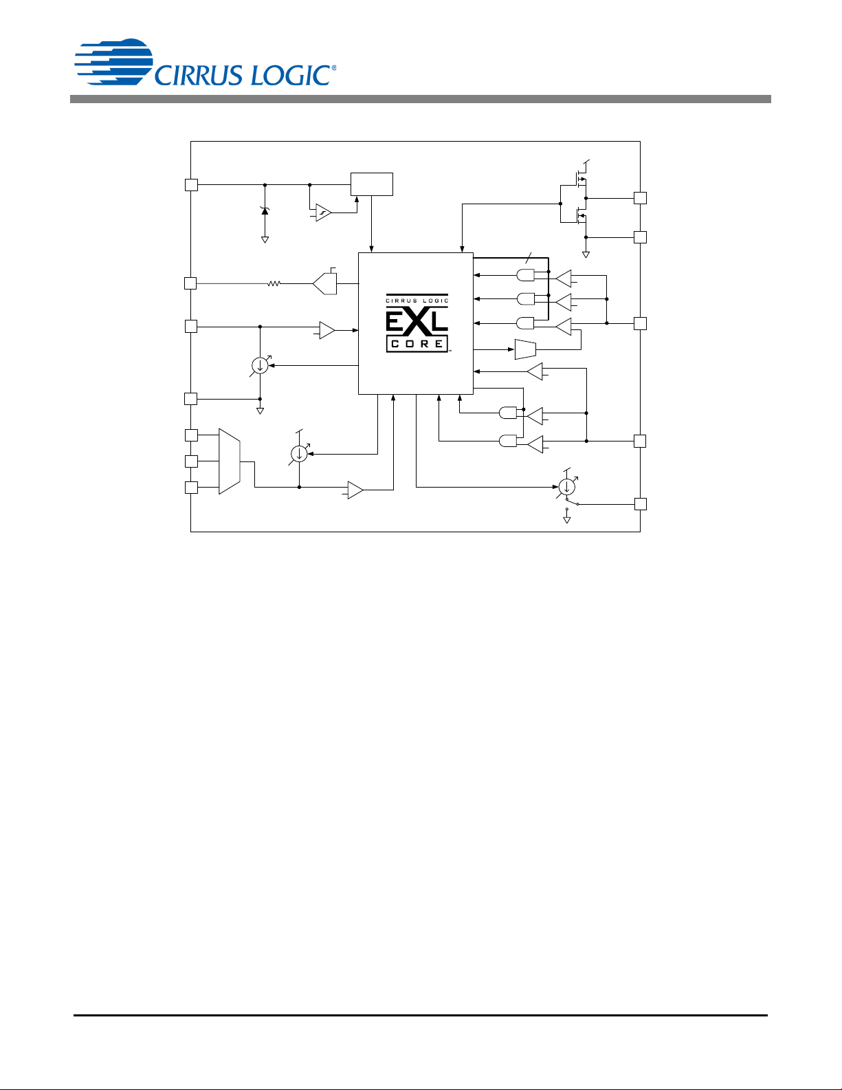
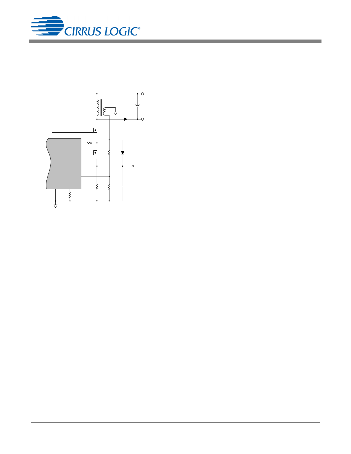
Figure 1. CS1615A/16A Block Diagram
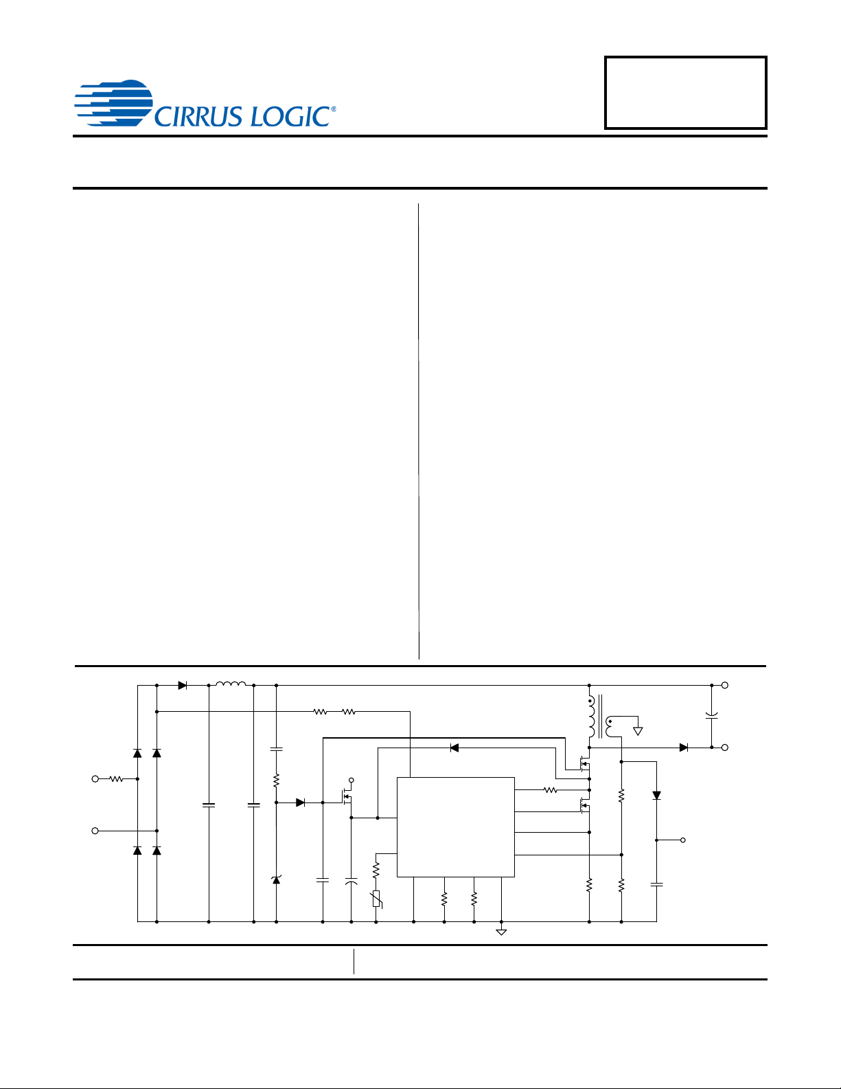
A typical schematic using the CS1615A/16A IC is shown on the
previous page.
Startup current is provided from a patent-pending, external, highvoltage source-follower network. In addition to providing startup
current, this unique topology is integral in providing compatibility
with digital dimmers by ensuring V
power is always available
DD
to the IC. During normal operation, an auxiliary winding on the
flyback transformer or buck-boost inductor back-biases the
source-follower circuit and provides steady-state operating
current to the IC to improve system efficiency.
Rectified input voltage V
and is used to control the adaptive dimmer-compatibility
is sensed as a current into pin IAC
rect
algorithm and to extract the phase of the input voltage for output
dimming control. The SOURCE pin is used to provide a control
signal for the high-voltage source-follower circuit during Leadingedge Mode and Trailing-edge Mode; it also provides the current
during startup.
2 DS1033PP2
The digital dual-mode controller is implemented with
peak-current mode primary-side regulation, which eliminates the
need for additional components to provide feedback from the
secondary and reduces system cost and complexity. Voltage
across a user-selected resistor is sensed through pin FBSENSE
to control the peak current of the primary-side inductor. Leadingedge and trailing-edge blanking on pin FBSENSE prevents false
triggering. The required target LED current and average flyback
transformer and buck-boost inductor input current are set by
attaching resistors R
CTRL2, respectively. The controller ensures half line-cycle
averaged constant output current.
Pin FBAUX is used for zero-current detection to ensure
quasi-resonant switching of the single stage output. When an
external negative temperature coefficient (NTC) thermistor is
connected to pin eOTP, the CS1615A/16A monitors the system
temperature, allowing the controller to reduce the output current
of the system. If the temperature reaches a designated high set
point, the IC is shut down and stops switching.
CTRL1
and R
on pins CTRL1 and
CTRL2
Page 3
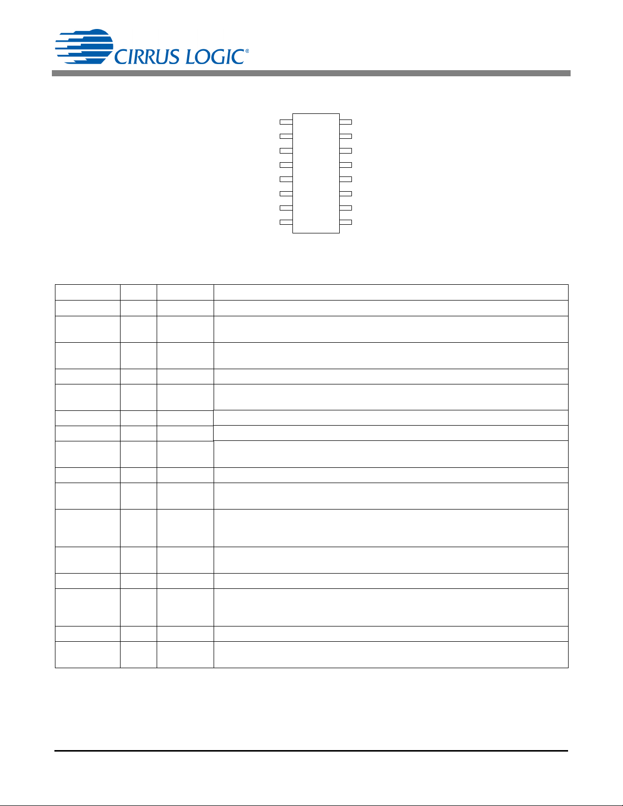
2. PIN DESCRIPTION
16 - l ead SOIC and TSSOP
16
Zero-current DetectFBAUX
15
No ConnectNC
14
IC Supply VoltageVDD
13
GD Gate Drive
10
eOTP External Overtem per atur e Protection
11
FBSENSE Fl yback C ur r ent Sense
12
GND Gr ound
9
LED Load Cur rentCTRL2
No Connect NC
1
2
IACRectifier Voltage Sense
3
Voltage Clamp Cur r ent Sour c e CLAMP
4
SGNDSource Gr ound
5
Source Switch SOURCE
6
NCNo Connect
7
No Connect NC
8
CTRL1Dimmer Hold Current
CS1615A/16A
Figure 2. CS1615A/16A Pin Assignments
Pin Name Pin # I/O
Description
NC 1INNo Connect — Leave pin unconnected.
IAC 2IN
CLAMP 3OUT
Rectifier Voltage Sense — A current proportional to the rectified line voltage is fed
into this pin. The current is measured with an A/D converter.
Voltage Clamp Current Source — Connect to a voltage clamp circuit on the sourceswitched dimmer-compatibility circuit.
SGND 4PWRSource Ground — Common reference current return for the SOURCE pin.
SOURCE 5IN
Source Switch — Connected to the source of the source-switched external high-volt-
age FET.
NC 6INNo Connect — Connect this pin to VDD using a 47k pull-up resistor.
NC 7INNo Connect — Connect this pin to VDD using a 47kpull-up resistor.
CTRL1 8IN
Dimmer Hold Current — Connect a resistor to this pin to set the minimum input cur-
rent being pulled by the flyback / buck-boost stage.
CTRL2 9INLED Load Current — Connect a resistor to this pin to set the LED current.
eOTP 10 IN
External Overtemperature Protection — Connect an external NTC thermistor to this
pin, allowing the internal A/D converter to sample the change to NTC resistance.
Feedback Current Sense — The current flowing in the power FET is sensed across a
FBSENSE 11 I N
resistor. The resulting voltage is applied to this pin and digitized for use by the computational logic to determine the FET's duty cycle.
GND 12 PWR
Ground — Common reference. Current return for both the input signal portion of the
IC and the gate driver.
GD 13 OUT Gate Drive — Gate drive for the power FET.
IC Supply Voltage — Connect a storage capacitor to this pin to serve as a reservoir
VDD 14 PWR
for operating current for the device, including the gate drive current to the power transistor.
NC 15 - No Connect — Leave pin unconnected.
FBAUX 16 IN
Zero-current Detect — Connect to the flyback/ buck-boost inductor auxiliary winding
for demagnetization current zero-crossing detection.
DS1033PP2 3
Page 4
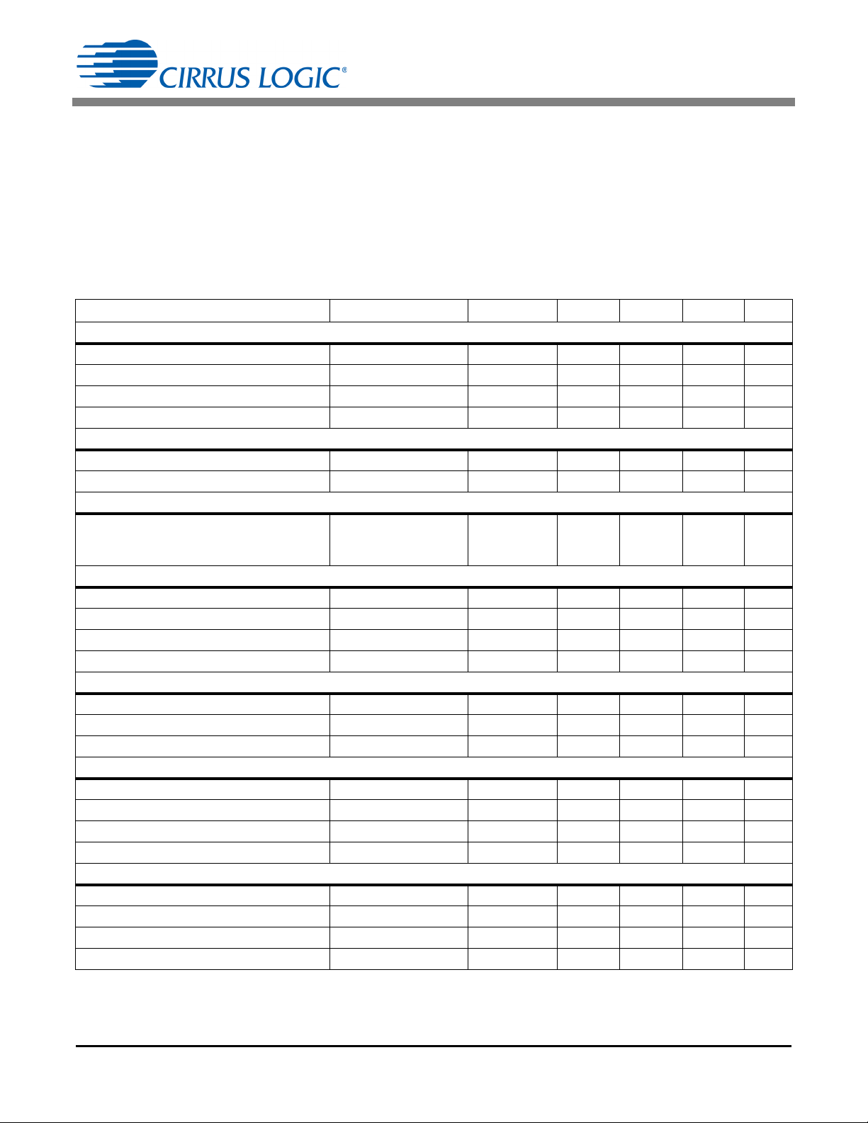
3. CHARACTERISTICS AND SPECIFICATIONS
3.1 Electrical Characteristics
CS1615A/16A
Typical characteristics conditions:
=25°C, VDD=12V, GND=0V
•T
A
• All voltages are measured with respect to GND.
Minimum/Maximum characteristics conditions:
•TJ= -40°C to +125 °C, VDD= 11V to 17 V, GND = 0 V
• Unless otherwise specified, all currents are positive
when flowing into the IC.
Parameter Condition Symbol Min Typ Max Unit
VDD Supply Voltage
Operating Range
Turn-on Threshold Voltage
Turn-off Threshold Voltage (UVLO)
Zener Voltage
(Note 1)
After Turn-on
VDD Increasing
VDD Decreasing
I
=20mA
DD
V
V
ST(th)
V
STP(th)
V
DD
11 - 17 V
-8.5-V
-7.5-V
Z
18.5 - 19.8 V
VDD Supply Current
Startup Supply Current
Operating Supply Current
(Note 2)
VDD<V
ST(th)
C
= 0.25nF, fsw70 kHz
L
I
ST
--200A
-4.5-mA
Reference
Reference Current
CS1615A
CS1616A
V
rect
rect
=200V
=400V
I
ref
-
-
133
133
-
-
A
A
V
Zero-current Detect
FBZCD Threshold V
FBZCD Blanking t
ZCD Sink Current
FBAUX Upper Voltage
(Note 3) I
I
=1mA
ZCD
FBZCD(th)
FBZCB
ZCD
-200-mV
-2-s
-2 - - mA
-VDD+0.6 - V
Current Sense
Max Peak Control Threshold V
Pk_Max(th)
Leading-edge Blanking t
LEB
-1.4-V
-550-ns
Delay to Output --100ns
Pulse Width Modulator
Minimum On Time - 0.55 - s
Maximum On Time - 12.8 - s
Minimum Switching Frequency t
Maximum Switching Frequency t
FB(Min)
FB(Max)
-6-kHz
-200-kHz
Gate Driver
Output Source Resistance Z
Output Sink Resistance Z
Rise Time
Fall Time
CL=0.25nF
CL=0.25nF
OUT
OUT
-24-
-11-
--30ns
--20ns
4 DS1033PP2
Page 5

CS1615A/16A
Parameter Condition Symbol Min Typ Max Unit
Flyback/Buck-boost Protections
Overcurrent Protection (OCP)
Overvoltage Protection (OVP)
Open Loop Protection (OLP)
(Note 4) V
(Note 5) V
(Note 4) V
OCP(th)
OVP(th)
OLP(th)
External Overtemperature Protection (eOTP)
Pull-up Current Source – Maximum I
Conductance Accuracy
Conductance Offset
(Note 6) --±5
(Note 6) -±250-nS
Current Source Voltage Threshold V
CONNECT
CONNECT(th)
Internal Overtemperature Protection (iOTP)
Thermal Shutdown Threshold
Thermal Shutdown Hysteresis
Notes: 1. The CS1615A/16A has an internal shunt regulator that limits the voltage on the VDD pin. Shunt regulation voltage VZ is defined
in the VDD Supply Voltage section on page 4.
2. For test purposes, load capacitance C
3. External circuitry should be designed to ensure that the ZCD current drawn from the internal clamp diode when it is forward biased
does not exceed specification.
4. Protection is implemented using pin FBSENSE. See the CS1615A/ 16A Block Diagram on page 2.
5. Protection is implemented using pin FBAUX. See the CS1615A/ 16A Block Diagram on page 2
6. The conductance is specified in Siemens (S or 1/ ). Each LSB of the internal ADC corresponds to 250nS or one parallel 4M
resistor. Full scale corresponds to 256 parallel 4M resistors or 15.625 k.
7. Specifications are guaranteed by design and are characterized and correlated using statistical process methods.
(Note 7) T
(Note 7) T
is connected to pin GD and is equal to 0.25nF.
L
SD
SD(Hy)
-1.69-V
-1.25-V
-200-mV
-80-A
-1.25-V
-135-ºC
-14-ºC
DS1033PP2 5
Page 6

CS1615A/16A
3.2 Thermal Resistance
Symbol Parameter SOIC TSSOP Unit
Junction-to-Ambient Thermal Impedance 2 Layer PCB
JA
Junction-to-Case Thermal Impedance 2 Layer PCB
JC
4 Layer PCB
4 Layer PCB
3.3 Absolute Maximum Ratings
Characteristics conditions:
All voltages are measured with respect to GND.
Pin Symbol Parameter Value Unit
14 V
1,2,8,9,
10,11,16
1,2,8,9,
10,11,16
13 V
13 I
5I
3I
SOURCE
CLAMP
-P
-T
-T
All Pins ESD
IC Supply Voltage 18.5 V
DD
Analog Input Maximum Voltage -0.5 to (V
Analog Input Maximum Current 5 mA
Gate Drive Output Voltage -0.3 to (VDD+0.3) V
GD
Gate Drive Output Current -1.0 / +0.5 A
GD
Current into Pin 1.1 A
Clamp Output Current 15 mA
Total Power Dissipation 400 mW
D
Junction Temperature Operating Range (Note 8) -40 to +125 °C
J
Storage Temperature Range -65 to +150 °C
Stg
Electrostatic Discharge Capability Human Body Model
Charged Device Model
119
105
50
44
138
103
44
28
DD
2000
500
+0.5) V
°C/W
°C/W
°C/W
°C/W
V
V
Note: 8. Long-term operation at the maximum junction temperature will result in reduced product life. Derate internal power dissipation at
the rate of 50 mW /°C for variation over temperature.
WARNING:
Operation at or beyond these limits may result in permanent damage to the device.
Normal operation is not guaranteed at these extremes.
6 DS1033PP2
Page 7
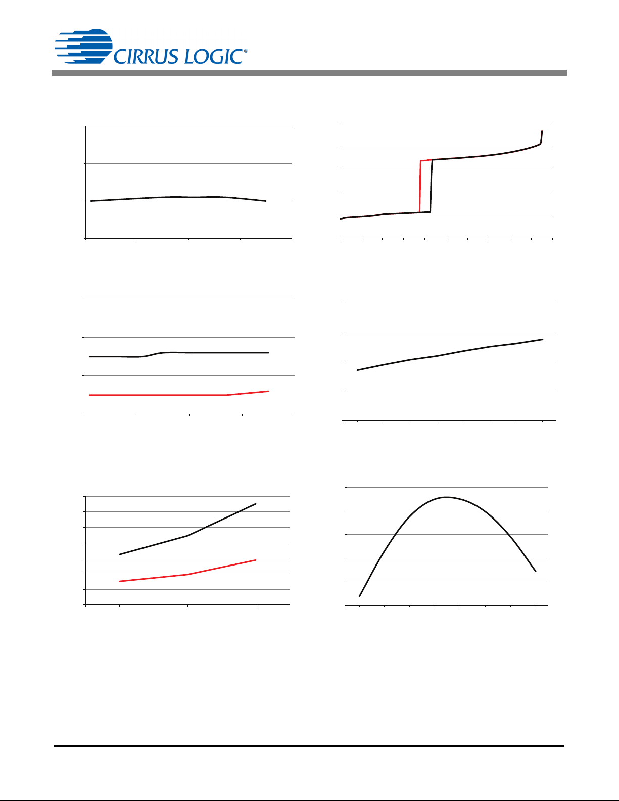
4. TYPICAL PERFORMANCE PLOTS
0
1
2
3
-50 0 50 100 150
UVLO Hysteresis
Temperature (ºC)
-2
0
2
4
6
8
02468101214161820
I
DD
(mA)
VDD(V)
Falling Edge
Rising Edge
7
8
9
10
-50 0 50 100 150
VDD (V)
Temperature (ºC)
Turn Off
Turn On
18
18.5
19
19.5
20
1251058555255-20-45
V
z
(V)
Temperature (ºC)
0
5
10
15
20
25
30
35
Resistance ()
Temperature (ºC)
Sink
Source
-43 25 125
-2.25
-1.75
-1.25
-0.75
-0.25
0.25
1251058555255-20-45
Drift (%)
CS1615A/16A
Figure 3. UVLO Characteristics
Figure 5. Turn On/ Off Threshold Voltage vs. Temperature
Figure 4. Supply Current vs. Voltage
Figure 6. Zener Voltage vs. Temperature
Figure 7. Gate Drive Resistance vs. Temperature
DS1033PP2 7
Temperature (°C)
Figure 8. Reference Current (I
) Drift vs. Temperature
ref
Page 8

CS1615A/16A
Figure 9. No-dimmer Mode Waveform
Figure 10. Leading-edge Mode Phase-cut Waveform
5. GENERAL DESCRIPTION
5.1 Overview
The CS1615A and CS1616A are high-performance single stage
dimmable offline AC/ DC controllers. The CS1615A /16A is a
cost-effective solution that provides unmatched single- and
multi-lamp dimmer-compatibility performance for dimmable LED
applications. The CS1615A is designed for 120VAC line voltage
applications, and the CS1616A is designed for 230VAC line
voltage applications.
Across a broad range of dimmers, the CS1615A /16A provides
smooth flicker free dimming, and consistently dims to nearly zero
light output, which closely matches the dimming performance of
incandescent light bulbs. Cirrus Logic’s patent pending approach
to dimmer compatibility provides full functionality on a wide range
of dimmers, including leading-edge, trailing-edge, and digital
dimmers.
5.2 IC Startup
A high-voltage source-follower circuit is used to deliver startup
current to the IC. During steady-state operation, an auxiliary
winding on the transformer/ inductor biases this circuit to an off
state to improve system efficiency, and all IC supply current is
provided from the auxiliary winding. The patent-pending
technology of the high-voltage source-follower circuit enables
system compatibility with digital dimmers (dimmers containing an
internal power supply) by providing a continuous path for the
dimmer’s power supply to recharge during its off state. During
steady-state operation, high-voltage FET Q2 in this circuit is
source-controlled by a variable internal current source on the
SOURCE pin to create the dimmer-compatibility circuit.
A resistor is connected between the SOURCE pin and the source
of source-follower FET. Resistor R5 is designed to control the
startup in-rush current into the SOURCE pin of the IC, which
allows for diode D3 to be specified as a standard low-cost diode.
During initial power-up, the IC executes a fast startup algorithm,
which drives the converter with peak currents that are above
normal to charge the output capacitor. Once the output capacitor
reaches a defined voltage, the IC drives the converter with
nominal peak currents until normal operation is achieved.
When the IC completes UVLO, it executes in Leading-edge
Mode until the dimmer switch detection algorithm determines the
appropriate operating mode for the IC. The dimmer switch
detection algorithm uses the input line voltage slope and dimmer
phase angle to determine the operating mode that matches the
type of dimmer switch in the system. From there on, it periodically
learns the dimmer type and can change the operating mode if the
type of dimmer switch changes.
5.3.1.1 No-dimmer Mode
If the CS1615A/ 16A determines that the line is not phase cut by
a dimmer switch, the IC operates the flyback/ buck-boost in PFC
mode to achieve a power factor greater than 0.9 while regulating
the load current to a level set by resistor R
No-dimmer Mode algorithm is applied to the source-controlled
dimmer-compatibility circuit for optimal performance, including
less than 20% of THD and highest possible overall efficiency.
. In addition, a
CTRL2
5.3.1.2 Leading-edge Mode
If the CS1615A/ 16A determines that the line is phase cut by a
leading-edge dimmer switch, the IC operates the flyback/buckboost in Dimmer Mode and the IC sets the dimmer firing current
as well as the attach current using a source-controlled dimmercompatibility circuit for stable TRIAC dimmer operation.
5.3 IC Operation
5.3.1 Dimmer Detection
The CS1615A/16A dimmer switch detection algorithm
determines if a non-dimming switch, a leading-edge dimmer
switch, or a trailing-edge dimmer switch controls the solid-state
lighting (SSL) system. For each type of switch, the IC uses a
different operating mode: for a non-dimming switch, No-dimmer
Mode is used; for a leading-edge dimmer switch, Leading-edge
Mode is used; for a trailing-edge dimmer switch, Trailing-edge
Mode is used. As a result, the overall performance is optimized
in terms of power losses, efficiency, power factor, THD, and
dimmer compatibility.
8 DS1033PP2
5.3.1.3 Trailing-edge Mode
If the CS1615A/16A determines that the line is phase cut by a
trailing-edge dimmer switch, the IC operates the flyback/buckboost in Dimmer Mode. The IC charges the capacitor in the
Page 9

CS1615A/16A
Figure 11. Trailing-edge Mode Phase-cut Waveform
CLAMP
R
Clamp
I
CLAMP
V
rect
S1
CS1615 A/16A
VDD
Q
CLAMP
T1
D
Snub
R
Snub
C
Snub
Q3
R
Sense
13
GD
2
SOURCE
Q2
3
R5
Figure 12. CLAMP Pin Model
R
CTRL2
CTRL2
FBAUX
GND
GD
912
CS1615A/16A
16
13
T1
D
Snub
R
Snub
C
Snub
Q3
R
Sense
V
rect
FBSENSE
11
C7
LED+
LED-
R6
C6
R7
V
AUX
D5
D4
Q2
SOURCE
5
R5
Figure 13. Flyback Model
dimmer switch on the falling edge of the input voltage using a
source-controlled dimmer-compatibility circuit.
5.3.2 Switch Overpower Protection
To prevent excessive power dissipation on the source-switched
FET Q2, the CS1615A/16A monitors voltage across FET Q2 and
current flow through FET Q2 to calculate average power
dissipation. If the calculated power exceeds the overpower
protection threshold, a fault condition occurs. The IC output is
disabled and the controller attempts to restart after
approximately thirty seconds.
5.4 Voltage Clamp Circuit
To keep trailing-edge dimmer switches conducting and from
misfiring, the dimmer switch internal capacitor has to be
charged quickly around the trailing edge of the phase-cut
waveform. In addition to the dimmer compatible circuit, an
optional clamp circuit provides a high-current sinking path for
delivering the required amount of charge onto the dimmer
switch capacitor in a short amount of time.
The CS1615A/16A provides active clamp circuitry on the
CLAMP pin, as shown in Figure 12.
5.4.1 Clamp Overpower Protection
The CS1615A/16A clamp overpower protection (COP) control
logic averages the turn-on time of the clamp circuit. If the output
of the averaging logic exceeds 10%, a COP event is actuated.
The clamp circuit is disabled as well as the flyback/ buck-boost
controller and the dimmer-compatibility circuit. The COP fault
state is not cleared until the power to the IC is recycled.
5.5 Dimmer Angle Extraction and the Dim Mapping Algorithm
When operating with a dimmer, the dimming signal is extracted
in the time domain and is proportional to the conduction angle of
the dimmer. A control variable is passed to the quasi-resonant
flyback/ buck-boost controller to achieve a wide range of output
currents.
5.6 Dual-mode Flyback /Buck-boost
The CS1615A/16A is configurable for isolated or non-isolated
topologies using a flyback transformer or buck-boost inductor,
respectively. The CS1615A/16A controls the dual-mode
flyback/ buck-boost to satisfy the dimmer hold current
requirement in Dimmer Mode and provide power factor
correction in No-dimmer Mode. The dual-mode ensures a
minimum average input current greater than the required dimmer
hold current when behind a dimmer and shapes the line current
when not behind a dimmer to provide power factor correction. It
also ensures half line-cycle averaged constant output current.
Figure 13 illustrates the dual-mode flyback topology. The
CS1615A/16A regulates output current using primary-side
control, which eliminates the need for opto-coupler feedback.
The control loop operates in peak current control mode.
Demagnetization time of the transformer is sensed by the
FBAUX pin using an auxiliary winding and is used as an input to
the control loop.
DS1033PP2 9
Page 10
CS1615A/16A
R
CTRL2
CTRL2
FBAU X
GND
GD
912
CS1615A/16A
16
13
Q3
R
Sense
V
rect
FBSEN SE
11
LED+
LED-
L2
R6
R7
D5
D4
C6
V
AUX
C7
Q2
R5
SOURCE
5
Figure 14. Buck-boost Model
R
CTRL2
1.4V N 4 M
1.25 511 R
SenseIOUT
----------------------------------------------------------------------- -
=
[Eq.1]
R
CTRL1
1.4V 4M
511 I
IN CCRSense
----------------------------------------------------------- -
=
[Eq.2]
I
PK max
1.4
R
Sense
------------------ -
=
[Eq.3]
Figure 14 illustrates the dual-mode buck-boost topology. The
CS1615A/16A regulates the output current by controlling the
peak current to ensure that the target output charge is achieved
every half line-cycle. Demagnetization time of the inductor is
sensed by the FBAUX pin using an auxiliary winding and is used
as an input to the control loop.
IC controls the inductor switching frequency and peak current to
ensure that the target output charge is achieved every half linecycle, thus regulating the output current.
5.6.3 Input Current Shaping
The CS1615A/16A shapes the input current by controlling the
peak primary current and the flyback/buck-boost switching
frequency. It shapes the currents differently when behind a
dimmer compared to when not behind a dimmer.
5.6.3.1 Operation Behind a Dimmer
Operating behind a dimmer, the CS1615A/16A controls the
switching frequency to ensure that the average input current is
greater than the dimmer hold current requirement. The dimmer
hold current level is sensed using resistor R
on pin CTRL1,
CTRL1
which is sampled periodically by an ADC. The value of this
resistor can be determined using the formula shown in
Equation 2.
where,
I
= constant input current used when designing circuit
IN(CC)
R
= resistor attached to pin FBSENSE
Sense
5.6.3.2 Operation in No-dimmer Mode
5.6.1 Primary-Side Current Control
All input current shaping and output power transfer is attained
using a peak current control algorithm. Demagnetization time of
the primary inductor is sensed by the FBAUX pin using an
auxiliary winding and is used as an input to the control algorithm.
The values obtained from R
CTRL1
and R
are the other
CTRL2
inputs to the control algorithm that help shape the input current
and control the LED current, respectively.
5.6.2 Output Current Regulation
The CS1615A/16A regulates output current by controlling the
charge transferred over a half line-cycle. The full-scale output
current target is set using resistor R
pin CTRL2. This pin is sampled periodically by an ADC. The
value of this resistor can be determined using Equation 1.
where,
N = turns ratio
I
= current through LED at maximum output
OUT
R
= resistor attached to pin FBSENSE
Sense
When designing a buck-boost topology, the turns ratio N is set to
one.
The CS1615A/16A uses the value obtained from resistor R
along with the phase-cut and line-cycle period information to
determine the corresponding target full-scale output charge. The
10 DS1033PP2
, which is connected on
CTRL2
CTRL2
Operating in No-dimmer Mode, the CS1615A/16A controls the
switching frequency to ensure that the average input current
follows the line voltage to provide power factor correction. In Nodimmer Mode the controller is designed to operate in quasiresonant mode to improve efficiency.
5.6.4 Max Primary-side Switching Current
Maximum primary-side switching current I
resistor R
connected to pin FBSENSE of the CS1615A/16.
Sense
The maximum primary-side switching current can be calculated
using Equation 3.
PK(max)
is set using
5.6.5 Auxiliary Winding Configuration
The auxiliary winding is used for zero-current detection (ZCD),
overvoltage protection (OVP), fast startup, and the steady-state
power supply. The voltage on the auxiliary winding is sensed
through pin FBAUX of the CS1615A/16A for zero-current
detection, overvoltage protection, and fast startup. The auxiliary
winding is also used to provide the steady-state power supply to
the CS1615A/16.
5.6.6 Output Open Circuit Protection
Output open circuit protection and output overvoltage protection
(OVP) are implemented by monitoring the output voltage through
the transformer auxiliary winding. If the voltage on the FBAUX pin
exceeds a threshold V
The IC output is disabled and the controller attempts to restart
after approximately one second.
of 1.25V, a fault condition occurs.
OVP(th)
Page 11

CS1615A/16A
CS1615A/16A
+
-
I
CONNECT
V
CONNECT
(th)
Com p_Out
eOTP
Control
eOTP
R
S
C
NTC
NTC
V
DD
10
(Optional)
Figure 15. eOTP Functional Diagram
Temperature (°C)
Cu rr e nt (I
LED
, Nom. )
125
95
50%
100%
0
25
Figure 16. eOTP Temperature vs. Impedance
5.6.7 Overcurrent Protection
Overcurrent protection (OCP) is implemented by monitoring the
voltage across the sense resistor. If this voltage exceeds a
threshold V
of 1.69V, a fault condition occurs. The IC
OCP(th)
output is disabled and the controller attempts to restart after
approximately one second.
5.6.8 Open Loop Protection
Open loop protection (OLP) and sense resistor short protection
are implemented by monitoring the voltage across the resistor. If
the voltage on pin FBSENSE does not reach the protection
threshold V
of 200mV, the IC output is disabled, and the
OLP(th)
controller attempts to restart after approximately one second.
5.7 Overtemperature Protection
The CS1615A/16A incorporates internal overtemperature
protection (iOTP) and the ability to connect an external
overtemperature sense circuit for IC protection. Typically, an
NTC thermistor is used.
5.7.1 Internal Overtemperature Protection
Internal overtemperature protection (iOTP) is activated, and
switching is disabled when the die temperature of the devices
exceeds 135°C. There is a hysteresis of about 14°C before
resuming normal operation.
5.7.2 External Overtemperature Protection
The external overtemperature protection (eOTP) pin is used to
implement overtemperature protection. A negative temperature
coefficient (NTC) thermistor resistive network is connected to pin
eOTP, usually in the form of a series combination of a resistor R
and a thermistor R
cyclically samples the resistance connected to pin eOTP.
(see Figure 15). The CS1615A/16A
NTC
scale down the internal dim level of the system (and hence LED
current I
) if the temperature exceeds 95 °C. The large time
LED
constant for this filter ensures that the dim scaling does not
happen spontaneously and is not noticeable (suppress spurious
glitches). The eOTP tracking circuit is designed to function
accurately with external capacitance up to 470pF.
The tracking range of this resistance ADC is approximately
15.5k to 4M. The series resistor R
is used to adjust the
S
resistance of the NTC to fall within the ADC tracking range,
allowing the entire dynamic range of the ADC to be well used.
The CS1615A/ 16A recognizes a resistance (R
S+RNTC
20.3k which corresponds to a temperature of 95°C, as the
beginning of an overtemperature dimming event and starts
reducing the power dissipation. The output current is scaled until
the series resistance (R
S+RNTC
) value reaches 16.6k (125°C).
Beyond this temperature, the IC shuts down until the resistance
(R
S+RNTC
) rises above 19.23k. This is not a latched protection
state, and the ADC keeps tracking the temperature in this state
in order to clear the fault state once the temperature drops below
110°C.
When exiting reset, the chip enters startup and the ADC quickly
(<5ms) tracks the external temperature to check if it is below the
110°C reference code before the controller is powered up. If this
check fails, the chip will wait until this condition becomes true
before initializing the rest of the system.
For example, a 14k (±1% tolerance) series resistor is required
to allow measurements of up to 130°C to be within the eOTP
tracking range when a 100k NTC with a Beta of 4275. If the
temperature exceeds 95°C, thermistor R
6.3k and series resistor R
S
resistance of 20.3k. The eOTP pin initiates protective dimming
is 14k, so the eOTP pin has a total
S
is approximately
NTC
action by reducing the power dissipation. At 125°C the thermistor
has 2.6k plus a series resistor RS equal to 14k present
R
NTC
a resistance of 16.6k at the eOTP pin reaching the point where
a thermal shutdown fault intervenes. The CS1615A /16A will
continue to monitor pin eOTP and once the series resistor R
plus the thermistor R
rises above 19.23k the device will
NTC
resume power conversion (see Figure 16).
) equal to
S
The total resistance on the eOTP pin gives an indication of the
temperature and is used in a digital feedback loop to adjust
current I
CONNECT
into the NTC and series resistor RS to maintain
a constant reference voltage V
I
CONNECT
is generated from a controlled current source with a
full-scale current of 80A. When the loop is in equilibrium, the
voltage on the eOTP pin fluctuates around V
resistance ADC is used to generate I
is filtered to suppress noise and compared against a reference
that corresponds to 125°C. A second low-pass filter with a time
constant of two seconds filters the ADC output and is used to
DS1033PP2 11
CONNECT(th)
CONNECT
of 1.25V. Current
CONNECT(th)
. A
. The ADC output
If the external overtemperature protection feature is not required,
connect the eOTP pin to GND using a 50k-to-500k resistor to
disable the eOTP feature.
Page 12
6. PACKAGE DRAWING
4&"5*/(1-"/&
1*/
*/%*$"503
& &
D
F
#
%
"
"
C
$
"
CCC $#"
%&5"*-"
5017*&8
4*%&7*&8
&/%7*&8
Y
EEE $ # "
Y5JQT
%&5"*-"
("6(&1-"/&
-
T
Y
BBB $
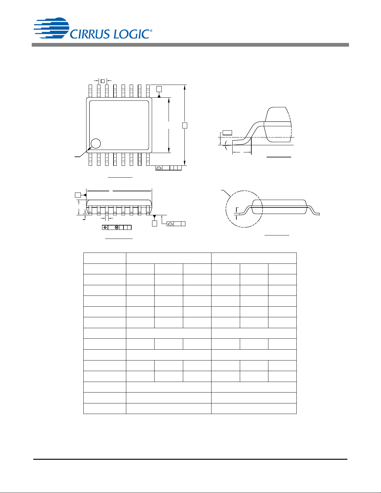
16-PIN TSSOP (173 MIL BODY)
CS1615A/16A
mm inch
Dimension MIN NOM MAX MIN NOM MAX
A - - - - 1.20 - - - - 0.047
A1 0.05 - - 0.15 0.002 - - 0.006
b 0.19 - - 0.30 0.007 - - 0.012
C 0.09 - - 0.20 0.004 - - 0.008
D 4.90 5.00 5.10 0.193 0.197 0.201
E 6.40 BSC 0.252 BSC
E1 4.30 4.40 4.50 0.169 0.173 0.177
e 0.65 BSC 0.026 BSC
L 0.45 0.60 0.75 0.018 0.024 0.030
Θ 0°- -8°0°- -8°
aaa 0.10 0.004
bbb 0.10 0.004
ddd 0.20 0.008
1. Controlling dimensions are in millimeters.
2. Dimensioning and tolerances per ASME Y14.5 M.
3. This drawing conforms to JEDEC outline MO-153, variation AB.
4. Recommended reflow profile is per JEDEC/IPC J-STD-020.
12 DS1033PP2
Page 13
CS1615A/16A
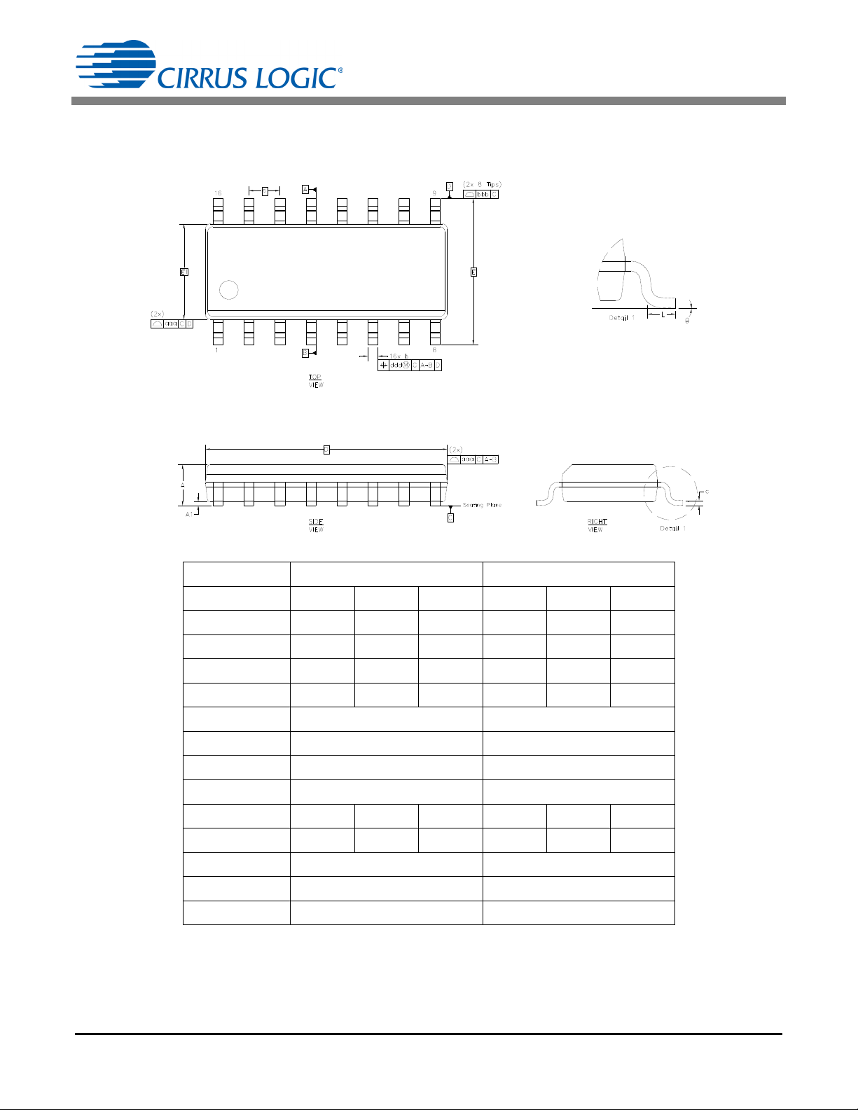
16-PIN SOICN (150 MIL BODY)
Dimension MIN NOM MAX MIN NOM MAX
A - - - - 1.75 - - - - 0.069
A1 0.10 - - 0.25 0.004 - - 0.010
b 0.31 - - 0.51 0.012 - - 0.020
c 0.10 - - 0.25 0.004 - - 0.010
D 9.90 BSC 0.390 BSC
E 6.00 BSC 0.236 BSC
E1 3.90 BSC 0.154 BSC
e 1.27 BSC 0.050 BSC
L 0.40 - - 1.27 0.016 - - 0.050
Θ 0°- -8°0°- -8°
aaa 0.10 0.004
bbb 0.25 0.010
ddd 0.25 0.010
Notes: 1. Controlling dimensions are in millimeters.
2. Dimensions and tolerances per ASME Y14.5 M.
3. This drawing conforms to JEDEC outline MS-012, variation AC for standard 16 SOICN narrow body.
4. Recommended reflow profile is per JEDEC/IPC J-STD-020.
mm inch
DS1033PP2 13
Page 14

CS1615A/16A
7. ORDERING INFORMATION
Ordering Number Container AC Line Voltage Temperature Package
CS1615A-FSZ Bulk
CS1615A-FSZR Tape & Reel
CS1616A-FSZ Bulk
CS1616A-FSZR Tape & Reel
CS1615A-FZZ Bulk
CS1615A-FZZR Tape & Reel
CS1616A-FZZ Bulk
CS1616A-FZZR Tape & Reel
120VAC -40 °C to +125 °C 16-lead SOICN, Lead (Pb) Free
230VAC -40 °C to +125 °C 16-lead SOICN, Lead (Pb) Free
120VAC -40 °C to +125 °C 16-lead TSSOP, Lead (Pb) Free
230VAC -40 °C to +125 °C 16-lead TSSOP, Lead (Pb) Free
8. ENVIRONMENTAL, MANUFACTURING, & HANDLING INFORMATION
Part Number Peak Reflow Temp MSL Rating
CS1615A-FSZ 260 °C 3 7 Days
CS1616A-FSZ 260 °C 3 7 Days
CS1615A-FZZ 260 °C 3 7 Days
CS1616A-FZZ 260 °C 3 7 Days
a
Max Floor Life
b
a.MSL (Moisture Sensitivity Level) as specified by IPC/JEDEC J-STD-020.
b.Stored at 30°C, 60% relative humidity.
14 DS1033PP2
Page 15

REVISION HISTORY
Revision Date Changes
PP1 JUL 2013 Edited content to move source switcher
PP2 AUG 2013 Context clarification
CS1615A/16A
DS1033PP2 15
Page 16

CS1615A/16A
Contacting Cirrus Logic Support
For all product questions and inquiries contact a Cirrus Logic Sales Representative. To find the one nearest to you
go to www.cirrus.com
IMPORTANT NOTICE
"Preliminary” product information describes products that are in production, but for which full characterization data is not yet available.
Cirrus Logic, Inc. and its subsidiaries ("Cirrus") believe that the information contained in this document is accurate and reliable. However, the information is subject
to change without notice and is provided "AS IS" without warranty of any kind (express or implied). Customers are advised to obtain the latest version of relevant
information to verify, before placing orders, that information being relied on is current and complete. All products are sold subject to the terms and conditions of sale
supplied at the time of order acknowledgment, including those pertaining to warranty, indemnification, and limitation of liability. No responsibility is assumed by Cirrus
for the use of this information, including use of this information as the basis for manufacture or sale of any items, or for infringement of patents or other rights of third
parties. This document is the property of Cirrus and by furnishing this information, Cirrus grants no license, express or implied under any patents, mask work rights,
copyrights, trademarks, trade secrets or other intellectual property rights. Cirrus owns the copyrights associated with the information contained herein and gives
consent for copies to be made of the information only for use within your organization with respect to Cirrus integrated circuits or other products of Cirrus. This consent does not extend to other copying such as copying for general distribution, advertising or promotional purposes, or for creating any work for resale.
CERTAIN APPLICATIONS USING SEMICONDUCTOR PRODUCTS MAY INVOLVE POTENTIAL RISKS OF DEATH, PERSONAL INJURY, OR SEVERE PROPERTY OR ENVIRONMENTAL DAMAGE ("CRITICAL APPLICATIONS"). CIRRUS PRODUCTS ARE NOT DESIGNED, AUTHORIZED OR WARRANTED FOR
USE IN PRODUCTS SURGICALLY IMPLANTED INTO THE BODY, AUTOMOTIVE SAFETY OR SECURITY DEVICES, LIFE SUPPORT PRODUCTS OR OTHER
CRITICAL APPLICATIONS. INCLUSION OF CIRRUS PRODUCTS IN SUCH APPLICATIONS IS UNDERSTOOD TO BE FULLY AT THE CUSTOMER'S RISK
AND CIRRUS DISCLAIMS AND MAKES NO WARRANTY, EXPRESS, STATUTORY OR IMPLIED, INCLUDING THE IMPLIED WARRANTIES OF MERCHANTABILITY AND FITNESS FOR PARTICULAR PURPOSE, WITH REGARD TO ANY CIRRUS PRODUCT THAT IS USED IN SUCH A MANNER. IF THE CUSTOMER
OR CUSTOMER'S CUSTOMER USES OR PERMITS THE USE OF CIRRUS PRODUCTS IN CRITICAL APPLICATIONS, CUSTOMER AGREES, BY SUCH USE,
TO FULLY INDEMNIFY CIRRUS, ITS OFFICERS, DIRECTORS, EMPLOYEES, DISTRIBUTORS AND OTHER AGENTS FROM ANY AND ALL LIABILITY, INCLUDING ATTORNEYS' FEES AND COSTS, THAT MAY RESULT FROM OR ARISE IN CONNECTION WITH THESE USES.
Use of the formulas, equations, calculations, graphs, and/or other design guide information is at your sole discretion and does not guarantee any specific results or
performance. The formulas, equations, graphs, and/or other design guide information are provided as a reference guide only and are intended to assist but not to
be solely relied upon for design work, design calculations, or other purposes. Cirrus Logic makes no representations or warranties concerning the formulas, equations, graphs, and/or other design guide information.
Cirrus Logic, Cirrus, the Cirrus Logic logo designs, EXL Core, and the EXL Core logo design are trademarks of Cirrus Logic, Inc. All other brand and product names
in this document may be trademarks or service marks of their respective owners.
16 DS1033PP2
 Loading...