

Page 1
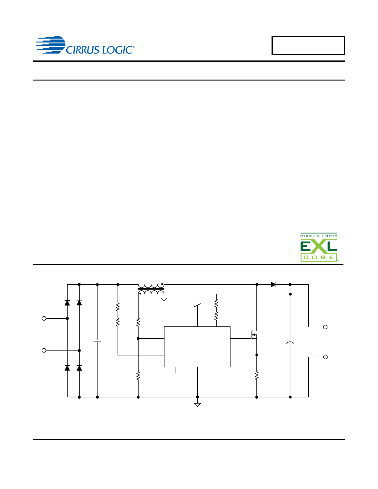
CS1501
R1
R2 R3
R4 R7
R5
R6
8 1
D1
C1 C2
Regulated
DC Output
Q1
AC
Mains
BR 1
BR 1
BR 1
BR1
CS1501
GDZCD
IFB
GND
CSIAC
VD D
L
B
6
3
57
4
V
DD
STB Y
2
V
link
V
rect
Digital Power Factor Correction Control IC
Features
Digital EMI Noise Shaping
Adaptive Digital Energy Controller
• Excellent Efficiency Under All Load and Line Conditions
• Zero-voltage Switching Topology
Minimal External Devices Required
Adaptive Digital Control Loop
Comprehensive Safety Features
• Undervoltage Lockout (UVLO)
• Output Overvoltage Protection
• Cycle-by-cycle Current Limiting
• Open/Short Loop Protection for IAC & IFB Pins
• Thermal Shutdown
Pin Placement Similar to Traditional Boundary Mode (CRM)
Controllers
Applications
LCD and LED TVs
Notebooks
Server/Telecom
Overview
The CS1501 is a high-performance digital power factor
correction (PFC) controller designed for switching mode power
supply (SMPS) applications. The CS1501 actively manages
the power factor correction while achieving high efficiency over
a wide load range.
The CS1501 adaptively controls the input AC current so that it
is in phase with the AC mains voltage, and its waveform mimics
the input voltage waveform. The PFC controller executes
adaptive digital algorithms designed to shape the AC mains
input current waveform to be in phase with the input voltage
waveform.
The CS1501 is equipped with a zero-current detection (ZCD)
circuit providing the PFC digital controller the capability to turn
on the MOSFET when the voltage across the drain and source
is near zero. Additionally, a current-sensing circuit is
incorporated for instantaneous overcurrent protection.
Ordering Information
See page 16.
Cirrus Logic, Inc.
http://www.cirrus.com
Copyright Cirrus Logic, Inc. 2012
(All Rights Reserved)
FEB’12
DS927F4
Page 2
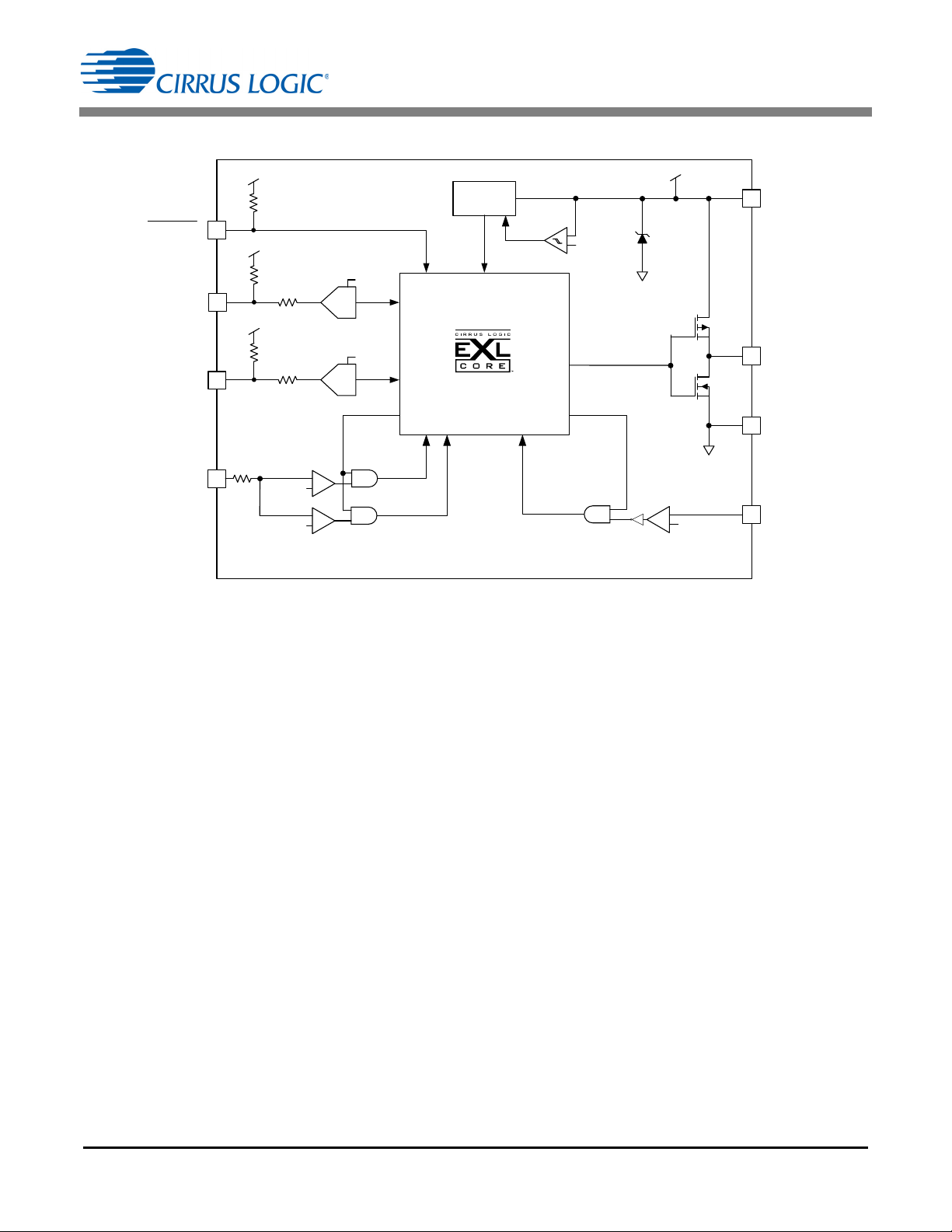
1. INTRODUCTION
V
Z
POR +
-
V
DD ( on)
V
DD ( off)
Volt age
Regulator
8
VDD
5
ZCD
+
-
V
ZCD(th)
7
GD
Zero Crossing
Detect
6
GND
IFB
IAC
V
DD
t
LEB
V
DD
15 k
24 k
3
V
DD
15 k
24 k
1
ADC
ADC
t
ZCB
4
CS
600
+
-
CS
Thresho ld
+
-
CS Clamp
V
CS (c lamp )
V
CS (t h)
STBY
V
DD
600 k
2
I
ref
I
ref
CS1501
Figure 1. CS1501 Block Diagram
The CS1501 digital power factor correction (PFC) control IC is
designed to deliver the lowest system cost by reducing the
total number of system components and optimizing the EMI
noise signature, which reduces the conducted EMI filter
requirements. The CS1501 digital algorithm determines the
behavior of the boost converter during startup, normal
operation, and under fault conditions (overvoltage,
overcurrent, and overtemperature).
Figure 1 illustrates a high-level block diagram of the CS1501.
The PFC processor logic regulates the power transfer by
using an adaptive digital algorithm to optimize the PFC
active-switch (MOSFET) drive signal duty cycle and switching
frequency. The adaptive controller uses independent
analog-to-digital converter (ADC) channels when sensing the
feedback and feedforward analog signals required to
implement the digital PFC control algorithm.
The AC mains rectified voltage (on pin IAC) and PFC output
link voltage (on pin IFB) are transformed by the PFC
processor logic and used to generate the optimum PFC
active-switch drive signal (GD) by calculating the optimal
switching frequency and t
An auxiliary winding is typically added to the PFC boost
inductor to provide zero-current detection (ZCD) information.
time on a cycle-by-cycle basis.
ON
The ZCD acts as a demagnetization sensor used to monitor
the PFC active-switching behavior and efficiency. The
auxiliary voltage is normalized using an external attenuator
and is connected to the ZCD pin, providing the CS1501 a
mechanism to detect the valley/zero crossings. The ZCD
comparator looks for the zero crossing on the auxiliary winding
and switches when the auxiliary voltage is below zero.
Switching in the valley of the oscillation minimizes the
switching losses and reduces EMI noise.
The PFC controller uses a current sensor for overcurrent
protection. The boost inductor peak current is measured
across an external resistor in the switching circuit on a
cycle-by-cycle basis. An overcurrent fault is generated when
the sense voltage applied to the CS pin exceeds a predefined
reference voltage.
The CS1501 includes a supervisor and protection circuit to
manage startup, shutdown, and fault conditions. The
protection circuit is designed to prevent output overvoltage as
a result of load and AC mains transients. The PFC power
converter main rectified voltage (V
(V
) are monitored for overvoltage faults which would lead to
link
shutdown of the PFC controller. The PFC overvoltage
) and output link voltage
rect
protection is designed for auto-recovery; operation resumes
once the fault clears.
2 DS927F4
Page 3
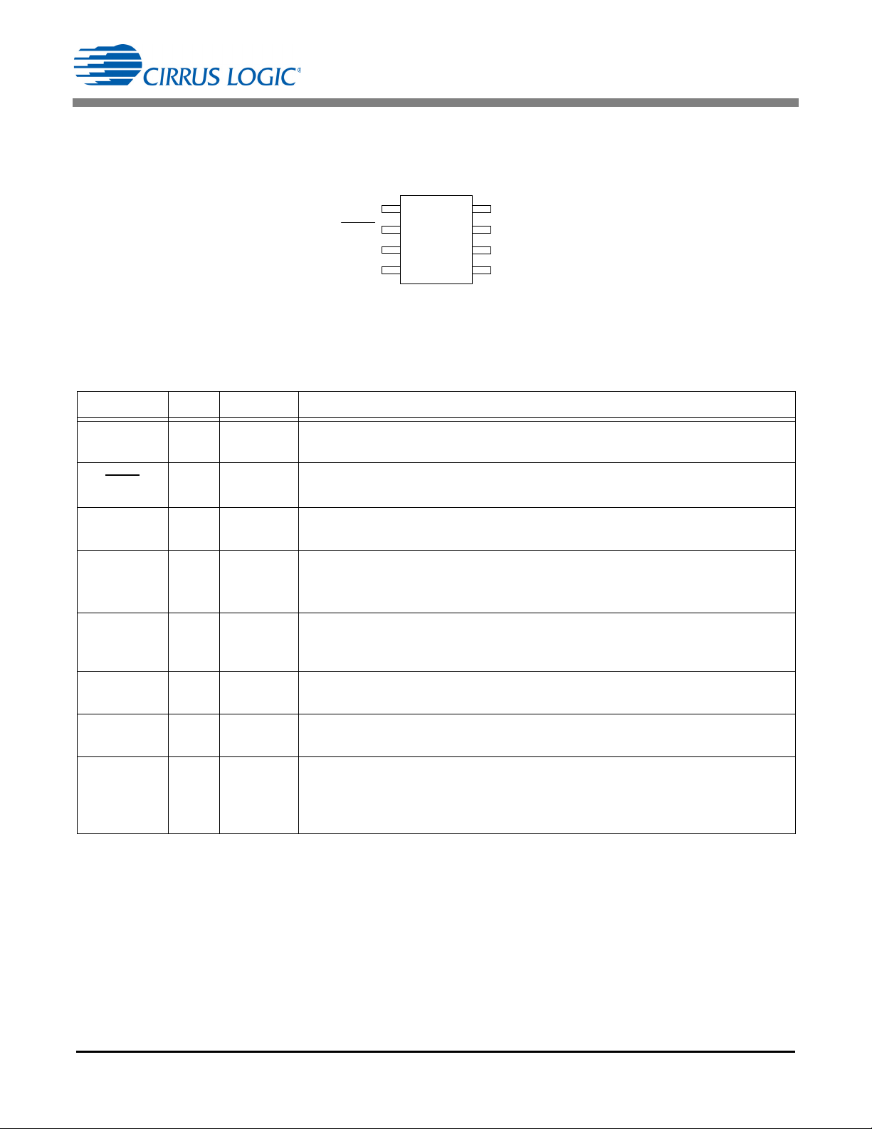
2. PIN DESCRIPTION
CSPFC Current Sense
IFBLink Voltage Sens e
ZCD PFC Zero-current Detect
GND
Ground
GD P FC Ga te D r iv er
VDD IC Supply V oltage
STBYStandby
IA CRectifier Voltage S ense
4
3
2
1
5
6
7
8
8-lead SOIC
Figure 2. CS1501 Pin Assignments
CS1501
Pin Name
IFB
STBY
IAC
CS
ZCD
GND
GD
V
DD
Pin # I/O
1IN
2IN
3IN
4IN
5IN
6PWR
7OUT
8PWR
Description
Link Voltage Sense — A current proportional to the output link voltage of the PFC is
input here. The current is measured with an ADC.
Standby — A voltage below 0.8V puts the IC into a non-operating, low-power state.
The input has an internal 600k pull-up resistor to the V
Rectifier Voltage Sense — A current proportional to the rectified line voltage is input
here. The current is measured with an ADC.
PFC Current Sense — The current flowing in the PFC MOSFET is sensed through a
resistor. The resulting voltage is applied to this pin and digitized for use by the PFC
computational logic to limit the maximum current through the power FET.
PFC Zero-current Detect — Boost Inductor demagnetization sensing input for
zero-current detection (ZCD) information. The pin is externally connected to the PFC
boost inductor auxiliary winding through an external resistor divider.
Ground — Common reference. Current return for both the input signal portion of the IC
and the gate driver.
PFC Gate Driver — The totem pole stage is able to drive the power MOSFET with a
peak current of 0.5A source and 1.0A sink.
IC Supply Voltage — Supply voltage of both the input signal portion of the IC and the
gate driver. A storage capacitor is connected on this pin to serve as a reservoir for operating current for the device, including the gate drive current to the power transistor. This
pin is clamped to a maximum voltage (V
) by an internal zener function.
z
DD
pin.
DS927F4 3
Page 4
3. CHARACTERISTICS AND SPECIFICATIONS
3.1 Electrical Characteristics
Typical characteristics conditions:
TA=25°C, VDD= 13V, GND = 0V
All voltages are measured with respect to GND.
Unless otherwise specified, all currents are positive when
flowing into the IC.
Parameter Condition Symbol Min Typ Max Unit
V
Supply Voltage
DD
Operating Range After Turn-on V
Turn-on Threshold Voltage V
Turn-off Threshold Voltage (UVLO) V
Increasing V
DD
Decreasing V
DD
UVLO Hysteresis V
Zener Voltage I
V
Supply Current
DD
=20mA V
DD
Startup Supply Current VDD=V
Operating Supply Current
4
CL= 1nF, fsw = 70kHz I
Standby Supply Current STBY
Reference
Reference Current I
PFC Gate Drive
Output Source Resistance I
Output Sink Resistance I
Rise Time
Fall Time
4
4
Output Voltage Low State I
Output Voltage High State I
= 100mA, VDD=13V R
GD
= -200mA, VDD=13V R
GD
CL=1nF,VDD=13V t
CL=1nF,VDD=13V t
= -200mA, VDD=13V Vol - 0.9 1.3 V
GD
= 100mA, VDD=13V Voh 11.3 11.8 - V
GD
Zero-current Detection (ZCD)
ZCD Threshold V
ZCD Blanking t
ZCD Sink Current
Upper Voltage Clamp I
1
=1mA V
ZCD
Overvoltage Protection (OVP)
IFB Current at Startup Mode I
IFB Current at Normal Mode I
OVP Threshold I
OVP Hysteresis I
=129AI
ref
=129AI
ref
Overcurrent Protection (OCP)
Current Sense Reference Clamp V
Threshold on Current Sense V
Leading Edge Blanking t
Delay to Output t
Minimum/Maximum characteristics conditions:
TJ= -40° to +125°C, VDD= 10V to 15V, GND = 0 V
DD(on)
< 0.8V I
IFB(startup)
IFB(norm)
DD
DD(on)
DD(off)
Hys
Z
I
ST
DD
SB
ref
OH
OL
r
f
ZCD(th)
ZCB
I
ZCD
CLP
OVP
OVP(Hy)
CS(clamp)
CS(th)
LEB
CS
CS1501
7.9 - 17.0 V
9.8 10.2 10.5 V
7.9 8.1 8.3 V
-2.1-V
17.0 17.9 19.0 V
-6895A
-1.52.1mA
-80125A
- 129 - A
-9-
-6-
-3250ns
-1527ns
-50-mV
- 200 - ns
-2 - - mA
-VDD-V
-116-A
- 129 - A
- 136 - A
-2-A
-1.0-V
-0.5-V
- 300 - ns
-60350ns
4 DS927F4
Page 5
CS1501
GD OUT
GD
GND
CS
VDD
Buffer
S
1
R
1
R
2
R
3
TP
C
L
1nF
+15V
-15V
S
2
V
DD
Parameter Condition Symbol Min Typ Max Unit
Brownout Protection (BP)
Input Brownout Protection Threshold Gate Drive Turns Off I
Input Brownout Recovery Threshold Gate Drive Turns On I
Thermal Protection
2
Thermal Shutdown Threshold T
Thermal Shutdown Hysteresis T
STBY Input
3
BP(lower)
BP(upper)
SD
SD(Hy)
Logic Threshold Low - - 0.8 V
Logic Threshold High V
Notes: 1. External circuitry should be designed to ensure the ZCD sink current pulled from the internal clamp diode when it
is forward biased does not exceed specification.
2. Specifications guaranteed by design and are characterized and correlated using statistical process methods.
3. STBY
4. For test purposes, load capacitance (C
is designed to be driven by an open collector. The input is internally pulled up with a 600 k resistor.
) is 1nF and is connected as shown in the following diagram.
L
-31.6-A
-39.6-A
134 147 159 °C
-9-°C
-0.8 - - V
DD
DS927F4 5
Page 6

CS1501
3.2 Absolute Maximum Ratings
Characteristics conditions:
All voltages are measured with respect to GND.
Pin Symbol Parameter Value Unit
8V
DD
1,2.3,4,5 - Analog Input Maximum Voltage -0.5 to (VDD+0.5) V
1,2,3,4,5 - Analog Input Maximum Current 50 mA
7V
GD
7IGDGate Drive Output Current -1.0 / +0.5 A
-P
-
-T
-T
-T
Stg
All Pins ESD
IC Supply Voltage 19 V
Gate Drive Output Voltage -0.3 to (VDD+0.3) V
Total Power Dissipation @ TA=50°C 600 mW
D
Junction-to-Ambient Thermal Impedance 107 °C /W
JA
Operating Ambient Temperature Range -40 to +125 °C
A
J
Junction Temperature Operating Range
5
-40 to +125 °C
Storage Temperature Range -65 to +150 °C
Electrostatic Discharge Capability Human Body Model
Charged Device Model
2000
500
V
V
Notes: 5. Long-term operation at the maximum junction temperature will result in reduced product life. Derate internal power
dissipation at the rate of 50mW/ °C for variation over temperature.
WARNING:
Operation at or beyond these limits may result in permanent damage to the device.
Normal operation is not guaranteed at these extremes.
6 DS927F4
Page 7

4. TYPICAL ELECTRICAL PERFORMANCE
-3.0%
-2.5%
-2.0%
-1.5%
-1.0%
-0.5%
0.0%
0.5%
-50 0 50 100 150
I
ref
Drift
Temperature (oC)
Figure 3. Supply Current vs. Supply Voltage
Figure 4. Supply Current (ISB, IST, IDD) vs. Temp
Figure 5. UVLO Hysteresis vs. Temp Figure 6. Turn-on & Turn-off Threshold vs. Temp
Figure 7. Reference Current (I
ref
) Drift vs. Temp
0.
0.5
1.
1.5
2.
2.5
3.
3.5
0 2 4 6 8 10 12 14 16 18
I
DD
(mA)
VDD(V)
Rising
Falling
0
0.2
0.4
0.6
0.8
1
1.2
1.4
1.6
1.8
2
-50 0 50 100 150
Supply Current (mA)
Temperature (oC)
f
SW(max)
= 70kHz
Operating
0
1
2
3
-40 0 40 80 120
Temperature (OC)
UVLO Hysteresis
Temperature (OC)
7
7.5
8
8.5
9
9.5
10
10.5
11
-60 -10 40 90 140
VDD (V)
Temperature (OC)
Turn On
Turn Off
CS1501
Start-up
DS927F4 7
Page 8

CS1501
0
2
4
6
8
10
12
14
-60 -40 -20 0 40 100 120 140
Gate Resistor (ROH, ROL) Temp (oC)
Z
out
(Ohm)
Source
Sink
VDD = 13 V
I
source
= 100 mA
I
sink
= 200 mA
20 60 80
Figure 8. Gate Resistance (ROH, ROL) vs. Temp
Figure 10. OVP vs. Temp
96%
98%
100%
102%
104%
106%
-50 0 50 100 150
V
link
(Normalized at 25
O
C)
Temperature (OC)
Normal
OVP
Normal
OVP
17
17.5
18
18.5
19
-50 0 50 100 150
V
Z
(V)
Temperature (oC)
IDD= 20 mA
Figure 9. VDD Zener Voltage vs. Temp
8 DS927F4
Page 9

5. GENERAL DESCRIPTION
0
20
40
60
80
100
120
0 45 90 135 180
Rectified Line Voltage Phase (Deg.)
% of Max
Switching Freq. (% of Max.)
Line Voltage (% of Max.)
% P
O max
F
SW max
(kHz)
Vin < 181 VA C
20
70
50
60
40
405
Burst M ode
20
0
60 80 100
Vin > 147 VA C
46
56
DCM Quasi CRM DCM Quasi CRM DCM
I
LB
t [ms]
I
AC
Inductor Current
t [ms]
V
link
[V]
100%
90%
Startup Mode
Normal
Mode
Startup Mode
Normal
Mode
The CS1501 offers numerous features, options, and
functional capabilities to the designer of switching power
converters. This digital power factor correction (PFC) control
IC is designed to replace legacy analog PFC controllers with
minimal design effort.
5.1 PFC Operation
One key feature of the CS1501 is its operating frequency
profile. Figure 10 illustrates how the frequency varies over a
half cycle of the line voltage in steady-state operation. When
power is first applied to the CS1501, it examines the line
voltage and adapts its operating frequency to the line voltage,
as shown in Figure 10. The operating frequency is varied from
the peak to the trough of the AC input. During startup, the
control algorithm generates maximum power while operating
in critical conduction mode (CRM), providing an approximate
square-wave current envelope within every half-line cycle.
CS1501
mode (quasi-CRM) at low line. For example, at 90 VAC main
input under full load, the PFC controller will function as a
quasi-CRM controller at the peak of the AC line cycle, as
shown in Figure 12.
Figure 12. DCM and Quasi-CRM Operation with CS1501
The zero-current detection (ZCD) of the boost inductor is
achieved using an auxiliary winding. When the stored energy
of the inductor is fully released to the output, the voltage on the
ZCD pin decreases, triggering a new switching cycle. This
quasi-resonant switching allows the active switch to be turned
on with near-zero inductor current, resulting in a nearly
lossless switch event. This minimizes turn-on losses and EMI
noise created by the switching cycle. Power factor correction
control is achieved during light load by using on-time
modulation.
Figure 10. Switching Frequency vs. Phase Angle
Figure 11 illustrates how the operating frequency of the 1501
(as a percentage of maximum frequency) changes with output
power and the peak of the line voltage.
Figure 11. Max. Switching Frequency vs. Output Power
When P
(Refer to section 5.3 Burst Mode on page 10 for more
information.)
The CS1501 is designed to function as a DCM controller.
However, during peak periods, the controller may interchange
control methods and operate in a quasi-critical-conduction
DS927F4 9
falls below 5%, the CS1501 changes to Burst Mode.
O
5.2 Startup vs. Normal Operation Mode
The CS1501 has two discrete operation modes: startup and
normal. Startup mode will be activated when V
90% of nominal value, V
O(startup)
, and remains active until V
reaches 100% of nominal value, as shown in Figure 13.
Startup mode is activated during initial system power-up. Any
drop to less than V
V
link
O(startup)
, such as a load change, can
cause the system to enter startup mode until V
back into regulation.
Figure 13. Startup and Normal Modes
Startup mode is defined as a surge of current delivering
maximum power to the output regardless of the load. During
every active switch cycle, the 'ON' time is calculated to drive a
constant peak current over the entire line cycle. However, the
'OFF' time is calculated based on the DCM/CCM boundary
equation.
is less than
link
is brought
link
link
Page 10

CS1501
V
in
[V]
t [ms]
FET
V
gs
Burst Mode
Active
V
in
P
o
[W]
t [ms]
PFC
Disable
Burst Threshold
Po
V
in min
2
V
link
V
in min
2–
2f
maxLBVlink
---------------------------------------------------------
=
[Eq.1]
Po 90V
2
400V 90V 2–
270kHz L
B
400V
-------------------------------------------------------------
=
[Eq.2]
LB 90V2
400V 90V 2–
270kHzP
o
400V
-------------------------------------------------------------
=
[Eq.3]
V
AC(rms)
90 265
P
o(max)
L > LB
L = L
B
L < LB
IFB
VDD
15 k
8
V
link
CS1501
24 k
ADC
R5
R
IFB
I
FB
R6
1
I
ref
5.3 Burst Mode
Burst mode is used to improve system efficiency when the
Solving Equation 2 for the PFC boost inductor, L
following equation:
, gives the
B
system output power (Po) is <5% of nominal. Burst mode is
implemented by intermittently disabling the PFC over a full
half-line period under light-load conditions, as shown in
Figure 14.
If a value of the boost inductor other than that obtained from
Equation 3 above is used, the total output power capability
and the minimum input voltage threshold will differ according
to Equation 2. Note that if the input voltage drops below
90Vrms and the inductance value is <L
, the link voltage V
B
will drop below 400V and fall out of regulation.
Figure 14. Burst Mode
5.4 Output Power and PFC Boost Inductor
In normal operating mode, the nominal output power is
estimated by the following equation:
where:
P
o
rated output power of the system
efficiency of the boost converter (estimated as 100%
by the PFC algorithm)
V
minimum RMS line voltage is 90V, measured after
in(min)
the rectifier and EMI filter
V
f
max
L
B
nominal PFC output voltage (must be 400V)
link
maximum switching frequency is 70kHz
boost inductor specified by rated power requirement
<1 margin factor to guarantee rated output power (P
against boost inductor tolerances.
Equation 1 is provided for explanation purposes only. Using
substituted required design values for V
link
and f
gives the
max
following equation:
Changing the value for the V
10 DS927F4
voltage is not recommended.
link
Figure 15. Relative Effects of Varying Boost Inductance
5.5 PFC Output Capacitor
The value of the PFC output capacitor needs to be selected
based upon voltage ripple and hold-up requirements. To
ensure system stability with the digital controller, the
recommended value of the capacitor is within the range of
0.5F/watt to 2.0F/watt with a V
voltage of 400V.
link
5.6 Output IFB Sense and Input IAC Sense
A current proportional to the PFC output voltage, V
supplied to the IC on pin IFB and is used as a feedback control
signal. This current is compared against an internal
fixed-value reference current.
The ADC is used to measure the magnitude of the I
through resistor R
compared to an internal reference current (I
)
o
. The magnitude of the I
IFB
IFB
ref
Figure 16. IFB Input Pin Model
) of 129A.
link
current
IFB
current is then
link
, is
Page 11

CS1501
R
IFB
V
linkVDD
–
I
ref
-----------------------------
400V V
DD
–
129 A
-------------------------------==
[Eq.4]
R1
R
IAC
I
AC
IA C
VDD
15 k
8
V
rect
CS1501
24 k
ADC
R2
3
I
ref
R
IAC
R
IFB
=
[Eq.5]
R3
I
Aux
V
link
ZCD
L
B
R4
CS1501
ZCD_below_zero
D2
FE T Dra in
N:1
+
V
Aux
-
Demag
Comparator
+
-
V
th( ZC D)
5
I
ZCD
C
p
ZCD
Zero Crossing
Detection
GD ‘ON’
ZCD_below _zero
fc12 R3 R4
C
p
=
[Eq.6]
Resistor R
sets the feedback current and is calculated as
IFB
follows:
By using digital loop compensation, the voltage feedback
signal does not require an external compensation network.
A current proportional to the AC input voltage is supplied to the
IC on pin IAC and is used by the PFC control algorithm.
Figure 17. IAC Input Pin Model
Resistor R
For optimal performance, resistors R
1% tolerance or better resistors for best V
sets the IAC current and is derived as follows:
IAC
IAC
and R
link
should use
IFB
voltage accuracy.
5.7 Valley Switching
The zero-current detection (ZCD) pin is monitored for
demagnetization in the auxiliary winding of the boost inductor
). The ZCD circuit is designed to detect the V
(L
B
valley/zero crossings by sensing the voltage transformed onto
the auxiliary winding of LB.
Aux
MOSFET switching cycle when its drain-source voltage is at
the lowest possible voltage potential, thus reducing switching
losses. The CS1501 uses an auxiliary winding on the PFC
boost inductor to implement zero-voltage switching.
Figure 19. Zero-voltage Switch
During each switching cycle, when the boost diode current
reaches zero, the boost MOSFET drain-source voltage begins
oscillating at the resonant frequency of the boost inductor and
MOSFET parasitic output capacitance. The ZCD_below_zero
signal transitions from high to low just prior to a local minimum
of the MOSFET drain-source voltage oscillation. The
zero-crossing detect circuit ensures that a ZCD_below_zero
pulse will only be generated when the comparator output is
continuously high for a nominal time period (t
) of 200ns.
ZCB
Therefore, any negative edges on the comparator's output
due to spurious glitches will not cause a pulse to be
generated. Due to the CS1501’s variable-frequency control,
the MOSFET switching cycle will not always be initiated at the
first resonant valley.
The external circuitry should be designed so that the current
) at the ZCD pin is approximately 1.0 mA. The table
(I
ZCD
below depicts approximate values for R3 and R4 for a range
of boost-to-auxiliary inductor turns ratio, N.
N~R3~R4
946k 1.75k
10 42 k 1.75k
11 37.5 k 1.75k
12 35.5 k 1.75k
13 32 k 1.75k
14 29.5 k 1.75k
15 27.5 k 1.75k
Table 1. Aux Inductor Turns Ratio vs. R3 and R4
The objective of zero-voltage switching is to initiate each
DS927F4 11
Figure 18. ZCD Input Pin Model
Resistors R3 and R4 were calculated using V
C
=10pF.
p
= 400V and
link
Equation 6 is used to calculate the cut-off frequency defined
by the RC circuit at the ZCD pin.
where:
f
c
The cut-off frequency, fc, needs to be 10x the ringing
frequency
C
Capacitance at the ZCD pin
p
Page 12
CS1501
56 ms
56 ms
Start
Timer
Enter Standby Exit Standby
Upper
Lower
Brownout
Thresholds
Start Timer
T
Brownout
T
Brownout
8ms
8ms
5V
------------
128 V V
BP th
–56 ms++=
[Eq.7]
8=
8
5
--- 128 94.8–56++117ms=
V
OVP
R
IFBIOVP
VDD+=
[Eq.8]
5.8 Brownout Protection
The CS1501 brownout detection circuit monitors the peak of
the V
it drops below a predetermined threshold. Hysteresis and
minimum detection time are provided to avoid brownout
detection during short input transients. When brownout is
detected, the CS1501 enters standby mode. On recovery from
brownout, it re-enters normal operating mode.
Current I
V
page 11). The digitized current applied to the IAC pin is
monitored by the brownout protection algorithm. When V
drops below the brownout-detection threshold, the CS1501
triggers a timer. The IC asserts the brownout protection and
stops the gate-drive switching only if the timer exceeds 56ms.
This is the equivalent of 7 rectified line cycles at 60 Hz.
During the brownout state, the device continues monitoring
the input line voltage. The device exits the brownout state
when I
56ms. Typical values for the lower (I
(I
respectively.
The overpower protection may activate prior to brownout
protection, depending on the load.
input voltage and disables the PWM switching when
rect
is proportional to the AC input voltage V
AC
rect=RIACxIAC
AC
BP(upper)
and R
=R1+R2 (see Figure 17 on
IAC
exceeds the brownout upper threshold for at least
) brownout thresholds are 31.6A and 39.6 A,
BP(lower)
,where
rect
rect
) and upper
5.9 Overvoltage Protection
The overvoltage protection (OVP) will trigger immediately and
stop the gate drive when the current into the IFB pin (I
exceeds 105% of the reference current (I
) value. The IC
ref
OVP
resumes gate drive switching when the measured current at IFB
drops below I
OVP–IOVP(Hy)
. Equation 8 is used to calculate the
OVP threshold.
5.10 Overcurrent Protection
To limit boost inductor current through the FET and to prevent
boost inductor saturation conditions, the CS1501 incorporates
a cycle-by-cycle peak inductor current limit circuit using an
external shunt resistor to ‘sense’ the FET source current
accurately. The overcurrent protection (OCP) circuit is
designed to monitor the current when the active switch is
turned on. The OCP circuit is enabled after the leading-edge
blanking time (t
reference voltage, V
overcurrent condition exists. The OCP circuit triggers
immediately, allowing the OCP algorithm to turn off the gate
driver.
The overcurrent protection circuit is also designed to monitor
for a catastrophic overcurrent occurrence by sensing sudden
and abnormal operating currents. A second OCP threshold,
V
cs(clamp)
, determines whether a severe overcurrent condition
exists. This immediately turns off the gate drive, and the
system enters a restart mode. The CS1501 inhibits all
switching operations for approximately 1.6ms then attempts to
restart normal operation.
). The shunt voltage is compared to a
LEB
, to determine whether an
cs(th)
)
5.11 Overpower Protection
Figure 20. Brownout Sequence
The maximum response time of the brownout protection
feature occurs at light-load conditions. It is calculated by
Equation 7.
where:
V
12 DS927F4
Brownout threshold voltage, V
BP(th)
BP(th) =IBP(lower)xRIAC
The CS1501 incorporates an internal overpower protection
(OPP) algorithm that provides protection from overload
conditions. This algorithm uses the condition that output
power is a function of the boost inductor (see section 5.4
Output Power and PFC Boost Inductor on page 10).
Under moderate overload, V
may droop up to 10% while
link
maintaining rated power and PFC. Further increasing the load
current causes V
to drop below the startup threshold
link
(~360V). Below this threshold, the circuit switches the
operating mode to startup with more power available to raise
V
link
. As V
reaches its nominal value, startup mode is
link
canceled and power is now limited to the rated value. If the
overload is still present, this cycle will repeat.
If a sustained overload, or a repeated cycle of overload events
is detected for greater than 112 ms, the CS1501 shuts down
for 2.5 seconds, then attempts to restart.
Page 13

CS1501
<1 nF
600 k
See Tex t
VDD
STBY
GND
CS1 501
8
6
2
5.12 Open/ Short Loop Protection
If the PFC output sense resistor, R
GND), the measured output voltage decreases at a slew rate of
about 2 V/s, which is determined by the ADC sampling rate.
The IC stops the gate drive when the measured output voltage is
lower than the measured line voltage. The IC resumes gate drive
switching when the current into the IFB pin becomes larger than
or equal to the current into the IAC pin and V
the peak of the line voltage (V
rect(pk)
time of open/short loop protection for R
If the PFC input sense resistor R
the current reference signal supplied to the IC on pin IAC falls
to zero.
, fails (open or short to
IFB
is greater than
link
). The maximum response
is about 150s.
IFB
fails (open or short to GND),
IAC
5.13 Internal Overtemperature Protection
An internal thermal sensor triggers a shutdown when the
temperature exceeds 135°C (nominal) on the silicon. The
sensor sends a signal to the core that supplies current to all
internal digital logic, cutting off power from them. Once the
temperature of the IC has dropped by 9 ° C (nominal), the
sensor resets, allowing power to the logic.
5.14 Standby (STBY) Function
The standby (STBY) pin provides a means by which an
external signal can cause the CS1501 to enter a
non-operating, low-power state. The STBY
be driven by an open-collector/open-drain device. Internal to
the pin, there is a pull-up resistor connected to the VDD pin, as
shown in Figure 21. Since the pull-up resistor has a high
impedance, a filter capacitor (up to 1000pF) may be required
on this pin.
Figure 21. STBY Pin Connection
When the STBY
be tied to V
pin is not used, it is recommended that the pin
(pulled high).
DD
input is intended to
DS927F4 13
Page 14
5.15 Summary of Equations
Po
V
in min
2
V
link
V
in min
2–
2f
maxLBVlink
---------------------------------------------------------
=
Po 90Vrms2
400V 90V rms 2–
270kHz L
B
400V
-------------------------------------------------------------
=
LB 90Vrms2
400V 90V rms 2–
270kHzP
o
400V
-------------------------------------------------------------
=
R
IFB
V
linkVDD
–
I
ref
-----------------------------
400V V
DD
–
129 A
-------------------------------
==
R
IAC
R
IFB
=
fc12 R3 R4
C
p
=
T
Brownout
8ms
8ms
5V
------------
128 V V
BP th
–56 ms++=
V
OVP
R
IFBIOVP
VDD+=
I
LB pk
4P
O
V
in min
2
--------------------------------------------
=
I
LB rms
P
O
V
in min
------------------------------
=
V
link rip
P
O
2 f
line min
V
link
C
out
------------------------------------------------------------------------
=
Eq. # Equation Variables/Recommended Values
Output Power (page 10
1
Output Power with recommended values (page 10
)
P
o
Rated output power of the system.
Efficiency of the boost converter (estimated as
100% by the PFC algorithm).
)
CS1501
2
V
in(min)
Minimum RMS line voltage is 90Vrms,
measured after the rectifier and EMI filter.
Boost Inductor (page 10
3
Output IFB Sense Resistor (page 11
)
)
V
f
max
L
link
B
Nominal PFC output voltage must be 400V.
Maximum switching frequency is 70kHz.
Boost inductor specified by rated power
requirement.
4
Margin factor to guarantee rated output power
(P
) against boost inductor tolerances.
Input IAC Sense Resistor (page 11
5
Auxiliary Winding Cut-off Frequency (page 11
)
R
IAC
)
R
IFB
o
Value of the IAC pin sense resistor(s).
Value of the IFB pin sense resistor(s).
6
I
ref
Maximum Response Time for Brownout: (page 12
)
f
c
7
Value of the fixed, internal reference current.
The cut-off frequency, fc, needs to be 10x the
ringing frequency or fc = 10MHz.
C
Capacitance at the ZCD pin. Cp<10pF.
p
Overvoltage Protection (page 12)
8
Boost Inductor Peak Current
V
BP(th)
C
out
Brownout threshold voltage. V
BP(th)
Value of the output capacitor in mF.
=94.8V.
9
Boost Inductor RMS Current
f
line(min)
V
DD
Minimum line frequency.
IC Supply Voltage.
10
V
OVP
V
Voltage Ripple
link
I
11
14 DS927F4
OVP
OVP threshold.
Current into the IFB pin.
Page 15

6. PACKAGE DRAWING
SOIC-8 NARROW (150 MIL BODY) PACKAGE DRAWING
CS1501
MILLIMETERS INCHES
Dimension MIN NOM MAX MIN NOM MAX
A - - - - 1.75 - - - - 0.069
A1 0.10 - - 0.25 0.004 - - 0.010
b 0.31 - - 0.51 0.012 - - 0.020
c 0.10 - - 0.25 0.004 - - 0.010
D 4.90 BSC 0.193 BSC
E 6.00 BSC 0.236 BSC
E1 3.90 BSC 0.154 BSC
e 1.27 BSC 0.050 BSC
L 0.40 - - 1.27 0.016 - - 0.050
Θ
aaa 0.10 0.004
bbb 0.25 0.010
ddd 0.25 0.010
Notes:
1. Controlling dimensions are in millimeters
2. Dimensions and Tolerances per ASME Y14.5 M
3. This drawing conforms to JEDEC outline MS-012, variation AA for standard SOIC-8 narrow body
4. Recommended reflow profile is per JEDEC/IPC J-STD-020
0° - - 8° 0° - - 8°
DS927F4 15
Page 16

CS1501
Contacting Cirrus Logic Support
For all product questions and inquiries contact a Cirrus Logic Sales Representative.
To find one nearest you go to http://www.cirrus.com
IMPORTANT NOTICE
Cirrus Logic, Inc. and its subsidiaries ("Cirrus") believe that the information contained in this document is accurate and reliable. However, the information is subject
to change without notice and is provided "AS IS" without warranty of any kind (express or implied). Customers are advised to obtain the latest version of relevant
information to verify, before placing orders, that information being relied on is current and complete. All products are sold subject to the terms and conditions of sale
supplied at the time of order acknowledgment, including those pertaining to warranty, indemnification, and limitation of liability. No responsibility is assumed by Cirrus
for the use of this information, including use of this information as the basis for manufacture or sale of any items, or for infringement of patents or other rights of third
parties. This document is the property of Cirrus and by furnishing this information, Cirrus grants no license, express or implied under any patents, mask work rights,
copyrights, trademarks, trade secrets or other intellectual property rights. Cirrus owns the copyrights associated with the information contained herein and gives consent for copies to be made of the information only for use within your organization with respect to Cirrus integrated circuits or other products of Cirrus. This consent
does not extend to other copying such as copying for general distribution, advertising or promotional purposes, or for creating any work for resale.
CERTAIN APPLICATIONS USING SEMICONDUCTOR PRODUCTS MAY INVOLVE POTENTIAL RISKS OF DEATH, PERSONAL INJURY, OR SEVERE PROPERTY OR ENVIRONMENTAL DAMAGE ("CRITICAL APPLICATIONS"). CIRRUS PRODUCTS ARE NOT DESIGNED, AUTHORIZED OR WARRANTED FOR USE
IN PRODUCTS SURGICALLY IMPLANTED INTO THE BODY, AUTOMOTIVE SAFETY OR SECURITY DEVICES, LIFE SUPPORT PRODUCTS OR OTHER CRITICAL APPLICATIONS. INCLUSION OF CIRRUS PRODUCTS IN SUCH APPLICATIONS IS UNDERSTOOD TO BE FULLY AT THE CUSTOMER'S RISK AND
CIRRUS DISCLAIMS AND MAKES NO WARRANTY, EXPRESS, STATUTORY OR IMPLIED, INCLUDING THE IMPLIED WARRANTIES OF MERCHANTABILITY
AND FITNESS FOR PARTICULAR PURPOSE, WITH REGARD TO ANY CIRRUS PRODUCT THAT IS USED IN SUCH A MANNER. IF THE CUSTOMER OR
CUSTOMER'S CUSTOMER USES OR PERMITS THE USE OF CIRRUS PRODUCTS IN CRITICAL APPLICATIONS, CUSTOMER AGREES, BY SUCH USE, TO
FULLY INDEMNIFY CIRRUS, ITS OFFICERS, DIRECTORS, EMPLOYEES, DISTRIBUTORS AND OTHER AGENTS FROM ANY AND ALL LIABILITY, INCLUDING ATTORNEYS' FEES AND COSTS, THAT MAY RESULT FROM OR ARISE IN CONNECTION WITH THESE USES.
Cirrus Logic, Cirrus, the Cirrus Logic logo designs, EXL Core, and the EXL Core logo design are trademarks of Cirrus Logic, Inc. All other brand and product names
in this document may be trademarks or service marks of their respective owners.
7. ORDERING INFORMATION
Part # Temperature Range Package Description
CS1501-FSZ -40°C to +125°C 8-lead SOIC, Lead (Pb) Free
8. ENVIRONMENTAL, MANUFACTURING, & HANDLING INFORMATION
Model Number Peak Reflow Temp MSL Rating
CS1501-FSZ 260°C 2 365 Days
a. MSL (Moisture Sensitivity Level) as specified by IPC/JEDEC J-STD-020.
b. Stored at 30°C, 60% relative humidity.
9. REVISION HISTORY
Revision Date Changes
PP5 MAY 2011 Updated Typical Electrical Performance section.
PP6 JUN 2011 Updated Characteristics and Specifications section.
F1 SEP 2011 Finalized. Updated Characteristics and Specifications section.
F2 JAN 2012 Edited for content and clarity. Corrected typographical errors.
F3 FEB 2012 Revised MSL rating.
F4 FEB 2012 Corrected a typographical error.
a
Max Floor Life
b
16 DS927F4
 Loading...