

Page 1
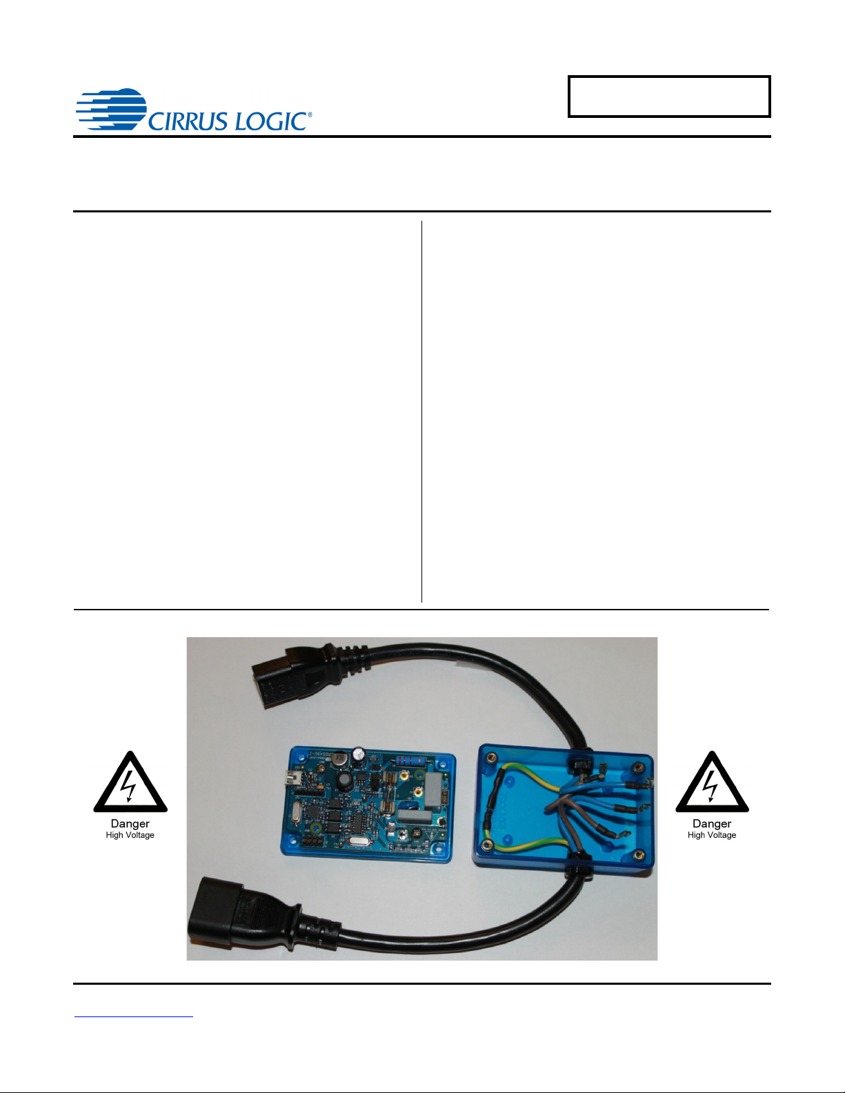
CRD5490-Z Power Monitor
CRD5490-Z
Features
• Easy-to-use Power Monitoring Reference Design
– Plug one side into a wall outlet and an electric load
into the other side.
– Read real time measurements on the PC GUI via
USB in seconds.
• Real Time Measurements:
– Line Voltage
– Load Current
– Active Power
– Reactive Power
– Apparent Power
– Power Factor
– Fundamental Line Frequency
– Temperature
• Operational Voltage 90VAC to 260 VAC
• Maximum RMS Load Current 15A
• Factory Calibrated and Recalibration Capable
• Compact AC/DC Buck Converter
• Onboard PIC18 Microcontroller
• Windows
®
GUI Software
Overview
The CRD5490-Z is designed to evaluate the functionality
and performance of the CS5490 power/energy
measurement device. The CRD5490-Z integrates an
efficient and compact AC/ DC drop capacitor/buck
power supply, voltage and current sensors, and low-cost
USB MCU. This compact, complete power monitor
system integrates easily in any design evaluation.
The CRD5490-Z was designed with a graphical user
interface (GUI) for power measurements and calibration
execution. A full-featured GUI is provided to access real
time line voltage, load current, active power, reactive
power, apparent power, power factor, and temperature.
The software provides full access and control of the
CS5490 calibration and configuration without having to
learn specialized commands.
ORDERING INFORMATION
CRD5490-Z Reference Design
Cirrus Logic, Inc.
http://www.cirrus.com
Copyright Cirrus Logic, Inc. 2012
(All Rights Reserved)
APR‘12
DS988RD1
Page 2
CRD5490-Z
Contacting Cirrus Logic Support
For all product questions and inquiries contact a Cirrus Logic Sales Representative. To find the one nearest to you
go to www.cirrus.com
IMPORTANT NOTICE
Cirrus Logic, Inc. and its subsidiaries ("Cirrus") believe that the information contained in this document is accurate and reliable. However, the information is subject
to change without notice and is provided "AS IS" without warranty of any kind (express or implied). Customers are advised to obtain the latest version of relevant
information to verify, before placing orders, that information being relied on is current and complete. All products are sold subject to the terms and conditions of sale
supplied at the time of order acknowledgment, including those pertaining to warranty, indemnification, and limitation of liability. No responsibility is assumed by Cirrus
for the use of this information, including use of this information as the basis for manufacture or sale of any items, or for infringement of patents or other rights of third
parties. This document is the property of Cirrus and by furnishing this information, Cirrus grants no license, express or implied under any patents, mask work rights,
copyrights, trademarks, trade secrets or other intellectual property rights. Cirrus owns the copyrights associated with the information contained herein and gives
consent for copies to be made of the information only for use within your organization with respect to Cirrus integrated circuits or other products of Cirrus. This consent does not extend to other copying such as copying for general distribution, advertising or promotional purposes, or for creating any work for resale.
CERTAIN APPLICATIONS USING SEMICONDUCTOR PRODUCTS MAY INVOLVE POTENTIAL RISKS OF DEATH, PERSONAL INJURY, OR SEVERE PROPERTY OR ENVIRONMENTAL DAMAGE ("CRITICAL APPLICATIONS"). CIRRUS PRODUCTS ARE NOT DESIGNED, AUTHORIZED OR WARRANTED FOR
USE IN PRODUCTS SURGICALLY IMPLANTED INTO THE BODY, AUTOMOTIVE SAFETY OR SECURITY DEVICES, LIFE SUPPORT PRODUCTS OR OTHER
CRITICAL APPLICATIONS. INCLUSION OF CIRRUS PRODUCTS IN SUCH APPLICATIONS IS UNDERSTOOD TO BE FULLY AT THE CUSTOMER'S RISK
AND CIRRUS DISCLAIMS AND MAKES NO WARRANTY, EXPRESS, STATUTORY OR IMPLIED, INCLUDING THE IMPLIED WARRANTIES OF MERCHANTABILITY AND FITNESS FOR PARTICULAR PURPOSE, WITH REGARD TO ANY CIRRUS PRODUCT THAT IS USED IN SUCH A MANNER. IF THE CUSTOMER
OR CUSTOMER'S CUSTOMER USES OR PERMITS THE USE OF CIRRUS PRODUCTS IN CRITICAL APPLICATIONS, CUSTOMER AGREES, BY SUCH USE,
TO FULLY INDEMNIFY CIRRUS, ITS OFFICERS, DIRECTORS, EMPLOYEES, DISTRIBUTORS AND OTHER AGENTS FROM ANY AND ALL LIABILITY, INCLUDING ATTORNEYS' FEES AND COSTS, THAT MAY RESULT FROM OR ARISE IN CONNECTION WITH THESE USES.
Microsoft Visual Studio, Windows 7, and Windows XP are either trademarks or registered trademarks of Microsoft Corporation.
IMPORTANT SAFETY INSTRUCTIONS
Read and follow all safety instructions prior to using this demonstration board.
This Engineering Evaluation Unit or Demonstration Board must only be used for assessing IC performance in a
laboratory setting. This product is not intended for any other use or incorporation into products for sale.
This product must only be used by qualified technicians or professionals who are trained in the safety procedures
associated with the use of demonstration boards.
Risk of Electric Shock
• The direct connection to the AC power line and the open and unprotected boards present a serious risk of electric
shock and can cause serious injury or death. Extreme caution needs to be exercised while handling this board.
• Avoid contact with the exposed conductor or terminals of components on the board. High voltage is present on
exposed conductor and it may be present on terminals of any components directly or indirectly connected to the AC
line.
• Dangerous voltages and/or currents may be internally generated and accessible at various points across the board.
• Charged capacitors store high voltage, even after the circuit has been disconnected from the AC line.
• Make sure that the power source is off before wiring any connection. Make sure that all connectors are well
connected before the power source is on.
• Follow all laboratory safety procedures established by your employer and relevant safety regulations and guidelines,
such as the ones listed under, OSHA General Industry Regulations - Subpart S and NFPA 70E.
Suitable eye protection must be worn when working with or around demonstration boards. Always
comply with your employer’s policies regarding the use of personal protective equipment.
All components and metallic parts may be extremely hot to touch when electrically active.
2 DS988RD1
Page 3
CRD5490-Z
1. CHARACTERISTICS AND SPECIFICATIONS
1.1 Recommended Operating Conditions
Parameter Symbol Min Typ Max Unit
Reference
Line Voltage V
Load Current
Peak Current I
Fundamental Frequency Freq 5 - 2000 Hz
Ambient Operating Temperature T
AC
I
RMS
PEAK
A
1.2 Electrical Characteristics
Parameter Symbol Min Typ Max Unit
Reference
Power Consumption (V
Accuracy (PF=1, Sample Count 8000 - 2 second, Temp Compensation Enabled)
RMS Voltage (90-260V
RMS Current (15mA-15A)
Active Power (1.5W-3900W)
= 240V, 50Hz) P
AC
)
AC
V
I
P
AC
RMS
RMS
AVG
90 - 260 V
--15A
--22A
-40 85
-0.6-W
-
-
-
0.1
0.1
0.1
-%
-%
-%
C
DS988RD1 3
Page 4
CRD5490-Z
WARNING
High Voltage Hazard
When the CRD5490-Z is connected to AC lines, high voltage is present inside the box.
Do not remove the protective cover from the CRD5490-Z when power is connected.
The evaluation board connects directly to the AC power line and presents a serious risk of
electric shock and can cause serious injury or death. Extreme caution needs to be
exercised while handling this box. Make sure that the power source is off before wiring any
connection. Make sure that all connectors are well connected before the power source is
turned on. Make sure all AC power line wiring is secured to the box and away from contact
before the power source is on.
Refer to additional warnings at the beginning of this document.
AC
Load
Current
Sensor
Voltage
Divide Sensor
+3.3V
Voltage
Input
Current Input
MCU
USB
Cap. Drop
+ Buc k Supply
Isolation
CS5490
CRD5490-Z
RX
RESET
TX
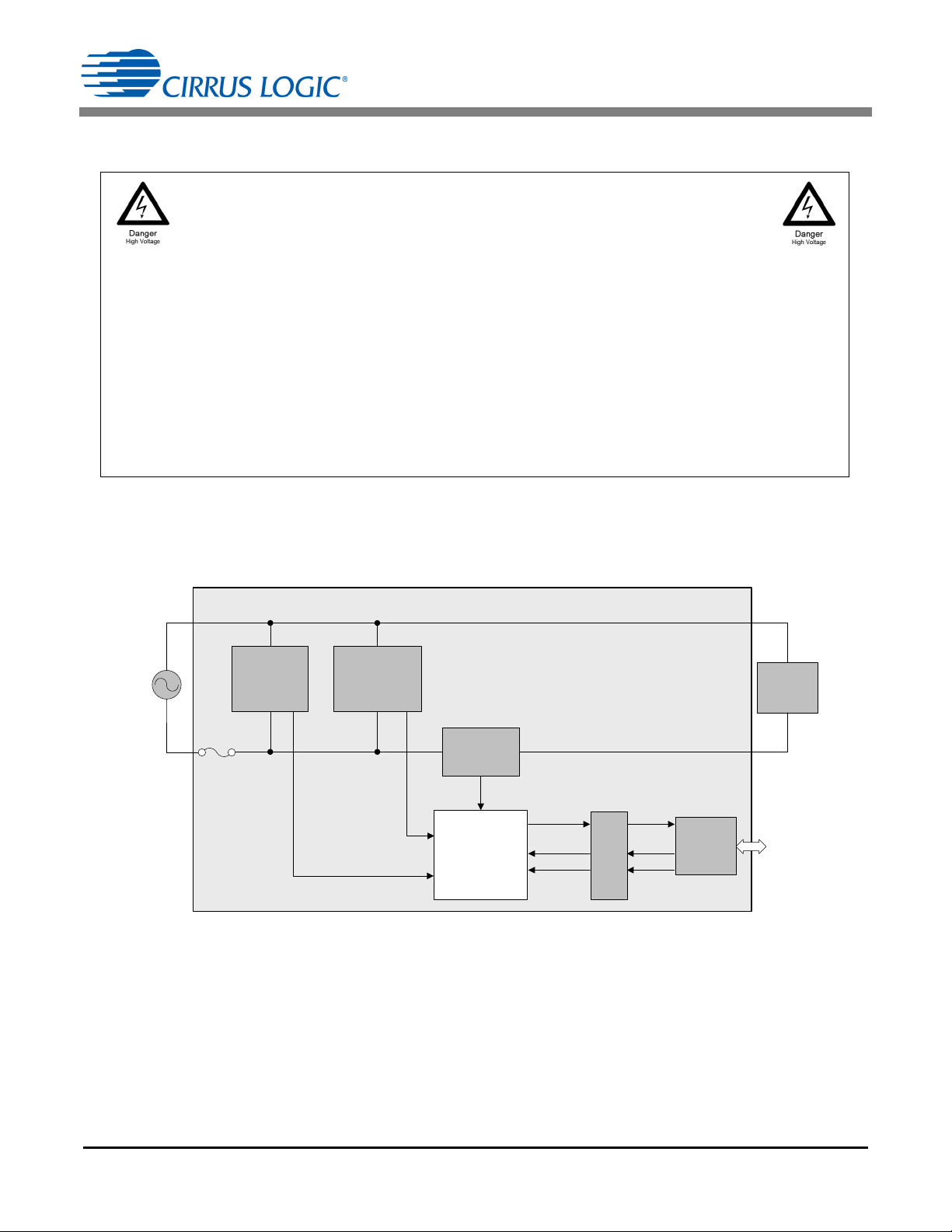
Figure 1. System Block Diagram
2. HARDWARE OVERVIEW
The CRD5490-Z includes sensors (line voltage and current shunt), a power supply, a CS5490 power
monitor calculation engine, isolation, and an MCU. Figure 1 shows connections of each block.
Make sure that the power source is off before wiring any connection. The AC source is connected to plug IEC 60320
C14, and the AC load is connected to connector IEC 60320 C13. Make sure that all connectors are well connected
before the power source is turned on. Make sure all AC power line wiring is secured to the box and away from contact
before the power source is on.
4 DS988RD1
Page 5
CRD5490-Z
R1
R2
VOUT
VIN
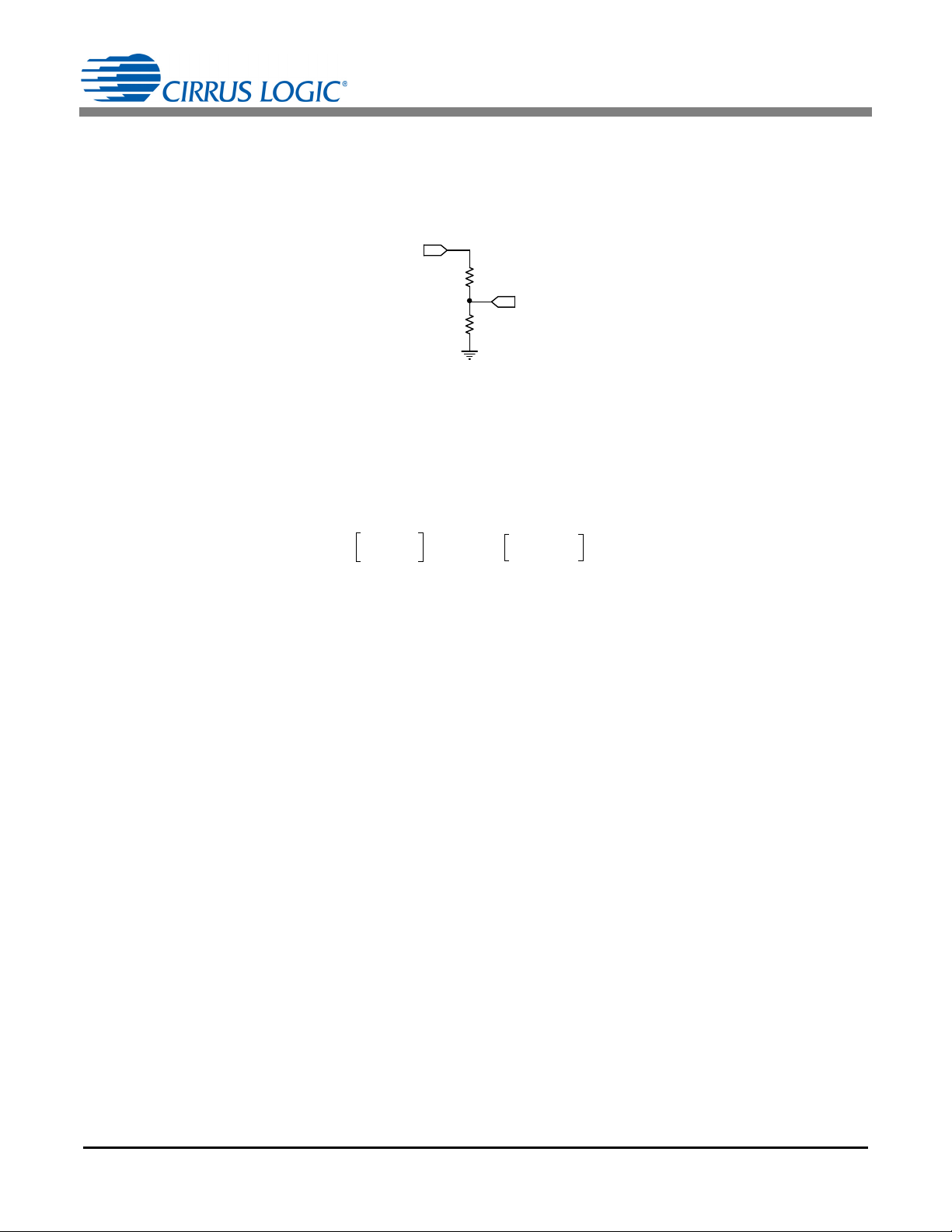
Figure 2. Voltage Sensor Attenuator
V
OUTVIN
R2
R1 R2+
--------------------- -
176m V
RMS
=
Eq. 1
R1 R2
V
IN
V
OUT
--------------
1– 1000
260V
176m V
-------------------
1– 1.47M ===
Eq. 2
R
SHUNT
V
OUT
I
SHUNT
------------------ -
35.36mV
15A
------------------------
2.35m == =
Eq. 3
2.1 Line Voltage Sensor
The high-voltage AC line is attenuated using a voltage divider sensor comprised of five 1206 resistors before being
supplied to the CS5490 voltage channel input. Figure 2 shows the resistor diagram for line voltage sensing. R1 is
actually four large-value resistors, which increases the voltage rating. R2 is one 1K sense resistor. Refer to the
vendor’s specifications for voltage compliance.
The divider ratio is determined by the maximum input range of the CS5490 voltage channel (176mV
RMS
) and the
maximum line voltage. The division ratio is determined by Equation 1.
For a line voltage, V
= 260V
IN
, and R2 = 1K, R1 can be solved. See Equation 2:
RMS
To give a 115% margin and to select common resistor values, R1 = 115% 1.47M is selected and composed of
four resistors: 4 422k.
The voltage sense resistor (R2) must be referenced to the same potential as the current sensor and CS5490 power
supply (located either on the Line or Neutral). By design, the CRD5490-Z is referenced to the Line side after the
fuse. To switch the sensor reference, Line and Neutral of both the load and the source could be switched, and the
fuse should be placed on the line externally.
2.2 Shunt Current Resistor
The CRD5490-Z implements current sensing using a low-resistance shunt. When a shunt is used, the current
channel’s signal amplitude will be set by the shunt resistor using Ohm's Law, V = IR. To keep power dissipation low,
it is necessary to use a low-resistance shunt. The current channel of the CS5490 provides a high gain setting (50x)
to enable the use of a low-valued shunt. The maximum input amplitude for the current channel is 35mV
50x gain range.
Applying Ohm's law, V
OUT
= I
SHUNT
R
, use Equation 3 to solve for R
SHUNT
SHUNT
:
RMS
in the
To give an 85% margin, the shunt should be reduced by R
= 85%2.35m = 2 m. The power rating of the
SHUNT
shunt should be at least twice the power dissipation on the shunt with the maximum continuous load current. With
a maximum 15A load current, the CRD5490-Z uses a 2W shunt resistor.
DS988RD1 5
Page 6
CRD5490-Z
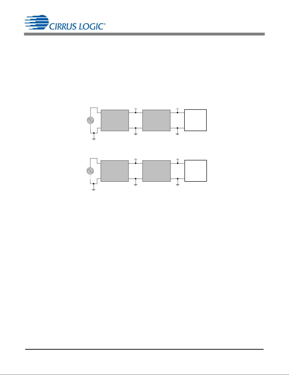
AC
Drop Capacitor
and Rectifier
Buck
Converter
+35 V +3 .3V
CS5490
Figure 3. Power Supply Option 1
AC
Drop Capacitor
and Rectifier
+3.3V
Regulator
+6V +3 .3V
CS5490
Figure 4. Power Supply Option 2
2.3 Power Supply
The CRD5490-Z contains two separate power supply domains: isolated +5V USB supply and +3.3V non-isolated
CS5490 power supply derived from the power line. The +3.3V non-isolated power supply circuit is designed to
reduce the overall supply volume by creating a two-stage drop capacitor and buck supply.
By selecting an efficient buck design instead of a simple voltage regulator, the rectified supply voltage is raised, the
transferred power is increased, and the drop capacitor value is reduced. Reducing the value substantially reduces
the capacitor's size. If size is not a factor, the more expensive buck design could be replaced with a simple voltage
regulator. Figure 3 and Figure 4 show the two options evaluated for the CRD5490-Z design. Contact Cirrus Logic
sales for assistance with a cost-reduced, regulator-only design.
2.4 MCU Purpose
The CRD5490-Z is designed to minimize the requirements of the MCU. Virtually any low-cost MCU with non-volatile
memory (NVM) can be used with the CS5490 device and software. The microchip MCU has the following purposes
in the CRD5490-Z:
– Store and reload calibration coefficients
– Perform USB to UART transactions that mimic a serial COM port
USB transactions are sent from the PC to the MCU. The MCU reads the first byte (character) and determines
whether it should transmit the remaining bytes to the CS5490 as a Write/Read/DSP command or store or recall as
calibration coefficients into NVM. All responses from the CS5490 are directly translated back to the PC via the MCU.
MCU UART communication transactions can be viewed at the bottom of the GUI. Characters sent or received are
displayed in hexadecimal format. Refer to Figure 26.
6 DS988RD1
Page 7
CRD5490-Z
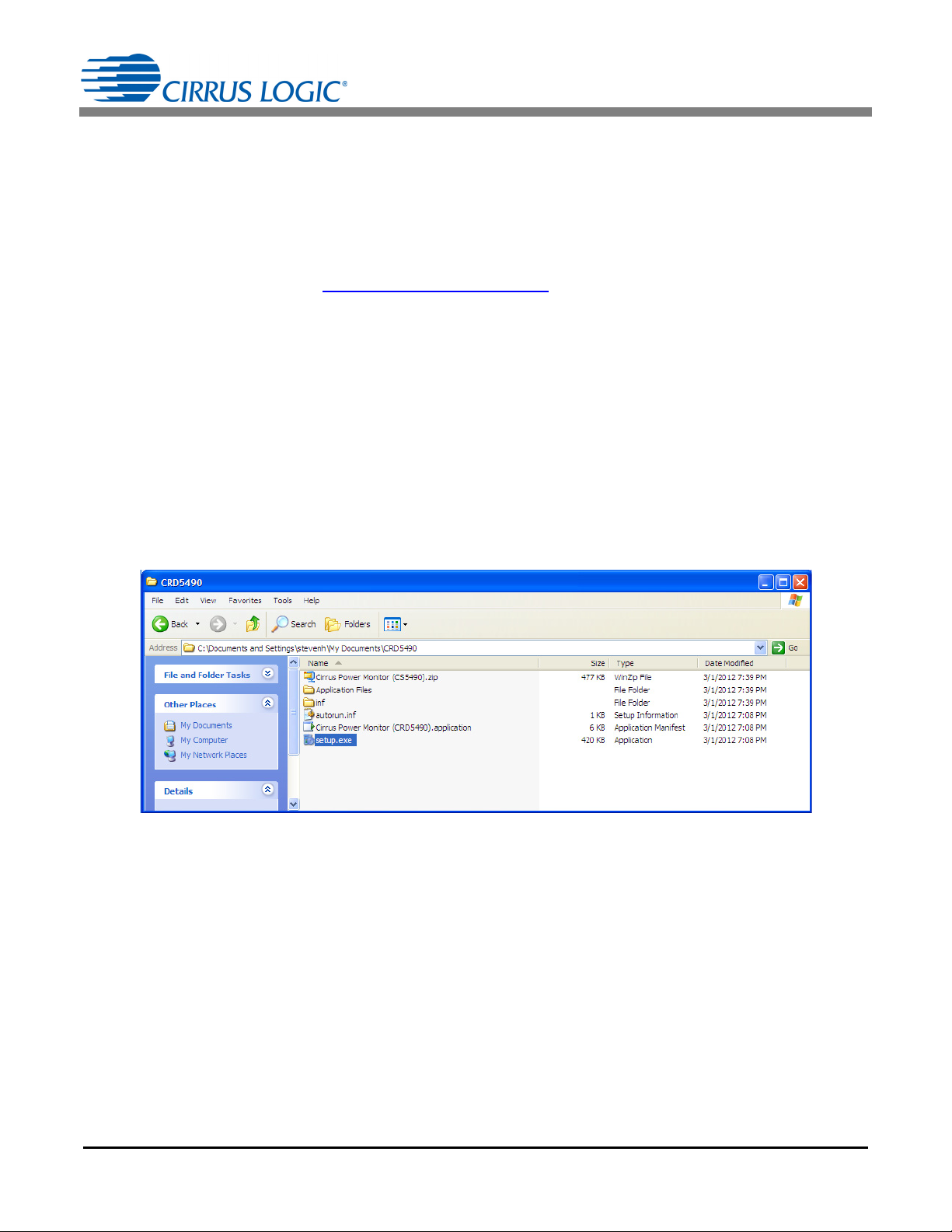
Figure 5. Location of the Unzipped Files
3. SOFTWARE OVERVIEW
The evaluation board comes with software and a USB cable to link the evaluation board to the PC. The evaluation
software was developed with Microsoft
™
7
. The following procedure is based on Windows XP.
3.1 Installation Procedure
Follow the steps below to install the GUI and the CDC driver software:
1. Access the following web site: http://www.cirrus.com/en/support
2. Click the Energy Measurement link.
3. Click the CRD5490 link. The Software License web page is displayed.
4. To agree with the terms and conditions, click the Agree button. The File Download window is displayed.
5. Click the Save button. The Save As window is displayed.
6. Select a location to store the compressed folder.
7. Click the Save button. The Download complete window is displayed.
8. Click the Open Folder button. The location where the compressed folder is stored is displayed.
9. Right-click on the compressed folder, and click Extract All.
10. Select a location to extract the files.
11. Navigate to the location where the extracted files are stored and double-click on the setup.exe file.
®
Visual Studio® and was designed to run with Windows XP™ and Windows
.
DS988RD1 7
Page 8
CRD5490-Z
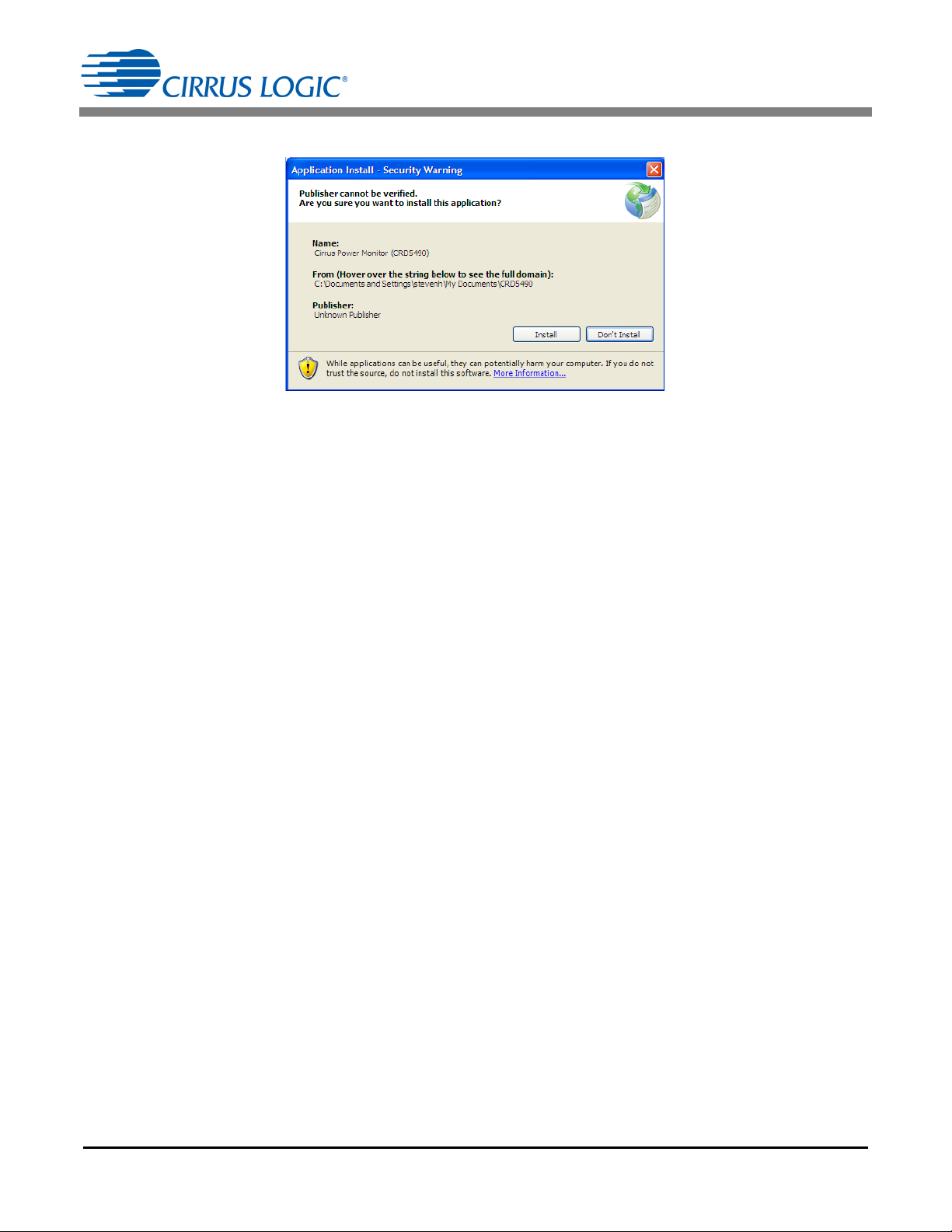
Figure 6. Application Install - Security Warning Window
The application will verify system requirements. The Application Install - Security Warning window is displayed.
12. Click the Install button.
13. Follow the instructions of the Microsoft.Net Framework installation.
The Microsoft.Net Framework may need to be installed on the system. Internet access may be required to install
the Framework or language packs. The download will start automatically. If installation stops after Framework
is installed, select setup.exe from step 11.
The installation program will automatically load the application after installation. If the CDC driver is already installed and the CRD5490-Z is connected (AC power and USB cable), then the CRD5490-Z will be recognized
and ready.
If the CDC driver is not installed, connect the USB and AC power source, then install the serial CDC Driver when
Windows recognizes the device. Refer to Appendix 2: CDC Driver Installation on page 26 for more details.
14. If necessary, execute the GUI using the next section, 3.1.1 Executing the GUI.
3.1.1 Executing the GUI
1. From the Start menu, click All Programs.
2. Click Cirrus Logic.
3. Click Cirrus Power Monitor (CS5490). The GUI is launched.
8 DS988RD1
Page 9
CRD5490-Z
WARNING
High Voltage Hazard
When the CRD5490-Z is connected to AC lines, high voltage is present inside
the box. Do not remove the protective cover from the CRD5490-Z when power is
connected.
The evaluation board connects directly to the AC power line and presents a serious risk of
electric shock and can cause serious injury or death. Extreme caution needs to be
exercised while handling this box. Make sure that the power source is off before wiring any
connection. Make sure that all connectors are well connected before the power source is
turned on. Make sure all AC power line wiring is secured to the box and away from contact
before the power source is on.
Refer to additional warnings at the beginning of this document.
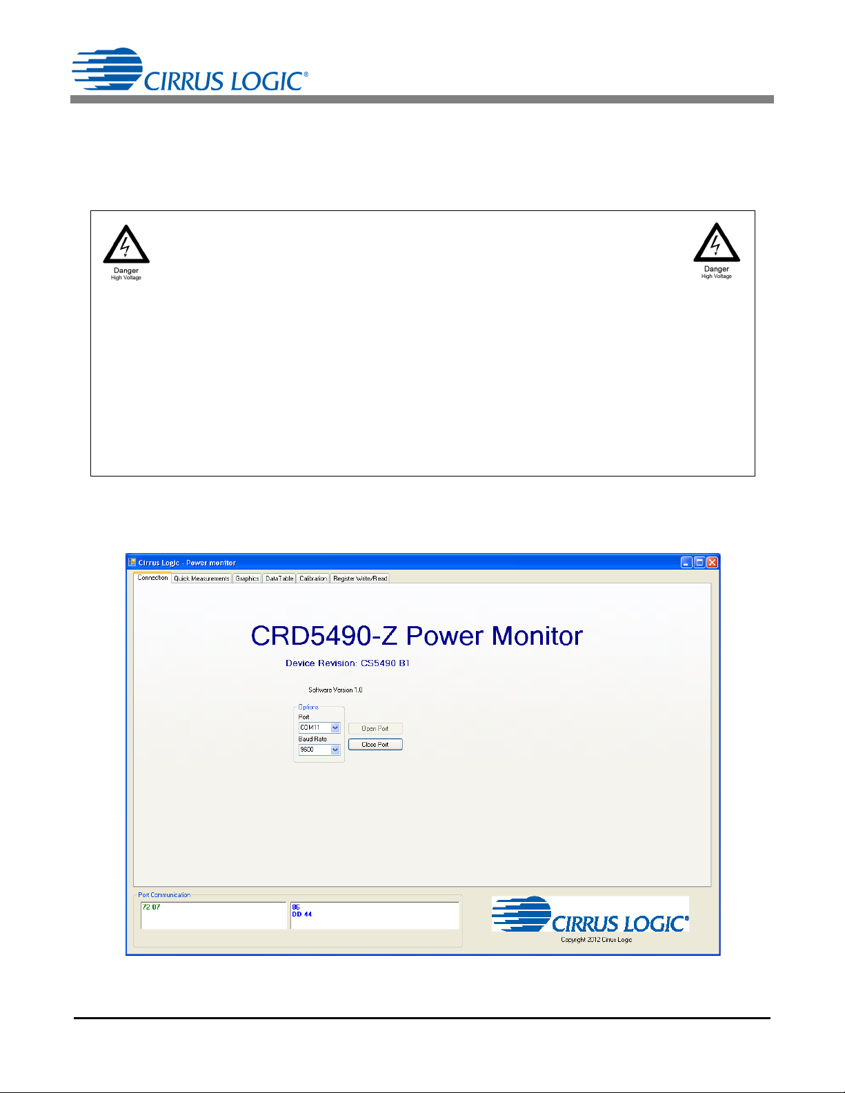
Figure 7. Cirrus Logic - Power monitor Window
3.2 Using the Software
Before launching the software, ensure that all of the cables connected to the CRD5490-Z are installed (as described
in the Hardware Overview section on page 4) and connect the board to an open USB port on the PC using the
provided cable. Once the board is powered through the AC line and USB, the software program can be launched.
3.3 Start-up Window
When the software is launched, the Cirrus Logic - Power Monitor window is displayed. This window contains
information about the software's title, version, and device revision number. See Figure 7.
The tabs in this window provide access to GUI functions. The following subsections describe the tabs in this window.
DS988RD1 9
Page 10
CRD5490-Z
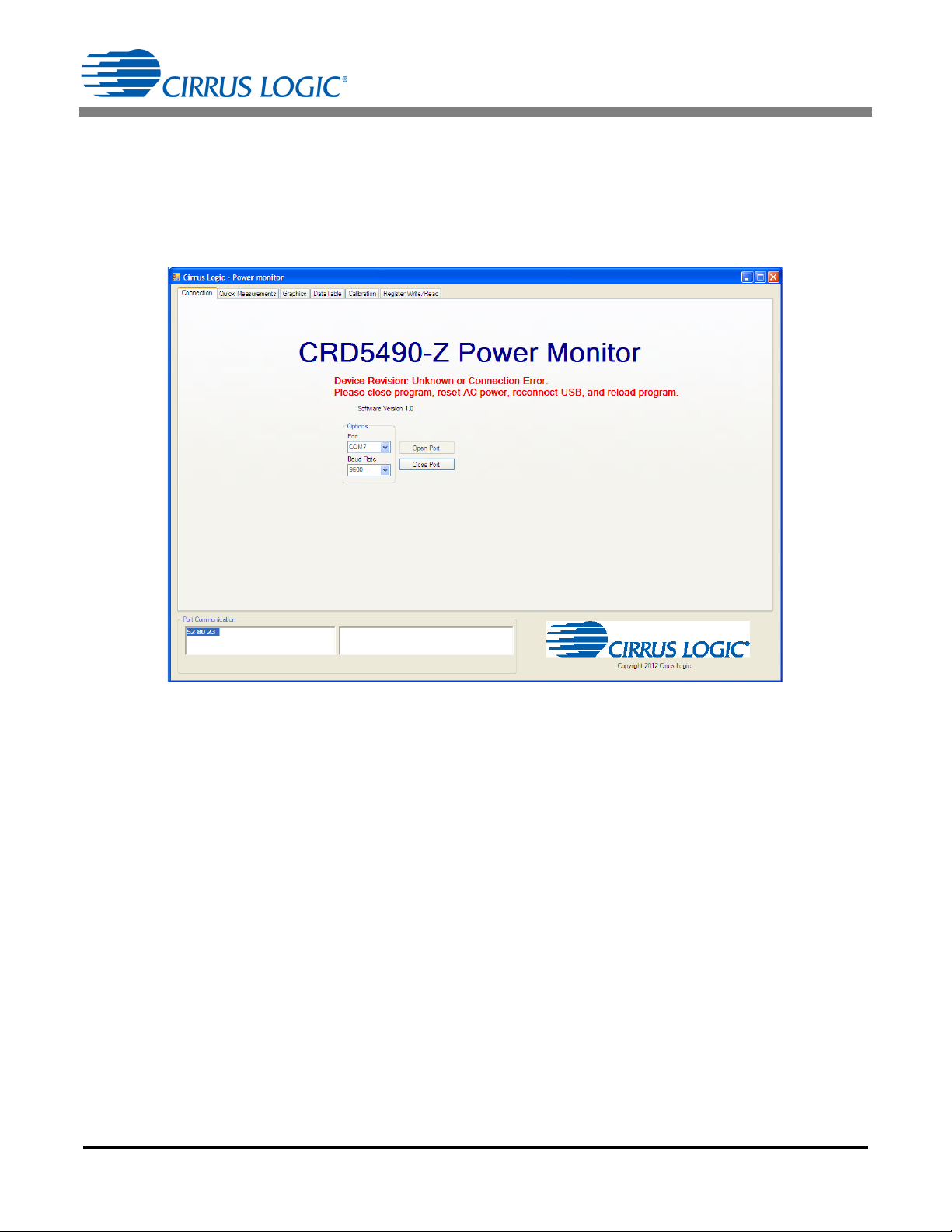
Figure 8. Connection Tab with Communication Error Displayed
3.3.1 Connection Tab
The Connection tab displays the USB communication with CRD5490-Z board. At startup, the GUI attempts to
establish a connection to the CRD5490-Z to the PC through the last USB device connected.
Once the USB communication has been established, the CS5490 serial port will report the Device Revision on the
Connection tab. If the software is unable to establish a communication link with the CRD5490-Z board, a message
is displayed indicating that the initial communication has failed. This message is displayed in Figure 8.
3.3.1.1 Common Causes of Communication Error
• No AC power
• USB cable is not connected
• USB cable to the CRD was not the last device connected before loading the GUI
• Windows is not given time to recognize the device and assign a serial port
• The wrong serial port is assigned because the GUI was loaded before the above items were met
3.3.1.2 Fixing Communication Problems
1. Close the GUI.
2. Remove the power to the CRD5490-Z by turning off the AC source.
3. Remove the power to the MCU by removing the USB cable from the PC.
4. Check that the AC power connections are secure.
5. Connect the USB cable to the PC.
6. Wait for Windows to detect the CDC Device. Verify the port by opening the Device Manager and reviewing the
port assignments (run “devmgmt.msc” at a command prompt or Windows 7 search).
7. Apply AC power and wait a second.
8. Reload the GUI.
10 DS988RD1
Page 11
CRD5490-Z
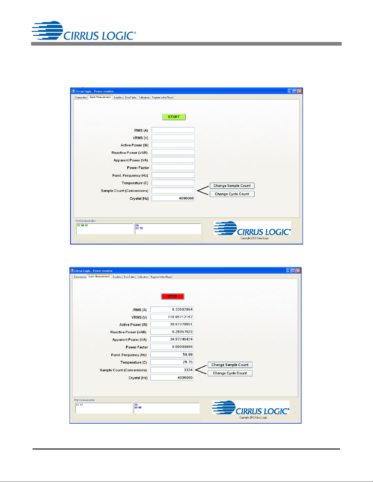
Figure 9. Quick Measurements Tab - Idle
Figure 10. Quick Measurements Tab - Continuous Convert
3.3.2 Quick Measurements Tab
The Quick Measurements tab displays reported power data from the CS5490 device in real time as continuous
conversions are performed. Refer to the CS5490 data sheet, entitled Two Channel Energy Measurement IC, for
more information about continuous conversion.
DS988RD1 11
Page 12
CRD5490-Z
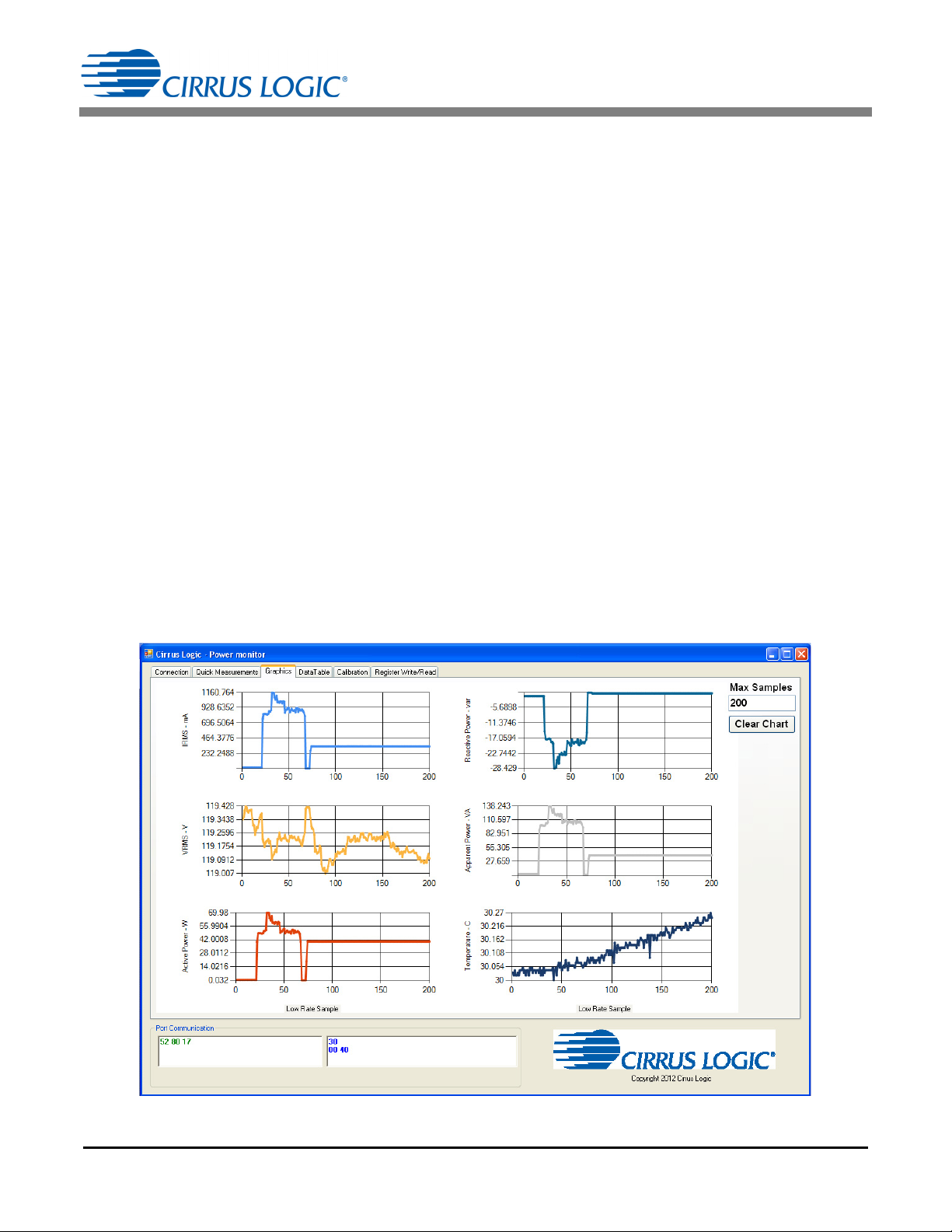
Figure 11. Graphics Tab
The Connection, Graphics, and Quick Measurements tabs may be viewed with the conversions running, but the
continuous conversions should be stopped before moving to the Data Table, Calibration, or Register Write/ Read
tabs.
3.3.2.1 START Button
The START button starts continuous conversions execution until the STOP button is clicked. The power
measurements are updated with present values in the CS5490 data registers after each conversion. The refresh
rate is configured by the SampleCount or CycleCount register.
3.3.2.2 Change Sample Count Button
Whether this option is available depends on the CS5490 device revision and configuration. The default low-rate
refresh rate for data is 1 second, or 4000 samples. Click the Change Sample Count button to change the
SampleCount register. Enter a larger number of samples to slow the low-rate refresh rate. It is not recommended to
reduce the SampleCount below 2000 samples.
3.3.2.3 Change Cycle Count Button
Whether this option is available depends on the CS5490 device revision and configuration. The default low-rate
refresh rate for data is 1 second, or 100 line cycles at 50Hz. The CS5490 counts the samples in a half-line cycle and
updates the SampleCount register automatically based on the CycleCount entered. Click the Change Cycle Count
button to change the CycleCount register. Enter a larger number of cycles to slow the low-rate refresh rate. It is not
recommended to reduce the CycleCount 50 cycles.
3.3.3 Graphics Tab
The Graphics tab displays the power data of the CS5490 versus low-rate samples in individual charts. To view data
in real time, click the START button on the Quick Measurements tab, which initiates conversions, and then click the
Graphics tab to bring it forward.
12 DS988RD1
Page 13

CRD5490-Z
Selected Chart Area
Selected Chart Area Magnied
Figure 12. Graphics Tab with Chart Zoom Example
The charts’ scales will automatically adjust for the data captured. To zoom in on a portion of a chart, click in the chart
and drag a box over the portion to be enlarged. Scroll bars are displayed in the magnified chart. See Figure 12.
It is recommended to stop conversions before clicking on charts. Transactions are stopped when selecting a chart,
and samples may be missed.
3.3.3.1 Max Samples Field
The charts will display a maximum number of samples based on the value entered in the Max Samples field. It is
recommended to stop conversions before entering new values into the Max Samples field. Changes take effect
immediately.
The Max Samples field should not be made too large. Otherwise, the window will update slowly and samples will be
missed. When using the default sample count, generally the Maximum Samples field should be less than 500
samples and may vary depending on the PC hardware. To view a larger number of samples without missing
samples, click the Quick Measurements tab to bring it forward, wait for data to be collected, stop conversions, and
then click on the Graphics tab to bring it forward.
3.3.3.2 Clear Chart Button
The Clear Chart button clears all the charts.
DS988RD1 13
Page 14

CRD5490-Z
Figure 13. Data Table Tab
3.3.4 Data Table Tab
The Data Table tab displays the CS5490 power information in a table. Stop conversions before viewing the Data
Table tab.
3.3.4.1 Write Table Button
The Write Table button writes the full data table to a comma-delimited file (*.csv) using Windows’ standard file
window. Select the directory location and filename in the Save As window.
3.3.4.2 Clear Table Button
The Clear Table button clears the table.
14 DS988RD1
Page 15

CRD5490-Z
Figure 14. Calibration Tab
Figure 15. Quick Measurements Tab with Error Message Displayed (Partially Illustrated)
3.3.5 Calibration Tab
The Calibration tab is used to write and display to the CS5490 offset and gain calibration registers. The built-in
calibration sequences of the CS5490 that are used to set the calibration register can be initiated from the Calibration
tab. AC offset and gain calibration can be performed on the voltage channel, the current channel, or both
simultaneously. Refer to the CS5490 data sheet, entitled Two Channel Energy Measurement IC, and Application
Note AN366, entitled CS5480/84/90 Energy Measurement IC Calibration, for more details on calibration. The
Calibration tab is illustrated in Figure 14.
To access the Calibration tab, conversion must be stopped. Otherwise, the Quick Measurements tab will be
displayed with the error message shown in Figure 15.
The Refresh button updates the contents of the screen by reading all the register values from the CS5490. It is
recommended to click the Refresh button when entering the Calibration tab or after modifying any registers to reflect
the current status of the CS5490.
DS988RD1 15
Page 16

CRD5490-Z
CRD5490-Z
AC
SOURCE
AC
Load
GUI
USB
Reference
Power
Meter
(V, A)
*
Figure 16. Gain Calibration Configuration
3.3.5.1 AC Offset / Gain Register
In the AC Offset and Gain fields, the AC offset and gain registers for all channels are displayed in hexadecimal
format. These registers can be modified directly by typing values in the fields and then pressing Enter on the
keyboard. The AC offset register only affects the current channel's I
3.3.5.2 Performing Calibrations
To ensure accurate results, Gain calibration should be performed before AC offset calibration. The gain calibration
can be performed on both the voltage and current channels of the CS5490. The AC offset calibration can be
performed only on the current channel. In the CS5490, the initial values in the calibration registers affect the results
of the calibration. The register values are shown in blue in Figure 14. Before calibration, the gain and offset registers
should be configured in their default state 0x 40 0000 (gain = 1) for gain registers and 0x 00 0000 (clear = 0) for
offset registers.
Gain Calibration
For gain calibration, the CRD5490-Z software configures the gain registers prior to setting up calibration based on
the reference meter readings. The CRD5490-Z software uses the non-full scale gain calibration techniques and
formulas in Appendix 3: Non-Full Scale Gain Calibration (see page 33) to set up the CS5490 voltage and current
channel gain registers before calibration. The AC offset register values are not modified by the software, and the
current configuration are used. The default AC offset register value should be 0x 00 0000.
1. Attach an AC reference meter as configured in Figure 16. It is important to use short and large gauge wires to
attach the reference power meter to reduce error.
register values.
RMS
2. Attach and turn on an AC source.
3. Attach and turn on AC load. For this example, a 200W light bulb is used, but it is recommended to use a load
that is at a minimum of ½ of the full-scale load current.
16 DS988RD1
Page 17

4. Confirm that the initial conditions are configured as shown in Figure 17:
Figure 17. Calibration Tab with Initial Calibration Configuration
CRD5490-Z
5. Click the Quick Measurements tab to bring it forward, and click the START button.
6. Wait approximately 5 to 10 seconds for the readings to update.
7. Click the STOP button.
DS988RD1 17
Page 18

CRD5490-Z
Figure 18. Calibration Tab with Reference Meter Reading
Figure 19. Calibration Tab with Confirmation Message
8. Record the reference meter measurements after the setup has settled and before calibration is executed. See
Figure 18.
9. Click the Gain Calibration button.
10. A confirmation message is displayed, as shown in Figure 19.
18 DS988RD1
Page 19

CRD5490-Z
Figure 20. Calibration Tab with Gain Register Updated After Gain Calibration
Figure 21. Quick Measurements Tab Showing Results that Should Match the Reference Meter
If the calibration conditions (voltage and current) match the reference meter readings, click the Yes button.
11. The gain register values automatically update when the calibration is complete.
12. To confirm results click the Quick Measurements tab to bring it forward, and click the START button.
13. Results should match the reference meter readings.
DS988RD1 19
Page 20

CRD5490-Z
Figure 22. Quick Measurements Tab - Note I
RMS
before AC Offset Calibration
AC Offset Calibrations
For AC offset calibration, the CRD5490-Z software clears the offset register before calibration begins. The gain
register values are not modified by the software, and the current configuration is used from the prior gain calibration.
AC calibration only affects the current channel's I
1. Continue from step 13 in the Gain Calibration section on page 16 and keep the AC source on.
2. Remove the AC load.
3. Open the Quick Measurements tab and click the START button.
4. Wait approximately 5 to 10 seconds for readings to update.
5. Click the STOP button.
6. Confirm that the current is as expected during a no-load condition. Inspect the pre-calibrated I
RMS
value.
RMS
closely.
7. Click the Calibration tab to bring it forward, and click the AC Offset Calibration button.
20 DS988RD1
Page 21

8.
Figure 23. Calibration Tab with CONFIRM LOAD Window
Figure 24. AC Offset Register Updated After AC Offset Calibration
Confirm the load has been removed or turned off, and then click
Figure 23.
CRD5490-Z
Yes
from the CONFIRM LOAD window shown
in
9. The offset register value automatically updates when the calibration is completed (approximately 5 seconds).
The AC Offset register value should change.
DS988RD1 21
Page 22

CRD5490-Z
Figure 25. Confirm I
RMS
Reduced After AC Offset Calibration
10. To confirm results, click the Quick Measurements tab to bring it forward, and click the START button.
Results should show a reduction in the I
value without the load.
RMS
22 DS988RD1
Page 23

3.3.6 Register Write/Read Tab
Figure 26. Register Write/Read Tab - Read
The Register Write/Read tab allows access to the CS5490 registers directly. See Figure 26.
CRD5490-Z
There are two types of transactions: Write and Read. The CS5490 memory is organized by pages. In order to
properly write a register, it is necessary to set the Page, Address, and Data field and then click the Write button. To
read a register it is necessary to set the Page and Address and then click the Read button. Figure 26 shows the read
operation. The serial port traffic can be seen in the bottom left corner. The register result is displayed in the Data
Write/Read (hex) field. Refer to the CS5490 data sheet, entitled Two Channel Energy Measurement IC, for more
details on registers and commands. Note that the write data in the Port Communication field has an extra leading
command byte - “52” in the example. This is a read command for the MCU. Read data does not contain an extra byte.
Common CS5490 registers can be written to a file using the SAVE button in the Device Configuration panel. The
LOAD button is used to recall the common CS5490 registers that were previously saved. It is recommended to
configure the device using the Write button, start conversions from the Quick Measurements tab, stop conversions,
and then save the current configuration to a file.
DS988RD1 23
Page 24

4. REVISION HISTORY
Revision Date Changes
RD1 APR 2012 Initial Release.
CRD5490-Z
24 DS988RD1
Page 25

APPENDIX 1: CRD5490 GUI REMOVAL
Figure 27. Control Panel Window
Figure 28. Add or Remove Programs with Cirrus Power Monitor (CRD5490) Displayed
Follow the steps below to remove the CS5490 GUI software:
1. From the Start menu, click Control Panel. The Control Panel window is displayed.
CRD5490-Z
2. Click Add or Remove Programs. The Add or Remove Programs window is displayed.
3. Highlight to select the Cirrus Power Monitor (CRD5490) item, as shown in Figure 28.
4. Click the Change/Remove button, and follow the instructions. The CS5490 GUI is removed.
DS988RD1 25
Page 26

CRD5490-Z
Figure 29. Start Menu with Drivers and Printers Selected
APPENDIX 2: CDC DRIVER INSTALLATION
This Appendix includes the procedures for installing the CDC driver for both Windows 7 and Windows XP.
2.1 Installing the CDC Driver Using Windows 7
Follow the instructions below to install the CDC driver on the Windows 7 operating system.
1. Connect the provided USB cable from the CRD5490-Z to the PC. Windows will recognize the device.
2. From the Start menu, select Devices and Printers.
3. Right-click the CDC RS-232 Emulation Demo icon.
The CDC RS-232 Emulation Demo Properties Window is displayed.
4. Click the Hardware tab to bring it forward.
26 DS988RD1
Page 27

5. Click the Properties button
Figure 30. CDC RS-232 Emulation Demo Properties Window
Figure 31. General Tab with the Change Settings Button Highlighted
CRD5490-Z
6. Click the General tab to bring it forward, and click the Change Settings button.
DS988RD1 27
Page 28

7. Click the Update Driver button.
Figure 32. General Tab with the Update Driver Button Active
Figure 33. Update Driver Software Panel Options (Partially Illustrated)
CRD5490-Z
The Update Driver Software CDC RS-232 Emulation Demo panel is displayed.
8. Click Browse my computer for driver software.
9. Select the extracted file location, then select the. \inf\win2K_winxp\ directory.
28 DS988RD1
Page 29

10. Follow the installation instructions. If warnings are displayed, select to continue anyway.
Figure 34. Windows Security Warning
Figure 35. Pop-up Menu
CRD5490-Z
11. Right-click the device. A pop-up menu is displayed.
DS988RD1 29
Page 30

12. Click Properties. The Communications Port (COM3) Properties window is displayed.
Figure 36. Communications Port (COM3) Properties Window
Figure 37. Found New Hardware Wizard Window
CRD5490-Z
The next time this device is used, it will be recognized, and installing the driver will not be necessary.
2.2 Installing the CDC Driver Using Windows XP
Follow the instructions below to install the CDC driver on the Windows XP operating system.
1. Connect the provided USB cable from the CRD5490-Z to the PC. Windows XP recognizes the device, and the
Found New Hardware Wizard opens. Select to install from a specific location.
30 DS988RD1
Page 31

CRD5490-Z
Figure 38. Browse For Folder Window
Figure 39. Found New Hardware Wizard
Window Showing Files Being Transferred
2. Locate the driver information file provided with the software installation and browse to the driver file:
\ inf \ win2K_winxp \
3. Click the OK button.
4. Click the Next and follow the instructions. If warnings are displayed, select to continue.
DS988RD1 31
Page 32

5. When the installation is complete, click the Finish button.
Figure 40. Found New Hardware Wizard Window
with a Message that Installation Is Complete
CRD5490-Z
The next time this device is used on the computer, it will be recognized, and the installation of the driver will not
be necessary.
32 DS988RD1
Page 33

CRD5490-Z
V
GAIN pre
V
MAX
V
REF
-------------- -
2
22
=
[Eq: 1]
I
GAIN pre
I
MAX
I
REF
------------
2
22
=
[Eq: 2]
APPENDIX 3: NON-FULL SCALE GAIN CALIBRATION
When resources are limited, it may be necessary to provide non-full-scale amplitudes and perform built-in
calibration. To perform a non-full-scale calibration, the initial gain register conditions of the device must be identified
before calibration. Usually, initial gain register conditions are set to a default value of one, but this is not required.
Instead, the initial gain register conditions are set to accommodate the non-full-scale input calibration. Before
calibration is executed, the gain register can be set using the following equations:
where:
V
GAIN(pre)
I
GAIN(pre)
V
MAX
I
MAX
V
REF
Value stored in voltage gain register (page 16, address 35) before calibration starts
Value stored in current gain register (page 16, address 33) before calibration starts
Maximum voltage of the meter defined by customer
Maximum current of the meter defined by customer
Voltage of the line just before calibration as measured with reference meter assumes
stable input
I
REF
Load current just before calibration as measured with reference meter assumes stable
input
Follow the steps below to perform a non-full-scale gain calibration:
1. Set the line voltage and load current V
2. Confirm that the reference meter shows V
3. Set V
GAIN(pre)
per Equation 1 and I
GAIN(pre)
and I
REF
REF
REF
and I
per Equation 2.
, respectively.
of the input.
REF
4. Send the calibration command.
5. After calibration, the meter will be adjusted for a full-scale voltage of V
suring the V
REF
and I
measurements.
REF
MAX
and I
and will currently be mea-
MAX
Reference Limits
The calibration line voltage (V
) or load current (I
REF
) must not be set too low. It is recommended to keep the
REF
register values at a minimum of ½ of the maximum levels. Since the gain register can be set to a maximum value of
4, the input could be set to ¼ of the maximum levels. It is not recommended to set the input to ¼ of the maximum
levels due to variations in setup conditions. If the input is too low, the gain register will set the default value of one
after calibration.
DS988RD1 33
Page 34

CRD5490-Z
I
SCALE
I
REF
I
MAX
------------
0.6 2
23
=
[Eq: 3]
Current Scale Register
To perform calibration with less than full scale load without using the above procedure, it is possible to set the current
channel's Scale register. The current channel calibration data path contains a Scale register (page 18, address 63)
that can be adjusted before calibration to accommodate the non-full-scale load.
where:
I
SCALE
I
MAX
I
REF
Value stored in the SCALE register before calibration
Maximum current of the meter defined by the customer
Load current before calibration, as measured with a reference meter, assuming stable
input
Follow the steps below to set the current channel’s Scale register.
1. Set the load current, I
2. Confirm that the reference meter shows V
3. Set I
per Equation 3.
SCALE
(assuming V
REF
is set to full scale).
REF
and I
REF
REF
of the input.
4. Send the calibration command.
5. After calibration, the meter will be adjusted for a full-scale voltage of V
suring the V
REF
and I
measurements.
REF
MAX
and I
MAX
6. The Scale register is not in the normal data path but instead in the calibration path.
and will currently be mea-
34 DS988RD1
Page 35

DS988RD1 35
4. SCHEMATIC
CRD5490-Z
Page 36

36 DS988RD1
NMC0603X7R104K16TR
PF
(
@
Figure 41. Bill of Materials (Page 1 of 2)
5. BILL OF MATERIALS
BOM#: 505-00554-Z1 Rev: A2 BOM Desc: PWA CRD5490-Z-NPb
Date Generated: 03/21/2012
Line Item
Part
Cirrus PN
Ass
0001 P 011-00068-Z1 A CAP 0.33uF ±10% 310V MTL FLM NPb TH A 1 EA C1
0002 P 011-00051-Z1 A CAP 10nF ±20% 440V MTL FLM NPb TH A 1 EA C2
0003 P 012-00198-Z1 A CAP 100uF ±20% 50V ELE NPb RAD 8X12 A 1 EA C3
0004 P 001-02189-Z1 A CAP 0.1uF ±10% 16V X7R NPb 0603 A 7 EA C4 C7 C 9 C10 C11 C21 C25
0005 P 001-01997-Z1 A CAP 0.01uF ±10% 25V X7R NPb 0603 A 1 EA C5
0006 P 004-00068-Z1 A CAP 4.7uF ±10% 10V NPb TANT CASE A A 1 EA C6
0007 P 001-10127-Z1 A CAP 22pF ±10% 50V C0G NPb 0603 A 1 EA C8
0008 P 001-02068-Z1 A CAP 0.022uF ±10% 50V X7R NPb 0603 A 2 EA C12 C13
0009 P 001-01621-Z1 A CAP 220pF ±5% 50V X7R NPb 0603 A 4 EA C14 C15 C19 C20
0010 P 001-10048-Z1 A CAP 22pF ±5% 50V C0G NPb 0603 A 1 EA C16
0011 P 001-02780-Z1 A CAP 22pF ±10% 50V C0G NPb 0805 A 1 EA C17
0012 P 001-10193-Z1 A CAP 2.2uF ±10% 10V X7R NPb 0805 A 1 EA C18
0013 P 001-01937-Z1 A CAP 4700pF ±10% 50V X7R NPb 0603 A 1 EA C22
0014 P 012-00212-Z1 A CAP 680uF ±20% 10V ELEC NPb CASE F A 1 EA C23
0015 P 001-10152-Z1 A CAP 1uF ±10% 50V X7R NPb 1206 A 1 EA C26
0016 P 001-10192-Z1 A CAP 0.47uF ±10% 10V X5R NPb 0603 A 1 EA C27
0017 P 070-00173-Z1 A DIODE RECT 1A 400V NPb SMB A 1 EA D1
0018 P 070-00055-Z1 A DIODE ARRAY 5V
0019 P 165-00060-Z1 A LED BLU 470nm 5mA 45MCD NPb 0603 A 1 EA D3
0020 P 110-00340-Z1 A CON TERM .11PCB TAB NPb TH A 4 EA E1 E2 E3 E4
0021 P 303-00008-Z1 A FUSE CLIP PC MOUNT 5MM NPb A 2 EA F1
0023 P 115-00162-Z1 A HDR 6x1 ML .1"CTR 062 S GLD NPb TH A 1 EA J1
0024 P 115-00258-Z1 A HDR 4x2 ML .1" 093BD ST GLD NPb TH A 1 EA J2
0025 P 110-00263-Z1 A CON USB RCPT RA 5POS MINI-B NPb TH A 1 EA J3
0026 P 145-00040-Z1 A FE 1.5A 80 ohm
0027 P 040-00149-Z1 A IND 1000uH ±10% 300mA NPb RAD A 1 EA L2
0028 P 304-00004-Z1 A SPCR STANDOFF 4-40 THR .500"L NPb A 0 EA MH1 MH2 MH3 MH4
0029 P 071-00046-Z1 A TRAN SIG NPN 40V 0.2A NPb TO-92 A 1 EA Q1
Rev Description Status Qty UM Ref Desg Man'f Man'f PN ECO Effective Date Notes LTime
TVS) ESD NPb SOT143 A 1 EA D2
100MHz NPb 0805 A 1 EA L1
BC COMPONENTS BFC233912334
BC COMPONENTS BFC233814103
UNITED CHEMI-CON ELXZ500ELL101MH12D
KEMET
KOA
VENKEL
PANASONIC
NIC COMPONENTS
WALSIN
KEMET
KOA
PANASONIC
KEMET
VENKEL
AVX
KEMET
WALSIN
KEMET
PANASONIC
KEMET
KOA
PANASONIC
NIC COMPONENTS
PANASONIC
WALSIN
KEMET
KOA
PANASONIC
KEMET C0805C225K8RAC
KEMET
PANASONIC
WALSIN
PANASONIC EEEFK1A681P
TDK C3216X7R1H105K
KEMET
WALSIN
DIODES INC S1GB-13-F
LITTELFUSE SP0503BAHTG
OSRAM LB Q39G-L2N2-35-1
TYCO 61968-1
KEYSTONE 3517
SAMTEC TSW-106-07-G-S
SAMTEC
TONGYUEQING
MOLEX 54819-0519
STEWARD MI0805K400R-10
BOURNS RLB0914-102KL
KEYSTONE
JIAXINGLONG
FAIRCHILD
SEMICONDUCTOR
C0603C104K4RAC
X7R0603CTTD104K
C0603X7R160-104KNE
ECJ1VB1C104K
0603B104K160CT
C0603C103K3RAC
X7R0603ETTD103K
ECJ1VB1E103K
T491A475K010AT
TA010TCM475KAR
TAJA475K010R
C0603C220K5GAC
0603N220K500LT
C0603C223K5RAC
ECJ1VB1H223K
C0603C221J5RAC
X7R0603HTTD221J
ECJ1VB1H221J
NMC0603NPO220J50TR
PF ECJ1VC1H220J
0603N220J500LT
C0805C220K5GAC
NPO0805HTTD220K
ECJ2VC1H220K
C0603C472K5RAC
ECJ1VB1H472K
0603B472K500CT
C0603C474K8PAC
0603X474K100CT
TSW-104-08-G-D
PHED-DS008G1ABONA
2203
M3X13
2N3904
ECO922 0
ECO937 7
ECO922 SEE
ECO922 SEE
ECO922 NO POP 7
COMMENTS
COMMENTS
89.999
19.999
7
7
7
7
7
7
7
7
7
7
7
7
7
7
7
7
0
7
7
7
7
7
7
CRD5490-Z
Page 37

DS988RD1 37
p
NMC0603X7R104K16TR
PF
Figure 42. Bill of Materials (Page 2 of 2)
BOM#: 505-00554-Z1 Rev: A2 BOM Desc: PWA CRD5490-Z-NPb
Date Generated: 03/21/2012
Line Item
Part
Cirrus PN
Ass
0030 P 031-00054-Z1 A RES 270 OHM 3W ±5% MTL FLM NPb AXL P 1 EA R1
0031 P 020-06493-Z1 A RES 0.002 OHM 2W ±1% NPb 2512 A 1 EA R2
0032 P 020-06362-Z1 A RES 422k OHM 1/4W ± 1% NPb 1206 A 4 EA R3 R4 R5 R6
0033 P 020-01016-Z1 A RES 1k OHM 1/10W ± 1% NPb 0603 FILM A 7 EA R7 R8 R9 R10 R11 R15 R21
0034 P 021-00238-Z1 A RES 680 OHM 1/10W ±5% NPb 0603 FILM A 1 EA R12
0035 P 021-00258-Z1 A RES 4.7k OHM 1/10W ±5% NPb 0603 FLM A 3 E A R13 R14 R16
0036 P 021-00259-Z1 A RES 5.1k OHM 1/10W ±5% NPb 0603 FIL A 2 EA R17 R19
0037 P 021-00253-Z1 A RES 3k OHM 1/10W ±5% NP b 0603 FILM A 1 EA R18
0038 P 021-00292-Z1 A RES 120k OHM 1/10W ± 5% NPb 0603 FIL A 2 EA R20 R25
0039 P 020-00673-Z1 A RES 0 OHM 1/10W ±5% NPb 0603 FILM A 3 EA R22 R27 R28
0040 P 031-00070-Z1 A RES 1M OHM 1/2W ±5% CF NPb AXL A 1 EA R23
0041 P 021-00218-Z1 A RES 100 OHM 1/10W ±5% NPb 0603 FILM A 1 EA R24
0042 P 021-00294-Z1 A RES 150k OHM 1/10W ± 5% NPb 0603 A 1 EA R26
0043 P 110-00045-Z1 A CON TEST PT .1"CTR TIN PLAT NPb BLK A 3 EA TP1 TP3 TP4
0044 P 175-00030-Z1 A OPT COUPLER PHOTOTRANS NPb DIP4 A 3 EA U2 U5 U6
0045 P 065-00334-Z3 B0 IC CRUS ENER MEAS NPb SOIC16L I 1 EA U4
0046 P 062-00242-Z1 A IC MCU 8b FLASH 768kx16 NPb QFN20 A 1 EA U7
0047 P 060-00614-Z1 A IC CONV SW BUCK 0.5A NPb SOIC8 A 1 EA U8
0048 P 036-00018-Z1 A VARISTOR 275Vrms 10MM NPb RAD A 1 EA VR1
0049 P 300-00004-Z1 A SCREW 4-40X1/4"L PH STEEL NPb A 0 EA XMH1 XMH2 XMH3 XMH4
0050 P 100-00132-Z1 A XTL 4.096MHZ 30ppm 18pF NPb SMD A 1 EA Y1
0051 P 100-00134-Z1 A XTL 12.0MHZ 18
0052 P 070-00209-Z1 A DIODE ZEN 36V 1W 5% NPb SMA A 1 EA Z1
0053 P 070-00210-Z1 A DIODE SCHOTTKY 40V 1A NPb SOD123 A 1 EA Z3
0054 P 240-00554-Z1 A PCB CRD5490-Z-NPb A 1 EA
0055 P 603-00554-Z1 A1 ASSY DWG CRD5490-Z-NPb A 1 REF
0056 P 600-00554-Z1 A2 SCHEM CRD5490-Z-NPb A 1 REF
0057 A 422-00013-Z1 D LBL SUBASSY PRODUCT ID AND REV A 1 EA
0058 P 180-00024-Z1 A FUSE 16A 250V TLAG NPb 5x20MM A 1 EA ZZ5
0059 P 001-02189-Z1 A CAP 0.1uF ±10% 16V X7R NPb 0603 A 0 EA C24
Rev Description Status Qty UM Ref Desg Man'f Man'f PN ECO Effective Date Notes LTime
f 30p NPb HC49/US SM A 1 EA Y2
PANASONIC ERG3SJ271
STACKPOLE ELECTRONICS CSNL2512FT2L00
DALE CRCW1206422KFKEA
DALE
KOA
WALSIN
KOA
NIC COMPONENTS
DALE
PANASONIC
DALE
VENKEL
PANASONIC
NIC COMPONENTS
YAGEO
WALSIN
DALE
KOA
PANASONIC
WALSIN
DALE
PANASONIC
DALE
NIC COMPONENTS
KOA
PANASONIC
DALE
NIC COMPONENTS
PANASONIC
VENKEL
WALSIN
STACKPOLE CFM12JT1M00
DALE
KOA
YAGEO
NIC COMPONENTS
PANASONIC
WALSIN
DALE
KOA
PANASONIC
KEYSTONE
CGG
VISHAY SFH610A-3
CIRRUS LOGIC CS5490-ISZ/B0
MICROCHIP PIC18F14K50-I/MQ
ON SEMICONDUCTOR LM2594DADJR2G
EPCOS
EPCOS
McMASTER-CARR 90190A106
ABRACON ABLS2-4.096MHZ-D4Y-
CTS ATS120BSM-1
TAIWAN SEMICONDUCTOR 1SMA4753
DIODES INC 1N5819HW-7-F
CIRRUS LOGIC 240-00554-Z1
CIRRUS LOGIC 603-00554-Z1
CIRRUS LOGIC 600-00554-Z1
CIRRUS LOGIC 422-00013-01
SCHURTER INC 0034.3129
KEMET
KOA
VENKEL
PANASONIC
NIC COMPONENTS
WALSIN
CRCW06031K00FKEA
RK73H1JTTD1001F
WR06X1001FTL
RK73B1JTTD681J
NRC06J681TRF
CRCW0603680RJNEA
ERJ3GEYJ681V
CRCW06034K70JNEA
CR0603-10W-472JT
ERJ3GEYJ472V
NRC06J472TRF
9C06031A4701JLHFT
WR06X472JTL
CRCW06035K10JNEA
RK73B1JTTD512J
ERJ3GEYJ512V
WR06X512JTL
CRCW06033K00JNEA
ERJ3GEYJ302V
CRCW0603120KJNEA
NRC06J124TRF
RK73B1JTTD124J
ERJ3GEYJ124V
CRCW06030000Z0EA
NRC0606ZOTRF
ERJ3EKF0R00V
CR0603-10W-000T
WR06X000PTL
CRCW0603100RJNEA
RK73B1JTTD101J
9C06031A1000JLHFT
NRC06J101TRF
ERJ3GEYJ101V
WR06X101JTL
CRCW0603150KJNEA
RK73B1JTTD154J
ERJ3GEYJ154V
5001
TP-105(BLK)
B72210S2271K101
S10K275E2
T
C0603C104K4RAC
X7R0603CTTD104K
C0603X7R160-104KNE
ECJ1VB1C104K
0603B104K160CT
30.002
ECO937 ALT LINE 60 7
ECO922 NO POP 7
ECO922 7
ECO922/937 7
ECO922 NO POP 0
7
7
7
7
7
7
7
7
7
7
7
7
7
7
7
7
7
7
7
7
0
7
0
7
CRD5490-Z
Page 38

38 DS988RD1
Figure 43. Top Routing
6. LAYOUT
CRD5490-Z
Page 39

DS988RD1 39
Figure 44. Bottom Routing
CRD5490-Z
Page 40

40 DS988RD1
Figure 45. Silkscreen
CRD5490-Z
 Loading...