

Page 1
R1
R2
R
cs
8 1
Boost Diode
Boost
FET
CS1501
CS1601
GDZCD
IFB
GND
CSIAC
VDD
L
B
6
3
57
4
V
DD
STBY
2
V
rect
V
link
33pF
AN356
Application Note
CS1501 & CS1601:
DRIVING THE ZCD PIN FROM THE MOSFET DRAIN
1. Introduction
The CS1601 is designed with ZCD (zero-current detection), providing the controller with the capability to turn on the MOSF ET
when the current through the boost inductor is close to zero. This can also be described as valley/zero crossings switching. This
is implemented by adding a sense winding on the PFC choke to detect the current.
If the addition of an auxiliary winding on the boost inductor is a problem due to design or manufacturing constraints, an alternative
method for implementing this function is presented below.
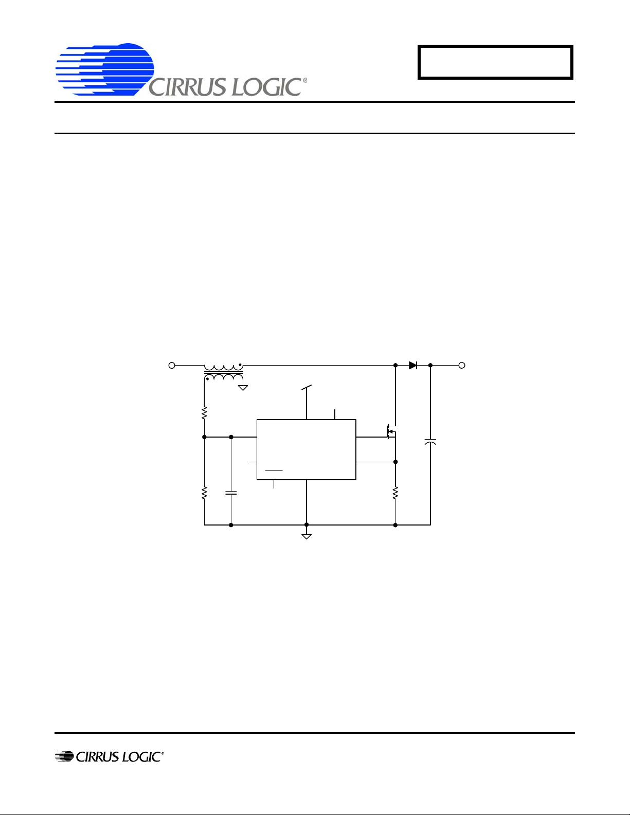
2. Standard ZCD Configuration
The standard configuration for the CS1501 & CS1601 is an auxiliary winding is added to the PFC boost inductor to provide zerocurrent detection (ZCD) information.
Figure 1. ZCD Using Auxiliary Winding on PFC Boost Inductor
An auxiliary winding is added to the PFC boost inductor to provide zero-current detection (ZCD) information. The ZCD comparator looks for the zero crossing on the auxiliary winding and switches when th e auxilia ry voltage is be low zero. Switching in t he
valley of the oscillation minimizes the switching losses and reduces EMI noise.
For a full description of ZCD operation, see the CS1501 & CS1601 data sheets.
http://www.cirrus.com
Copyright Cirrus Logic, Inc. 2011
(All Rights Reserved)
APR ‘11
AN356REV1
Page 2
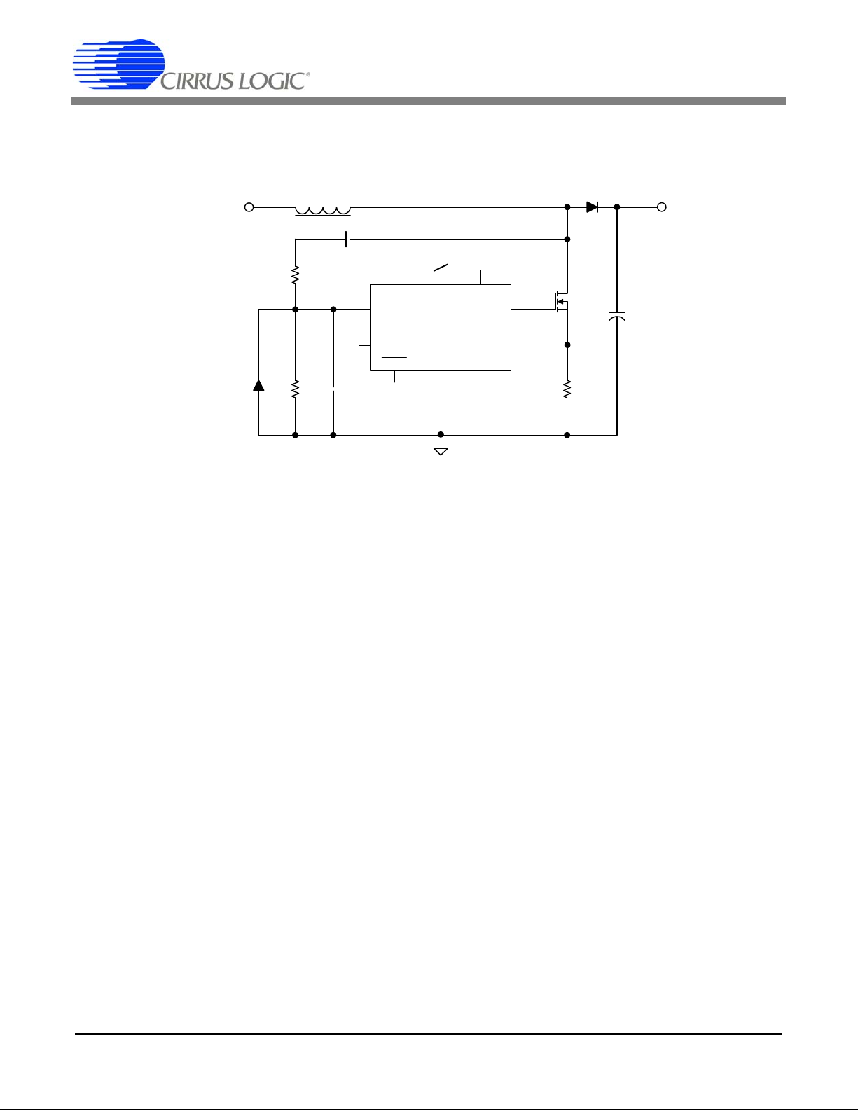
3. Alternative Configuration
R1
R2
R
cs
8 1
Boost Diode
Boost
FET
CS1501
CS1601
GDZCD
IFB
GND
CSIAC
VDD
L
B
6
3
57
4
V
DD
STBY
2
V
rect
V
link
33pF
47pF
500 V
Low Voltage
Schottky
R1
V
drainVzcd
–()
I
zcd
-------------------------------------
455kΩ==
[Eq.1]
R2
V
drain
V
zcd
–()
R1
-------------------------------------
V
zcd
⋅ 4.79kΩ==
[Eq.2]
It is possible to implement ZCD with a resistor divider from the drain of the PFC MOSFET. See Figure 2.
AN356
Figure 2. ZCD Alternative Implementation
At lighter loads, the resistor divider circuit may not pull the ZCD pin to its trigger threshold (low) as the ringing voltage itself drifts
away from zero volts. This can cause the drive to turn on while there is still a voltage across the drain to source of the Boost
MOSFET. Using a 47 pF capacitor in series with resistor R1, the issue of DC drift on the drain w aveform is remove d. The value
of the capacitor is minimized to prevent additional capacitive switching losses.
3.1 Resistor Configuration
The maximum current that can be drawn by the ZCD pin is I
on the MOSFET drain = 460 V.
Select R1 to be a standard value of 475 kΩ.
Select R2 to be a standard value of 4.75 kΩ.
Due to internal comparator design, the maximum external capacitor is 33 pF, as shown. This acts as a low-pass filter for high-
frequency switching noise. Values above this should not be used.
The addition of a Schottky diode is required to prevent negative voltages on the ZCD pin from exceeding -0.5 V. See Fig 3.
= 1mA. Set a maximum voltage of 5 V for V
zcd
, with the voltage
zcd
2 AN356REV1
Page 3

AN356
Ch 1 - MOSFET Drain
Ch 2 - ZCD Pin 5
Ch 3 - Gate Drive
Ch 4 - Current in Boost
Inductor
Ch 1 - MOSFET Drain
Ch 2 - ZCD Pin 5
Ch 3 - Gate Drive
Ch 4 - Current in Boost
Inductor
Figure 3. ZCD Performance — Operation at 100% Load, 108 VAC
Figure 4. ZCD Performance — Operation at 50% Load, 108 VAC
4. Summary
An alternative for ZCD sensing using a resistive divider is presented. Care must be taken to choose appropriate resistor value to
prevent the IC from being damaged by excessive voltages or currents.
AN356REV1 3
Page 4

5. Revision History
Contacting Cirrus Logic Support
For all product questions and inquiries contact a Cirrus Logic Sales Representative.
To find one nearest you go to http://www.cirrus.com
IMPORTANT NOTICE
Cirrus Logic, Inc. and its subsidiaries ("Cirrus") believe that the information contained in this document is accurate and reliable. However, the information is subject
to change without notice and is provided "AS IS" without warranty of any kind (express or implied). Customers are advised to obtain the latest version of relevant
information to verify, before placing orders, that information being relied on is current and complete. All products are sold subject to the terms and conditions of sale
supplied at the time of order acknowle dgment, including tho se pertaining to warra nty, indemnification, and l imitation of liability. No responsibility is assumed by Cirrus
for the use of this information, including use of this inform ation a s the basis for m anufactur e or sale of an y items, or for infringement of patents or other rights of third
parties. This document is the property of Cirrus and by furnishing this information, Cirrus grants no license, express or implied under any patents, mask work rights,
copyrights, trademarks, trade secrets or other intellectual pro perty rights. Cirrus owns the copyr ights associated with the information con tained herein a nd gives consent for copies to be made of the information only for use within your organiza tion with resp ect to Cirrus inte grated circu its or other products of Cirrus. This consent
does not extend to other copying such as copying for general distribution, advertising or promotional purposes, or for creating any work for resale.
CERTAIN APPLICATIONS USING SEMICONDUCTOR PRODUCTS MAY INVOLVE POTENTIAL RISKS OF DEATH, PERSONAL INJURY, OR SEVERE PROPERTY OR ENVIRONMENTAL DAMAGE ("CRITICAL APPLICATIONS"). CIRRUS PRODUCTS ARE NOT DESIGNED, AUTHORIZED OR WARRANTED FOR USE
IN PRODUCTS SURGICALLY IMPLANTED INTO THE BODY, AUTOMOTIVE SAFETY OR SECU RITY DEVICES, LIFE SUPPOR T PRODUCTS OR OTHE R CRITICAL APPLICATIONS. INCLUSION OF CIRRUS PRODUCTS IN SUCH APPLICATIONS IS UNDERSTOOD TO BE FULLY AT THE CUSTOMER'S RISK AND
CIRRUS DISCLAIMS AND MAKES NO WARRANTY, EXPRESS, STATUTORY OR IMPLIED, INCLUDING THE IMPLIED WARRANTIES OF MERCHANTABILITY
AND FITNESS FOR PARTICULAR PURPOSE, WITH REGARD TO ANY CIRRUS PRODUCT THAT IS USED IN SUCH A MANNER. IF THE CUSTOMER OR
CUSTOMER'S CUSTOMER USES OR PERMITS THE USE OF CIRRUS PRODUCTS IN CRITICAL APPLICATIONS, CUSTOMER AGREES, BY SUCH USE, TO
FULLY INDEMNIFY CIRRUS, ITS OFFICERS, DIRECTORS, EMPLOYEES, DISTRIBUTORS AND OTHER AGENTS FROM ANY AND AL L LI AB ILI T Y, I NCLUDING ATTORNEYS' FEES AND COSTS, THAT MAY RESULT FROM OR ARISE IN CONNECTION WITH THESE USES.
Cirrus Logic, Cirrus, and the Cirrus Logic logo de signs ar e trade mar ks of Cirrus Logic, Inc. All other br and a nd pro du ct nam es in this docu me nt may be tradem arks
or service marks of their respective owners.
Revision Date Changes
REV1 APR 2011 Initial Release.
AN356
4 AN356REV1
 Loading...