

Page 1
AN353
Application Note
DE-COUPLING NOISE SOURCES IN THE CS1601
1. Introduction
The CS1501 & CS1601 are high-performance digital power factor correction (PFC) controllers designed for switching mode power supply (SMPS) & lighting applications. This paper deals with the issue of coupled noise to the controller, how to minimize it,
and how to filter it. Although only the CS1601 is referenced in this application note, all content is applicable to the CS1501 as well.
2. The Noise Issue
SMPS produce electronic noise — high-frequency spikes on DC voltages caused by the switching of current through parasitic
inductive & capacitive impedances. This noise can interfere with normal operation of the IC, causing false triggers and erratic
operation.
2.1 Practical Methods to Reduce Noise
The first step in minimizing noise is good layout. AN350 — CS1601 PCB Layout Guidelines gives instruction on how to optimize
layout for the CS1501/CS1601. The basic goal is to minimize trace impedances on the PCB for traces that switch high voltage
or current.
2.2 Basic Guidelines
All power traces should be as short & wide as possible (low impedance).
The trace between the GND pin of CS1601 and the V
GND return current.
capacitor should be as short as possible, and explicitly used for CS1601
link
2.3 Specific Problems
Factors such as design or topology choice, space limitations, or preferred process technology can limit the designer’s ability to
optimize the layout. Under such circumstances, further attention must be paid regarding de-coupling on the IC. Described below
are several specific circumstances that may cause certain performance issues. The problems that are caused are also described
along with suggested solutions.
Issue 1: GND cannot be linked directly to GND of V
Problem: CS1601 V
the “real” GND, the GND of the V
Solution: Place a capacitor from the IFB pin to the GND pin of CS1601, very close to the IC.
Issue 2: V
Issue 3: Driver requires instantaneous current to turn FET on.
comes from a noisy auxiliary winding.
DD
Problem: Noise on V
Solution: Add decoupling caps between both the IAC & IFB pins and V
Problem: Instantaneous energy requirement can cause V
Solution: Add a 2.2
measurement may be prone to AC errors. The GND for CS1601 is now inductively coupled to
link
can couple to both the IAC & IFB pins.
DD
capacitor.
link
µF minimum ceramic capacitor directly at pin 8 to act as storage device.
link
cap.
, close to IC.
DD
to droop at the IC pin.
DD
Issue 4: Current Sense pin (CS) “sees” a voltage waveform with noise.
Problem: The current sense pin can be sensitive to noise. Care needs to be exercised to make the “GND” of the sense
resistor the same as the “GND” of the IC.
Solution: Add a small capacitor at the CS pin. (Cont.)
Copyright Cirrus Logic, Inc. 2011
http://www.cirrus.com
(All Rights Reserved)
JUL‘11
AN353REV2
Page 2
AN353
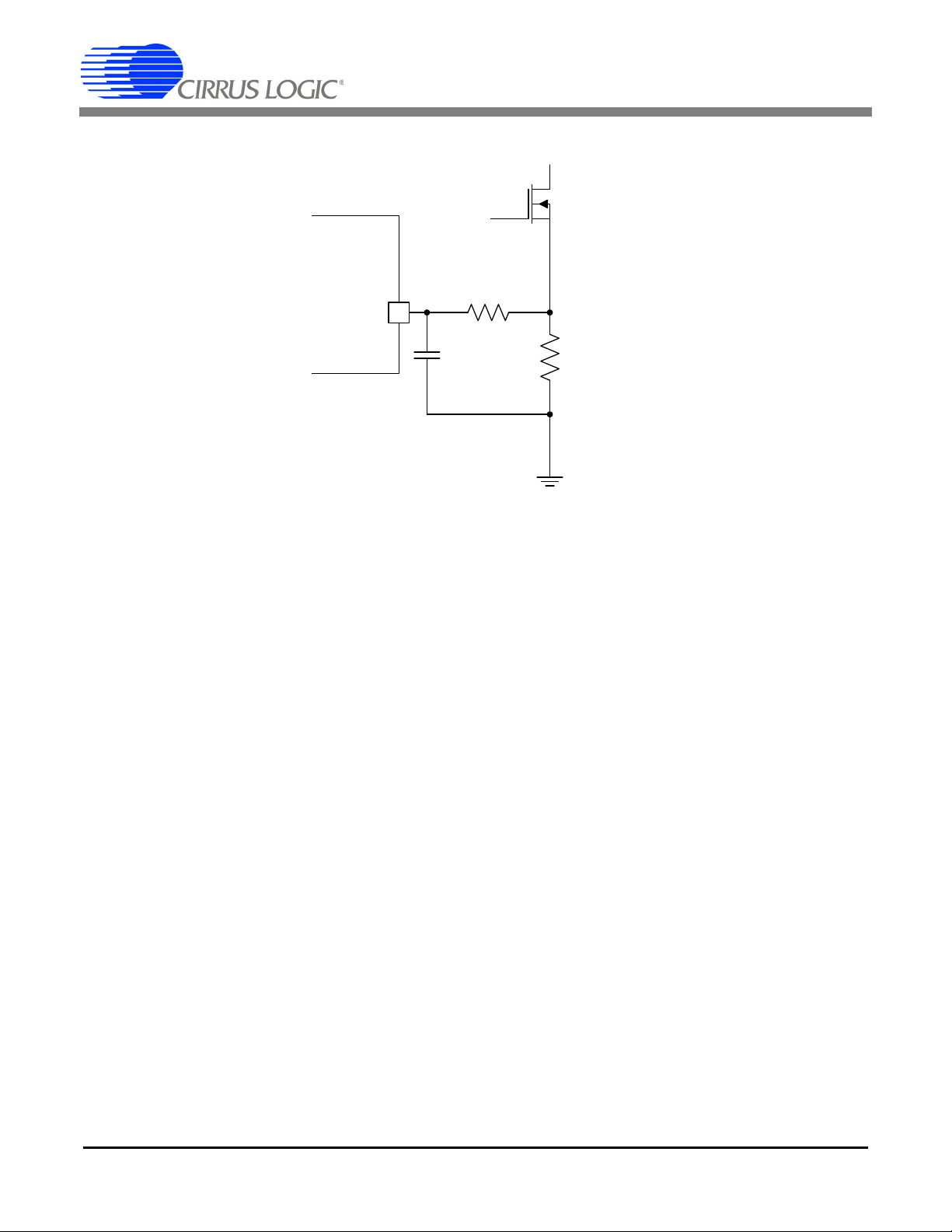
R
sense
R
cs
C
cs
CS1601
4
CS
Figure 1. Current Sense Filter
It is a general recommendation that a resistor (RCS) is used in series between the CS pin & the sense resistor (R
constant (TCS) of this should not be greater than 10 ns. This number indicates the delay the PCB circuitry adds and would linearly
add to the inherent delay in turning the gate off upon an overcurrent event.
The maximum capacitance that can be used is 1 nF, assuming R
tance is:
C
CS=TCS
Setting RCS to be 100, the equation yields:
= 100pF.
C
CS
Therefore, the recommended capacitance for the current-sense filter is 100 pF.
= 0.1. The equation for the current-sense filter capaci-
Sense
R
CS
Sense
). The time
2
Page 3

AN353
This page intentionally blank.
3
Page 4

AN353
Contacting Cirrus Logic Support
For all product questions and inquiries contact a Cirrus Logic Sales Representative.
To find one nearest you go to http://www.cirrus.com
IMPORTANT NOTICE
Cirrus Logic, Inc. and its subsidiaries ("Cirrus") believe that the information contained in this document is accurate and reliable. However, the information is subject
to change without notice and is provided "AS IS" without warranty of any kind (express or implied). Customers are advised to obtain the latest version of relevant
information to verify, before placing orders, that information being relied on is current and complete. All products are sold subject to the terms and conditions of sale
supplied at the time of order acknowledgment, including those pertaining to warranty, indemnification, and limitation of liability. No responsibility is assumed by Cirrus
for the use of this information, including use of this information as the basis for manufacture or sale of any items, or for infringement of patents or other rights of third
parties. This document is the property of Cirrus and by furnishing this information, Cirrus grants no license, express or implied under any patents, mask work rights,
copyrights, trademarks, trade secrets or other intellectual property rights. Cirrus owns the copyrights associated with the information contained herein and gives consent for copies to be made of the information only for use within your organization with respect to Cirrus integrated circuits or other products of Cirrus. This consent
does not extend to other copying such as copying for general distribution, advertising or promotional purposes, or for creating any work for resale.
CERTAIN APPLICATIONS USING SEMICONDUCTOR PRODUCTS MAY INVOLVE POTENTIAL RISKS OF DEATH, PERSONAL INJURY, OR SEVERE PROPERTY OR ENVIRONMENTAL DAMAGE ("CRITICAL APPLICATIONS"). CIRRUS PRODUCTS ARE NOT DESIGNED, AUTHORIZED OR WARRANTED FOR USE
IN PRODUCTS SURGICALLY IMPLANTED INTO THE BODY, AUTOMOTIVE SAFETY OR SECURITY DEVICES, LIFE SUPPORT PRODUCTS OR OTHER CRITICAL APPLICATIONS. INCLUSION OF CIRRUS PRODUCTS IN SUCH APPLICATIONS IS UNDERSTOOD TO BE FULLY AT THE CUSTOMER'S RISK AND
CIRRUS DISCLAIMS AND MAKES NO WARRANTY, EXPRESS, STATUTORY OR IMPLIED, INCLUDING THE IMPLIED WARRANTIES OF MERCHANTABILITY
AND FITNESS FOR PARTICULAR PURPOSE, WITH REGARD TO ANY CIRRUS PRODUCT THAT IS USED IN SUCH A MANNER. IF THE CUSTOMER OR
CUSTOMER'S CUSTOMER USES OR PERMITS THE USE OF CIRRUS PRODUCTS IN CRITICAL APPLICATIONS, CUSTOMER AGREES, BY SUCH USE, TO
FULLY INDEMNIFY CIRRUS, ITS OFFICERS, DIRECTORS, EMPLOYEES, DISTRIBUTORS AND OTHER AGENTS FROM ANY AND ALL LIABILITY, INCLUDING ATTORNEYS' FEES AND COSTS, THAT MAY RESULT FROM OR ARISE IN CONNECTION WITH THESE USES.
Cirrus Logic, Cirrus, and the Cirrus Logic logo designs are trademarks of Cirrus Logic, Inc. All other brand and product names in this document may be trademarks
or service marks of their respective owners.
4
 Loading...