

Page 1
CS1501
CS1601
8
VDD
V
DD
7
GD
6
GND
GD OUT
GD
GND
CS
VDD
Buffer
S
1
R
1
R
2
R
3
TP
C
L
1nF
+15V
-15V
S
2
V
DD
AN352
Application Note
DRIVING MOSFETs WITH THE CS1501 & CS1601
1. Introduction
The CS1501 & CS1601 are high-performance digital power factor correction (PFC) controllers designed for switching mode power supply (SMPS) & lighting applications. This papers discusses the basics of driving power MOSFETs, including so me guidelines for layout & component choices.
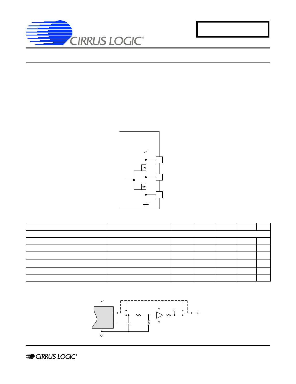
2. CS1501 & CS1601 Gate Drive
The CS1501 & CS1601 internal gate driver is a dual MOSFET between VDD & GND.
The CS1501 & CS1601 parameters for its internal gate drive are listed below.
Parameter Condition Symbol Min Typ Max Unit
PFC Gate Drive
Output Source Resistance IGD= 100 mA, VDD=13V R
Output Sink Resistance IGD=-200mA,VDD=13V R
Rise Time
Fall Time
1
1
CL=1nF,VDD=13V t
CL=1nF,VDD=13V t
OH
OL
r
f
-9-Ω
-6-Ω
-3245ns
-1525ns
Output Voltage Low State IGD=-200mA,VDD=13V Vol - 0.9 1.3 V
Output Voltage High State IGD= 100 mA, VDD=13V Voh 11.3 11.8 - V
is defined as the capacitive load that the IC drives. For test purposes, load capacitance (CL) is 1 nF and is
1. C
L
connected as shown in the following diagram.
http://www.cirrus.com
Copyright Cirrus Logic, Inc. 2011
(All Rights Reserved)
AN352REV1
MAR ‘11
Page 2
AN352
A
7
R
g
7
GD
C
7
R
g
7
GD
B
7
R
g
7
GD
7
4
CS
7
4
CS
7
4
CS
R
cs
R
cs
R
cs
Q
off
D
off
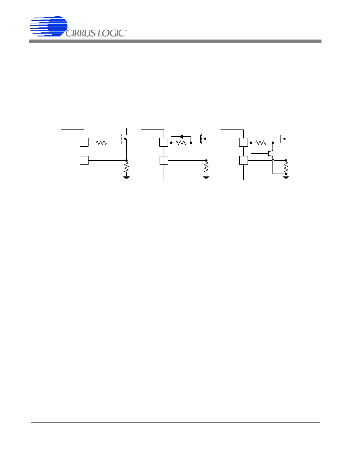
3. Gate Drive External Components
High voltage MOSFETs generally have low gate-charge capacitance. As a result, they can be driven di rectly from the IC. The
CS1501 & CS1601 are designed to function as power factor corre cted SMPS working in discontinu ous mode (DCM). They are
best suited for supplies less than150 W. With relatively low switching frequencies (<70kH z) and l ow switching current, the b enefits of having very fast rise & fall times is reduced.
- The simplest implementation is a low-value resistor (~10 Ω) in series with the driver & MOSFET gate. (Option A.)
- Efficiency can be improved by adding a diode in parallel with the resistor. (Option B.) This turns the MOSFET off quickly,
and reduces the I – V losses as the voltage rises while current is still flowing.
- Adding a small-signal PNP transistor further reduces turn off time. (Option C.)
4. PCB Layout
The IC should be placed as close as possible to the MOSFET, with a short, direct connectio n from the driver to the gate . The
return path from the FET source to the IC should also be minimal. This reduces issues with PCB trace impedance interfering with
the drive — both resistive and inductive. For further details, please refer to Cirrus Logic application note AN350, CS1601 Layout
Guidelines.
5. Summary
Simple gate drive structures are sufficient for most PFC applications. A choice from one of the sch emes listed above wi ll work,
with focus on following basic layout rules.
2 AN352REV1
Page 3

AN352
This page intentionally blank.
AN352REV1 3
Page 4

6. Revision History
Contacting Cirrus Logic Support
For all product questions and inquiries contact a Cirrus Logic Sales Representative.
To find one nearest you go to http://www.cirrus.com
IMPORTANT NOTICE
Cirrus Logic, Inc. and its subsidi a ries ("Cirrus") believe that the information contained in this document is accurate and reliable. However, the information is subject
to change without notice and is provided "AS IS" without warranty of any kind (express or implied). Customers are advised to obtain the latest version of relevant
information to verify, before placing orders, that information being relied on is current and complete. All products are sold subject to the terms and conditions of sale
supplied at the time of order acknowle dgment, including tho se pertaining to warra nty, indemnification, and l imitation of liability. No responsibility is assumed by Cirrus
for the use of this information, including use of this inform ation a s the basis for m anufactur e or sale of an y items, or for infringement of patents or other rights of third
parties. This document is the property of Cirrus and by furnishing this information, Cirrus grants no license, express or implied under any patents, mask work rights,
copyrights, trademarks, trade secrets or other intellectual pro perty rights. Cirrus owns the copyr ights associated with the information con tained herein a nd gives consent for copies to be made of the information only for use within your organiza tion with resp ect to Cirrus inte grated circu its or other products of Cirrus. This consent
does not extend to other copying such as copying for general distribution, advertising or promotional purposes, or for creating any work for resale.
CERTAIN APPLICATIONS USING SEMICONDUCTOR PRODUCTS MAY INVOLVE POTENTIAL RISKS OF DEATH, PERSONAL INJURY, OR SEVERE PROPERTY OR ENVIRONMENTAL DAMAGE ("CRITICAL APPLICATIONS"). CIRRUS PRODUCTS ARE NOT DESIGNED, AUTHORIZED OR WARRANTED FOR USE
IN PRODUCTS SURGICALLY IMPLANTED INTO THE BODY, AUTOMOTIVE SAFETY OR SECU RITY DEVICES, LIFE SUPPOR T PRODUCTS OR OTHE R CRITICAL APPLICATIONS. INCLUSION OF CIRRUS PRODUCTS IN SUCH APPLICATIONS IS UNDERSTOOD TO BE FULLY AT THE CUSTOMER'S RISK AND
CIRRUS DISCLAIMS AND MAKES NO WARRANTY, EXPRESS, STATUTORY OR IMPLIED, INCLUDING THE IMPLIED WARRANTIES OF MERCHANTABILITY
AND FITNESS FOR PARTICULAR PURPOSE, WITH REGARD TO ANY CIRRUS PRODUCT THAT IS USED IN SUCH A MANNER. IF THE CUSTOMER OR
CUSTOMER'S CUSTOMER USES OR PERMITS THE USE OF CIRRUS PRODUCTS IN CRITICAL APPLICATIONS, CUSTOMER AGREES, BY SUCH USE, TO
FULLY INDEMNIFY CIRRUS, ITS OFFICERS, DIRECTORS, EMPLOYEES, DISTRIBUTORS AND OTHER AGENTS FROM ANY AND AL L LI AB ILI T Y, I NCLUDING ATTORNEYS' FEES AND COSTS, THAT MAY RESULT FROM OR ARISE IN CONNECTION WITH THESE USES.
Cirrus Logic, Cirrus, and the Cirrus Logic logo de signs ar e trade mar ks of Cirrus Logic, Inc. All other br and a nd pro du ct nam es in this docu me nt may be tradem arks
or service marks of their respective owners.
Revision Date Changes
REV1 MAR 2011 Initial Release.
AN352
4 AN352REV1
 Loading...