

Page 1
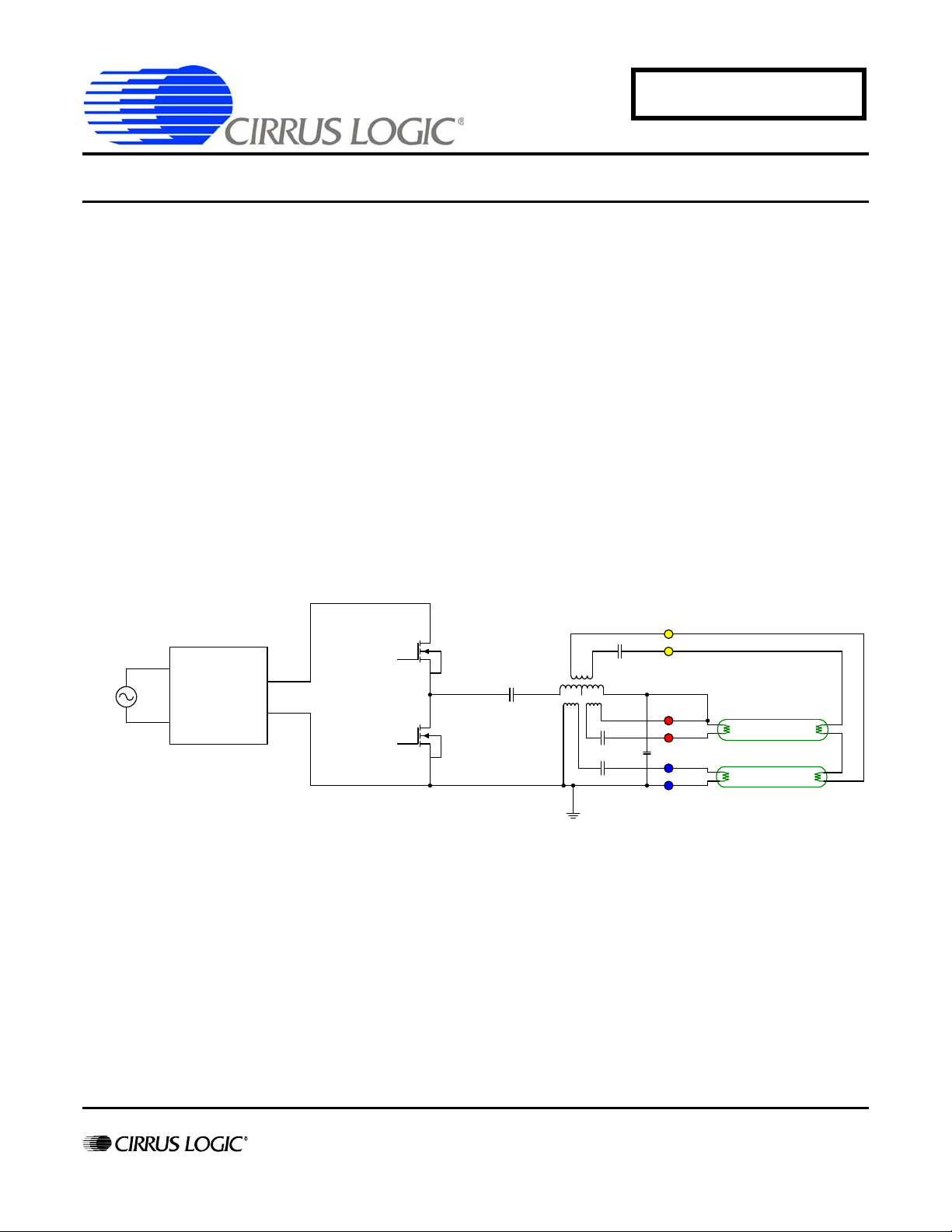
Lamp
Lamp
Bridge + EMI Filter +
Boost PFC
AC
Input
Figure 1. Example Ballast Second Stage and Lamp Connections
AN349
Application Note
MIGRATING FROM THE L6562 TO THE
CS1601 POWER FACTOR CORRECTION IC
1. Introduction
The CS1601 belongs to Cirrus Logic's family of industry-first digital Power Factor Correction (PFC) ICs offering best-in-class performance. The CS1601 has been optimized for lighting applications. This document compares the CS16 01 with the ST Microelectronics L6562. A commercially available ballast designed to light two T05HO lamp s is used as a benchmark. The test
conditions and setup for the ballast are described in Section 2. The third section of the document details the advantages of using
the CS1601 over the L6562. The fourth section discusses the differences in theory of operation. Section 5 compares the feature
sets of L6562 and CS1601. Section 6 describes a step -by-step pro cedure to show how to migrate an L6562-ba sed PFC frontend pre-regulator to a CS1601-based solution.
2. Description of Test Setup
Fluorescent ballasts are a challenging application for PFC due to the presence of large load tra nsients and strict THD requirements in a highly cost-sensitive market. Given the wide input voltage ra nge of the application and the demanding form factor
requirements for these applications, many design trade-offs have to be made to complete a design using the current analog Critical Conduction Mode (CRM) solutions.
2.1 Ballast Specifications & Requirements
- Input Voltage Range: 108V to 305V 50/60Hz
- Output Load: 2x T5HO lamps amounting to ~108W nominal
- Link capacitor: 2x 47F, 250V caps in series
- Low THD (<10%)
- High Power Factor (>0.9)
- No lamp flicker under any test condition
Copyright Cirrus Logic, Inc. 2011
http://www.cirrus.com
(All Rights Reserved)
MAR ‘11
AN349REV1
Page 2
AN349
THD Vs Line @ 60Hz
0
2
4
6
8
10
12
14
16
80 100 120 140 160 180 200 220 240 260 280 300
Line Voltage (V)
D
CS1601
ST L6562
3. Advantages of CS1601 over L6562
The CS1601 uses a revolutionary digital algorithm that has significant advantages ov er the existing anal og CRM-based L6 562.
The major advantages are described in the following sections.
3.1 Smaller Boost Inductor
The CS1601 has a digitally implemented variable-frequency, discontinu ous conduction mode (VF-DCM) -based algori thm that
permits delivering the same power and the same peak current rati ngs with a significa ntly smaller inductance . This results in an
inductor which is considerably smaller in physical dimensions. In the fluorescent ballast appl ication introduce d in Section 2, migration from a L6562-based solution to one using the CS1601 re sulted in the inductor being 45% smaller. The same inductor
could be wound with 26% fewer turns or in a smaller core size which would result in a more compact design. The 2x EE19 core
sets used in some L6562-based fluorescent ballasts could be replaced with a single EE25 inductor reducing the total cost and
size of the final solution.
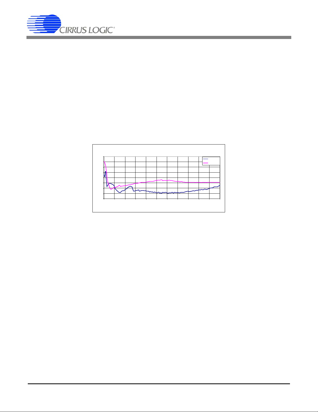
3.2 Lower Total Harmonic Distortion (THD)
The CS1601-based design has lower THD than the L6562-based solution. In the fluorescent ballast example, it can be seen that
the THD across the line at full load was more than 2.5% lower than L6562 as shown in Figure 2.
% TH
Figure 2. Comparison of THD vs. AC Line Voltage
The L6562 cannot support large differential filter capacitors on the DC side of the brid ge rectifier. In CRM controllers, the maximum switching frequency at the trough of the AC line is theoretically infinity. The L6562 sets a limit on this maximum, increasing
distortion of the AC line when a larger capacitor is placed across the rectified (DC) AC line. The L6562-based ballast necessitates
expensive AC capacitors placed on the AC line side of the bridge rectifier, increasing the cost of the EMI filter. Since the THD in
the CS1601-based solution is significantly lower, it allows the designer to reduce the EMI filter cost by moving a substantial portion of the differential filter capacitance to the DC side of the bridge rectifier. This eliminates the need for expensive AC capacitors
and reduces overall bill of material (BOM) cost.
3.3 Light Load Performance
The flexibility of moving filters to either side of the rectifier also offers another significant advantage over the L6562 with respect
to light-load PF and high-line-voltage THD. In traditional analog solutions, placing capacitors at the output of the bridge rectifiers
increases THD, especially at light-load conditions and high line voltage. At the trough of the AC line, CRM controllers run at very
high frequencies and switch intermittently to limit switching losses. Placing capacitors at the input side of the bridge reduces PF
since the EMI capacitor swings to twice the input voltage. Power supply design ers have to make trade-offs between light load
efficiency, power factor, and THD. The L6562 has errors and delays resulting from the multiplier, comparator, and gate drivers.
These result in errors in peak current at light loads. In the trough these cause significant deterioration of THD performance. As a
workaround to this problem, traditional CRM controllers have to greatly increase the inductance of the boost inductor to limit the
slope of the current and limit the error in peak current that is caused. Since the CS1601 is a variable-frequency DC M control le r
with different frequency profile, the limitations encountered when using the L6562 are not present in a system designed with the
CS1601. The CS1601 offers optimal performance with minimal design constraints.
3.4 Near Unity Power Factor
Improved THD performance necessitates large AC capacitors for differential mode EMI filters. Because the voltage swing on capacitors on the AC line side of the bridge rectifier is twice that of the capacitors placed on the DC side of the bridge, power factor
is reduced. Figure 3 compares the PF between the L6562-based ballast and the CS1601-based ballast. The CS1601 maintains
2 AN349REV1
Page 3
AN349
PF Vs Line @ 60Hz
0.93
0.94
0.95
0.96
0.97
0.98
0.99
1
1.01
80 100 120 140 160 180 200 220 240 260 280 300
Inpu t Voltage (V)
PF
CS1601
ST L6562
near unity power factor across the operating input voltage range. The CS1601-based solutions grea tly minimizes the need for
making this trade-off. The CS1601 can provide very low distortion at near unity PF.
Figure 3. Comparison of Power Factor vs. AC Line Voltage
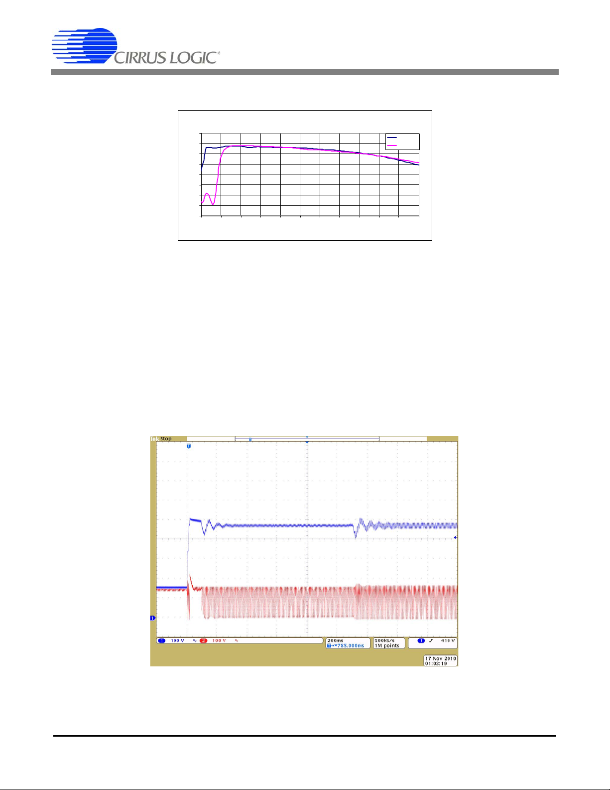
3.5 Lower Link Overshoot During Lamp Strike
The CS1601-based ballast demonstrates better performance during lamp strike and start-up. The scope capture of the lamp
strike with the L6562 is shown in Figure 4. The scope capture of the lamp strike with the CS1601 is shown in Figure 5. In both
the scope captures, the PFC output is presented in blue and the bridge rectifier output signal is presented in red. From Figure 4,
it can be observed that with the L6562-based ballast, during lamp start-up, the link voltage rails up to 520V before settling down
to the nominal value of 485V. In the CS1601-based ballast, the link voltage does not go above 492V, which is the voltage threshold for the over voltage protection (OVP). Since the output capacitors are rated for 500V (Two 47uF, 250V capacitors in series),
the lifetime of these capacitors are improved by keeping the voltage below 500V under all conditions. The CS1601 requires a
lower inductance for the same power level, resulting in less stored energy during startup. At the end of startup, the stored energy
is transferred to the output bulk capacitor. Less stored energy results in a smaller V
Note: Neither solution produced any flicker during lamp strike.
overshoot.
link
AN349REV1 3
Figure 4. Ballast Startup with L6562
Page 4
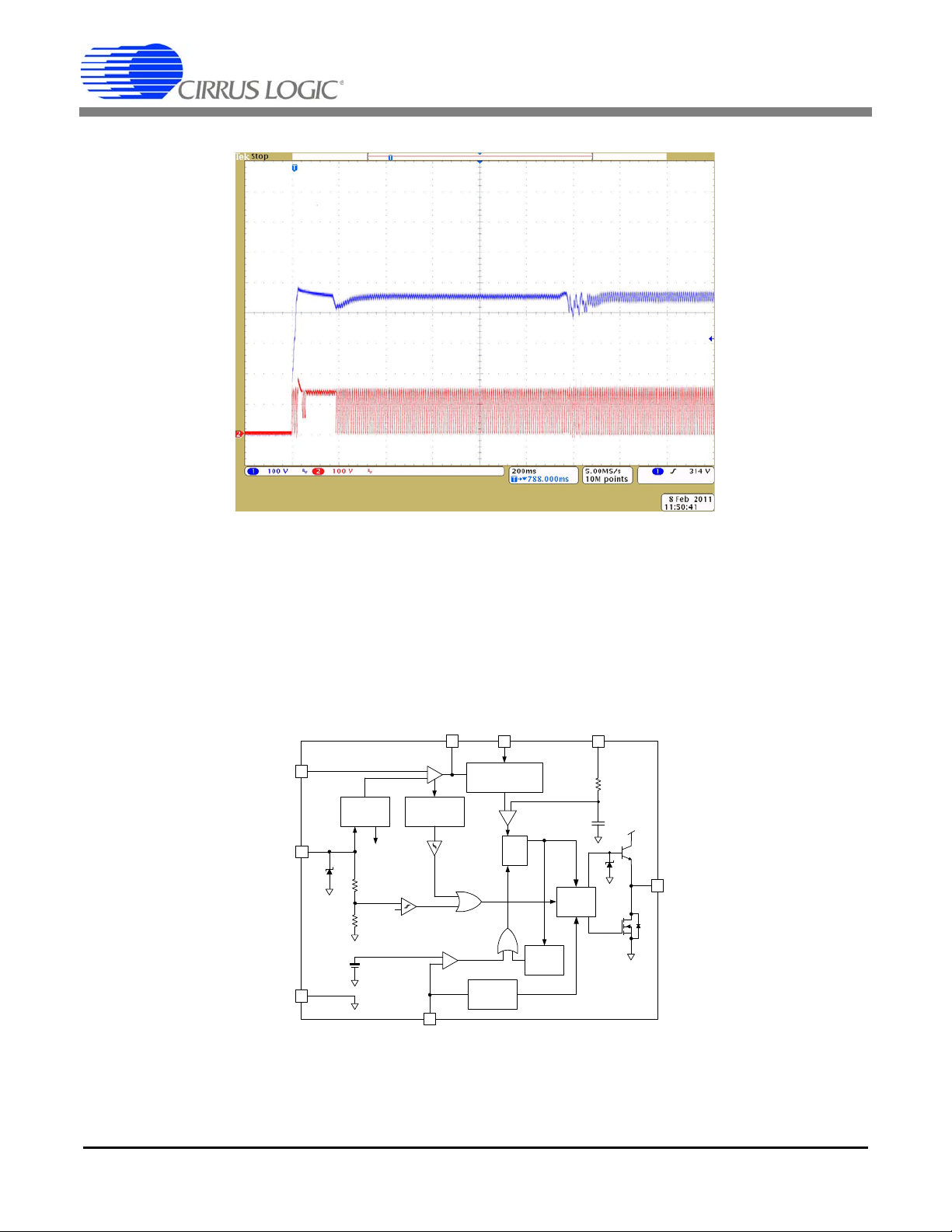
Figure 5. Ballast Startup with CS1601
4
CS
7
GD
2
COMP
VCC
GND
V
CC
8
V
Ref2
Starter
Stop
R1
+
-
+
-
Voltage
Regulator
Overvoltage
Detection
R2
40k
Multiplier & THD
Optimizer
Disable
Driver
25V
+
-
RSQ
+
-
5
ZCD
INV
1
UVLO
6
Starter
2.1V
1.6V
Zero Current
Detector
15V
5pF
MULT
3
Internal
Supply 7V
2.5V
AN349
4. Theory of Operation
Figure 4 and Figure 5 are the internal block diagrams of the L6562 and the CS1601, respectively.
4 AN349REV1
Figure 6. L6562 Block Diagram
Page 5
AN349
V
Z
POR +
-
V
ST(th)
V
STP(th)
Voltage
Regulator
8
VDD
5
ZCD
+
-
V
ZCD(th)
7
GD
Zero Cross
Detect
6
GND
IFB
IAC
V
DD
t
LEB
V
DD
15k
24k
3
V
DD
15k
24k
1
ADC
ADC
t
ZCB
4
CS
600
+
-
CS
Threshold
+
-
CS Clamp
V
CS(clamp )
V
CS(t h)
STBY
V
DD
600k
2
Swit ching Fre q uency of L6562 Acr o ss Lin e
0
10
20
30
40
50
60
70
80
0 45 90 135 180 225 270 315 360
Pha s e Angl e (degrees)
Swi tching Frequency (KHz)
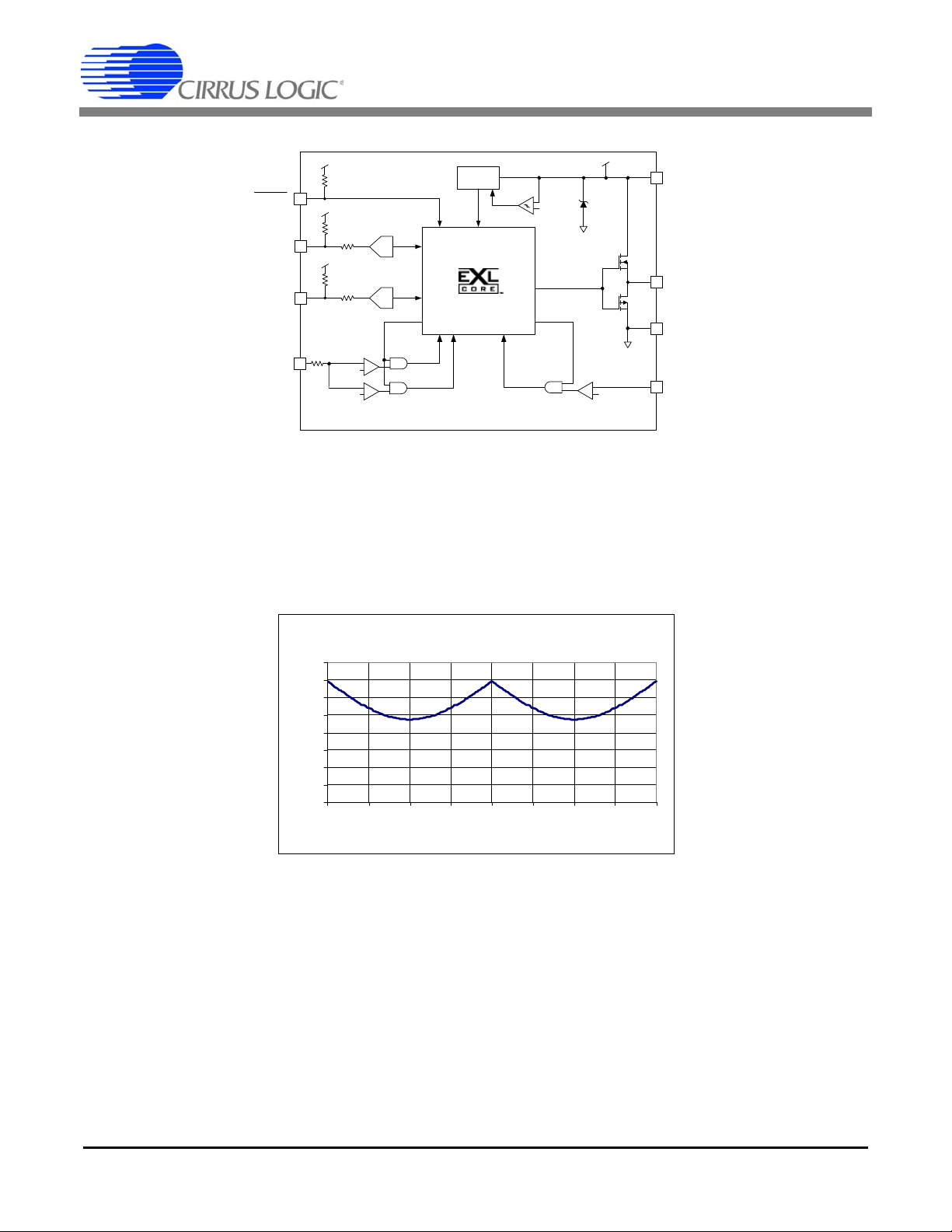
Figure 7. CS1601 Block Diagram
The basic principle of operation of the L6562 can be summarized as follows:
- The L6562 is a CRM controller which sets a peak current reference which is a function of the line voltage multiplied with
the output of the error amplifier.
- During the design phase, the maximum steady-state power is defined by the current-sense resistor setting the
overcurrent threshold. The selection of inductor shifts the frequency profile across load conditions and line voltages.
- The zero-cross detect (ZCD) pin detects when the inductor current resets to zero.
The frequency of operation across the line voltage is shown in Figure 8.
Figure 8. L6562 Switching Frequency vs. Line Voltage at Low Line
The basic principle of operation of CS1601 can be summarized as follows :
- The CS1601 is a mixed DCM/CRM controller and is a voltage-mode IC which measures the output voltage and computes
AN349REV1 5
a given switching frequency scheme at every line voltage.
- The maximum power is specified by the selection of the inductor. The frequency is computed based on the line voltage.
- The CS1601 measures the line (V
- The EXL Core™ signal processing core computes the correct T
and link voltages and programmed PID coefficients.
- The EXL Core turns off th e ga te once T
- The EXL Core counts until T
- Figure 9 and Figure 10 show the frequency profile across the operating range for a CS1601-based solution.
time is reached or until zero-cross detection (ZCD) — whichever is first.
off
) and link (V
rect
is reached.
on
) voltages and compares them against a reference.
link
, T
, and switching frequency for the measured line
on
off
Page 6

Figure 9 shows the frequency profile across the line voltage for CS1601-based solution.
0
10
20
30
40
50
60
70
80
0 45 90 135 180 225 270 315 360
Phase Angle (degrees)
Switching Frequency (Khz)
DCM
DCM DCM
CRM
DCM
DCM DCM
CRM
Max Fr equency (KHz )
Line Vol tage (V)
56
40
70
46
90 147 265
Po > 40%
Po < 20%
181 230
Figure 9. CS1601 Switching Frequency vs. Line Voltage at Low Line
Figure 10 shows the frequency of operation of the system across load and line condition.
AN349
Figure 10. Frequency of Operation Across Line and Load Condition
6 AN349REV1
Page 7

AN349
L
Vin
min
2
V
link
2Vin
min
–
2FswVin
min
---------------------------------------------------------------------------------
=
4.1 Boost Inductor Size
Like the L6562-based designs, the size of the boost inductor when using the CS1601 is determined by th e amount of energy
pushed by the inductor at the minimum input voltage during full-load operation.
At the peak of the minimum input line voltage, and at full load, the operation of the CS1601 is identical to that of L6562. Therefore
as shown in Figure 9, the CS1601-based PFC system operates in CRM mode at the peak of the line. Peak currents for both the
systems are the same. Since the inductors in both the systems are pushing maximum power at the peak of the minimum line
voltage while maintaining CRM operation, the following equation for calculating the inductor size is:
Where,
L = boost inductor value
Vin
= minimum line voltage for which PFC is designed (RMS)
min
= PFC Output/Link Voltage
V
link
Fsw = frequency of PFC at the peak of the line voltage
Pin= input power to the PFC
Comparing Figure 8 and Figure 9, it can be seen that for the CS1601, Fsw corresponds to the maximum switching frequency
(nominally 70 kHz). For the L6562, Fsw co rresponds to the minimum switching frequency, which is usu ally around 40-45k Hz in
most designs. Assuming the same margin for overcurrent conditions, the CS1601 needs an inductance which is 45% smaller
than the corresponding L6562-based design.
AN349REV1 7
Page 8

5. Feature Set
Feature Set L6562 CS1601
Over Current Protection
99
Over Voltage Protection
99
Over Temperature Protection
99
Open /Short Circuit Protection
8
9
Brownout Protection
8 9
Vcc Under Voltage Lockout
99
Over Power Protection
8
9
Feature Set L6562 CS1601
ZCD
99
Current Sense
99
Power Saving Standby Mode
8 9
8pin SOIC package with Industry Standard Pin out
99
Adaptive Switching frequency control
8 9
Specifications L6562 CS1601
Current Consumption during normal operation (mA) 2.5 1.7
Gate Drive Source Ton time (ns) 80 45
Gate Drive Sink Current Capability (ns) 70 25
UVLO of Vcc (V) 10.3 8.4
OVP Hysteresis (%) 4% 1%
The following tables compare the major feature sets of CS1601 and L6562.
5.1 Protection Feature Set
5.2 Performance Feature Set
AN349
5.3 Other Specifications
8 AN349REV1
Page 9

AN349
CSPFC Curre nt Sense
IFBLink Voltage Sense
ZCD PFC Ze ro-current Det e ct
GND
Ground
GD PFC Gate D riv er
VDD I C Supply Volt age
STBYS tandby
IACRectifier V oltage Sense
4
3
2
1
5
6
7
8
CS1601
CSI nput to PWM Comparat or
INVI nvertin g Input of Error Ampl if i er
ZCD Demag. S ensing Input
GND
Ground
GD Gat e Driver Ouput
VCC I C Supply Voltage
COMPOutput of Error Ampl i fi er
MULTMain Input t o Multiplier
4
3
2
1
5
6
7
8
L6562
R1
1.5M
R2
1.5M
R5
68K
R7
0. 8 2
0. 6 W
R9
750K
R10
750K
8
1
D1
C1
0.47uF
400V
C7
100 uF
Regulated
DC Output
Q1
AC
Mains
BR1
BR1
BR1
BR1
L6562
GD
ZCD
INV
GND
CSMULT
VDD
L
B
6
3
5
7
4
V
DD
R11
9.53K
C4
2.2 uF
R6
12K
R3
22K
C2
100nF
2
C5
680 nF
C3
4.7uF
R8
0.82
0.6W
COMP
6. Migrating an Existing Design to Use the CS1601
6.1 Footprint Compatibility
The CS1601 is packaged in the industry-standard 8-pin SOIC and is footprint-compa tible with the L6562. Fig ure 11 shows the
Pin assignments of the CS1601 and the L6562. Figure 12 shows the typical PFC section on the ballast using the L6562. Figure
13 shows the typical PFC section of the ballast using the CS1601. In both schematics, the V
It will be discussed in a separate section.
Although the CS1601 is footprint compatible with the L6562, it is not a direct drop-in-replacement. Changes to the L6562 system
BOM are necessary as shown in Figure 13.
generation is not demonstrated.
cc
Figure 11. Pin Assignments for CS1601 and L6562
6.2 BOM Changes Necessary to use CS1601
The following is a typical connection diagram for a ballast using the L6562.
Figure 12. PFC Schematic Of Benchmark Ballast Using L6562
AN349REV1 9
Page 10

AN349
CHANGECHANGE
ADD
DELETEDELETE
DELETE
CHANGE
ADD
R1
1.72M
R2
1.72M
R5
68k
R7
0. 8 2
0.6W
R10
1.72M
R11
1.72M
8
1
D1
C1
.47 u F
400V
C7
100uF
Regulated
DC Output
Q1
AC
Mains
BR1
BR1
BR1
BR1
CS1601
GD
ZCD
IFB
GND
CSIAC
VDD
L
B
6
3
5
7
4
V
DD
R9
9.53k
C4
2.2 uF
R6
12k
R3
22k
C2
100pF
2
C5
680 nF
R4
1.75k
C3
4.7uF
R8
0.82
0.6W
C6
100pF
25V
STBY
C8
33 pF
IC Inductance (uH) Peak Current (A) Turns Ratio (Np:Ns) Frequency (KHz)
L6562 700 4.5 10 45
CS1601 380 4.5 10 70
IC
Min Vcc @
Turn ON (V)
Max Vcc @
Turn OFF (V)
Nominal Vcc (V)
L6562 13 10 11 -22
CS1601 10.8 8.5 9 -17
Make changes to the schematic as shown. Note that capacitor C6 can be between pi n 1 and GND or pin 1 a nd VDD, b ased on
routing considerations. Also, capacitor C2 can be between pin 3 and GND or pin 3 and VDD. Refer to application note AN3 46 -
CS1501 & CS1601 PCB Layout Guidelines for further information.
It is recommended to place a 33pF capacitor (C8) between pin 5 and GND. It is important that the capacitor be at close to the
pins as possible. Also, the ground side of the capacitor should be placed away from the gate drive ground return path.
Figure 13. PFC Schematic Of Benchmark Ballast Using CS1601
6.3 Boost Inductor Design
The difference in the boost inductor can be understood from Figure 8 and Figure 9. F or the fluorescen t ballast under study, the
inductor difference is shown in table below.
Table 1. Boost Inductor Comparison
6.4 PCB Layout Changes
The signal ground of the ballast should be re-routed to refer ence the negative of the current-sense resistor. Depending on the
distance, another place where the ground can be referenced is the negative of the electrolytic bulk capacitor. Resistor R3 is referenced to be close to the 100 nF capacitor. Refer to app lication note AN346 - CS1501 & CS1601 PCB Layout Guidelines for
detailed information on best layout practices when designing systems based upon the CS1601.
6.5 Auxiliary Supply Design
There are many ways to design the auxiliary supply. However, the table below shows some differences be tween L6562 and
CS1601 with respect to aux supply design.
Table 2. VCC Generation
10 AN349REV1
Page 11

AN349
R1
R2
R3
D1
Z1 Aux
C1
V
rect
In almost all fluorescent ballast applications, there are no requirements for light-load efficiency. The most common topology used
for supplying Vcc is shown in Figure 14. When migrating to the CS1601, no changes are necessary except that diode Z1 should
be a 13V to 15V zener diode. Capacitor C1 is the Vcc capacitor and should be a 4.7F, 25V ceramic capacitor. At the generation
of the aux supply, there can be a larger storage capacitor as well.
Figure 14. Typical Inexpensive Aux Supply
It is important to note that there are no changes needed in the second stage to make it compatible with the CS1601. However, if
the second stage is used to provide auxiliary supply to the entire ballast, care must be taken to meet the specifications of the
CS1601 as described in Table 2.
AN349REV1 11
Page 12

AN349
L6562
3
MULT
Rac2
R
ac
1
C
ac
V
rect
CS1601
3
IAC
R
st
Rac2
R
ac
1
C
ac
V
rect
6.6 Noise Issues When Using CS1601 to replace L6562
For an existing design using the L6562, attempting to use the CS1601 with the component values of the L6562 design may lead
to instability and unpredictable performance and system behavior. Design parameters that should be modified for the CS1601
pins IAC & IFB are described in the following two sections.
For details on the ST Microelectronics L6562, refer to ST Microelectronics application note AN1895.
6.6.1 IAC – PIN 3
Based on the AN1895, recommended components used on the MULT pin on L6562 (pin 3) have the following characteristics:
1, Rac2 = 620k (Rac=1.24M)
- R
ac
- Rst = 10k (Not required for CS1601.)
- C
= 10nF
ac
- The filter pole for this node is at Fp = 1 (2R
- The filtering cap, Cac, is chosen to match the pole at 1.6kHz.
- C
.
= ~8nF. Using a standard value, Cac is 8.2nF or 10nF.
ac
Cac Gain) = 1.6kHz (approx.)
ac
Figure 15. Input Voltage (AC) Sense Noise Decoupling
When using the CS1601, recommended components used on the IAC pin (pin 3) have the following characteristics:
1, Rac2 = 875k (Rac=1.75M)
- R
ac
- R
= Not required.
NOTE: For CS1601, Fp should be higher than 1.2kHz. A lower value can deteriorate the power factor of the system.
st
- C
= 10nF
ac
- The filter pole for this node is at Fp = 1 (2R
- The bandwidth on the IAC pin of CS1601 should be limited to approximately 1.6kHz.
- The internal impedance on pin IAC (R
- The filtering cap, C
- C
= ~8nF. Using a standard value, Cac is 8.2nF or 10nF.
ac
, is chosen to match the pole at 1.6kHz.
ac
)=~12k.
int
Cac Gain) = 1.6kHz (approx.)
ac
12 AN349REV1
Page 13

AN349
Cfb1
L6562
INV
Rfb2
R
fb
1
C
fb
2
V
link
Rfb3
COMP
1
2
V
ref
Rfb4
CS1601
IFB
Rfb2
R
fb
1
C
fb
V
link
1
2
V
DD
600 k
ADC
STBY
6.6.2 IFB - Pin 1
The filter pole (corner) on pin 1 is calculated by:
Fp = 1 (2Rfb Cfb2 Gain)
From the L6562 data sheet, we will set the gain of the op-amp to 60 dB at DC, which results in a very low corner frequency. The
CS1601 does not require this low corner frequency created by the feedback components. The following changes should be made
when using the CS1601:
- Cfb1, Cfb2, Rfb3, and Rfb4 are removed.
- R
1 and Rfb2 are changed to the appropriate value to get the required link voltage (1.75M for V
fb
- C
is added to provide noise filtering on the IFB pin.
fb
The internal impedance of the IFB pin is the same as pin IAC (~12k), so it is recommended that the capacitor value be the same
as used on pin IAC.
=460V)
link
Figure 16. Output Voltage (DC) Sense Noise De-coupling
7. Conclusion
It has been shown that there are significant bene fits from selecting th e CS1 601 over the L6562. T he advantages w ere demonstrated in an equivalent comparison by retrofitting an existing ballast product designed with the L6562 with the CS1601.
When using the CS1601, care should be taken to adequately protect the device from noise through the use of decoupling capacitors & careful layout. The value of the capacitors should be also considered.
AN349REV1 13
Page 14

8. Revision History
Contacting Cirrus Logic Support
For all product questions and inquiries contact a Cirrus Logic Sales Representative.
To find one nearest you go to http://www.cirrus.com
IMPORTANT NOTICE
Cirrus Logic, Inc. and its subsidiaries ("Cirrus") believe that the information contained in this document is accurate and reliable. However, the information is subject
to change without notice and is provided "AS IS" without warranty of any kind (express or implied). Customers are advised to obtain the latest version of relevant
information to verify, before placing orders, that information being relied on is current and complete. All products are sold subject to the terms and conditions of sale
supplied at the time of order acknowle dgment, including tho se pertaining to warra nty, indemnification, and l imitation of liability. No responsibility is assumed by Cirrus
for the use of this information, including use of this inform ation a s the basis for m anufactur e or sale of an y items, or for infringement of patents or other rights of third
parties. This document is the property of Cirrus and by furnishing this information, Cirrus grants no license, express or implied under any patents, mask work rights,
copyrights, trademarks, trade secrets or other intellectual pro perty rights. Cirrus owns the copyr ights associated with the information con tained herein a nd gives consent for copies to be made of the information only for use within your organiza tion with resp ect to Cirrus inte grated circu its or other products of Cirrus. This consent
does not extend to other copying such as copying for general distribution, advertising or promotional purposes, or for creating any work for resale.
CERTAIN APPLICATIONS USING SEMICONDUCTOR PRODUCTS MAY INVOLVE POTENTIAL RISKS OF DEATH, PERSONAL INJURY, OR SEVERE PROPERTY OR ENVIRONMENTAL DAMAGE ("CRITICAL APPLICATIONS"). CIRRUS PRODUCTS ARE NOT DESIGNED, AUTHORIZED OR WARRANTED FOR USE
IN PRODUCTS SURGICALLY IMPLANTED INTO THE BODY, AUTOMOTIVE SAFETY OR SECU RITY DEVICES, LIFE SUPPOR T PRODUCTS OR OTHE R CRITICAL APPLICATIONS. INCLUSION OF CIRRUS PRODUCTS IN SUCH APPLICATIONS IS UNDERSTOOD TO BE FULLY AT THE CUSTOMER'S RISK AND
CIRRUS DISCLAIMS AND MAKES NO WARRANTY, EXPRESS, STATUTORY OR IMPLIED, INCLUDING THE IMPLIED WARRANTIES OF MERCHANTABILITY
AND FITNESS FOR PARTICULAR PURPOSE, WITH REGARD TO ANY CIRRUS PRODUCT THAT IS USED IN SUCH A MANNER. IF THE CUSTOMER OR
CUSTOMER'S CUSTOMER USES OR PERMITS THE USE OF CIRRUS PRODUCTS IN CRITICAL APPLICATIONS, CUSTOMER AGREES, BY SUCH USE, TO
FULLY INDEMNIFY CIRRUS, ITS OFFICERS, DIRECTORS, EMPLOYEES, DISTRIBUTORS AND OTHER AGENTS FROM ANY AND AL L LI AB ILI T Y, I NCLUDING ATTORNEYS' FEES AND COSTS, THAT MAY RESULT FROM OR ARISE IN CONNECTION WITH THESE USES.
Cirrus Logic, Cirrus, and the Cirrus Logic logo de signs ar e trade mar ks of Cirrus Logic, Inc. All other br and a nd pro du ct nam es in this docu me nt may be tradem arks
or service marks of their respective owners.
Revision Date Changes
REV1 MAR 2011 Initial Release.
AN349
14 AN349REV1
 Loading...