

Page 1
AN339
-110
-90
-108
-106
-104
-102
-100
-98
-96
-94
-92
d
B
r
A
20 20k50 100 200 500 1k 2k 5k 10k
Hz
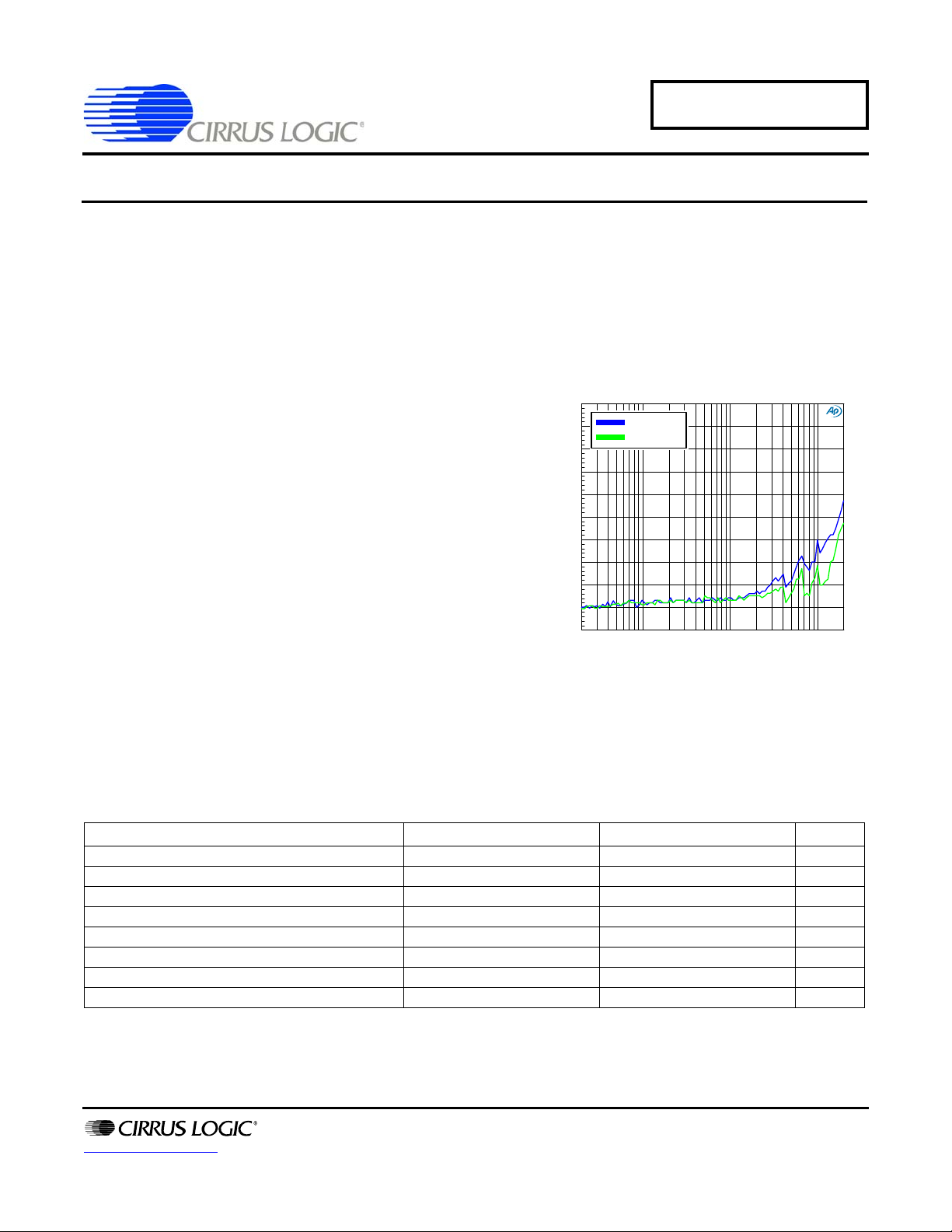
Figure 1. DAC THD+N
CS8414
CS8416
CS8416 Delivers Performance Gains Over CS8413/14
by
Jonathan Schwartz
1. INTRODUCTION
The CS8413/14 S/PDIF receivers have long held a position of respect as the industry-favored receivers for recovered clock quality. As of early 2009, an upcoming end-of-life of these products has many system designers wondering what their next move will be, and where they’ll go to get the level of performance they’ve become accustomed
to. Others simply need 192 kHz support, which the CS8413/14 does not provide.
Satisfying both of these requirements, Cirrus Logic offers the
CS8416 S/PDIF receiver with new features and lower recovered
clock jitter than the CS8413/14.
When the CS8416 was first released in 2002, it used a phase detector scheme that resulted in higher recovered clock jitter compared to the CS8413/14. To improve on its performance and follow
in the tradition of the CS8413/14, a new phase detector option wa s
added to the CS8416 in 2004. This new option offers even lower
recovered clock jitter than the CS8413/14 and results in measurably improved audio performance as shown in Figure 1.
This application note details how the CS8416 improves upon the
performance of the CS8413/14. A summary of important functional
differences and detailed jitter and audio performance measurements are included to clearly demonstrate the improvements that
can be expected when transitioning to the CS8416.
2. SUMMARY OF IMPROVEMENTS
Many improvements were made in the generational leap from the CS8413/14 to the CS8416. For reference, some
of the high-level improvements are summarized in the table below. For more information, please refer to each device’s datasheet.
Maximum Sample Rate 96 192 kHz
Baseband Jitter (Note 1) 158.5 122.6 (Note 2) ps
Logic Supply Voltage Range 5 3.3 - 5 V
Power Supply Consumption 175 47.5 mW
Back-up System Clock During Receiver Error None OMCK pin Receiver Input Pins 1 8 in SW Mode, 4 in HW Mode Dedicated Reset Pin None Yes Control Port Protocol Parallel Port, CS8413 Only I²C and SPI -
Notes: 1. Values listed are from experiment results. See Section 5
2. PDUR=1. See Section 3
http://www.cirrus.com
Parameter CS8413/14 CS8416
Table 1. Summary of CS8416 Improvements
Copyright Cirrus Logic, Inc. 2009
(All Rights Reserved)
Unit
JUL '09
AN339REV1
Page 2
AN339REV1
General Enhancements
• Optional automatic enable of de- em p ha sis filte r
based on channel status bits.
• Dedicated S/PDIF receiver pass-through pin.
• Selectable recovered master clock frequency of
256 x Fs or 128 x Fs.
• SOIC, TSSOP, and QFN package options.
• Available in automotive grade.
Software Mode Enhancements
• Three configurable GPO pins.
• Data output muting capability.
• Data format detection and reporting.
• Channel status register update inhibit function.
• User data Q-channel subcode deco d i ng into reg isters.
• IEC61937 Pc/Pd burst preamble registers.
Phase
Comparator
VCO
Recovered
Mast er Clock
Input
LPF
÷N
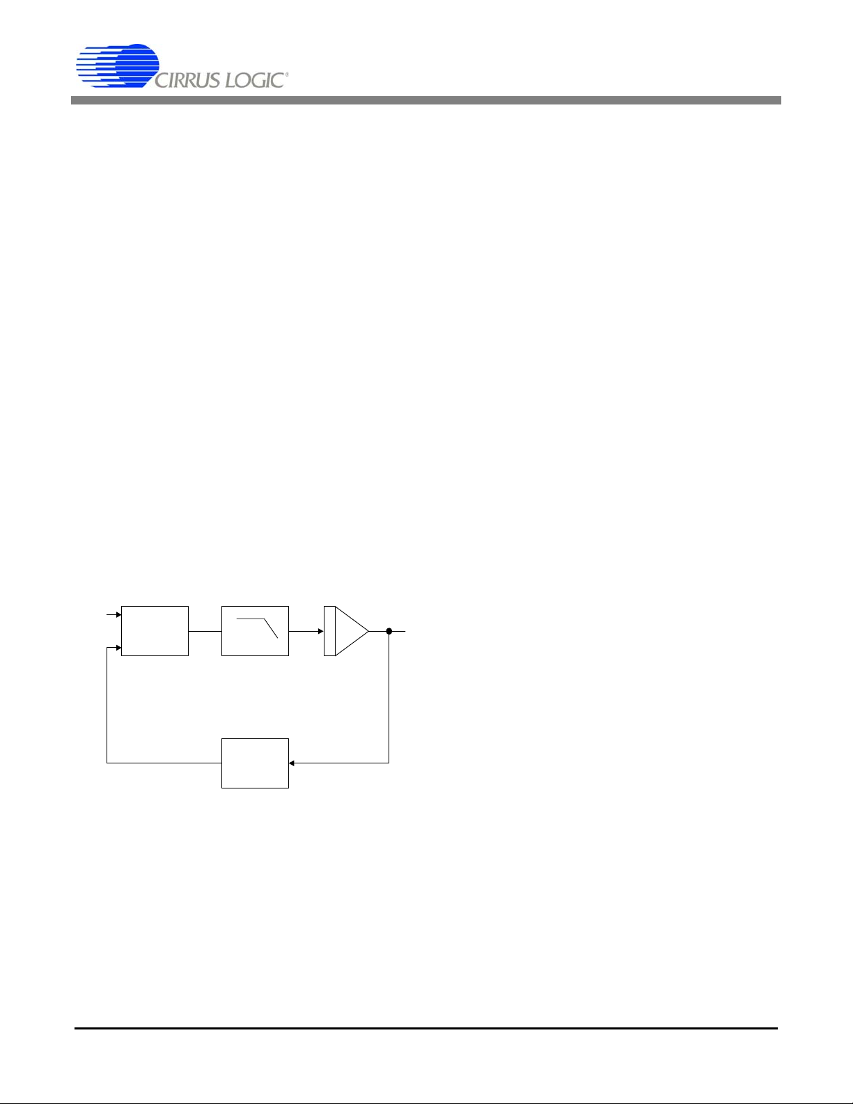
Figure 2. PLL Block Diagram
AN339
Beyond those listed in the table, several other no table enhancements are available in the CS8416:
There are a number of other differences between the CS8 413/14 and the CS8416 that a designer con sidering a transition from the CS8413/14 to the CS8416 should be aware of. For reference, a list of some of the more significant
differences is included in Section9.1 on page10.
3. BASICS OF CLOCK RECOVERY
The purpose of a S/PDIF receiver is to convert a 1-wire S/PDIF inpu t signal containing both clock and d ata information into discrete serial audio clock and data signals. A phase-locked loop (PLL) is used to derive a system clock
signal synchronous to the S/PDIF stream, and digital logic is used to decode the data.
In some limited applications, a S/PDIF receiver is used to source data into a purely digital system where clock jitter
needs to be only good enough to operate the internal digital components. However, the vast majority of systems with
a S/PDIF receiver also contain a D/A converter, an A/D converter, or a combination of the two, all being clocke d by
the PLL recovered system clock generated by the S/PDIF receiver. In these systems, the jitter performance of the
S/PDIF recovered clock is of extreme importance because it has a direct impact on the system’s analog audio performance.
clock frequency is adjusted by the error signal voltage until the ou tput clock frequency matches th e input. The feedback loop contains a frequency divider so that the output clock frequency can be a multiple of the input frequency.
The amount of jitter present on the recovered clock is dependent on the characteristics of the PLL that generates
the clock. Since the CS8413/14 and CS8416 have different PL Ls, the jitter on their recovered clocks is expected to
be different as discussed in the following section.
2 AN339REV1
As a result, an important qualifying factor for a
S/PDIF receiver is the performance of its r ecovered clock. If the S/PDIF receiver does not provide a low-jitter recovered clock, then any
converters that use the clock for sampling can be
expected to exhibit reduced performance as a result.
The basic block diagram of the PLL is shown in
Figure 2. The PLL uses a negative feedback loop
to compare the phase of the input clock to that of
the output clock. The resulting error voltage signal is low pass filtered and sent to an internal voltage-controlled oscillator (VCO). The VCO output
Page 3
AN339REV1
Time (seconds)
VCO
Frequency
(MHz)
Ideal VCO
Frequency
Phase Detector
Update Rate
VCO Jit t e r
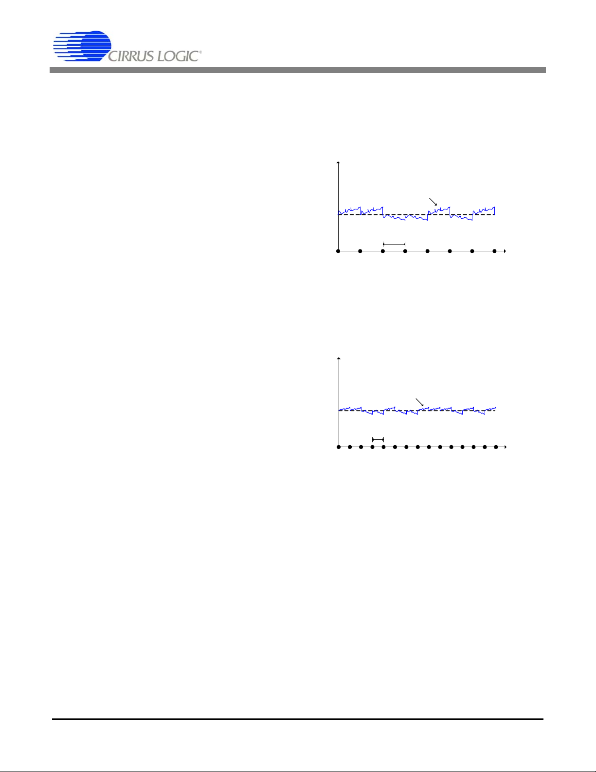
Figure 3. Slow Phase Detector Update Rate
Time (seconds)
VCO
Frequency
(MHz)
Ideal VCO
Frequency
Phase Detector
Update Rate
VCO Jitter
Figure 4. Fast Phase Detector Update Rate
AN339
4. CS8413/14 AND CS8416 CLOCK RECOVERY COMPARED
The primary difference between the CS8413/14 and CS8416 PLLs is foun d in the input source to each PLL’ s phase
detector block. In each of these devices, digital logic analyzes the incoming biphase enco ded S/PDIF stream to generate pulses that serve as the input to the pha se comparator. The frequency of th ese pulses is referred to as the
phase detector update rate.
The more often the phase detector is updated, the more
often the VCO output frequency is corrected to match the
frequency of the input S/PDIF signal. A slower update
rate allows the VCO frequency a greater degree of wander, leading to increased low frequency (audio-band) recovered clock jitter. See Figure 3 and Figure 4.
In practice, the CS8413/14 detector is updated once per
bit of the input S/PDIF signal; thus the update rate is da ta
dependent 64 times the input sample rate. With an update rate of this frequency, the CS8413/14 has good audio-band output jitter.
When the CS8416 was first released in 2002, its digital logic was designed to update its phase detector only once
per subframe of the S/PDIF input signal, or at 2 times the input sample rate. This was done as a measur e desig ned
to support 192 kHz sample rates and to reduce data dependency. The unfortunate result of this slower update rate
was higher audio-band jitter present on the recovered master clock.
To address this issue and improve upon the CS8416 and
CS8413/14, in 2004 a new phase detector update rate
option was added to the CS8416.
When enabled, the newer update rate option causes the
phase detector to be updated on every edge of the biphase S/PDIF input signal; thus the update rate is data
dependent from 64 to 128 times the input sample rate.
This new detector lowers the audio-band r ecovered clock
jitter and results in improved converter performance.
It’s important to note that the maximum sample rate is
limited to 108 kHz in this newer mode. The different detector modes in the CS8416 are selected by the Phase Detector Update Rate (PDUR) control. PDUR set low (‘0’)
selects the original and slower update rate, while PDUR set high (‘1’) selects the new fast update rate. The PDUR
setting can be accessed at start-up through the TX pin in hardware mode, or in register 00h in software mode.
Since the CS8416 with PDUR = 1 has the same update rate or faster than the CS8413/14, the CS8416 is expected
to have lower audio-band recovered clock jitter. Section 5 below details the results of jitter measurement tests that
empirically support this conclusion.
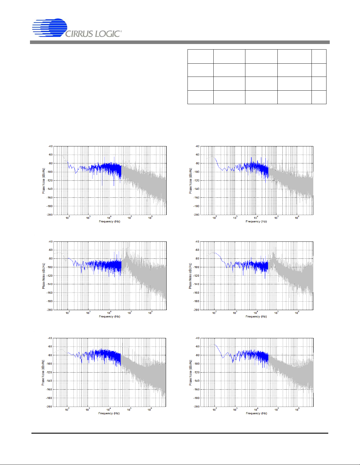
5. MEASURED JITTER COMPARISON
Although there are several d ifferent jitt er spe cification s used to quantify the jitter present on a clock signal (period,
cycle-to-cycle, etc.), they are not all useful for correlating measured jitter to the THD+N performance of an audio
converter that uses the measured clock signal to drive its sampling circuits.
The best jitter specification for this correlation is ‘baseband jitter’ as defined in section 3.4.2 of AES-12id-2006. A
baseband jitter measurement band-passes the measured jitter signal, calculating the jitte r amplitude over a frequency band from 100 Hz to 40 kHz. Jitter outside of this frequency band is said to have no effect on the THD+N performance of an audio converter because the resulting modulation tones will either be psycho-acoustically masked (jitter
less than 100 Hz) or higher than the upper limit of the 20 kHz audio band (jitter greater than 40 kHz).
AN339REV1 3
Page 4
AN339REV1
Sample
Rate
CS8414
-
CS8416
PDUR=1
CS8416
PDUR=0 Unit
48 kHz 158.5
(Figure 5)
122.57
(Figure 7)
531.41
(Figure 9)
ps
96 kHz 1 11.01
(Figure 6)
45.278
(Figure 8)
212.35
(Figure 10)
ps
192 kHz - - 215.43
(Figure 11)
ps
Table 2. Baseband Jitter - Summary
Figure 5. CS8414 MCK Phase Noise
Fs = 48 kHz
Figure 6. CS8414 MCK Phase Noise
Fs = 96 kHz
Figure 7. CS8416 RMCK Phase Noise
Fs = 48 kHz, PDUR = 1
Figure 8. CS8416 RMCK Phase Noise
Fs = 96 kHz, PDUR = 1
Figure 9. CS8416 RMCK Phase Noise
Fs = 48 kHz, PDUR = 0
Figure 10. CS8416 RMCK Phase Noise
Fs = 96 kHz, PDUR = 0
AN339
Each receiver, including both of the CS8416 phase detector update modes, was tested with input S/PDIF sample
rates at common values of 48 kHz and 96 kHz. Additionally, the CS8416 was tested at 192 kHz with PDUR = 0.
The resulting baseband jitter measurement data is presented in Table 2. Phase noise plots showing the measured jitter signal on the receivers’ recovered clocks are displayed
in Figures 5 through 11. Refer to Section 9.2 for detailed
test set-up information and diagrams.
The highlighted portions of each plot denote the 100 Hz to 40 kHz bandwidth specified by the AES-12id-2006 baseband jitter definition. As the definition suggests, the magnitude o f the hig hlighted portion of the plots corr elate to audio-band converter THD+N performance. Thus, the lower the magnitude, the better the converter performance.
4 AN339REV1
Page 5

AN339REV1
Figure 11. CS8416 RMCK Phase Noise
Fs = 192 kHz, PDUR = 0
AN339
The measurements show the CS8416 has less baseband
jitter than the CS8414 when PDUR = 1. While the plots
also indicate that the CS8416 has more jitter at higher frequencies, as suggested by AES-12id-2006 and confirmed
by the measurements to be shown in Section 6, this high
frequency jitter does not affect audio converter THD+N
performance.
It can also be seen that the CS8416 has higher baseband
jitter when PDUR = 0; this is due to its slower phase detector update rate in this mode. As an alternate illustration
of this point, notice that the baseband jitter is reduced for
all three receiver cases when the sample rate is increased. This is an indication that a faster phase detector
update rate results in reduced low frequency VCO noise on the recovered clock.
6. MEASURED CONVERTER PERFORMANCE COMPARISON
An alternate, and arguably more tangible way to evaluate the impact of the recovered clock jitter improvement provided by the CS8416 would be to simply measure the analog performance of a D/A converter clocked by the receiver’s recovered clock. The results from a few of these tests have been included to provide an example of how the
improvements made in the CS8416 will benefit a real-world audio application.
From a high-level, it’s easy to see that the improved jitter performance results in better THD+N performance of the
converter; see Table 3. Detailed plots and summary data can be found in the next few sections. These represent
the most common and critical analog performance metrics that can be expected to be affected by clock jitter.
The CS4398 high-performance D/A converter was used as the audio source for each measurement. Three common
sample rates were tested for each measurement: 48 kHz, 96 kHz, and 192 kHz. Since the CS8414 cannot accept a
sample rate of 192 kHz, performance data for the CS8414 operation at 48 kHz is used as a comparison baseline for
the plots demonstrating the CS8416 operation at 192 kHz.
Refer to Section 9.2 for detailed test set-up information and diagrams.
6.1 THD+N Measurements
Table 3 summarizes the performance differences, which are clearly most notable at 18 kHz. The plots that
follow show that the THD+N performance degrades as the signal amplitude and frequency are increased.
As predicted by the baseband jitter values in Section 5, the converter’s performance improves as the sample
rate is increased from 48 kHz to 96 kHz when sourced by either receiver. It’s also noteworthy that the performance with the CS8416 and PDUR = 0 at a sample rate of 192 kHz is comparable to the performance
with the CS8414 at a sample rate of 48 kHz. This shows that using the extended sample rate range of the
CS8416 doesn’t come at the expense of per fo rm anc e relative to th e be nc hm a rk se t by the CS84 1 4.
Fundamental
Frequency
997 Hz 48 kHz -106.97 -106.97 -105.53 dBr 12
997 Hz 96 kHz -106.96 -106.96 -106.77 dBr 14
997 Hz 192 kHz - - -107.57 dBr 16
18 kHz 48 kHz -99.21 -101.17 -90.06 dBr 12
18 kHz 96 kHz -103.33 -110.27 -97.59 dBr 14
18 kHz 192 kHz - - -98.50 dBr 16
Sample
Rate
CS8414 THD+N-CS8416 THD+N
PDUR=1
CS8416 THD+N
PDUR=0 Unit Figure
Table 3. THD+N Summary
AN339REV1 5
Page 6

AN339REV1
-130
-60
-125
-120
-115
-110
-105
-100
-95
-90
-85
-80
-75
-70
-65
d
B
r
A
20 20k50 100 200 500 1k 2k 5k 10k
Hz
CS8414
CS8416 PDUR =0
CS8416 PDUR =1
-130
-60
-125
-120
-115
-110
-105
-100
-95
-90
-85
-80
-75
-70
-65
d
B
r
A
-120 +0-100 -80 -60 -40 -20
dBFS
CS8414
CS8416 PDUR =0
CS8416 PDUR =1
Figure 12. THD+N vs Frequency - 0 dBFS
Fs = 48 kHz
Figure 13. THD+N vs Amplitude - 18 kHz
Fs = 48 kHz
-130
-60
-125
-120
-115
-110
-105
-100
-95
-90
-85
-80
-75
-70
-65
d
B
r
A
20 20k50 100 200 500 1k 2k 5k 10k
Hz
Figure 14. THD+N vs Frequency - 0 dBFS
Fs = 96 kHz
CS8414
CS8416 PDUR =0
CS8416 PDUR =1
-130
-60
-125
-120
-115
-110
-105
-100
-95
-90
-85
-80
-75
-70
-65
d
B
r
A
-120 +0-100 -80 -60 -40 -20
dBFS
CS8414
CS8416 PDUR =0
CS8416 PDUR =1
Figure 15. THD+N vs Amplitude -18 kHz
Fs = 96 kHz
-130
-60
-125
-120
-115
-110
-105
-100
-95
-90
-85
-80
-75
-70
-65
d
B
r
A
20 20k50 100 200 500 1k 2k 5k 10k
Hz
Figure 16. THD+N vs Frequency - 0 dBFS
Fs = 192 kHz
CS8414 (48 kHz)
CS8416 PDUR =0
-130
-60
-125
-120
-115
-110
-105
-100
-95
-90
-85
-80
-75
-70
-65
d
B
r
A
-120 +0-100 -80 -60 -40 -20
dBFS
CS8414 (48 kHz)
CS8416 PDUR =0
Figure 17. THD+N vs Amplitude - 18 kHz
Fs = 192 kHz
AN339
6 AN339REV1
Page 7

6.2 Full-Scale FFTs
-160
+0
-150
-140
-130
-120
-110
-100
-90
-80
-70
-60
-50
-40
-30
-20
-10
d
B
r
A
20 20k50 100 200 500 1k 2k 5k 10k
Hz
CS8414
CS8416 PDUR =0
CS8416 PDUR =1
Figure 18. FFT - 0 dBFS, 997 Hz
Fs = 48 kHz
-160
+0
-150
-140
-130
-120
-110
-100
-90
-80
-70
-60
-50
-40
-30
-20
-10
d
B
r
A
20 20k50 100 200 500 1k 2k 5k 10k
Hz
CS8414
CS8416 PDUR =0
CS8416 PDUR =1
Figure 19. FFT - 0 dBFS, 18 kHz
Fs = 48 kHz
-160
+0
-150
-140
-130
-120
-110
-100
-90
-80
-70
-60
-50
-40
-30
-20
-10
d
B
r
A
20 20k50 100 200 500 1k 2k 5k 10k
Hz
-160
+0
-150
-140
-130
-120
-110
-100
-90
-80
-70
-60
-50
-40
-30
-20
-10
d
B
r
A
20 20k50 100 200 500 1k 2k 5k 10k
Hz
CS8414
CS8416 PDUR =0
CS8416 PDUR =1
Figure 20. FFT - 0 dBFS, 997 Hz
Fs = 96 kHz
Figure 21. FFT - 0 dBFS, 18 kHz
Fs = 96 kHz
CS8414
CS8416 PDUR =0
CS8416 PDUR =1
-160
+0
-150
-140
-130
-120
-110
-100
-90
-80
-70
-60
-50
-40
-30
-20
-10
d
B
r
A
20 20k50 100 200 500 1k 2k 5k 10k
Hz
-160
+0
-150
-140
-130
-120
-110
-100
-90
-80
-70
-60
-50
-40
-30
-20
-10
d
B
r
A
20 20k50 100 200 500 1k 2k 5k 10k
Hz
Figure 22. FFT - 0 dBFS, 997 Hz
Fs = 192 kHz
Figure 23. FFT - 0 dBFS, 18 kHz
Fs = 192 kHz
CS8414 (48 kHz)
CS8416 PDUR =0
CS8414 (48 kHz)
CS8416 PDUR =0
FFTs of the 997 Hz and 18 kHz test cases are provided below. These show the differences in the tonal and
noise signatures of the converters when clocked from the CS8413/14 and the CS8416 in each PDUR mode.
AN339REV1
AN339
AN339REV1 7
Page 8

6.3 Dynamic Range Measurements
Sample
Rate
CS8414-CS8416
PDUR=1
CS8416
PDUR=0 Unit Figure
48 kHz -119.29 -118.64 -119.02 dBr 24
96 kHz -119.36 -119.18 -119.23 dBr 26
192 kHz - - -119.11 dBr 28
Table 4. A-Weighted Dynamic Range Summary
-160
+0
-150
-140
-130
-120
-110
-100
-90
-80
-70
-60
-50
-40
-30
-20
-10
d
B
r
A
20k 120k40k 60k 80k 100k
Hz
-160
+0
-150
-140
-130
-120
-110
-100
-90
-80
-70
-60
-50
-40
-30
-20
-10
d
B
r
A
20 20k50 100 200 500 1k 2k 5k 10k
Hz
Figure 24. FFT - -60 dBFS, 997 Hz
Fs = 48 kHz
Figure 25. FFT - No Input (w/ Dither)
Out of Band, Fs = 48 kHz
CS8414
CS8416 PDUR =0
CS8416 PDUR =1
CS8414
CS8416 PDUR =0
CS8416 PDUR =1
-160
+0
-150
-140
-130
-120
-110
-100
-90
-80
-70
-60
-50
-40
-30
-20
-10
d
B
r
A
20k 120k40k 60k 80k 100k
Hz
-160
+0
-150
-140
-130
-120
-110
-100
-90
-80
-70
-60
-50
-40
-30
-20
-10
d
B
r
A
20 20k50 100 200 500 1k 2k 5k 10k
Hz
Figure 26. FFT - -60 dBFS, 997 Hz
Fs = 96 kHz
Figure 27. FFT - No Input (w/ Dither)
Out of Band, Fs = 96 kHz
CS8414
CS8416 PDUR =0
CS8416 PDUR =1
CS8414
CS8416 PDUR =0
CS8416 PDUR =1
As discussed in section 5.2 of AES-12id-2006, jitter outside of the baseband frequency range can interact
with the shaped quantization noise of an audio converter and result in de creased dynamic range regar dless
of the level or frequency of the audio input signal. The level of dynamic range reduction is dependent upon
the out of band energy of the converter and the out of band jitter signal on its sample clock. Since the predominant multi-bit converter architectures of today produce less out of band energy than earlier converters
using a single-bit architecture, they can be expected to be less sensitive to out of band jitter.
The measurements reveal that there is little difference between the converter’s dynamic range when
sourced by each recovered clock source. There is a small reduction in dynamic range for the CS8416 and
PDUR = 1 case that can be attributed to the RMCK jitter in the ~100 kHz range as shown in Figure 7.
Table 4 summarizes the measurement results.
The plots that follow show the converter’s output
spectrum for each sample rate, both across the
audio band with a -60 dB input stimulus, and out
of the audio band with no input stimulus.
AN339REV1
AN339
8 AN339REV1
Page 9

AN339REV1
-160
+0
-150
-140
-130
-120
-110
-100
-90
-80
-70
-60
-50
-40
-30
-20
-10
d
B
r
A
20k 120k40k 60k 80k 100k
Hz
-160
+0
-150
-140
-130
-120
-110
-100
-90
-80
-70
-60
-50
-40
-30
-20
-10
d
B
r
A
20 20k50 100 200 500 1k 2k 5k 10k
Hz
Figure 28. FFT - -60 dBFS, 997 Hz
Fs = 192 kHz
Figure 29. FFT - No Input (w/ Dither)
Out of Band, Fs = 192 kHz
CS8414 (48 kHz)
CS8416 PDUR =0
CS8414 (48 kHz)
CS8416 PDUR =0
10
100
1000
40 60 80 100 120 140 160 180 200
Fs (kHz)
Baseband Jitter (ps)
-115
-110
-105
-100
-95
-90
-85
40 60 80 100 120 140 160 180 200
Fs (kHz)
18 kHz THD+N (dBr)
Figure 30. Baseband Jitter vs Samp le Rate
Figure 31. THD+N vs Sample Rate
CS8414
CS8416 PDUR =0
CS8416 PDUR =1
CS8414
CS8416 PDUR =0
CS8416 PDUR =1
AN339
7. JITTER MEASUREMENT TO DAC THD+N CORRELATION
The results presented in Section 5 show that the amount of baseband jitter present on the recovered master clock
of each receiver is reduced as the sample rate of the input S/PDIF signal is increased. This relationship is a direct
result of the increased phase detector update rate, which is proportional to the incoming sample rate.
Also, the results of Section 6 show that baseband jitter present on the recovered master clock has the most significant affect on the converter’s THD+N performance when its audio input signal level and frequency are both high.
Using this information, a simple test was devised to help correlate the level of baseband jitter to the DAC’s THD+N.
To do this, a S/PDIF signal with a fixed 0 dBFS, 18 kHz audio tone was transmitted into both receivers. The sa mple
rate of the S/PDIF signal was then varied, and both the recovered clock baseband jitter and the THD+N of the
CS4398 were measured at each sample rate step. The results are shown in Figure 30 and Figure 31 below.
The plots confirm the relationship between recovered clock baseband jitter and DAC THD+N. It can again be seen
that the baseband jitter and THD+N for the CS8416 when PDUR = 1 is better than that with the CS8414. For sample
rates greater than 96 kHz (up to 192 kHz), the jitter and THD+N for the CS8416 with PDUR = 0 is comparable to the
performance of the CS8414 with a sample rate of 48 kHz.
AN339REV1 9
Page 10

AN339REV1
• The CS8416 is not pin compatible with the
CS8413/14.
• The CS8416 receiver input pins are not RS-422
compliant; the receiver input absolute maximum
voltage range is ±12 V for the CS8413/14 and
-0.3 V to VL + 0.3 V for the CS8416.
• The typical VA and VD supply voltages are 5 V
for the CS8413/14 and 3.3 V for the CS8416.
• The external PLL filter component values are different between the CS8416 and CS8413/14.
• The recovered clock frequency provided when
the PLL is unlocked is approximately 3 MHz for
the CS8413/14 and approximately 375 kHz or
750 kHz for the CS8416, depending upon the
selected RMCK ratio.
• The CS8416 recovered clock output pin is not
active during reset.
• There are various differenc es between the devices’ C and U data framing implementations.
• The devices indicate their input sample rate differently.
• Although typical I²S, Left-Justified, and RightJustified formats are supported by the devices,
there are various differences in o ther suppor ted
serial audio output formats.
• The available controls over the state of the serial
data output during a receiver erro r condition are
different.
• There are various differences in the operation of
the devices’ error indication pins.
• Certain pins dedicated to the reporting of the C
data bits on the CS8414 are not available in the
CS8416’s hardware mode.
• The CS8413 is not directly register-compatible
with the CS8416 in software mode.
• The first five bytes of both channels’ C data are
register accessible in the CS8416’s software
mode, while the CS8413 allows sequential 1byte access to all 24-bits of a single channel’s C
data.
• There are various differences in the behavior of
the CS8413 and CS8416’s interrupt functions.
AN339
8. CONCLUSION
The CS8416 offers many improvements and features beyond th ose of the CS8413/14. One of the CS8416’s primary
improvements is the reduction of baseband jitter on its recovered master clock.
As shown through experiment, this jitter reduction improves the THD+N performance of a converter sourced by the
CS8416 when compared to the same converter sourced by the CS8413/14. This demonstration supports the
CS8416 as a performance-enhanced replacement for existing CS8413/14 designs.
9. APPENDIX
9.1 Other Differences Between CS8413/14 and CS8416
Aside from those listed in Section 2 on page 1, there are a number of other differences between the
CS8413/14 and the CS8416 that a designer considering a transition from the CS8413/14 to the CS8416
should be aware of. For refere nce, a list of some of the mor e significa nt diffe rences is included below. F or
complete details on any of these, please refer to each device’s datasheet.
9.2 System Set-Up
The data presented in this document is derived from measurements collected u sing one random ly selected
sample of each device. Measurements were taken at each device’s nominal voltage and at room temperature. Specifically, the CS8414 Revision A and the CS8416 Revision E were used.
To collect the audio performance data, the CS4398 high-performa nce DAC was chosen to demonstrate the
effect of each receiver’s output jitter. A single CDB4398 customer evaluation board was used to conduct
each test. The CS4398 FILT+ capacitor on the CDB4398 was increased from 100 µF to 1000 µF to ensure
a flat low-frequency THD+N response. The CS8414 located on the CDB4398 was used for all measurements sourced by the CS8414, and a CDB84 16 cus tom er evaluation board was used to drive the CS4398
10 AN339REV1
Page 11

AN339REV1
CDB4398
CS4398
U9
AOUTA
AOUTB
Tektronix
Oscilloscope
AP
SYS-2722
BALANCED
ANALOG
INPUT
AP
SYS-2722
S/P DIF
OUTPUT
J18
J27
J17
S/PDIF
INPUT
CS8414
U2
J8 J10 J9J6
Agilent E3631 A
Power Supp ly
GND +18V -18V+5V
Figure 32. CS8414 Test Setup
CDB8416
CS8416
J9
U19
CDB4398
CS4398
J12
U9
PCM INPUT
AOUTA
AOUTB
Tektronix
Oscilloscope
J18
PCM
OUTP UT
AP
SYS-2722
BALANCED
ANALOG
INPUT
AP
SYS-2722
S/P DIF
OUTPUT
J18
J27
J3 J4
S/PDIF
INPUT
J8 J10 J9J6
Agilent E3631A
Power Su pp lie s
+5V GND
GND +18V -18V+5V
Figure 33. CS8416 Test Setup
AN339
on the CDB4398 for all measurements sourced by the CS8416. Refer to the CDB4398 and CDB8416 data
sheets for more information on each evaluation board.
Block diagrams of each test set-up are shown in Figure 32 and Figure 33.
®
An Audio Precision
put signals for the receivers and to measure the analog output signals from the CS4398. Agilent
power supplies were used to power the evaluation boards.
®
A Tektronix
DPO7054 oscilloscope with JIT3 software was used to measure the jitter signal of the CS8414
and CS8416’s recovered master clocks. The sof tware was configured to generate pha se noise plots with no
averaging applied to produce the figures shown in Section 5. The phase noise integration function was used
to calculate the baseband jitter values shown in Table 2.
For each plot shown, the blue traces represent data ta ken us ing th e CS84 14 as the clock and da ta sou rce,
the green traces with the CS8416 and PDUR=1 as the clock and data source, and the red traces with the
CS8416 and PDUR=0 as the clock and data source. For clarity, only AOUTA is shown in the plots; no notable differences were seen between the CS4398 output channels.
(AP) SYS-2722 high-performance audio analyzer was used to generate the digital in-
®
E3631A
AN339REV1 11
Page 12

AN339REV1
Contacting Cirrus Logic Support
For all product questions and inquiries contact a Cirrus Logic Sales Representative.
To find one nearest you go to http://www.cirrus.com
IMPORTANT NOTICE
Cirrus Logic, Inc. and its subsidiaries (“Cirrus”) believe that the information contained in this document is accurate and reliable. However, the information is subject
to change without noti ce an d is pro vided “AS I S” witho ut war rant y of an y kind (expr ess or impl ied ). Cust omer s are ad vise d to ob tain the latest version of relevant
information to verify, before placing orders, that in formation be ing relied on is current and comp lete. All products are sold subject to the terms and con ditions of sale
supplied at the time of order acknowledgment, including those pertaining to warranty, indemnification, and limitation of liability. No responsibility is assumed by
Cirrus for the use of this information, including use of this information as the basis for manufacture or sale of any items, or for infringement of patents or other rights
of third parties. This document is the property of Cirrus and by furn ishing this information, Cirr us grants no license, express or implied under any patents, mask work
rights, copyrigh ts, tra demark s, tr ade s ecret s or ot her in te lle ctua l pr oper ty righ ts. Cir rus owns t he copy rig hts as soc iat ed wit h th e in for mati on co ntai ned h ere in a nd
gives consent for copies to be made of the information only for use within your organization with respect to Cirrus integrated circuits or other products of Cirrus. This
consent does not extend to other copying such as copying for general distribution, advertising or promotional purposes, or for creating any work for resale.
CERTAIN APPLICATIONS USING SEMICONDUCTOR PRODUCTS MAY INVOLVE POTENTIAL RISKS OF DEATH, PERSONAL INJURY, OR SEVERE PROPERTY OR ENVIRONMENTAL DAMAGE (“CRITICAL APPLICATIONS”). CIRRUS PRODUCTS ARE NOT DESIGNED, AUTHORIZED OR WARRANTED FOR
USE IN PRODUCTS SURGICALLY IMPLANTED INTO THE BODY, AUTOMOTIVE SAFETY OR SECURITY DEVICES, LIFE SUPPORT PRODUCTS OR OTHER
CRITICAL APPLICATIONS. INCLUSION OF CIRRUS PRODUCTS IN SUCH APPLICATIONS IS UNDERSTOOD TO BE FULLY AT THE CUSTOMER'S RISK
AND CIRRUS DISCLAIMS AND MAKES NO WARRANTY, EXPRESS, STATUTORY OR IMPLIED, INCLUDING THE IMPLIED WARRANTIES OF MERCHANTABILITY AND FITNESS FOR PARTICULAR PURPOSE, WITH REGARD TO ANY CIRRUS PRODUCT THAT IS USED IN SUCH A MANNER. IF THE CUSTOMER
OR CUSTOMER'S CUSTOMER USES OR PERMITS THE USE OF CIRRUS PRODUCTS IN CRITICAL APPLICATIONS, CUSTOMER AGREES, BY SUCH USE,
TO FULLY INDEMNIFY CIRRUS, ITS OFFICERS, DIRECTORS, EMPLOYEES, DISTRIBUTORS AND OTHER AGENTS FROM ANY AND ALL LIABILITY, INCLUDING ATTORNEYS' FEES AND COSTS, THAT MAY RESULT FROM OR ARISE IN CONNECTION WITH THESE USES.
Cirrus Logic, Cirrus, and the Cirrus Logic logo d esigns are tra demarks o f Cirrus Logic, In c. All other brand and pr oduct name s in this do cument m ay be trad emarks
or service marks of their respective owners.
Agilent is a registered trademark of Agilent Techno log ie s, Inc.
Tektronix is a registered trademark of Tektronix, Inc.
Audio Precision and the AP logo design are re giste re d trad emarks of Audio Precision, Inc.
AN339
9.2.1 Test Conditions
For all tests, unless otherwise state d: CS4398 VA = VREF = VD = VLS = VLC = 5 V; PCM data is 24 bit
2
S format; 22 Hz to 20 kHz measurement bandwidth for THD+N and dynamic range values. The unit
I
“dBr” is dB referenced to the measured 997 Hz full scale output voltage of the CDB4398, which was measured at 2.41 V
VA = VD = 5 V. CS8416 VA = VD = 3.3 V; VL = 5 V. The bin width is 2 Hz for all of the FFT plots, with the
exception of Figures 25, 27 and 29, which have a bin width of 8 Hz.
10.REFERENCES
1. Audio Engineering Society AES-12id-2006: “AES Information Document for digital audio measurements Jitter performance specifications,” May 2007.
11.REVISION HISTORY
Revision Date Changes
REV1 JUL 2009 Initial Release
. The S/PDIF input signal amplitude is 0.5 Vpp with 24-bit resolution. CS8414
RMS
12 AN339REV1
 Loading...