

Page 1
AN331
Increasing ADC Dynamic Range with Channel Summation
by
Steve Green
1. Introduction
A commonly used technique to increase the system dynamic range of audio converters is to operate two converter
channels in parallel with the same signal and sum the outputs. The summation of the correlated signals creates a
6 dB increase in signal level while the summation of the uncorrelated noise sources increases the noise level by
only 3 dB. This summation effectively results in a 3 dB increase in dynamic range compar ed to each individual channel. This technique is most commonly associat ed w ith digit al- to -ana lo g co nve r ter s bu t is als o ap p licab le to an alo g to-digital converters; as presented at the 87
A/D Converter, with 19-bit Mono Application Example” by Clifton Sanchez of Crystal Semiconductor. In the case of
an A/D converter, it may be necessary to divide each of the digital signals by two prior to sum mation to avoid signal
overload in the processor. This approach is shown in the eq uations below, where A repre sents the signal in channel
A, B the signal in channel B and e
e
= A/2 + B/2
o
is the summed signal.
0
th
AES Convention, “An 18-bit Dual Channel Oversampling Delta-Sigma
If A = B
eo = A/2 + A/2
e
Another approach, which achieves the identical mathematical results, is to invert one of the analog inputs prior to
conversion and perform a subtraction of the two independent digital outputs. The advantage of this approach is that
any common in-phase signal between the individual digital output signals that may be introduced during the conversion process (e
e
If B = - A
eo = ((A + eN) / 2)) - ((-A + eN) / 2)
e
Though applicable to any A/D converter summing channels, using either technique, to increase dynamic range is
generally implemented in applications requiring the ultimate in dyna mic range. As a result, this technique is generally
utilized with the highest performance A/D converters that are available. This application note will demonstrate an
implementation using the CS5381, which achieves 120 dB dynamic range for each individual channel in a standard
two-channel configuration, to achieve 123 dB dynamic range.
= A
o
) is cancelled in the subtraction. This approach is shown in the equations below.
N
= (A + eN) / 2) - (B+ eN) / 2)
o
= A
o
http://www.cirrus.com
Copyright © Cirrus Logic, Inc. 2008
(All Rights Reserved)
AUG ‘08
AN331REV1
1
Page 2
AN331
2. Implementation Requirements for the CS5381
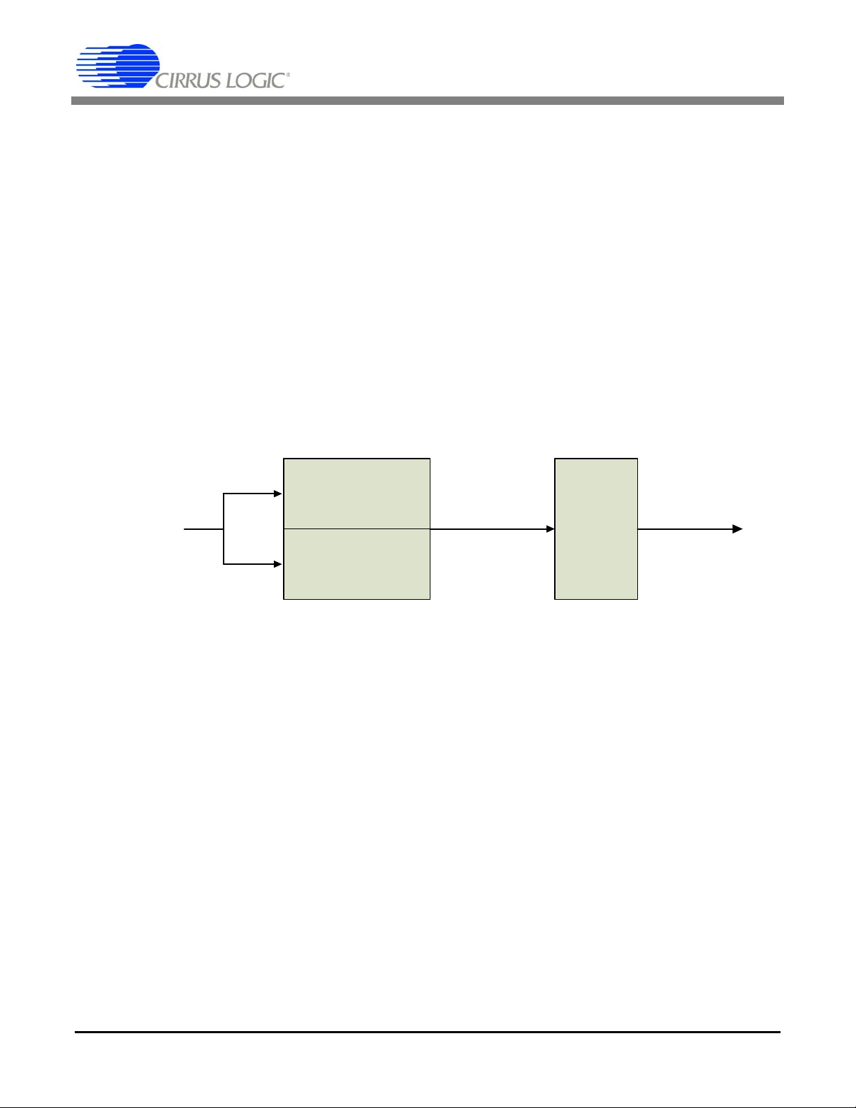
The block diagram shown in Figure 1 shows an implementation of the CS5381 A/D. Notice that the same analog
signal is applied to each of the A/D converters within the CS5381. The require d mathematical opera tion is th en performed in either a Digital Signal Processor (DSP) or Field Programmable Gate Array (FPGA).
It is very important to note that the addition (or subtraction) must be performed with synchronously sa mpled and time
aligned data pairs. Within the serial audio interface, the Left followed by Right cha nnel data pairs are synchronously
sampled data. However, the Right followed by Left channel data pairs are shifted in time by one sample period relative to each other and the addition or subtraction of these pairs will produce erroneous results. Please refer to the
Cirrus Logic application note AN282 “The 2-Channel Audio Interface: A Tutorial” for more information concerning
the serial audio interface and synchronously sampled data pairs.
Analog Input
CS5381
Right Channel A/D
Serial Audio Interface
CS5381
Left Channel A/D
Figure 1. Mono-Mode Block Diagram
Data
Processing in
DSP or FPGA
Mono-Channel
Output
2
Page 3
AN331
3. Recommended Analog Input Buffers for the CS5381 in Mono-Mode
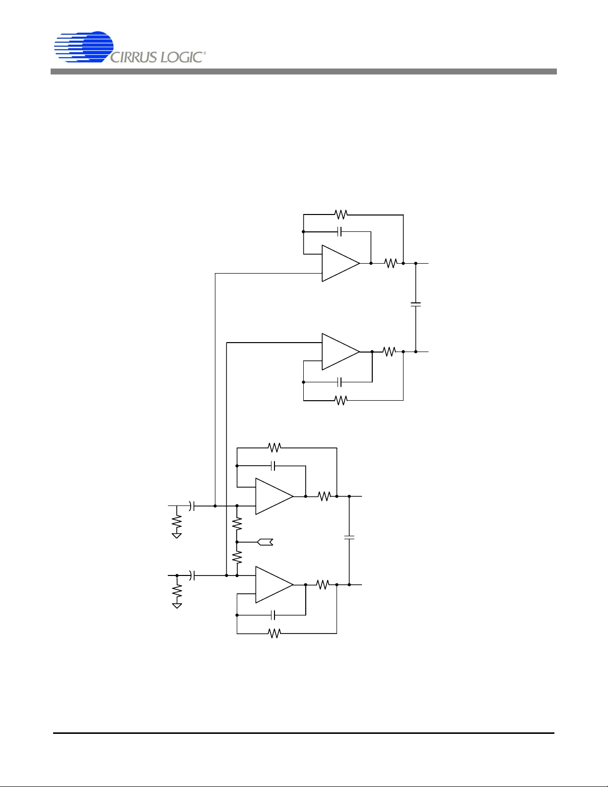
An implementation with the CS5381 requires separate inpu t buffer stages for th e differential analog in puts. A single
buffer driving both differential inputs has been shown to result in an unacceptable level of distortion. The recommended buffer topologies are near ly id entical to th at shown on the CS5381 evalua tio n board , CDB538 1. The schematic in Figure 2 is a suggested buffer implementation for the equation e
connection is routed to the AINR+ and the AINL+, and the AIN- connection is routed to the AINR- and the AINLwhich results in the signals being in-phase.
634 Ω
470 pF
COG
+
= A/2 + B/2. Notice that the AIN+
o
91 Ω
AINR+
COG
2700 pF
AIN+
AIN-
10 uF
100 kΩ
10 uF
100 kΩ
+
10 kΩ
10 kΩ
+
-
634 Ω
470 pF
COG
VQ
470 pF
COG
91 Ω
91 Ω
+
-
91 Ω
AINR-
470 pF
COG
634 Ω
AINL+
COG
2700 pF
AINL-
634 Ω
Figure 2. CS5381 Recommended Buffer Implementation for Non-inverting Configuration
3
Page 4

AN331
3.1 The Subtraction Approach
The schematic in Figure 3 is a suggested buffer implementation fo r the analog inversion with digital subtraction technique, e
inputs where the AIN+ connection is routed to the AINR- and the AINL+, and the AIN- connection is routed to the
AINR+ and the AINL-, as shown in Figure 3. This cross connection of the analog inputs results in the inversion of
the Right channel input relative to the Left channel.
= (A / 2) - (B / 2). The analog inversion can be easily implemented in the connections to the differential A/D
o
634 Ω
470 pF
COG
+
91 Ω
AINR-
COG
2700 pF
AIN+
AIN-
10 uF
100 kΩ
10 uF
100 kΩ
+
10 kΩ
10 kΩ
+
-
634 Ω
470 pF
COG
VQ
470 pF
COG
91 Ω
91 Ω
+
-
91 Ω
AINR+
470 pF
COG
634 Ω
AINL+
COG
2700 pF
AINL-
634 Ω
Figure 3. CS5381 Recommended Buffer Implementation for Channel Inversion
4
Page 5

AN331
4. Demonstrating the Technique
Assembling a test system to demonstrate this technique is a relatively simple matter using standard Cirrus Logic
evaluation boards and the Audio Precision System 2. The block diagram in Figure 4 shows a test set-up which includes the CDB5381 and CRD43530, the evaluation bo ards for the CS5381 A/D and the CS495 313 audio DSP. The
Audio Precision System 2 is the source of the analog signals as well as the analysis tool used to generate performance data and plots. The digital interconnections between the evaluation boards and the Audio Precision System 2
are the standard S/PDIF (IEC-60958) interface. The evaluation was performed at a 48 kHz sample rate but the performance improvement is valid at all sample rates.
Right Channel A/D
Audio
Pr ec is ion
System 2
Audio
Analyzer
Analog Inputs
CDB5381
Evaluation Board
SPD IF In te rfa c e
CRD49530
Cirrus CS495313
DSP
Left Channel A/D
Summ ed-Channe l Output
SPDIF In te rface
Figure 4. Test System Block Diagram
The A-weighted THD+N versus amplitude plots shown in Figure 5 clearly show the 3 dB performance impr ovement
that can be achieved with the channel summation technique. These plots were produced with the Audio Precision
generating equal amplitude and in-phase signals to both inputs of the CDB5381. Th e equation of e
performed in the DSP.
=A/2+B/2 was
o
4.1 The Subtraction Approach
The analog inversion with digital subtraction technique is also easily implemented with the test system. The only
differences are that the analog outputs of the Audio Precision are configured to generate an inverted signal to one
of the A/D inputs and the DSP is configured implement the subtraction, e
and there was no appreciable diff erence between the subtraction and the addition techniques with the CS5381 in
this test set-up. To a large degree, this is a result of the differential architecture of the CS5381. Implementation s
using different A/D architectures or systems designs have been shown to benefit from the subtr action technique and
produce improved results.
= A/2 - B/2. This configuration was tested
o
5
Page 6

AN331
100
-
-102
-104
-106
-108
-110
-112
d
-114
B
F
-116
S
-118
-120
-122
-124
-126
Stereo Mode
Mono Mode
-128
-130
-120 +0-110 -100 -90 -80 -70 -60 -50 -40 -30 -20 -10
dBr
Figure 5. A-Weighted THD+N versus Amplitude at 1 kHz
6
Page 7

Revision Date Changes
1 AUG 2008 Initial Release
AN331
7
Page 8

AN331
Contacting Cirrus Logic Support
For all product questions and inquiries contact a Cirrus Logic Sales Representative.
To find one nearest you go to http://www.cirrus.com
IMPORTANT NOTICE
Cirrus Logic, Inc. and its subsidiaries (“Cirrus”) believe that the information contained in this document is accurate and reliable. However, the information is subject
to change without noti ce an d is pro vided “AS I S” witho ut war rant y of an y kind (expr ess or impl ied ). Cust omer s are ad vise d to ob tain the latest version of relevant
information to verify, before placing orders, that info rmation be ing relied on is current and comp lete. All products are sold subject to the terms and con ditions of sale
supplied at the time of order acknowledgment, including those pertaining to warranty, indemnification, and limitation of liability. No responsibility is assumed by
Cirrus for the use of this information, including use of this information as the basis for manufacture or sale of any items, or for infringement of patents or other righ ts
of third parties. This document is the property of Cirrus and by furnish ing this information, Cirrus gran ts no license, express or implied under any patents, mask work
rights, copyrigh ts, tra demark s, trad e s ecret s or ot her in te llec tual pr opert y ri ght s. Cir rus owns t he copyri ght s as soci ated wit h t he i nfor mati on co nta ine d here in a nd
gives consent for copies to be made of the information only for use within your organization with respect to Cirrus integrated circuits or other products of Cirrus. This
consent does not extend to other copying such as copying for general distribution, advertising or promotional purposes, or for creating any work for resale.
CERTAIN APPLICATIONS USING SEMICONDUCTOR PRODUCTS MAY INVOLVE POTENTIAL RISKS OF DEATH, PERSONAL INJURY, OR SEVERE PROPERTY OR ENVIRONMENTAL DAMAGE (“CRITICAL APPLICATIONS”). CIRRUS PRODUCTS ARE NOT DESIGNED, AUTHORIZED OR WARRANTED FOR
USE IN PRODUCTS SURGICALLY IMPLANTED INTO THE BODY, AUTOMOTIVE SAFETY OR SECURITY DEVICES, LIFE SUPPORT PRODUCTS OR OTHER
CRITICAL APPLICATIONS. INCLUSION OF CIRRUS PRODUCTS IN SUCH APPLICATIONS IS UNDERSTOOD TO BE FULLY AT THE CUSTOMER'S RISK
AND CIRRUS DISCLAIMS AND MAKES NO WARRANTY, EXPRESS, STATUTORY OR IMPLIED, INCLUDING THE IMPLIED WARRANTIES OF MERCHANTABILITY AND FITNESS FOR PARTICULAR PURPOSE, WITH REGARD TO ANY CIRRUS PRODUCT THAT IS USED IN SUCH A MANNER. IF THE CUSTOMER OR CUSTOMER'S CUSTOMER USES OR PERMITS THE USE OF CIRRUS PRODUCTS IN CRITICAL APPLICATIONS, CUSTOMER AGREES, BY SUCH
USE, TO FULLY INDEMNIFY CIRRUS, ITS OFFICERS, DIRECTORS, EMPLOYEES, DISTRIBUTORS AND OTHER AGENTS FROM ANY AND ALL LIABILITY,
INCLUDING ATTORNEYS' FEES AND COSTS, THAT MAY RESULT FROM OR ARISE IN CONNECTION WITH THESE USES.
Cirrus Logic, Cirrus, and the Cirrus Logic logo designs are trademarks of Cirrus Logic, Inc. All other brand and product names in this document may be trademarks
or service marks of their respective owners.
8
 Loading...