

Page 1
AN314
Multiplexing the CS556x/7x/8x Delta-Sigma ADCs
1. INTRODUCTION
The CS556x/7x/8x devices represent a new generation of delta-sigma analog-to-digital converters that compete
with SAR (successive approximation register) converters, with some distinct advantages. The unique features of
these over-sampling converters allow them to be multiplexed at high speed across many input channels, because
every conversion produces a fully settled result. In this application note the similarities and differences between
SAR converters and the CS556x/7x/8x family of ADCs will be discussed as well as some design tips on choosing
the right multiplexer and input amplifiers to drive these ADCs.
2. COMPARING THE CS556X/7X/8X WITH A SAR
Typically SAR ADCs have been used in the past for any high-throughput multiplexed application. This is because
most delta-sigma converters require multiple conversions to fully settle. In other words, a large step change on the
input takes a considerable amount of time to be reflected accurately (settled) in the output of the digital filter. Most
delta-sigma converters use single-bit modulators and sample at kilohertz rates, and many samples are required as
input to the digital filter to achieve the required accuracy. The CS556x/7x/8x family of converters is unique in that
the modulator output is multi-bit and the sample rate is 8 MSps (megasamples per second). This, in combination
with a specially designed FIR filter that only takes a few clock cycles to compute a result, produces a converter that
can fully settle in a single conversion.
There are several distinct advantages of delta-sigma converters over SAR converters such as their superior DNL
(differential non-linearity) performance and excellent noise immunity. One of the main reasons for the increased
noise immunity is that the digital filter attenuates the out-of-band noise. However, a SAR ADC typically has a bandwidth much higher than Nyquist, and out-of-band noise can alias down into the pass band. Another reason is that
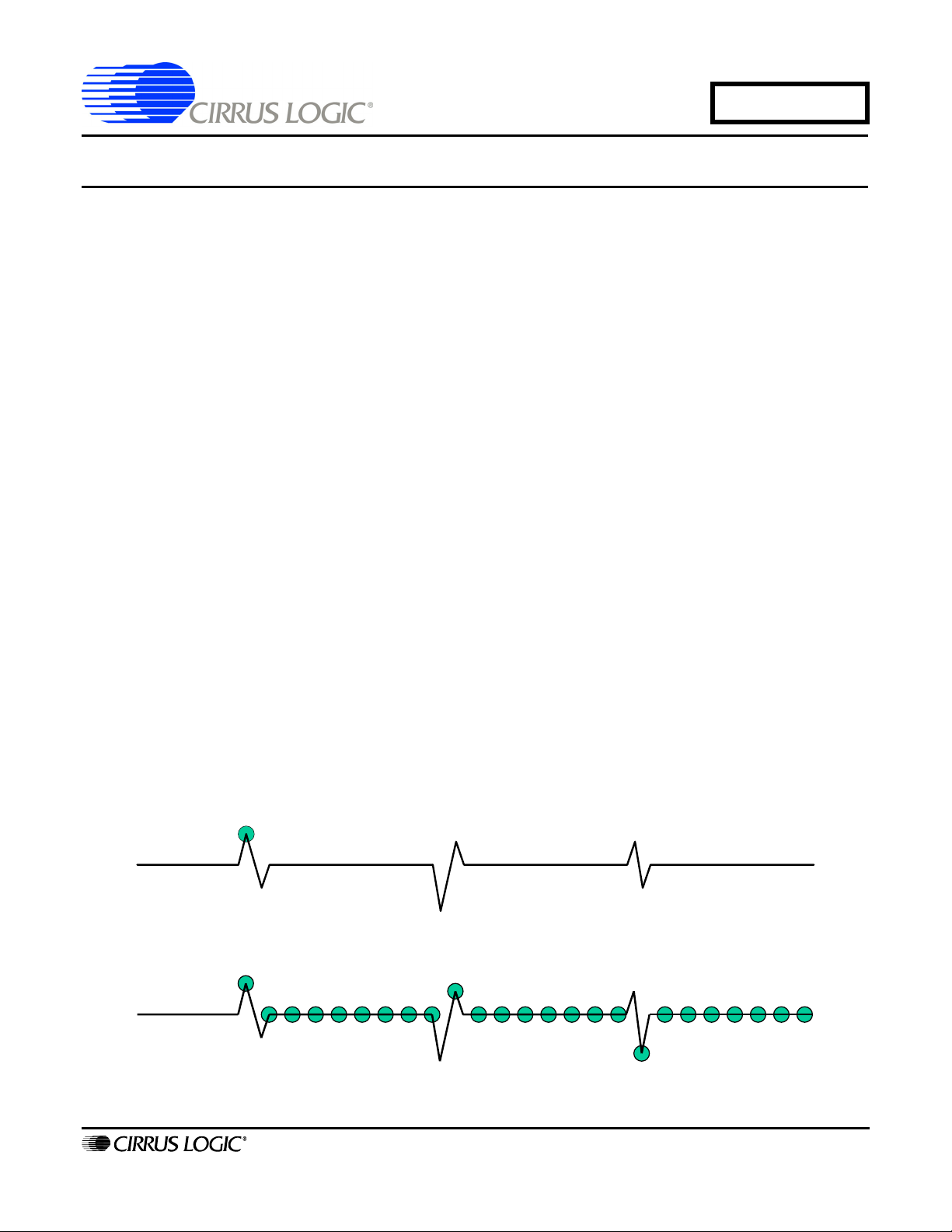
a SAR converter samples the input signal once per conversion (Figure 1a) while the delta-sigma converter averages
many samples per conversion (Figure 1b). As can be seen in Figure 1a, a noisy input signal (one with noise transients as illustrated) can result in significant errors within a SAR ADC unless multiple conversions are taken and
averaged in software. In Figure 1b, the delta-sigma converter does this internally in the digital filter resulting in a
conversion much less susceptible to transient noise.
Error
}
Noise
Figure 1a. SAR ADC Sampling (One Sample per Conversion)
Noise
Noise
Noise
Noise
Noise
http://www.cirrus.com
Figure 1b. Delta-Sigma ADC Sampling (Many Sample per Conversion)
Copyright © Cirrus Logic, Inc. 2007
(All Rights Reserved)
AUG ‘07
AN314REV1
Page 2
AN314
3. REQUIREMENTS FOR MULTIPLEXING THE CS556X/7X/8X
For higher-throughput in multiplexed applications, it is desirable for the converter to fully settle on each conversion.
In other words, the digital filter's output must accurately reflect the analog value on the input during the conversion.
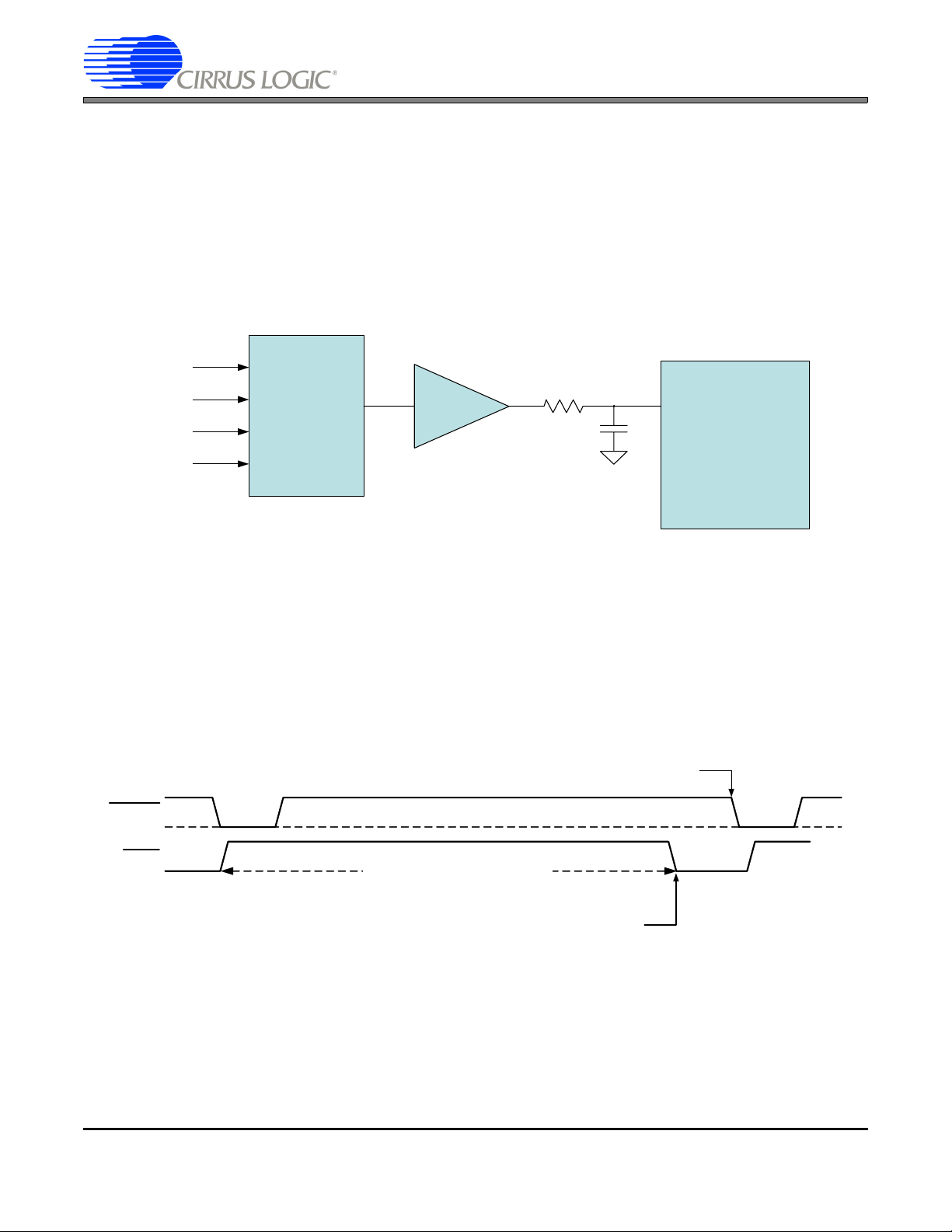
Additionally, the input multiplexer and any buffer amplifiers must be settled to the full accuracy of the converter before the samples are taken. This requires both the converter and the analog input circuitry to be fast settling. This
is especially true if any amplifier or anti-aliasing resistor and capacitor is placed between the multiplexer and the
ADC as illustrated in Figure 2. With a multiplexer it is possible for the ADC input to see a full-scale change from one
conversion to the next. Any amplifier, or RC time constant due to resistance and capacitance, between the multiplexer and the ADC must fully settle to the new value before the sampling begins.
AIN1
AIN2
AIN3
MUX
AMP
ADC
AIN4
Figure 2. Amplifier and Filter between Multiplexer and ADC
With high-throughput converters like the 50 kSps CS5560/61, 100 kSps CS5570/71, or the 200 kSps CS5580/81
the circuit must settle in less than 10 MCLK periods (625 nanoseconds). The multiplexer before a SAR converter
can be switched to the next channel after the conversion begins since the signal has already been sampled. However, many SAR ADC data sheets warn that a certain "quiet" period should be observed to prevent coupling of noise.
The CS556x/7x/8x requires that the multiplexer be switched at the end of the conversion, since it is taking multiple
samples of the input signal during the conversion (see Figure 3).
Analog Input must be settled here.
If CONV is held low , input must be
settled within 10 MCLKs after RDY falls.
CONV
RDY
See data sheet for specific timing
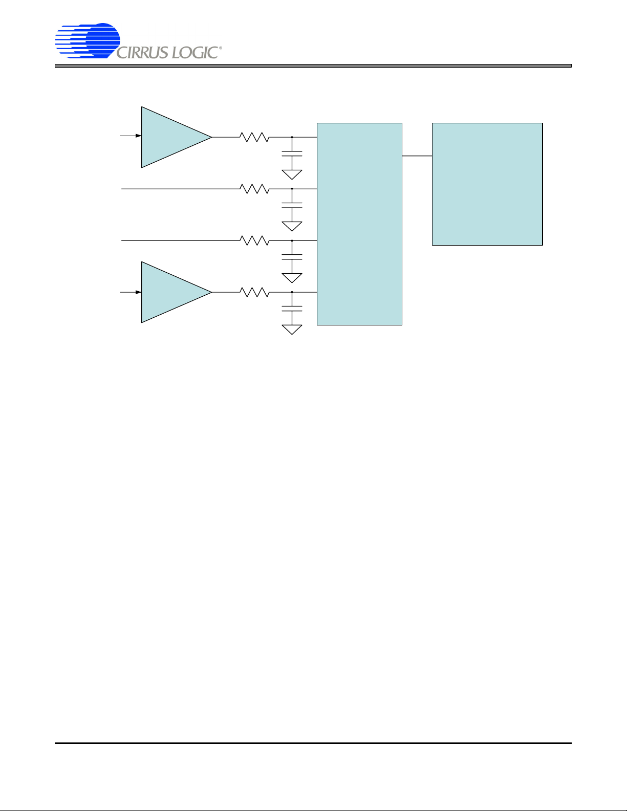
Therefore, an alternative should be considered where the amplifiers and anti-aliasing capacitors are on the input of
the multiplexer. This generally requires a multiplexer with very low “on” resistance but the benefits are that the amplifier(s) and RC networks do not have to settle from possible large step changes when the multiplexer switches to
another input. Figure 4 illustrates this arrangement.
2 AN314REV1
CS 5560/ 61 –304 MCLKs
CS 5570/ 71 –144 MCLKs
CS 5580/ 81 – 64 MCLKs
Switch MUX here
Figure 3. Multiplexer Timing Requirements
Page 3
AIN1
AN314
AIN2
ADC
MUX
AIN3
AIN4
Figure 4. Amplifier(s) and Filter(s) Placed Before Multiplexer
As illustrated, not every input may require an amplifier or buffer. This is because there is an on-chip buffer in the
CS556x/7x/8x. This rough charge buffer minimizes the sampling current on the input by charging the internal sample capacitor to a value very close to the input voltage using current from the supply pins rather than the input pin.
This results in much higher effective impedance on the analog input. Where the full-scale range needs to be
changed, an amplifier with gain or attenuation can be used.
4. SELECTING A MULTIPLEXER
There are several key parameters that need to be considered when selecting a MUX device. These include the “on”
resistance, on/off capacitance, and switching speed. The on resistance should be as low as possible in order to
assure that the input of the ADC fully settles on every sample. The inputs of modern converters consist of an analog
switch and a sample capacitor. For most SAR converters this sample capacitor (or array of capacitors) is in the
70 pF to 100 pF range and must be charged once per conversion. For the CS556x/7x/8x, the input sample capacitor
is only 4 pF but it is sampled once every 125 nanoseconds (8 MHz sample frequency). The CS556x/7x/8x also includes a rough-charge buffer which charges the sample capacitor to near its final value before switching the sample
capacitor directly to the input pin for the fine-sample period. This greatly increases the effective input impedance of
the device. However, this fine-sample period is only 20 nanoseconds out of each 125-nanosecond sample period,
so excessive resistance in the input path may result in inadequate settling. Another reason the on resistance should
be kept low is that the on resistance of a multiplexer is nonlinear across the full-scale range of the ADC and this may
result in distortion. The lower the on resistance, the less distortion will result from this nonlinearity. As a general
rule, an on resistance of less than 10 ohms should be used in order to minimize settling delays in charging the sample capacitance of the ADC.
The second parameter that should be considered is the channel capacitance or the on and off capacitance of the
multiplexer. Typically the inputs or source of a multiplexer have a capacitance of 5 pF to 20 pF when the switch is
open. However, when an input switch closes, additional capacitance is added from the other analog-switch channels that are part of the multiplexers output/drain. This capacitance typically increases as the number of multiplexer
inputs increase. For example, a 16-to-1 MUX will usually have a higher drain capacitance than an 8-to-1 MUX.
What needs to be considered here is that the output-channel capacitance will always be charged to the previously
AN314REV1 3
Page 4

AN314
selected input's voltage level and this charge will be dumped into the next input’s source when that switch closes.
If an op-amp or high-impedance source is used for the input to the MUX, there could be an issue with settling when
this charge is transferred through the switch. One of the functions of the anti-alias capacitor on the input side of the
MUX in Figure 3 is to provide a reservoir of charge to the switch-channel capacitance. This is another reason why
the on resistance of the MUX should be as low as possible – so the channel capacitance can be charged quickly.
However, there is an inverse relationship between on resistance and channel capacitance because low on resistance requires larger transistors and larger transistors result in higher channel capacitance. The following table
shows some examples of MUX devices along with their critical parameters. The devices grayed out are not recommended due to the parameters indicated.
Table 1: Critical Parameters of Typical Multiplexers
Part
Number
ADG706 1 16 50/14 2.5 13 200 1.8 to 5.5
ADG707 2 8 50/14 2.5 13 100 1.8 to 5.5
ADG787 2 2 22/6 2.5 16 40 1.8 to 5.5
ADG884 2 2 53/21 0.28 103 295 1.8 to 5.5
DG406 1 16 134/98 60 6 114 ±5 to ±20
DG407 2 8 134/98 60 6 57 ±5 to ±20
DG408 1 8 150/150 100 3 37 ±5 to ±20
DG409 2 4 150/150 100 3 25 ±5 to ±20
HI-506 1 16 250/250 180 10 62 ±15
HI-507 2 8 250/250 180 10 40 ±15
HI-508 1 8 250/250 180 10 27 ±15
HI-509 2 4 250/250 180 10 22 ±15
ISL43L220 2 2 12/5 0.23 115 224 1.1 to 4.5
MAX306 1 16 130/55 60 8 140 ±4.5 to ±20
MAX307 2 8 130/55 60 8 70 ±4.5 to ±20
MAX4617 1 8 7/4.5 8 5 32 2 to 5.5
MAX4618 2 4 7/4.5 8 5 21 2 to 5.5
MAX4635 2 2 12/5 2.5 9 32 1.8 to 5.5
# of
Poles
# of
Inputs
On/Off
Speed ns
On Res
Ohms
Off
Cap pF
On Cap
pF
Supply
Voltage
Notes:
1. Devices in gray are not recommended for this application due to the indicated parameters.
2. Parameters are typical values and are for comparative purposes only.
3. The manufacturer's data sheet should be referenced for min and max values
The third parameter to be considered when selecting a MUX is the switching speed. What needs to be considered
here is the total time from when the system selects another channel to when the conversion can begin. This includes
MUX turn-on time and analog circuitry settling time. For example, if it is desired to convert with the CS556x at its
maximum speed of 50 kSps (CONV
gins is 10 MCLKs (at 16 MHz) or 625 nanoseconds. This means that the MUX channel must change as RDY
and its turn on time and all analog settling must occur in less than 625 nanoseconds. If a MUX requires
250 nanoseconds to turn on, there is only 325 nanoseconds for the analog circuitry to settle. If more settling time
is required, the CONV
MUX channel is changed to ensure complete settling.
The type of multiplexer selected will depend upon whether the converter is a single-ended-input or a differentialinput ADC. The advantage of using a differential ADC rather than one with a single-ended input is an improvement
4 AN314REV1
pin timing can be delayed to slow down the conversion rate, allowing enough delay after the
held low), then from the time the RDY signal falls until the next conversion be-
falls
Page 5

AN314
of approximately 6 dB in the full-scale signal-to-noise ratio. This is because the full-scale input range of the differential input devices is twice that of the single ended devices. For example the CS5560/70/80 has a differential input
range of 8.192 volts (±4.096) while the CS5561/71/81 has a full-scale input range of 4.096 volts (±2.048). For an
equivalent internal noise, this means the full-scale input-to-noise ratio improves by 6 dB when using the differential
input devices. Of course, in order to take advantage of the differential device, the signal being converted needs to
be a true differential signal that utilizes the full-scale range. Otherwise, a single-ended-to-differential conversion circuit would need to be designed using a low-noise op-amp such as illustrated in Figure 5.
20k
20k
½ CS3004
-
±10.107 V
Single
Ended
Input
88.7k
10k
+
±4.096 V
20k
Diffe rentia l
Output
½ CS3004
-
+
Figure 5. Single-ended-to-differential Conversion Circuit
If the decision is made to use a differential input ADC then the MUX will need to be a dual-pole device. Otherwise,
for simpler implementations with less stringent noise performance requirements, a single-ended input device can
be used with a single-pole MUX.
AN314REV1 5
Page 6

AN314
5. SELECTING AN AMPLIFIER
If an amplifier is needed to change the full-scale range or to buffer the inputs and it is placed between the MUX and
the ADC, one of the most critical parameters will be settling time. However, as mentioned above, if the amplifier is
placed before the MUX (one on each input of the MUX where needed) this requirement is greatly relaxed. In thiscase, signal-to-noise, distortion, DC offset, and stability over temperature become the primary selection criteria for
most applications. Each application will determine which parameters are most critical so it becomes difficult to specify an op-amp and circuit configuration that will work in all situations. The CS3003 and CS3004 operational amplifiers will be suitable for many applications due to their excellent DC performance, moderate bandwidth, and low
noise.
6. OPTIMIZED CIRCUITS FOR MULTIPLEXING CS556X/7X/8X ADCs
The following are examples of circuits that optimize the performance of the CS556x/7x/8x family of high-throughput
ADCs for a number of general-purpose applications. Each circuit is followed by a brief circuit description with the
key selection criteria noted.
6 AN314REV1
Page 7

AN314
Figure 6. 2-input, Single-ended-to-differential, Multiple Input Range, Multiplexed System
In Figure 6, the differential device, CS5560, is multiplexed between two inputs which use single-ended-to-differential
conversion circuits. As illustrated, each of these circuits can be configured to attenuate or amplify the single-ended
input signal to use the full-scale range of the converter which is differentially ±4.096V. C4 is an optional capacitor
which can be used to attenuate out-of-band noise to improve overall noise performance. The corner frequency with
the components shown is 18 kHz. The 100 pF to 150 pF capacitors in the feedback of each amplifier are required
to compensate for the capacitive load of the 4700 pF capacitors on the inputs of the multiplexer. The 4700 pF capacitors provide a charge reservoir for the switched-channel capacitance of the multiplexer and also provide dynamic input current when the converter samples.
AN314REV1 7
Page 8

AN314
Figure 7. 8-input, Single-ended, Multiple Input Range, Multiplexed System
The circuit shown in Figure 7 is similar to the differential circuit except there is no need to convert the single-ended
input signal to differential. As mentioned previously, there will be a loss of approximately 6 dB in noise performance
using the single-ended input device, since the full-scale input is half that of the differential device. As illustrated, not
every input may need a buffer and if the source impedance is very low, better performance may be obtained without
a buffer. In order to maintain DC accuracy, the series resistance in the unbuffered inputs needs to be kept very low.
The key in this configuration is to keep the impedance between the ACOM pin of the ADC and the source signal as
low as possible. Any current flowing in this return path will result in errors since there is no common-mode rejection
with a single-ended device.
8 AN314REV1
Page 9

AN314
7. CONCLUSION
The CS556x/7x/8x family of devices offers an exceptional alternative to SAR devices in multiplexed applications.
Due to their digital filter with single-conversion settling, the input to the ADC can change from one end of full scale
to the other between conversions and still maintain full accuracy. Since delta-sigma converters have far superior
differential non-linearity (DNL) specifications and excellent noise performance, they provide a performance upgrade
path from conventional SAR ADCs. They also offer 24-bit resolution which is unattainable with SAR devices today.
AN314REV1 9
Page 10

REVISION HISTORY
Release Date Changes
REV1 AUG 2007 Initial Release
AN314
Contacting Cirrus Logic Support
For all product questions and inquiries, contact a Cirrus Logic Sales Representative.
To find the one nearest to you, go to http://www.cirrus.com
IMPORTANT NOTICE
Cirrus Logic, Inc. and its subsidiaries ("Cirrus") believe that the information contained in this document is accurate and reliable. However, the information is subject
to change without notice and is provided "AS IS" without warranty of any kind (express or implied). Customers are advised to obtain the latest version of relevant
information to verify, before placing orders, that information being relied on is current and complete. All products are sold subject to the terms and conditions of sale
supplied at the time of order acknowledgment, including those pertaining to warranty, indemnification, and limitation of liability. No responsibility is assumed by Cirrus
for the use of this information, including use of this information as the basis for manufacture or sale of any items, or for infringement of patents or other rights of third
parties. This document is the property of Cirrus and by furnishing this information, Cirrus grants no license, express or implied under any patents, mask work rights,
copyrights, trademarks, trade secrets or other intellectual property rights. Cirrus owns the copyrights associated with the information contained herein and gives consent for copies to be made of the information only for use within your organization with respect to Cirrus integrated circuits or other products of Cirrus. This consent
does not extend to other copying such as copying for general distribution, advertising or promotional purposes, or for creating any work for resale.
CERTAIN APPLICATIONS USING SEMICONDUCTOR PRODUCTS MAY INVOLVE POTENTIAL RISKS OF DEATH, PERSONAL INJURY, OR SEVERE PROPERTY OR ENVIRONMENTAL DAMAGE (“CRITICAL APPLICATIONS”). CIRRUS PRODUCTS ARE NOT DESIGNED, AUTHORIZED OR WARRANTED FOR USE
IN AIRCRAFT SYSTEMS, MILITARY APPLICATIONS, PRODUCTS SURGICALLY IMPLANTED INTO THE BODY, AUTOMOTIVE SAFETY OR SECURITY DEVICES, LIFE SUPPORT PRODUCTS OR OTHER CRITICAL APPLICATIONS. INCLUSION OF CIRRUS PRODUCTS IN SUCH APPLICATIONS IS UNDERSTOOD
TO BE FULLY AT THE CUSTOMER’S RISK AND CIRRUS DISCLAIMS AND MAKES NO WARRANTY, EXPRESS, STATUTORY OR IMPLIED, INCLUDING THE
IMPLIED WARRANTIES OF MERCHANTABILITY AND FITNESS FOR PARTICULAR PURPOSE, WITH REGARD TO ANY CIRRUS PRODUCT THAT IS USED
IN SUCH A MANNER. IF THE CUSTOMER OR CUSTOMER’S CUSTOMER USES OR PERMITS THE USE OF CIRRUS PRODUCTS IN CRITICAL APPLICATIONS, CUSTOMER AGREES, BY SUCH USE, TO FULLY INDEMNIFY CIRRUS, ITS OFFICERS, DIRECTORS, EMPLOYEES, DISTRIBUTORS AND OTHER
AGENTS FROM ANY AND ALL LIABILITY, INCLUDING ATTORNEYS’ FEES AND COSTS, THAT MAY RESULT FROM OR ARISE IN CONNECTION WITH
THESE USES.
Cirrus Logic, Cirrus, and the Cirrus Logic logo designs are trademarks of Cirrus Logic, Inc. All other brand and product names in this document may be trademarks
or service marks of their respective owners.
10 AN314REV1
 Loading...