

Page 1
AN313
CS556x / 7x / 8x:
Converting Output Data from Serial to Parallel
1. Introduction
The CS556X, CS557X, and CS558X series of high-throughp ut Delta-Sigma A/D conver ters output data in serial format. Some applications may require that data be available in parallel format. This application note will discuss how
to use common serial-to-parallel register ICs to provide parallel data output capability for these A/D converters.
Some A/D converters provide parallel outp ut data as an output option. While this makes for faster data transfer it
can introduce some possible com promises in the performa nce of the A/D conver ter. A parallel interface r equires
many more pins on the A/D than a seria l interface. This factor can increase the cost, but a larger concern should
be how a parallel interface can reduce performan ce. The data interface has many m ore connections via bond wires
to the semiconductor die. When the digital data on the digital bus is changing each bond wire acts as a radiator of
an electromagnetic field. This electromagnetic field can interfere with the performance of the converter. The dig ital
activity on the bus need not be due to the converter itself but may be caused by other peripherals using the same
bus. Many A/D converters that have parallel interfaces recommend that bus activity be stopped when a conversion
is performed, and that the data from the converter be read when the converter is not performing a conversion. Another option would be to provide a second set of latches outside the A/D to isolate the bus activity from being on the
digital output pins of the converter itself.
2. The CS556x/7x/8x
Cirrus Logic has chosen to offer the CS556X/7X/8X series of converters with only a serial interface. This reduces
the package pin count and also r educes the number of digi tal interface pins that can radiate noise onto the converter
die. The serial interface provides two different modes of operation. The serial port on the conver ter can oper ate in
either master mode, where the converter itself outputs the data according to its own timing (this mode is called the
SSC mode, synchronous self-clock mode). The second mode is where the serial port acts as a slave device to an
external controller, where the serial data is output from the port according to the clock provided by the external device (this mode is the SEC mode, synchronous external clock mode).
3. Serial-to-Parallel Conversion
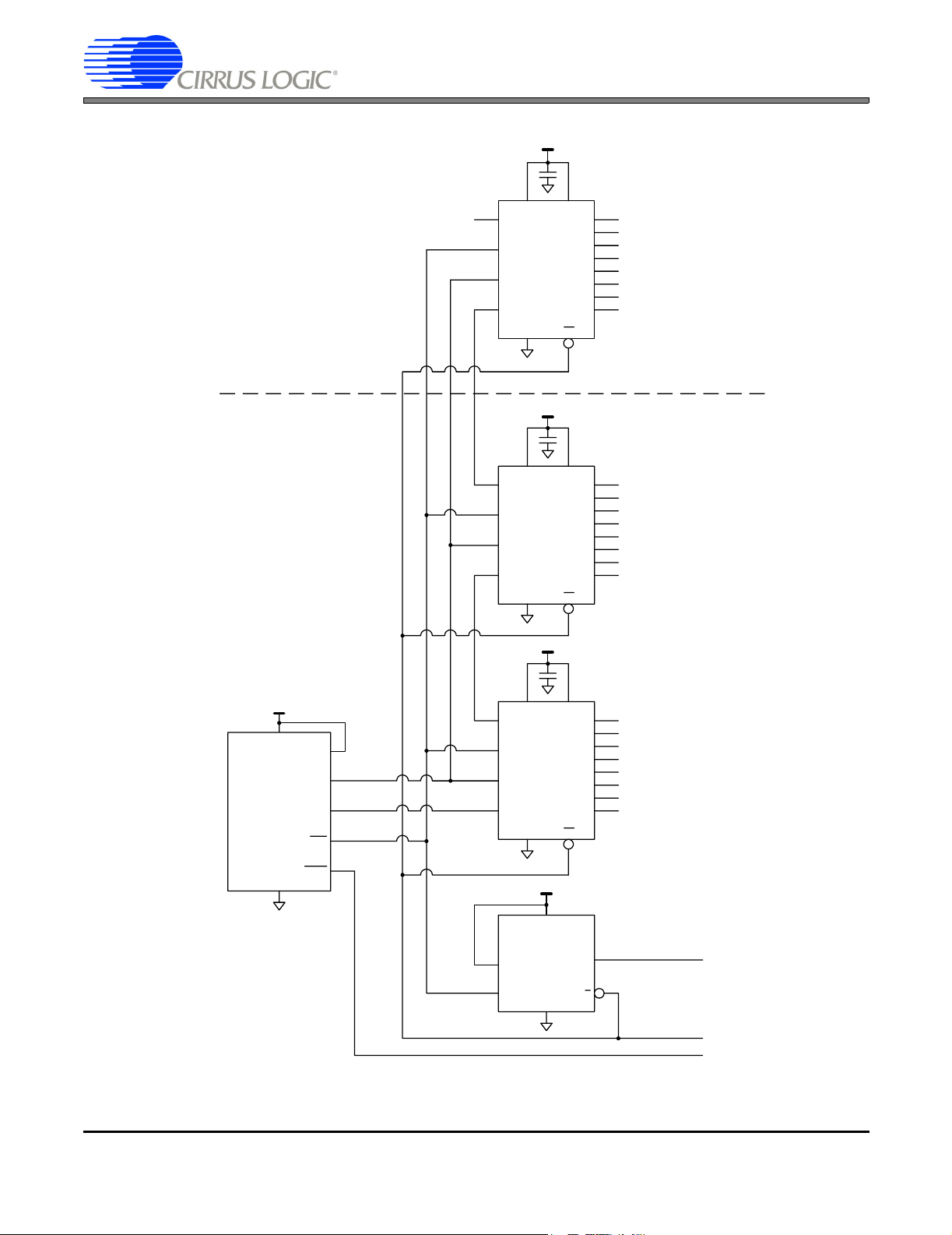
If an application requires a parallel interface to read the converter data, then the A/D can be configured in the SSC
serial port mode and directly interfaced to serial-to-parallel registers. Figure 1 illustrates the CS556x/7x/8x A/D converter interfaced to a set of 74VHC595 serial-to-parallel registers. The SMODE pin of the converter is tied to the
VL supply (tied high) to set the serial port mode of the converter into the SSC (master) mode. At the end of each
conversion the RDY
active. The data bits from SDO will be shifted into the first 74VHC595 register by the rising edges of SCLK. The
74VHC595 device holds eight bits of data. Multiple 74HVC595 devices are daisy-chained to provide either a 16bit parallel (two 74VHC595s) or a 24-bit parallel (three 74VHC595s) interface. The 74VHC595 has a tri-state outp ut
so the outputs of these devices can be attached to a multi-peripheral bus. The RDY
the bits from the converter have been shifted into the registers. When RDY
latch to provide a "data ready" signal at its Q output. When the read signal from the system goes low, the outputs
of the 74VHC595 devices will come out of tri-state and place their data on the bus. The falling read signal will also
clear the "data ready" signal back to a zero at the Q output of the NC75Z175 latch.
output from the converter will transition low, and the SCLK and the SDO outputs will become
signal will return high when all
transitions high it will set the NC75Z175
http://www.cirrus.com
Copyright © Cirrus Logic, Inc. 2007
(All Rights Reserved)
JUN ‘07
AN311REV1
Page 2
PWR
DOUT
74VHC595
LATCH CLK
SHIFT CLK
DIN
GND
AN313
VL
RST
OE
QH
QG
QF
QE
QD
QC
QB
QA
D23
D22
D21
D20
D19
D18
D17
D16
24-Bit Data
VL
VL
CS556x
CS557x
CS558x
SMODE
SCLK
SDO
RDY
PWR
DOUT
74VHC595
LATCH CLK
SHIFT CLK
DIN
GND
PWR
DOUT
74VHC595
LATCH CLK
SHIFT CLK
DIN
GND
VL
RST
QH
QG
QF
QE
QD
QC
QB
QA
OE
VL
RST
QH
QG
QF
QE
QD
QC
QB
QA
OE
16-Bit Data
D15
D14
D13
D12
D11
D10
D9
D8
D7
D6
D5
D4
D3
D2
D1
D0
CONV
VLR
VL
PWR
NC75Z175
D
CL C
GND
Q
Data Ready
Read
Convert
Figure 1. CS556x/7x/8x Driving Serial-to-Parallel Registers
2 AN311REV1
Page 3

AN313
Figure 2 shows the timing of the RDY/, SCLK, and SDO signals from the A/D converter.
RDY
SCLK(o)
LSB
SDO
MSB MSB–1
Figure 2. CS556x/7x/8x Serial Data Output Signals
LSB+1
4. Minimizing EMI
There are applications where output data from a converter must pass via a cable to another circuit board assembly.
If this is required, each active signal should have its own ground wire “partner”. On a connecter, such as a dual row
stake header, each active signal should be paired with a ground signal. Any connecting cable should be constructed
from twisted pair ribbon cable where each active signal has its own ground “partner” which is the other wire in the
twisted pair. This minimizes radiated noise and reduces the likelihood that radiated noise will interfere with converter
performance. It aslo enhances the likelihood that the system will pass any EMC (electromagnetic compatibility) requirements.
This wiring method is illustrated in Figure 3.
D23
D22
D21
D1
D0
Figure 3. Recommended Connector & Cable Configuration
AN311REV1 3
Page 4

Revision History
Release Date Changes
REV1 JUN 2007 Initial Release
AN313
Contacting Cirrus Logic Support
For all product questions and inquiries, contact a Cirrus Logic Sales Representative.
To find the one nearest to you, go to http://www.cirrus.com
IMPORTANT NOTICE
Cirrus Logic, Inc. and its subsidiaries ("Cirrus") believe that the information contained in this document is accurate and reliable. However, the information is subject
to change without notice and is provided "AS IS" without warranty of any kind (express or implied). Customers are advised to obtain the latest version of relevant
information to verify, before placing orders, that information being relied on is current and complete. All products are sold subject to the terms and conditions of sale
supplied at the time of order acknowledgment, including those pertaining to warranty, indemnification, and limitation of liability. No responsibility is assumed by Cirrus
for the use of this information, including use of this information as the basis for manufacture or sale of any items, or for infringement of patents or other rights of third
parties. This document is the property of Cirrus and by furnishing this information, Cirrus grants no license, express or implied under any patents, mask work rights,
copyrights, trademarks, trade secrets or other intellectual property rights. Cirrus owns the copyrights associated with the information contained herein and gives consent for copies to be made of the information only for use within your organization with respect to Cirrus integrated circuits or other products of Cirrus. This consent
does not extend to other copying such as copying for general distribution, advertising or promotional purposes, or for creating any work for resale.
CERTAIN APPLICATIONS USING SEMICONDUCTOR PRODUCTS MAY INVOLVE POTENTIAL RISKS OF DEATH, PERSONAL INJURY, OR SEVERE PROPERTY OR ENVIRONMENTAL DAMAGE (“CRITICAL APPLICATIONS”). CIRRUS PRODUCTS ARE NOT DESIGNED, AUTHORIZED OR WARRANTED FOR USE
IN AIRCRAFT SYSTEMS, MILITARY APPLICATIONS, PRODUCTS SURGICALLY IMPLANTED INTO THE BODY, AUTOMOTIVE SAFETY OR SECURITY DEVICES, LIFE SUPPORT PRODUCTS OR OTHER CRITICAL APPLICATIONS. INCLUSION OF CIRRUS PRODUCTS IN SUCH APPLICATIONS IS UNDERSTOOD
TO BE FULLY AT THE CUSTOMER’S RISK AND CIRRUS DISCLAIMS AND MAKES NO WARRANTY, EXPRESS, STATUTORY OR IMPLIED, INCLUDING THE
IMPLIED WARRANTIES OF MERCHANTABILITY AND FITNESS FOR PARTICULAR PURPOSE, WITH REGARD TO ANY CIRRUS PRODUCT THAT IS USED
IN SUCH A MANNER. IF THE CUSTOMER OR CUSTOMER’S CUSTOMER USES OR PERMITS THE USE OF CIRRUS PRODUCTS IN CRITICAL APPLICATIONS, CUSTOMER AGREES, BY SUCH USE, TO FULLY INDEMNIFY CIRRUS, ITS OFFICERS, DIRECTORS, EMPLOYEES, DISTRIBUTORS AND OTHER
AGENTS FROM ANY AND ALL LIABILITY, INCLUDING ATTORNEYS’ FEES AND COSTS, THAT MAY RESULT FROM OR ARISE IN CONNECTION WITH
THESE USES.
Cirrus Logic, Cirrus, and the Cirrus Logic logo designs are trademarks of Cirrus Logic, Inc. All other brand and product names in this document may be trademarks
or service marks of their respective owners.
4 AN311REV1
 Loading...