

Page 1
AN312
CobraNet® Clocking Modes
1. INTRODUCTION
In most cases, a CobraNet® system is used with its default audio clocking mode (0x00). This allows automatic synchronization of audio clocks network wide. However, the clocking circuitry of a CobraNet device can be configured
to operate in a number of ways that are specified by the values written to the syncConductorClock and syncPerformerClock Management Interface (MI) variables. These two MI variables are used independently to set the clocking
mode of an interface depending on whethe r it is operating as a Conductor or a Performer. These variables can be
set by using SNMP or the Host Management Interfac e (HM I) .
Please see the CobraNet Programmer's Reference Manual
formation on the variables, SNMP, and the Host Management Interface.
2. IMPORTANT CONCEPTS REGARDING CobraNet CLOCKING
All devices in a CobraNet network must operate within the same clock domain. It is therefore a requirement that,
regardless of clock mode, all audio clocks on the network should be derived from the same master clock to ensure
that they remain synchronized. This is accomplished automatically when using the default clock mode, 0x00, and
when any digital devices attached to the CobraNet interface receive their audio clocks from the CobraNet interface.
• Any CobraNet interface that uses one of the external clocking modes must use external clocks that are synchronous with the network audio clock.
and the CobraNet Hardware User's Manual for more in-
• A digital audio device that does not receive its audio clocks from th e CobraNet inte rface must be connected
to the CobraNet interface using a sample rate converter. For instance, all digital audio devices connected
to CobraNet devices must be in the same audio clock domain as the CobraNet network.
• Any clock mode that uses the external word clock (REFCLK_IN) will not work unless the REFCLK_IN pin is
first enabled by clearing the second bit (bit 1) of the syncBuddyLinkControl MI variable.
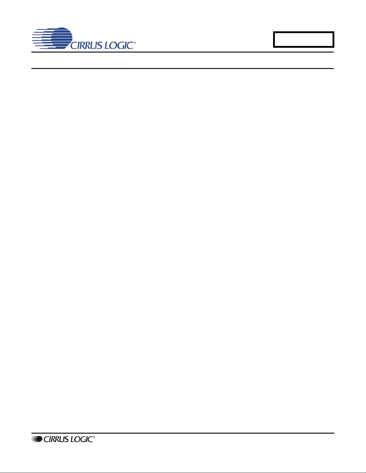
3. CORE CLOCK CIRCUITRY OF A CobraNet INTERFACE
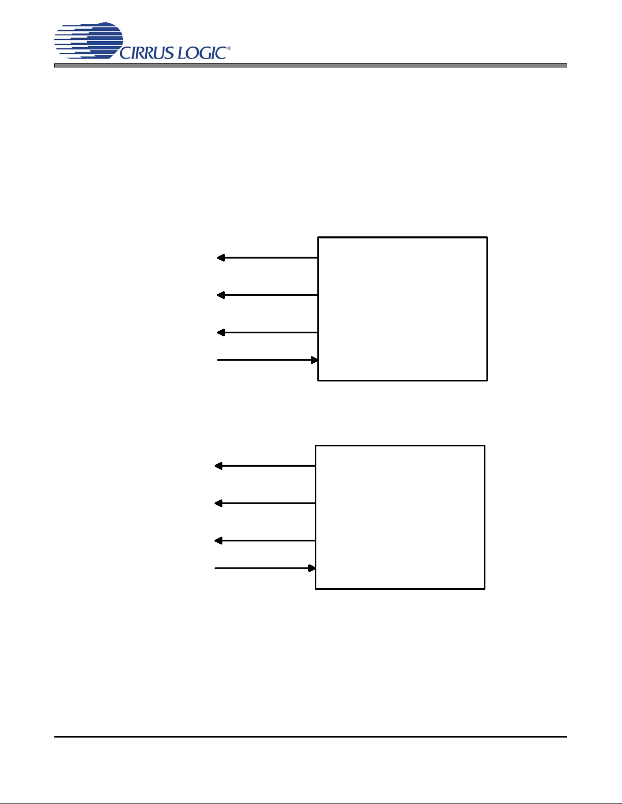
The core clock circuitry of a CobraNet interface is depicted in Figures 1 and 2. Note that not all inputs and outputs
to the clock module are used at the same time in all modes. Op eration of the circuitry, a nd activity on each path, are
dependent on the clock mode selected. These different clocking modes can be used in many ways, depending on
the requirements of a particular application. Common usage of the different modes is described in this document.
The user-available external clock connections are REFCLK, MCLK_IN, MCLK_OUT, FS1, and SCLK. The other
connections are internal to the interface and utilized by the interface's firmware in response to the particular mode
in use.
The five audio clock modes are:
• 0x00 - Internal (Normal Default Mode)
• 0x10 - Internal with External Sample Synchronization
• 0x01 - External Word Clock
• 0x04 - External Master Clock
• 0x14 - External Master Clock with External Sample Synchronization
Copyright © Cirrus Logic, Inc. 2008
http://www.cirrus.com
(All Rights Reserved)
MAY ‘08
AN312REV2
Page 2
MCLK_OUT (master)
AN312
DAC
MCLK_IN
MCLK_SEL
REFCLK_Enable
REFCLK_Polarity
REFCLK
Beat Received
Clock Config
Signal
Path
Control
Path
control
VCXO
24.576MHz
+/- 100 PPM
Clock
Out
MCLK
MUX
Edge
Detect
RST
Beat
MUX
Sample
Phase
Counter
Hardware FPGA Software
Figure 1. - CobraNet Clock Circuit for CM-1 Module
Audio
Clock
Generator
Phase
Detector
FS1 (word)
SCK (bit)
Loop
Filter
DAC
MCLK_IN
MCLK_S EL
REFCLK
Beat Received
Clock Config
Signal
Path
Control
Path
control
VCXO
24.576MHz
+/- 100 PPM
Clock
Out
MCLK
MUX
Beat
MUX
Sample
Phase
Counter
External
Hardware
Audio
Clock
Generator
CobraNet
Processor
Figure 2. CobraNet Clock Circuit for CM-2 Module and Semiconductors
Phase
Detector
MCLK _OU T (m aster)
FS1 (word)
SCK (bit)
Loop
Filter
Software
2 AN312REV2
Page 3
3.1 CobraNet Clock Modes
This section describes each of the CobraNet clock modes.
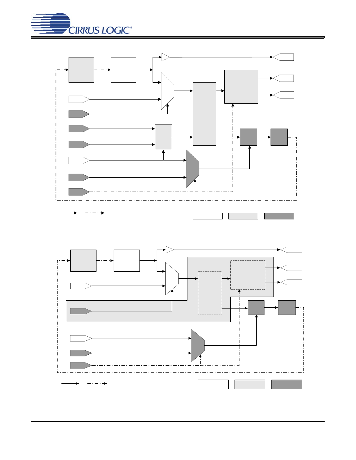
3.1.1 0x00 Mode - Internal Mode (Default)
The 0x00 Mode is the default clock mode of a CobraNet interface. When operating in this mode:
• As Conductor: The master audio clock (MCLK) is generated by the VXCO parked at its center frequency. Word clock (FS1) and bit clock (SCLK) are derived directly from MCLK.
• As Performer: The master audio clock (MCLK) is generated by the VXCO, which receives frequency
adjustments from the beat packets received from the Conductor node over the network interface, insuring that the Performer's clock is in sync with th e Conductor. Wo rd clock (FS1 ) and bit clock (SCLK)
are derived from MCLK.
MCLK_OUT
(Master Audio
(
DAC or ADC
Clock)
S
F
c
R
L
AN312
1
c
l
)
o
k
CobraNet Int erface
DAC
MCLK_IN
MCLK_SEL
REFCLK _Enable
REFCLK_Polarity
REFCLK
Beat Received
Clock Config
control
SCLK
(Bit clock)
Figure 3. 0x00 Mode Typical Connections
VCXO
24.576MHz
+/- 100 PPM
Clock
Out
MCLK
MUX
Edge
Detect
RST
Beat
MUX
Sample
Phase
Counter
Audio
Clock
Generator
Phase
Detector
MCLK_OUT (master)
FS1 (word)
SCK (bit)
Loop
Filter
Signal
Path
Control
Path
Active
Signal
Path
Hardwa re FPGA Software
Figure 4. Clock Circuit as Used by 0x00 Mode with CM-1 Module
AN312REV2 3
Page 4
DAC
MCLK_IN
MCLK_SEL
REFCLK
Beat Received
Clock Config
control
VCXO
24.576MHz
+/- 100 PPM
Clock
Out
MCLK
MUX
Beat
MUX
Sample
Phase
Counter
Audio
Clock
Generator
Detector
Phase
MCL K_O U T (m aster)
FS1 (word)
SCK (bit)
Loop
Filte r
AN312
Signal
Path
Control
Path
Active
Signal
Path
External
Hardware
CobraNet
Processor
Figure 5. Clock Circuit as Used by Mode 0x00 with CM-2 and Semiconductors
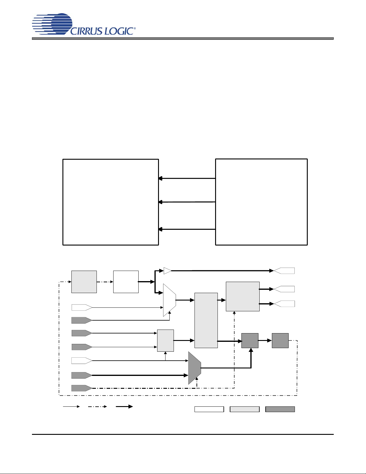
3.1.2 0x10 Mode - Internal Mode with External Sample Synchronization
Note: This will not work properly with CM-2 modules or semiconductor-based designs due to the absence of the edge detect circuit in the semiconductor.
This mode is similar to Internal Mode (0x00), but allows synchronization of the derived SCLK and FS1
signals with external clock circuits. It is typically used when it is necessary to sync hronize CobraNet clocks
with existing external clock circuitry. When operating in this mode:
• As Conductor: MCLK, FS1, and SCLK are all generated as in 0x00 Mode. Howeve r, the REFCLK input is used to align the clock edges of the generated MCLK, insuring that the audio clocks generated
externally are kept in sync with the CobraNet inte rface's audio clocks. This mode does not alter the
clock frequency and implies that the REFCLK input should be derived from the MCLK_OUT supplied
by the CobraNet interface (see Figure 6).
• As Performer: MCLK is generated by the VXCO, which receives frequency adjustments from the beat
packets received over the network interface as in 0x00 Mode. FS1 and SCLK are derived from MCLK.
As above in Conductor Mode, the REFCLK input is used to ensure that the external and CobraNet generated audio clocks are in sync.
Softw a re
SCLK
Clock Circuit
Clock In
FS1
24.576 MHz
MCLK_OUT
FS1
REFCLK
CobraNet Interface
Figure 6. 0x10 Mode Typical Connections (Sync of CobraNet Clocks with External Clock Circuitry)
4 AN312REV2
Page 5
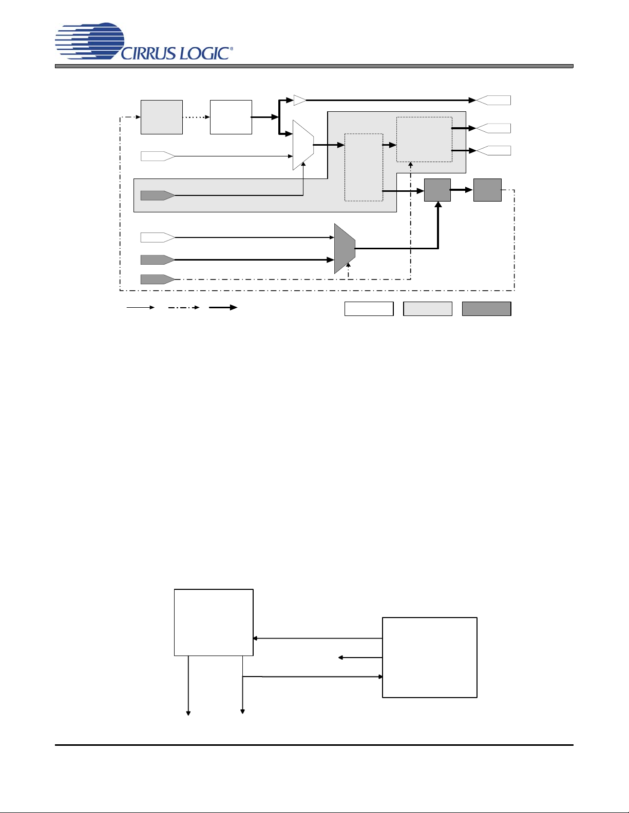
3.1.3 0x01 Mode - External Word Clock
External Word Clock Mode allows synchronization of all CobraNet clocks with an externally supplied word
clock. The external clock can be any integral division of FS1 from 750 Hz to 48 kHz. This is most often
used to synchronize a CobraNet network with a house sync signal whereby the Conductor will supply the
network clock and operate in this mode with Performer Nodes operating in 0x00 Mode. When operating
in this mode:
• As Conductor: The VCXO generating MCLK is steered to synchronize with REFCLK. FS1 and SCLK
are derived from MCLK.
• As Performer: The VCXO generating MCLK is steered to synchronize with REFCLK. FS1 and SCLK
are derived from MCLK.
FS1
SCLK
MCLK_OUT
AN312
CobraNet Interface
(External Word Clock Mode)
(conductor)
From house sync
Figure 7. 0x01 Mode Typical Connection (External Sync Attached to Conductor)
Note: Connection used to provide synchronized audio clocks via Ethernet
REFCLK
FS1
SCLK
CobraNet Interface
(External Word Clock Mode)
From house sync
Figure 8. 0x01 Mode Typical Connection - External Sync
MCLK_OUT
REFCLK
(conductor)
AN312REV2 5
Page 6

AN312
FS1
SCLK
CobraNet Interface
MCLK_OUT MCLK_OUT MCLK_OUT
(External Word Clock
Mode)
REFCLK
FS1
SCLK
FS1
SCLK
CobraNet Interface
(External Word Clock
Mode)
REFCLK
Figure 9. 0x01 Mode Typical Connection - Synchronization of All Nodes
Note: All nodes should be on house synch.
Clock
Out
MCLK
MUX
Audio
Clock
Generator
DAC
MCLK_IN
control
VCXO
24.576MHz
+/- 100 PPM
CobraNet Interface
(External Word Clock
Mode)
REFCLK
48 kHz House Sync
MCLK_OUT (master)
FS1 (word)
SCK (bit)
MCLK_SEL
REFCLK_Enable
REFCLK_Polarity
REFCLK
Beat Received
Clock Config
Signal
Path
Sample
Phase
Counter
RST
Beat
MUX
Hardware FPGA Software
Control
Path
Active
Signal
Path
Edge
Detect
Figure 10. Mode 0x01 Clock Circuit Used with CM-1 Modules
Phase
Detector
Loop
Filter
6 AN312REV2
Page 7

DAC
MCLK_IN
MCLK _SEL
REFCLK
Beat Received
Clock Config
control
VCXO
24.576MHz
+/- 100 PPM
Clock
Out
MCLK
MUX
Beat
MUX
Sample
Phase
Counter
Audio
Clock
Generator
Phase
Detector
AN312
MCLK _OU T (m aster)
FS1 (word)
SCK (bit)
Loop
Filter
Signal
Path
Control
Path
Active
Signal
Figure 11. Clock Circuit as Used by Mode 0x01 with CM-2 and Semiconductors
3.1.4 0x04 Mode - External Master Clock
In External Master Clock Mode, all clocks are derived from an externally supplied master clock of
24.576 MHz. This mode is provided because it is easy to accomplish using the existing clock circuitry. It
is most useful when trying to synchronize one or more CobraNet devices to a distributed Master Clock.
However, it has little practical utility because it is difficult to properly distribute a clock of this frequency
and does not provide a means to ensure synchronization of the audio clocks (SCLK, FS1). Note that
MCLK_OUT is not a copy of MCLK_IN. MCLK_OUT is derived from the VCXO, which is not controlled in
this mode and is not synchronous with the supplied MCLK_IN. When operating in this mode:
• As Conductor: MCLK is sourced directly from MCLK_IN. FS1 an d SCLK are derived from MCLK_IN.
• As Performer: MCLK is sourced directly from MCLK_IN. FS1 and SCLK are derived from MCLK_IN.
FS1
(LR clo ck)
SCLK
(Bit clock)
External
Hardware
CobraNet Interface
CobraNet
Processor
So ftw a r e
MCLK_IN24.576 MHz
Figure 12. 0x04 Mode Typical Connection (Synchronization to an Externally-Supplied Master Clock)
AN312REV2 7
Page 8

DAC
MCLK_IN
control
VCXO
24.576MHz
+/- 100 PPM
Clock
Out
MCLK
MUX
Audio
Clock
Generator
AN312
MCLK_OUT (m aster)
FS1 (word)
SCK (bit)
REFCLK _En able
REFCLK_Polarity
Signal
Path
DAC
MCLK_IN
MC LK_SE L
MCLK_SEL
REFCLK
Beat Received
Clock Config
Control
Path
Active
Signal
Path
Edge
Detect
Sample
Phase
Counter
RST
Beat
MUX
Hardwa re FPGA Softw a re
Figure 13. Clock Circuit as Used by Mode 0x04 with CM-1 Module
control
VCXO
24.576MH z
+/- 100 PPM
Clock
Out
MCLK
MUX
Sample
Phase
Counter
Phase
Detector
Audio
Clock
Generator
Phase
Detector
Loop
Filter
MC LK_ O UT (m aster)
FS1 (word)
SCK (bit)
Loop
Filter
REFCLK
Beat
Beat Received
Clock Config
Signal
Path
Control
Path
Active
Signal
Path
MUX
External
Hardware
CobraNet
Processor
So ftw a re
Figure 14. Clock Circuit as Used by Mode 0x04 with CM-2 and Semiconductors
8 AN312REV2
Page 9

AN312
3.1.5 0x14 Mode - External Master Clock with External Sample Clock Synchronization
Note: This mode operates differently depending on use of the CM-1 or CM-2 CS1810xx/CS4961xx
chip-based products.
3.1.5.1 0x14 Mode for CM-1
In this mode, all clocks are derived from an externally supplied master clock of 24.576 MHz. This mode
is provided primarily to allow synchronization of multiple CobraNet interf aces within the same cha ssis. It
can also be used, as in 0x10 Mode, to synchronize external clock circuitry derived from an external master
clock. Note that MCLK_OUT is generated by the VCXO in this mode and is not a copy of MCLK_IN. When
operating in this mode:
• As Conductor: MCLK is supplied by the MCLK_IN input. FS1 and SCLK are der ive d fro m MCLK_IN.
As in 0x10 Mode, REFCLK is used to synchronize the clocks.
• As Performer: MCLK is supplied by the MCLK_IN input. FS1 and SCLK are derived from MCLK_IN.
As in 0x10 Mode, REFCLK is used to synchronize the clocks.
FS1
(LR clock)
SCLK
(Bit clock)
CobraNet Interface
24.576 MHz
LR Clock
Figure 15. 0x14 Mode Typical Connection
(Synchronization to an Externally-Supplied Master Clock and Word Clock when Using CM-1)
MCLK_IN
REFCLK
AN312REV2 9
Page 10

FS1
(LR clock)
SCLK
(Bit clock)
CobraNet
Interface
(Master)
Typically Mode
0x00
AN312
MCLK_OUT
24.576 MHz
FS1
FS1
(LR clock)
SCLK
(Bit clock)
CobraNet Interface
(Slave)
Mode 0x14
MCLK_IN
REFCLK
FS1
(LR clock)
SCLK
(Bit clock)
CobraNet Interface
(Slave)
Mode 0x14
MCLK_IN
REFCLK
Figure 16. 0x14 Mode Typical Connection
(Master and Reference Clock Supplied to Slave Interfaces within Same Chassis when Using CM-1)
MCLK_O U T (m aster)
DAC
MCLK_IN
MCLK_SE L
REFCLK_E nable
REFCLK_ Polarity
control
VCXO
24.576MHz
+/- 100 PPM
Clock
Out
MCLK
MUX
Edge
Detect
RST
Sample
Phase
Counter
Audio
Clock
Generator
Phase
Detector
FS1 (word)
SCK (bit)
Loop
Filter
REFCLK
Beat
Beat Received
Clock Config
Signal
Path
Control
Path
Active
Signal
Path
MUX
Hardware FP GA Software
Figure 17. Clock Circuit as Used by Mode 0x14 with CM-1 Module
10 AN312REV2
Page 11

3.1.6 0x14 Mode for CM-2/CS1810xx/CS4961xx-Based Devices
Note: The 0x14 clock mode only works with devices running Rev. 2.11.6 firmware or later.
Mode 0x14 for CM-2 and CobraNet chips is primarily intended to allow complete audio clock slaving of
one or more CobraNet devices to a master CobraNet device within the same chassis.
MCLK, SCLK, and FS1 are all supplied to the slave device by the master device. External divide by 2 logic
must also be used on DAI1_SCLK when using 16x16 channel chips.
Changing to this mode dynamically has not proven to work well consistently. The CNCustom firmware
modification program should be used to create slave device firmware with the Conductor and Performer
clock modes set to values of 0x14 so that the slave device(s) will boot up in mode 0x14. The hardware
should be designed so that the slave device(s) will always be supplied by all required clocks and will always operate in mode 0x14. The internal clock circuitry for the master device will be as that shown and
described elsewhere in this document for the master clock mode in use. A description o f the internal clock
circuitry is not applicable for the slave device(s) as all clocks are supplied to them directly.
AN312
VCXO
MCLK_IN (8)
DAO1_SCLK (20)
DAI1_SCLK (137)
DAO1_LRCLK (22)
DAI1_LRCLK (138)
CobraNet Interface
(Master)
(Typically Mode 0)
24.576 MHz
MCLK_IN (8)
3.072 / 6.144 MHz
DAO1_SCLK (20)
DAI1_SCLK (137)
48 / 96 kHz
DAO1_LRCLK (22)
DAI1_LRCLK (138)
CobraNet Interface
(Slave)
Mode 0x14
Figure 18. Clock Circuit as Used by Mode 0x14 with CM-2 or Chips with 2x2 or 8x8 Audio Channels
2
.
4
5
7
6
M
z
VCXO
MCLK_IN (8)
DAO1_SCLK (20)
DAI1_SCLK (137)
DAO1_LRCLK (22)
DAI1_LRCLK (138)
6.144 MHz
/2
.
3
0
96 kHz
48 kHz DAO2_LRCLK (14)DAO2_LRCLK (14)
H
2
7
M
MCLK_IN (8)
DAO1_SCLK (20)
DAI1_SCLK (137)
H
z
DAO2_SCLK (12)
DAO1_LRCLK (22)
DAI1_LRCLK (138)
CobraNet Interface
(Master)
(Typically Mode 0)
CobraNet Interface
(Slave)
Mode 0x14
Figure 19. Clock Circuit as Used by Mode 0x14 with CM-2 or Chips with 16x16 Audio Channels
AN312REV2 11
Page 12

AN312
4. USING 0x10 MODE WITH CS1810XX, CS4961XX OR CM-2
0x10 Mode is used when the designer wishes to synchronize the CobraNet clocks with an externally supplied word
clock (FS1). This is not possible with CM-2 and Silicon-based designs. The best that can be achieved is to use the
circuitry below to ensure that the audio clocks of the CobraNet interface are in phas e with the audio clocks of the
existing circuit. In this case, the master clock is derived from the CobraNet device by using the circuitry shown in
Figure 20, with the interface set to operate in clock mode 0x00. Any clocks required by the design can be taken from
the loadable counter taps, and these clocks will be in phase with the audio clocks (FS1 and SCLK) generated by the
CobraNet device. The Data In load value can be adjusted to ensure phase alignment if necessary.
Load
AND
Q
D Flop
D
QD
D Flop
FS1
SCLK
Loadable Counter
Clock In
Data In
FS1
= 0x002
Clock In
24.576 MHz
Figure 20. 0x10 Mode Circuitry for Use with CM-2, CS1810xx or CS4961xx
5. REFERENCES
1. CobraNet Programmer's Reference Manual, http://www.cirrus.com
2. CobraNet Hardware User's Manual, http://www.cirrus.com
Clock In
CobraNet Interface
MCLK_OUT
12 AN312REV2
Page 13

6. REVISION HISTORY
Release Changes
Revision 1 Initial Release.
Revision 2 Added more detail to Figures 18 and 19. Clarified langua ge in Section 3.1.6 on page 11.
AN312
AN312REV2 13
Page 14

AN312
Contacting Cirrus Logic Support
For all product questions and inquiries, contact a Cirrus Logic Sales Representative.
To find the one nearest you, go to www.cirrus.com.
IMPORTANT NOTICE
Cirrus Logic, Inc. and its subsidiaries (“Cirrus”) believe that the information contained in this document is accurate and reliable. However, the information is subject
to change without noti ce and is p rovided “AS IS” wit hout warran ty of any k ind (expr ess or i mplied). Customers are advis ed to ob tain the latest version of relevant
information to verify, before placing orders, that information being relied on is current and complete. All products are sold subject to the terms and conditions of sale
supplied at the time of order acknowledgment, including those pertaining to warranty, indemnification, and limitation of liability. No responsibility is assumed by Cirrus
for the use of this information, including use of this information as the basis for manufacture or sale of any items, or for infringement of patents or other rights of thir d
parties. This document is the property of Cirrus and by furnishing this information, Cirrus grants no license, express or implied under any patents, mask work rights,
copyrights, trademarks, trade secrets or other inte llectual property rig hts. Cirrus owns the copyrights associated with the information contained herein and gives consent for copies to be made of the information only for use within your organization with respect to Cirrus integrated circuits or other products of Cirrus. This consent
does not extend to other copying such as copying for general distribution, advertising or promotional purposes, or for creating any work for resale.
CERTAIN APPLICATIONS USING SEMICONDUCTOR PRODUCTS MAY INVOLVE POTENTIAL RISKS OF DEATH, PERSONAL INJURY, OR SEVERE PROPERTY OR ENVIRONMENTAL DAMAGE (“CRITICAL APPLICATIONS”). CIRRUS PRODUCTS ARE NOT DESIGNED, AUTHORIZED OR WARR ANTED FOR USE
IN PRODUCTS SURGICALLY IMPLANTED INTO THE BODY, AUTOMOTIVE SAFETY OR SECURITY DEVICES, LIFE SUPPORT PRODUCTS OR OTHER CRITICAL APPLICATIONS. INCLUSION OF CIRRUS PRODUCTS IN SUCH APPLICATIONS IS UNDERSTOOD TO BE FULLY AT THE CUSTOM ER’S RISK AND CIRRUS DISCLAIMS AND MAKES NO WARRANTY, EXPRESS, STATUTORY OR IMPLIED, INCLUDING THE IMPLIED WARRANTIES OF MER CHANTABILITY AND
FITNESS FOR PARTICULAR PURPOSE, WITH REGARD TO ANY CIRRUS PRODUCT THAT IS USED IN SUCH A MANNER. IF THE CUSTOMER OR CUSTOMER’S CUSTOMER USES OR PERMITS THE USE OF CIRRUS PRODUCTS IN CRITICAL APPLICATIONS, CUSTOMER AGREES, BY SUCH USE, TO FULLY
INDEMNIFY CIRRUS, ITS OFFICERS, DIRECTORS, EMPLOYEES, DISTRIBUTORS AND OT HER AGE NTS FRO M ANY AND AL L LI ABI L IT Y, I NCL UDING ATTORNEYS’ FEES AND COSTS, THAT MAY RESULT FROM OR ARISE IN CONNECTION WITH THESE USES.
Cirrus Logic, Cirrus, th e Ci rru s Log ic logo d esi gns a nd Cobra Net are tr ademar ks of Cirr us Lo gic , I nc. All ot her br and and prod uct names in this document may be
trademarks or service marks of their respective owners.
14 AN312REV2
 Loading...