

Page 1

AN31
Application Note
A Collection of Brid ge Transducer Digitizer Cir cuits
by
Jerome Johnston
Introduction
Bridge transducers are common in
instrumentation. This application note illustrates
some bridge transducer digitizer circuits which
use the CS5504/5/6/ 7/8/9 A/D converters and the
CS5516/20 A/D co nverters.
The CS5504/5/6/7/8 converters can be operated
with a variety of power supply arrangements;
including operating from a single +5 V supply;
operating from +5 and -5 analog supplies with
+3.3 V or +5 V on the digital supply; or
operating with an analog supply from +5 to
+11 V and a digi tal supply of +5 V.
The CS5509 can oper ate with +5 V on its analog
and digital supplies; or with +5 V analog and
+3.3 V digita l.
The CS5516 and CS5520 are A/D converters
optimized for bridge transducer applications and
are designed to operate from +5 and -5 V
supplies. Several circuits which utilize these
ADCs will be presented.
The applicatio n note is divi ded into two sections:
1. DC-excited bridge circuits.
2. AC-excited bridge circuits with a discu ssion
of the benefits of AC excitation.
Bridge Tran sducers
Bridge transducers are manufactured with
various technologies. The strain-sensing
elements which make up the bridge may be
made of diffused silicon, bonded silicon bars,
deposited thin film, or bonded foil materials.
The choice of technology will determine the
performance of the transducer, including the
sensitivity, the linearity, and the thermal
stability. Si licon-based gages hav e good linearity
with sensitivities between 3 mV/V and
20 mV/V, but tend to exhibit more drift as
temperature changes. Metal foil or thin film
gages have good linearity with sensitivities
between 1 mV/V and 4 mV/V. Precision bridge
transducers include some type of temperature
compensation as part of the bridge .
Most bridge circuits are excited with a dc
voltage, 10 v olts bei ng very common . With 10 V
excitation, the full scale signa ls from the various
transducers, can be as low as 10 mV to as high
as several hundred millivolts. When digitizing
these signals to high resolution (for discussion in
this application note, high resolution means
greater than 10,000 counts), one count can
represent a very small voltag e. It can be diffi cult
to amplify and digitize these low level bridge
transducer signals. Measurement performance
can be hindered by such things as amplifier
Crystal Semiconductor Corporation
P.O. Box 17847, Austin, TX 78760
(512) 445-7222 FAX 445-7581
http://www.crysta l.com
Copyright Crystal Semiconductor Corporation 1996
(All Rights Reserved)
JAN ’95
AN31REV3
1
Page 2
Bridge Transducer Digitizer Circuits
offset drift, amplifier noise (both thermal and
1/f), amplifier finite open loop gain, and
parasitic thermocouples. Parasitic thermocouples
are introduced any time two dissimilar metals
are connected. For example, using tin-lead solder
to solder a wire to a copper PC trace can
introduce an unwanted thermocouple junction
which changes as much as 3 µV/°C when
subjected t o temperat ure gradient s.
This application note will introduce some A/D
converter circuits which illustrate a number of
application ideas to the design engineer who
uses bridge transducers. In the AC-excited
bridge section, a number of design ideas will b e
introduced which offer very good solutions to
some of the problems encountered in low level
bridge measurement.
+5
5.23k
350350
100 pF
-
5k
350 350
40.2k
1k
Optional
Zero
Trim
5k
3 mV/V
Transducer
+
LTC1051
0.1
3
2
6
5
1
0.47
0.47
7
4
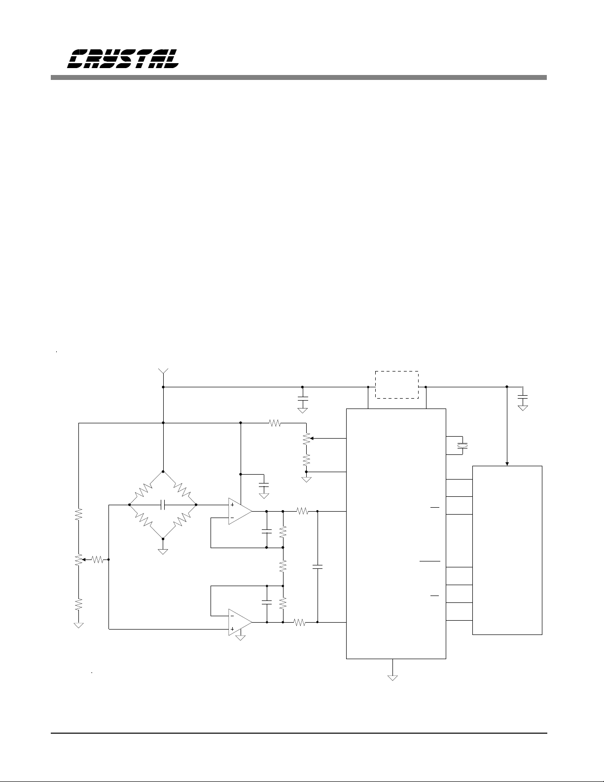
DC-EXCITED BRIDGE CIRCUITS
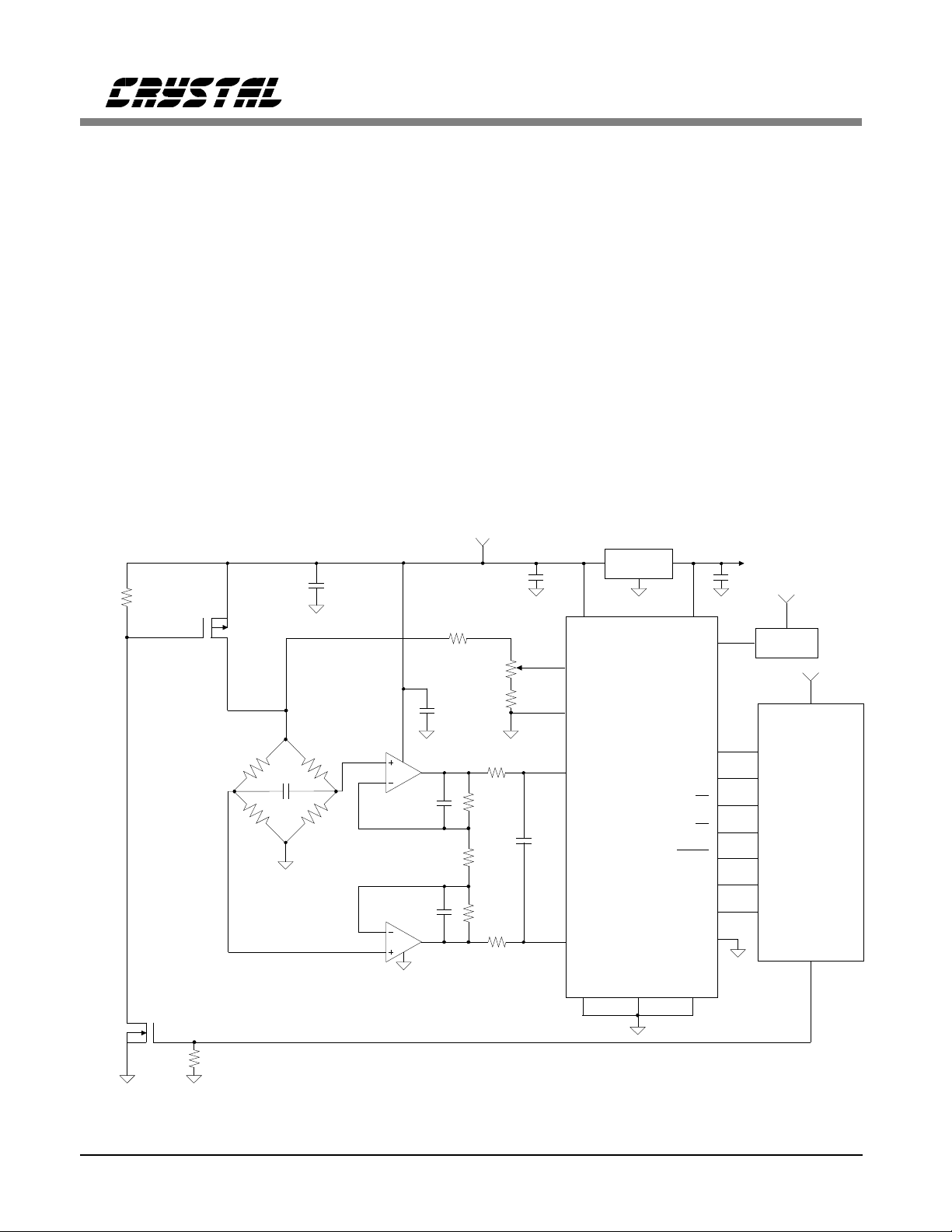
CS5507,8,9 Bridg e Transducer Operating
From a Single +5 V Supply, or with the
Analog Supply at +5 V and Digital Supply at
+3.3 V
Figure 1 illustrates the low cost CS5509 16-bit
converter operating from +5 V. The A/D can
operate in either unipolar or bipolar mode and
yields 20 c onversions/second wh en running from
a low cost 32.76 8 kHz crystal. When operated at
32.768 kHz the digital filter in the converter
notches out 50 and 6 0 Hz line interfere nce.
The LTC1051 dual chopper amplifier is used as
the bridge amplifier. Bandwidth is limited to
about 3.8 Hz b y the 100k and 0.47 µF feedback
+3.3 V
500
10k
100k
931
100k
100
100
0.1
Optional
Gain
Trim
≈
3.25 V
0.1
VA+ VD+
9
VREF+
10
VREF-
7
AIN+
8
AIN-
Regulator
11 13
XIN
XOUT
CAL
CONV
CS
CS5509
16 bits
DRDY
SDATA
BP/UP
SCLK
+5V or +3.3V
4
5
3
2
1
16
15
6
14
VD+ can be
32.768kHz
Microcontroller
0.1
System
20 Conversions/sec.
GND
12
Figure 1. CS5507,8,9 Bridge Transducer Operating from a Single +5 V Supply, or with the Analog Supply at +5 V
and Digital Supply at +3.3 V.
2 AN31REV3
Page 3
Bridge Transducer Digitizer Circuits
elements of the amplifier stage. Note that an
instrumentation amplifier is not needed because
the A/D input is fully differential. The dual
amplifier functions as a differential in,
differential out amplifier. The circuit yields
about 9000 noise-free counts when measuring
unipolar s ignals. Averag ing 10 sample s increases
this to about 28,500 noise-free counts.
"Noise-free counts" means full scale signal
divided by six times the rms noise. Noise-free
counts is good figure of merit for comparing
A/D converters used in dc measurement
applications. There is more discussion on this
topic at the e nd of the app lication no te.
The circuit illustrated uses a 3 mV/V transducer
excited with +5 V for a full scale transducer
output of 15 mV. The transducer output is
amplified with a gain of about 216 to yield
3.25 V full scale. A dual stage amplifier, as
shown in Figure 2 may be preferred to minimiz e
errors due to limited loop gain. The A/D is
operated in bipolar mode to achieve more
µV/LSB. The reference voltage for the converter
is derived from th e +5 V excitation voltage. The
measurement remains ratiometric should the
+5 V excitatio n change.
Figure 1 includes potentiometers for offset and
gain adjustment , as do a numbe r of other circuits
in this application note. Many system designers
prefer to eliminate potentiometers and do all
offset and gain correction in software. To
+5
10k
1k
10k
x216
4.32k
20k
20k
Figure 2. Dual Stage Amplifier
achieve this in some of the circuits may require
changes to gain stages or voltage references , but
potentiometers are shown for all the engineers
who are more comfortable with screwdrivers
than software.
The CS5509 in Figure 1 can run as fast as 200
conversions per second if operated with a
330kHz external clock. Figure 3 shows an RC
gate oscillator which can produce stable
frequencies, or a CMOS 555 timer can be used.
The gate oscillator ca n be operated from either a
+5 or +3.3 V supply and maintains fairly good
frequency sta bility ove r temperatur e.
+3.3 to +5
10
R
R
1
74HC04
2
0.1
f
162kHz
200kHz
output
330kHz
C
f ≈
2 (R + R ) C
R
1
10k
8.2k
5k
1.44
1 2
R
3.4k
2.7k
1.6k
2
R
2 1
330pF
330pF
330pF
≈
R
3
C
Figure 3. Temp erature -Stabl e Gate Oscill ator fo r +5 or +3 .3 Vol ts.
AN31REV3 3
Page 4
Bridge Transducer Digitizer Circuits
All of the converters (CS5504-09) can be
operated with a single +5 V supply. All of the
converters can also be operated with +5 V
analog supply and +3.3 V on the digital supply.
If this dual supply arrangement is used, the
digital supply should be derived from the analog
supply to ensure proper operation. Under all
conditions, including start-up, th e voltage on the
VA+ pin must be the more positive than any
other pin on the device to ensure proper
substrate bias ing of the c hip.
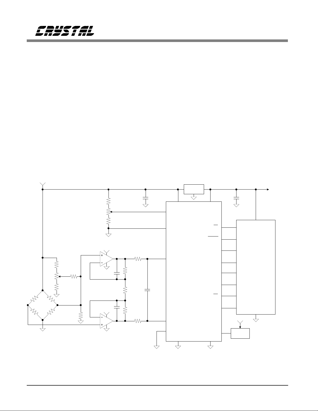
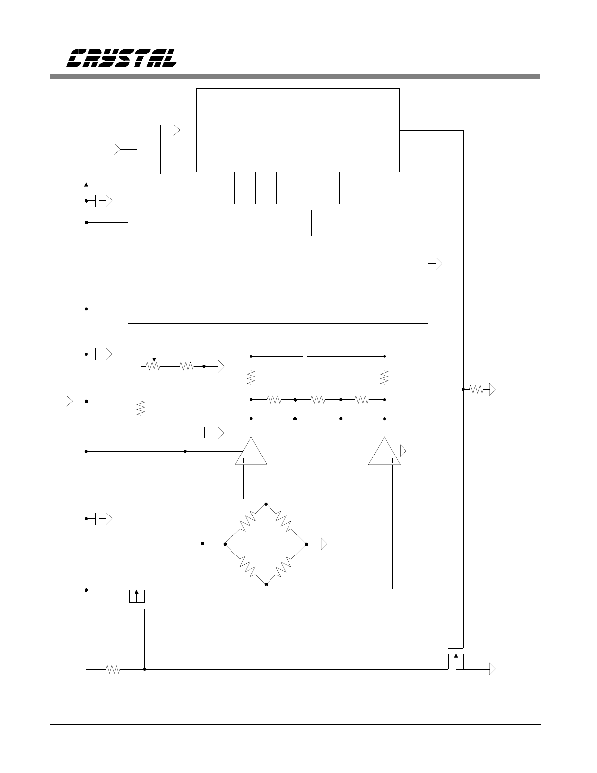
CS5507/8 with +10 V Analog Suppl y and
+5 V Digital Supply
It is common for many weigh scales to be
operated from batteries with a 12 V
+10
Optional
-
350 Ω Bridge
2mV/V
5k
3.57k
1k
Optional
Fine
Offset
Adjust
+
Resistor
200k
Coarse
200k
Offset
100 Conversions/sec
20k
1k
10k
x332
+10
LT1007
0.047
0.047
+10
LT1007
Gain
Trim
100
75k
453
75k
100
automotive-type battery being common. The
CS5504/5/6/7/8 devices can be operated with
higher supply voltage on the analog portion of
the chip than on the digital portion (Note: the
CS5509 is an e xception and is specified with an
analog supply of +5 V onl y). The analog supply
(VA+) must always be the most positive voltage
on the chip to ensure proper operation. Figure 4
illustrates the CS5507 operating from +10 V on
the analog an d +5 V on the digit al. The bridge is
excited wit h the +10 V and resistors are used to
divide this excitation supply to obtain a
ratiometric vol tage reference of abou t 3.33 V for
the converter. The circuit is designed to operate
with the A/D in bipolar mode to yield more
µV/count. Th e A/D is set-up for an inpu t span of
± 3.33 V. A 200k pull down resistor forces a
+5Volt
Regulator
0.33
≈
3.33 V
0.047
14
VA+ VD+
VREF+
11
VREF-
12
8
AIN+
CS5507
CS5508
16 or
20 bits
10
AIN-
13
VREFOUT
VA- DGND
15
+5
17
CS
DRDY
SCLK
SDATA
CONV
M/SLP
BP/UP
CAL
XIN
16
1
20
18
19
2
6
7
3
4
0.1
+5
System
Microcontroller
+5
162kHz
+5
Figure 4. CS5507/8 with +10V Analog Supply and +5 V Digital Supply.
4 AN31REV3
Page 5
Bridge Transducer Digitizer Circuits
negative offset into the amplifier and the zero
trim is used to finely ad just this offset . With zero
weight on the scale, the zero trim is adjusted to
yield -30,000 co unts if the CS5507 1 6-bit A/D is
used or to -500,000 counts if a 20-bit CS5508 is
used. With full scale we ight on the scale the gai n
trim is adjusted for +30,000 counts in the
CS5507 or +500,000 counts in the CS5508
(Note that the CS5507 and CS5508 are pin
compatible). This leaves some counts for both
zero underflow and for overrange . The amplifier
components set the bandwidth to 45 Hz. With
the 45 Hz bandwidth, the circuit exhibits about
50,000 noise-free counts. With an external 162
kHz clock, the converter can operate at 100
+5
+5
7.5k
5k
-
0.47
2 mV/V
350 350
-5
20 Conversions/sec
7.5k
350350
+
2mV/V
Transducer
x100
3
2
INA131
+5
7
6
4
-5
Bridge Amp
#2
#3
#4
0.1
2.4k
0.1
conversions per second. If 20 conversion words
from the CS5508 are averaged, the circuit will
yield more than 200,000 noise-free counts. A
limitation of this circuit is that the bipolar
amplifiers can exhibit significant offset drift as
the temperature changes. There are several
circuits in this application note which will show
how to overcome offset drift.
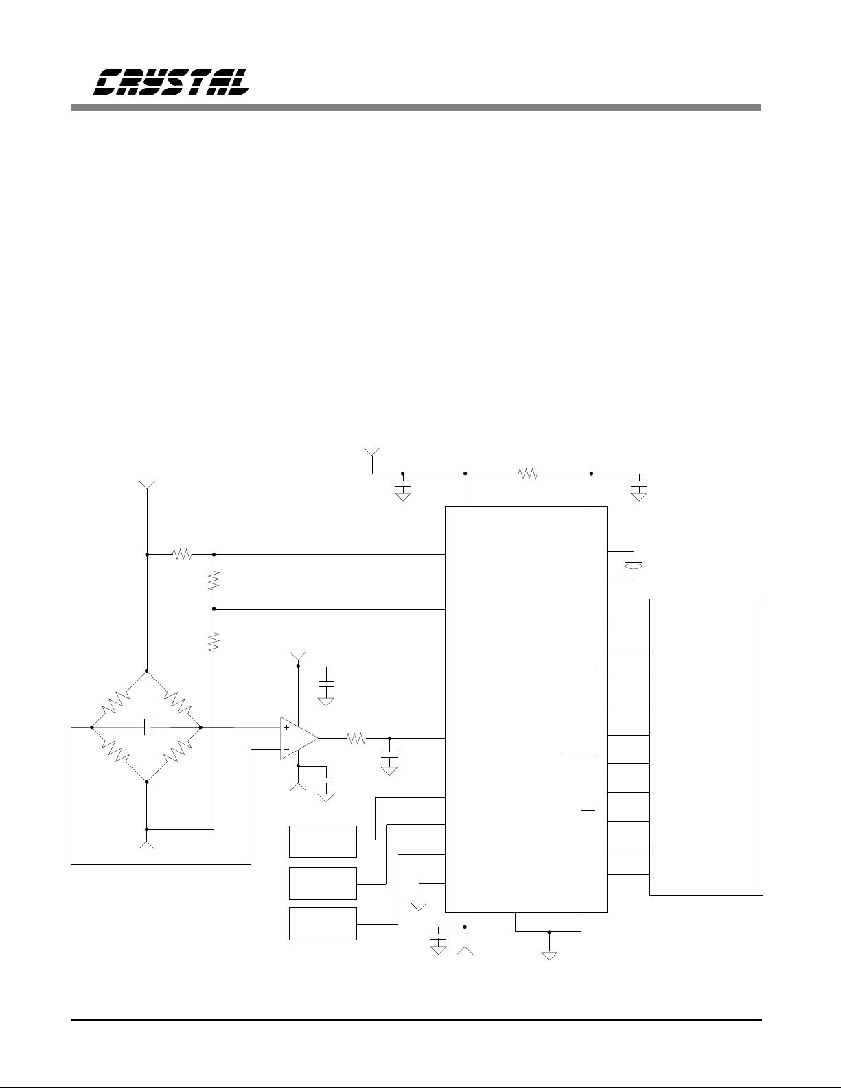
CS5505/6 Operating Fro m ± 5 V Supplies
The CS5504/5/6 /7/8 converte rs (not the CS550 9)
can be operated wit h ±5 V on the analog sectio n
of the converter, and with either + 5 V or +3.3 V
on the digita l section.
10
VD+
XIN
CS
A0
A1
0.1
20
5
32.768kHz
6
4
3
2
1
24
23
22
8
21
7
1916
System
Microcontroller
≈
0.1
0.1
2.5 V
10
0.1
14
15
12
13
11
9
17
VA+
VREF+
VREF-
CS5505
CS5506
AIN1+
AIN2+
AIN3+
AIN4+
AIN-
-5
20 bits
VREFOUTVA- DGND
18
XOUT
CAL
CONV
16 or
DRDY
SDATA
BP/UP
SCLK
M/SLP
Figure 5. CS5505/6 Operating from ± 5V Supplies.
AN31REV3 5
Page 6
Bridge Transducer Digitizer Circuits
Figure 5 illustrates an ap plication which uses an
instrumentation a mplifier to ampli fy and convert
the differential bridge signal to a
ground-referenced signal for the converter. Full
scale for the converter is set by the divider
resistors which determine the voltage reference
input to the VR EF+/- pins of the converter. The
reference voltage in the figure is set to 2.5 V.
The bridge sensitivity is 2 mV/V so the full
+
100k
TP0610L
Q2
10
0.1
scale bridge output is 20 mV. This is amplified
by the 100 gain of the instrumentation amplifier
to obtain 2 .0 V into the conv erter. The converter
can be operated in either unipolar or bipolar
mode. Up to four load cells, each with its own
amplifier, can be input to the CS5506. The
measurement assumes the voltage reference will
remain ratiom etric acros s all four l oad cells .
CS5507 Switched -Bridge Lo w-power
Digitizer with +10 V Excitation
Some applications call for reduced operating
power. One method of significantly redu cing the
power consumption is to apply the supply
voltage to the bridge transducer only when a
+10
10k
500
14
VA+
VREF+
VREF-
+5V Regulator
17
VD+
XIN
0.1
Optional
Gain
11
Trim
3.33 V
≈
5k
12
+5
0.1
4
162 kHz
+5
OSC
+5
3
CAL
CONV
BP/UP
DRDY
SDATA
SCLK
M/SLP
CS
1613
2
1
7
20
19
18
6
System
Microcontroller
2N7000
Q1, Q2 Siliconix
Q1
100k
350350
100pF
-
350
350
2 mV/V
Transducer
3
8
+
2
0.015
LT1013
0.015
6
5
1 Conversion = 20 msec
226
18.7k
x166
18.7k
100
100
0.047
8
AIN+
CS5507
16 bits
10
AIN-
VREFOUTVA- DGND
15
1
7
4
Figure 6. CS5 507 S witched- Bridg e Low -power Dig itizer wit h +10 Volt Excita tion .
6 AN31REV3
Page 7

Bridge Transducer Digitizer Circuits
measurement is required. Figure 6 illustrates an
example circuit in which the power to the bridg e
transducer is switched on only when a
measurement is desired.
The circuit as shown is optimized for a +10 V
analog supply. The circuit can be modified
(optimized) to operate from any analog supply
from 11 V to 6.5 V (assuming the +5 V
regulator needs 1.5 V of input/output
differential) by changing the resistor values
which determine the voltage reference to the
converter and by changing the gain resistors in
the amplifier to compensate for the cha nge in the
bridge output signal. The circuit shown
illustrates a 2 mV/V transducer outputting
20 mV full-scale. A g ain of 166 ampl ifies this to
3.32 V into th e A/D. The full-scale of the A/D is
set at 3.33 V by dividing down the excitation
voltage.
In the power arrangement shown, the CS5507
A/D uses about 4 mW. The con verter is clocked
from an external gate oscillator clock (162 kHz)
to yield a conversion time of 10 msec. When
power is applied to the bridge, a delay must
occur to allow the signal to settle before a valid
conversion can be pe rformed. Settling time to 16
bits after power is applied to the bridge takes
about 3.3 msec. The microcontroller can use an
internal ti mer to time about 4 msec. to allow for
the delay or the microcontroller can perform a
dummy conversion in the converter to allow for
settling time. When the dummy conversion is
finished (10 msec. later) the conversion data is
discarded and a second conversion is then
performed to make a valid measurement. After
the second conversion is complete (
DRDY falls
the second time) power to the bridge is
deactivated and the conversion word is clocked
out of the conv erter’s serial port.
Power consumed by the transducer dominates
the power dissipated in the circuit. Average
power consumption in the bridge c an be reduced
by a factor o f at leas t fifty (<6 mW) if the b ridge
is powered for only 20 msec. for a reading each
second. If even lower off power is desired, the
supply to the LT1013 ca n also be swit ched along
with the bridge excitation.
CS5509 Switched -Bridge Lo w-power
Digitizer with +5 V Excitation
The circuit in Figure 7 is similar to t he previous
one, but op erates from a sing le +5 V. The ci rcuit
shows a load cell with 3 mV/V sensitivity. A
2 mV/V transduce r can be use d if additional gain
is added; or the voltage reference into the
converter can be lowered to 1.67 V with some
minor increase in noise. Average power
consumption in the load cel l is only 1.5 mW for
one reading per se cond.
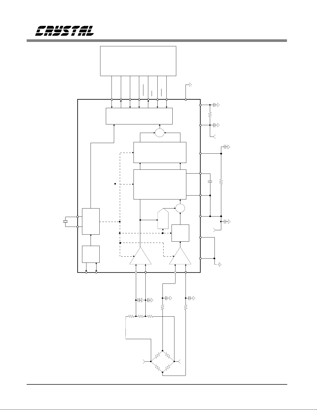
CS5516/CS5520 Using DC B ridge Excitation
The CS5516 (16-bit) and CS5520 (20-bit) A/D
converters are designed for bridge measurement
applications. They include an instrumentation
amplifier with X25 gain, a PGA (programmable
gain amplifier) with gains of 1, 2, 4, and 8, and
a four bit DAC which can trim out offset up to
± 200% of the full scale signal magnitude. The
input span can be adjusted by changing either
the magnitude of the voltage at the VREF pins
of the converter or by changing t he PGA gain.
In the circuit shown in Figure 8, the bridge is
excited with ± 5 v olts. Resis tors R1, R2 , and R3
divide the excitation voltage to give a 2.5 V
reference signal into the VREF pins. The input
span at the AIN pins of the converter is
determined by dividing the voltage at the VREF
pins by the PGA gain and the X25
instrumentation amplifier gain. For example,
with 2.5 V into the VREF pins, and the PGA set
to a gain o f 8, the input span at the AIN pins is
2.5/(8 X 25) = 12.5 mV in unipolar mode or
± 12.5 mV in bipolar mode. Th e converter offers
several calibration features to remove offset and
to calibrate the gain slope. The input span of
AN31REV3 7
Page 8
Bridge Transducer Digitizer Circuits
+5
+5
+5
+5
0.1
13
11
0.1
10k
VD+
VA+
OSC
162 kHz
3
4
XIN
VREF+
9
Gain
Optional
500
VREF-
10
Trim
10k
0.1
2
CAL
CONV
AIN+
7
100
1
8
System
Microcontroller
1
6
16
15
14
CS
18.7k
0.015
DRDY
BP/UP
CS5509
16 bits
0.047
X 166
226
SCLK
SDATA
12
GND
AIN-
8
18.7k
0.015
100
7
4
100k
3
2
10
+
+
350350
100 pF
LT1013
350
3 mV/V
6
5
1 Conversion = 20 msec
Figure 7. CS5 509 S witched- Bridg e Low -power Dig itizer wit h +5 V olt E xcit atio n.
-
Q2
TP0610L
100k
350
Q1, Q2 Siliconix
Q1
2N7000
8 AN31REV3
Page 9
POST
Bridge Transducer Digitizer Circuits
(See Text)
PROCESSOR
SID
SOD
SCLK
DRDY
CS
RST
Serial
Interface
.
.
_
2
FIR
Channel
Modulator
2-Channel
IN2 OUT2
Delta-Sigma
DGND
0.1
10
VA- VD-
0.1
-5
Filter
VD+
1
MDRV-
IN1 OUT1
10
CS5516
SMODE
CS5520
16 or 20 bits
Σ
XOUT
4-bit D/A
4.096 MHz
XIN
Calibration
Converter
Gain
Block
1,2,4,8
VA+ MDRV+
+5
0.1 0.1
50 Conversions/sec before averaging
Sync
BX2
Bridge
BX1
1X
+
_
VREF-
VREF+
470pF
470pF
5k
7.5k
R1
R3
+5
301
7.5k
R2
+
-
4.7 nF
25X
_
+
AGND1 AGND2
AIN-
AIN+
4.7 nF
301
-5
Figure 8. CS5516/CS5520 Using dc Bridge Excitation.
AN31REV3 9
Page 10

Bridge Transducer Digitizer Circuits
12.5 mV (considered the nominal value for this
particular selection of PGA gain and VREF
voltage) can be gain calibrated for input signals
from 20 % less than or 20 % greater than the
nominal 12.5 mV value. In othe r words, the gain
can be calibr ated with an in put as low as 10 mV
or as high as 15 mV when the nominal value is
set for 12.5 mV. The nominal input can be
changed by changing the PGA gain or by
changing the divider resistors for the excitation
voltage. The converter can accep t a VREF input
voltage of any value between 2.0 to 3.8 V.
The CS5516 and CS5520 can be operated on
any clock frequ ency from 1.0 MHz to 5.0 MHz.
the digital filter will give greater than 90 dB of
attenuation to 50 and 60 Hz line interference if
the input clock is 4.096 mHz or less. With a
4.096 MHz clock into the converter it will
output conversion words at a 50 Hz rate. For
optimal fil tering it is desirable to av erage output
words from the converter. If ten output words
are averaged, the noise bandwidth is reduced to
about 2.5 Hz.
The CS5516 and CS5520 support eit her dc or ac
bridge excitatio n.
performance when used in a high resolution
bridge digitizer. Another limitation of a chopp er
amplifier is that it corrects only its own offset
errors and does not correct offsets or parasitic
thermocouples external to itself, including those
created when its own package leads connect to
the circuit ca rd traces.
There are several other approaches to chopping
the signal which can be used to enhance
performance. Circuits will illustrate a number of
these approaches. Some chop the signal after it
is output from the bridge. Others actuall y switch
the polarity to the bridge itself. Either method
can be used to remove amplifier offsets and
parasitic thermocouple effects. Switching the
bridge has the advantage that it enables any
nonratiometric offset of the bridge to be
removed. But caution is advised; some silicon
gages can be damag ed if the excitation supply is
reversed. Check with the gage manufacturer to
determine if a silicon gage bridge can be used
with AC excitat ion.
Switching the bridge may not be practical in
applications which have very long cables due to
the large cabl e capacita nce.
AC-EXCITED OR CHOPPED SIGNAL
BRIDGE CIRCUITS
When measuring low level signals,
measurement performance can be enhanced if
the signal is "chopped". Chopper amplifiers are
commonly used to minimize amplifier offset
drift. The disadvantage of chopper amplifiers is
that they are generally manufactured using
CMOS technology and have higher thermal
noise than bipola r amplifiers. Chopper amplifiers
have low offset drift and the 1/f noise of the
amplifier tends to be averaged out due to
chopping. St ill, CMOS integrated circuit chopper
amplifiers tend to have noise performance
somewhere between 45 nV/√Hz to
250 nV/ √H z. This noise limi ts the measurement
Bridge with Digital Offset Correction and
Kelvin Reference Sensing.
One method of gett ing the lower noise of bi polar
amplifiers and achiev e good offset stabili ty is to
use digital offs et correction. Figure 9 il lustrates a
circuit in which the input of the amplifier stage
is periodically shorted and the offset measured
with the A/D. The digital code is then used to
correct readings from the converter when the
signal is being measured. The schematic shows
only the circuitry for one channel (the CS5504
has two input channels). Only one half of the
DG303 is used per channel. LT1007 op amps are
used for their low noise; but a dual LT1013 or
quad LT1014 could be used if higher noise is
acceptable. The LT1013 and LT1 014 are capable
of measuring signals with an input range which
10 AN31REV3
Page 11

+5
Bridge Transducer Digitizer Circuits
OSC
330 kHz
0.1
5
17
5 Volt
Regulator
14
0.47
+10
7
3
LT1006
XIN
VA+ VD+
VREF+
12
3.6V
≈
6
4
35.7k
2
35.7k
4
VREF-
13
0.1
+10
3
7
CAL
AIN1+
8
100
7
49.9k
6
4
2
18
BP/UP
SCLK
20 bits
CS5504
0.005
604
0.005
0.005
(2) LT1007
19
System
Microcontroller
20
SDATA
AIN1-
10
49.9k
6
7
+10
2
3
2
DRDY
100
4
3
CS
CONV
AIN2-
AIN2+
9
11
Channe l 2
Circuitry for
DGND
VA-
A0
16
1
15
200 Conversions/sec before
averaging and offset removal
100k
S3
IN1
8
V-
0.1
D3
100k
D1
Figure 9. B ridge with Digi tal Of fset C orrect ion and Kelvi n Refe rence S ensing .
14
+10
S1
+-
350
100pF
350
1/2
DG303
350350
2mV/V
Transduc er
7
GND
+10 V
SIG1+
SIG1-
SIG2+
SIG2-
T
R
AN31REV3 11
Page 12

Bridge Transducer Digitizer Circuits
includes the negative supply rail. One
application for this may be for measuring a
temperature compensating resistor in series with
the bridge (see in set in Figure 9).
The converter in Figure 9 is set up in bipolar
mode (use bipolar mode even if you want
unipolar measurements as the bipolar setup
provides less noise per code and allows for
negative tempco drift of t he zero referenc e point)
and runs at 20 0 conversions a sec ond. To correct
offset and measurements on both channels, the
following measurement sequence was used:
Select the DG303 to short the inputs to both
channel one and channel two. Use A0 on the
converter to select channel one. Perform one
conversion and discard the data to allow for
settling. Perform a second conversion and keep
the offset code for channel one. Change A0 to
opposite state and measure the offset code for
channel two. Switch the DG303 on both
channels to measure the input signal and set A0
to measure channel one. Perform one dummy
conversion and di scard the data. Then perform a
second conversion and keep the reading.
Correct this re ading with the o ffset reading take n
for the same ch annel. Then change A0 and read
channel two and correct it for offset. Each
channel takes four conversions per result, so for
two channels, outputs are available at 25 per
second. A running average of 12 corrected
words is recommended to improve noise
performance. With 12 words averaged, the
performance is greater than 150,000 noise-free
counts with two updates per second for each
channel.
If the circuit in Figure 9 is used at higher
temperatures, one DG303 should be used for
each amplifier stage with a switch (always on)
included in the negative lead of the bridge
circuit. With t his configuration, the errors due to
leakage currents and the on resistance of the
switches will be more balan ced on both the plus
and minus leads o f the bridge.
The voltage reference input to th e A/D converter
is buffered to reduce loa ding by the Kelvin sense
leads. If the voltage reference Kelvin sensing
lines are long, 50 and 60 Hz line interference
may be picked up. The v oltage reference input to
the CS5504/5/6/7/8/9 should be filtered to
prevent line interference if the devices are
operated at a clock frequency other than
32.768 kHz.
Bridge with Signal Chopping Us ing CS5504
The load cell is ofte n the dominant cost factor in
many weighing systems. A lower cost load cell
can be achieved by leaving out the temperature
compensation gages and reducing testing during
manufacturing. As long as the load cell
temperature drift is repeatable, the entire system
can be compensated with software in a
microcontroller. In this type of system, a
temperature sensor is usually embedded inside
the load cell. The entire system is then
characterized over temperature. A
microcontroller reads the load cell and its
temperature and uses a look-up table to correct
the load cell output for drift over temperature.
Figure 10 illus trates an exa mple.
The circuit uses the CS5504 two channel fully
differential A/D configured to convert at 200
samples per second. The analog portion of the
A/D and the bridge are operated from +10 volts.
The voltage reference for the A/D is developed
from the bridge excitation. Channel two of the
converter measures the output of a thermistor
mounted in th e load cell housing . The thermistor
is excited with t he same volt age as the brid ge.
The output o f the bridge is amplified by a buffer
amplifier composed of two LT1007s. The
CS5504 is operated in bipolar mode with
± 524,000 counts. A DG303 analog switch is
used to revers e the polarity of t he signal into th e
amplifier upon command from the
microcontroller. A conv ert (CONV) command is
12 AN31REV3
Page 13

+5
Bridge Transducer Digitizer Circuits
+10
OSC
330 kHz
0.1
5
17
5 Volt
Regulator
14
0.47
17.8k
XIN
VA+ VD+
VREF+
VREF-
12
3.6V
≈
10k
13
4
AIN2+
9
Thermistor mounted
7
CAL
inside load cell
BP/UP
11
18
SCLK
20 bits
CS5504
AIN1+
AIN2-
8
100
7
+10
3
49.9k
6
4
2
19
System
Microcontroller
3
CS
CONV
AIN1-
10
49.9k
100
6
7
4
2
3
16
DGND
1
A0VA-
15
50 Conversions/sec before
≈
averaging and chopped signal
DRDY
0.005
2
+10
20
SDATA
0.005
604
0.005
LT1007
T
R
V+
4
D1
S1
5
12
D4
S4
13
20k
14
+10
3
D3
S3
2
11
D2
S2
10
6
IN1
9
IN2
DG303
8
V-
7
GND
Figure 10. Bridge with Signal Chopping Using CS5504.
+
350
100pF
350
-
350350
2mV/V
Transducer
AN31REV3 13
Page 14

Bridge Transducer Digitizer Circuits
issued to the converter only after the DG303
switch has been switched to one position long
enough for the buffer amplifier to have settled
on the signal. With the DG303 in one position,
the output of the amplifier will result in a
positive voltage into the converter; when
switched to the other position the output of the
amplifier will be negative into the converter.
The negative reading is then subt racted from the
positive reading and then divided by
two[(+answer - (-answer)]/2. The result will be a
reading of the l oad cell signal with the offset of
the amplifier removed. For example, let us
assume the circuitry has +332 counts of offset
and the signal from the bridge (the bridge itself
has no offset fo r illustration purposes) shoul d be
4700 counts. The reading from the converter
with a positive inpu t signal will be 5032 counts;
the reading with the signal reversed will be
-4368 counts. [5032 - (-4368)]/2 = 470 0 counts,
which is the ans wer with the offset av eraged out.
Note that dividing by two is really unnecessary
as the number (9400) is representative of the
signal magnitude. The converter can sample at
200 samples per second; performing a
conversion ev ery 5 msec. The converte r has two
channels but needs not to measure the
temperature channel very often. The
measurement sequence for channel one is
follows: Switch the DG303 to condition one
(switches 1 and 2 are on, switches 3 and 4 are
off); perform a conversion but throw the data
away as this convers ion time is used to allow th e
amplifier to settle (the circuit shown takes less
than 4 msec. to settle). Then perform a second
conversion and kee p the data. Switch the DG303
to conditi on two (switches 3 and 4 are on, 1 an d
2 are off); perform a conversion but throw away
the data to allow for settling. Then perform a
second conversion, subtract the negative answer
from the previous positive one (from switch
condition one) and divide the answer by two (if
you need the actual answer). Since it will take
four conversion cycles to obtain one averaged
answer, the c onverter will be able to update at a
50 Hz rate (assu ming the tempera ture channel is
not being read). The effects of noise in the
output data can be reduced if words are
averaged. An average of 20 of the fin al readings
will result in a noise reduction of 4.4 times.
Converting in this fashion will result in a
converter with greater than 150,000 noise-free
counts, and an update rate of about two and a
half times per second. Chopping the signal
lowers the input drift in the amplifier to about
125 nV peak-to-peak under slowly varying
temperature cond itions.
Switched Bridge with CS5504 Us ing +10 V
Analog Supply
The previous circuit achieved offset stability by
chopping the bridge output. In the circuit in
Figure 11 the po larity of the excitation vo ltage to
the bridge is periodically reversed. Channel one
of the CS5504 is used to measure the amplified
signal from the bridge. The second channel of
the converter is used to measure the magnitude
of the bridge ex citation. The bridge exc itation is
measured because the driver exhibits some
change in drive output over temperature. The
measurement sequence is as follows. For
notation let the bridge excitation be in position
one when the top of the bridge is +10 V (the
actual voltage will be about 9.5 to 9.8 V
depending upon the driver source impedance).
When switched to this position, the
microcontroller pau ses for a short delay (1 msec
or so) before performing a conversion on
channel two to ensure that the ci rcuit has settled.
Once the conversion is performed on channel
two, the data is saved. Then the A0 line to the
converter is switched t o select channel one. The
amplifier has settled during the time the
conversion was performed on channel two. A
conversion is performed on channel one and the
data is saved. Then the bridge excitation is
flipped to p osition two ( the top of the bridg e is
grounded). After a 1 msec delay a conversion is
performed on channel two; the negative answer
is subtracted from the previously collected
positive answer from channel two. Then A0 on
14 AN31REV3
Page 15

Bridge Transducer Digitizer Circuits
+10V
OSC
330 kHz
0.1
5
17
5 Volt
Regulator
14
0.47
17.8k
XIN
VA+ VD+
VREF+
12
3.6V
≈
10k
4
VREF-
AIN2+
9
13
0.01
CAL
3.33V
≈
Trim
Gain
7
11
18
BP/UP
SCLK
20 bits
CS5504
AIN2-
AIN1+
8
100
49.9k
0.01
6
4
7
+10
3
2
19
SDATA
0.005
System
0.005
604
LT1007
20
Microcontroller
2
DRDY
0.005
3
CS
CONV
116
A0
AIN1-
10
49.9k
6
7
+10
2
3
VA- DGND
15
100
before averaging
40 Conversions/sec
4
1k
2k
200
1k
2k
+10
+
350
350
100pF
-
350350
2mV/V
Transducer
2
6
7
10
+
0.1
4
3
5
MIC4428orMIC4425
Figure 11. Switched Bridge with CS5504 Using +10 Volt Analog Supply
AN31REV3 15
Page 16

Bridge Transducer Digitizer Circuits
the converter is flipped and a conversion is
performed on channel one of the converter. The
negative answer for channel one is then
subtracted from the previous positive reading
from channel o ne.
The resultan t readings from each channel can be
averaged to reduce the effe cts of noise. T hen the
readings from the two channels are ratioed. The
channel two data represents the value of the
excitation on the bridge. Channel one data
represents t he output signal from th e bridge as a
proportion of t he bridge voltage. By ratioin g the
data (AIN1/AIN2) any drift in the bridge
2k
1k
Optional
-
350
0.1
100pF
2mV/V
Transducer
MIC4428
500
350
+
350350
7
10
+
5
-5
2k
+5
6
2N3906
2
4
3
-5
Gain
Trim
1k
+5
3
7
6
4
2
-5
0.005
LT1007
0.005
+5
2
7
4
-5
2k
10k
6
40 Conversions/sec
before averaging
3
10k
10k
excitation voltage (such as those caused by
changes in the driver output impedance) is
compensated.
The circuit can read both channels and calculate
a final answer for the bridge signal in less than
25 msec.; which means an output word can be
calculated at a rate of 40 times p er second. If 20
output words are averaged the circuit will yield
better than 100,000 noise-free counts with the
offset drift of the digitizer bei ng less than 50 nV
over time.
+5
0.01
0.01
3.83k
49.9k
604
49.9k
100
100
10k
≈
3.6V
≈
3.33V
0.005
0.1
12
VREF+
VREF-
13
AIN2+
9
11
AIN2-
8
AIN1+
10
AIN1-
15
-5
10
14
VA+ VD+
BP/UP
CS5504
SCLK
20 bits
SDATA
DRDY
CONV
A0VA- DGND
116
0.1
17
CAL
XIN
CS
0.1
5
330 kHz
4
7
18
19
20
2
3
System
Microcontroller
+5
OSC
Figure 12. Switched Bridge with CS5504 Using ± 5 Volt Analog Supplies.
16 AN31REV3
Page 17

Bridge Transducer Digitizer Circuits
68HC705
SOD
SMODE
SID
SCLK
DRDY
CS
RST
Serial
Interface
DGND
VD-
10
VA-
-5
VD+
MDRV-
0.1 0.1
1
10
CS5516
16 or
CS5520
.
.
_
2
FIR
Filter
Channel
OUT2
20 bits
2-Channel
IN2
Delta-Sigma
OUT1
Modulator
IN1
Σ
XOUT
4-bit D/A
4.096 MHz
XIN
Calibration
Sync
Bridge
BX2
BX1
10k
100k
10k
1X
_
+
VREF-
VREF+
470pF
470pF
Converter
Gain
Block
1,2,4,8
25X
_
+
AIN-
AIN+
4.7 nF
VA+ MDRV+
+5
AGND1 AGND2
4.7 nF
50 Conversions/sec before averaging
0.1 0.1
Figure 13. CDB5516/20 Evaluation Board Circuit.
7.5k
R1
5.0k
R3
TP0610
2
+5
6
7
MICREL
MIC4428
100.1
+
4
-5
3
5
7.5k
R2
301
+
-
301
AN31REV3 17
Page 18

Bridge Transducer Digitizer Circuits
Switched Bridge with CS5504 Us ing ± 5 V
Analog Supplies
This circui t in Figure 12 is basical ly identical to
the previous circuit, but is configured to run
from ± 5 V on the analog s upplies .
CDB5516/20 Eva luation Board Circui t
The CDB5516 and CDB5520 evaluation boards
use the circ uit in Figure 13. T he CS5516 (1 6-bit)
and CS5520 (20-bit) converters are optimized
for bridge measurement applications. The
evaluation board comes with software which
runs on a PC-compatible computer. The
evaluation board includes a microcontroller
which communi cates with t he PC via the RS-232
serial port. The software allows the user to read
and write all of the registers inside the
CS5516/20 converter, perform conversions, save
conversion data to a file, and perform some
noise statistic s on the ca ptured data .
The CS5516 and CS5520 support both
dc-excited bridges and ac-excited bridges.
Figure 14 illustrates the benefit of AC excitation.
In one of the plots in Figure 14, the CS5520
converter was set up for a bipolar input span of
± 12.5 mV and dc bridge excitation.
Conversions were performed with a zero input
signal from the brid ge and data was col lected for
a one hour time interval. One LSB of the
CS5520 was equiv alent to ab out 25 nV. The data
collected indicates that over the one hour period
the average value of the data drifted as much as
1.25 µV, or abou t 50 counts. The d rift is due to
parasitic thermocouples in the components or
wiring of the board. The evaluation board was
open to the air. The data illustrates that the
cycling of the air conditioner induced thermal
gradients across the circuitry, changing the
voltage effects of the parasitic thermocouples in
the circuitry. The second plot in Figure 14
illustrates the stability of the data when the
converter is set up for the same operating
conditions, but with ac bridge excitation. The
plot illustrates the normal thermal noise of the
circuit but the average value remains sta ble over
time.
The CS5516 (16-bit) and CS5520 (20-bit) A/D
converters include an instrumentation amplifier
with X25 gain, a PGA (programmable gain
amplifier) with g ains of 1, 2, 4, and 8, an d a four
bit DAC which can trim out offset up to ± 200%
of the full scale signal magnitude. The input
span can be adjusted by changing either the
magnitude of the voltage at the VREF pins of
the converter o r by changin g the PGA ga in.
In the circuit shown in Figure 13, the bridge is
excited with a 1 kHz square wave from the
MIC4428 (or the Micrel MIC4425) driver. The
driver outputs about ± 5 V. The 1 kHz drive
signal is output from the BX2 pin of the
CS5520. Control bits in a configuration register
inside the ch ip have been set to selec t internal ac
excitation with a frequency of 1 kHz (XIN =
4.096 MHz). The converter is designed to
perform synchronous detection on the AIN and
VREF input signals when operated in the ac
excitation mode. This means that the converter
measures the signal which is of the same
frequency and phase as the excitation clock
coming from the BX 2 pin.
Resistors R1, R2, and R3 divide the excitation
voltage to give a 2.5 V reference signal into the
VREF pins. The input span at the AIN pins of
the converter is determined by dividing the
voltage at the VREF pins by the PGA gain and
the X25 instrumentation amplifier gain. For
example, with 2.5 V into the VREF p ins, and the
PGA set to a gain of 8, the input span at the
AIN pins is 2.5/(8 X 25) = 12.5 mV in unipolar
mode or ± 12.5 mV in bipolar mode. The
converter offers several calibration features to
remove offset and to adapt the gain. The
nominal input span of 12.5 mV can be gain
calibrated for input signals within ± 20% of
18 AN31REV3
Page 19

Bridge Transducer Digitizer Circuits
Nanovo lts
1250
1000
750
500
250
0
-250
-500
-750
-1000
-1250
0.00
DC Excitation
Time Domain Data
1 LSB = 25 nV 1 LSB = 25 nV
0.50
time (hours)
1.00
Figure 14. DC Versus AC Excitatio n.
nominal. In other words, the gain can be
calibrated for an input as low as 10 mV or as
high as 15 mV whe n the nominal val ue is set for
12.5 mV. The nominal input can be changed by
changing the PGA gain or by changing the
divider resistors for the excitation voltage. The
converter can accept a VREF input voltage of
any value between 2.0 to 3.8 V. The CS5516
and CS5520 can be operated on any clock
frequency from 1.0 MHz to 5.0 MHz. The
digital filter will give greater than 90 dB of
attenuation to 50 and 60 Hz line interference if
the input clock is 4.096 mHz or less. With a
4.096 MHz clock into the converter it will
output conversion words at a 50 Hz rate. For
optimal fil tering it is desirable to av erage output
words from the converter. If ten output words
are averaged, the noise bandwidth is reduced to
about 2.5 Hz.
CS5516 with External 25 Hz AC E xcitation
Nanovolts
1250
1000
750
500
250
0
-250
-500
-750
-1000
-1250
0.00 0.50 1.00
AC Excitation
Time Domain Data
time ( h ours)
oscillator frequency on the chip and is output
from the BX1 and BX2 pins. In the external
excitation mode (selected by setting a bit in the
configuration register of the converter), a square
wave whose frequency is a sub-multiple of the
XIN frequency to the converter (see the
CS5516/20 data sheet for details) is input into
the BX1 pin of th e converter .
When using the CS5516 or CS5520 in the ac
excitation mod e, the AIN and VREF signals into
the converter are sampled 64 XIN clock cycles
after the excitation signal is switched. When the
square wave excitation changes polarity, the
circuitry, including the bridge, the load cell
cable, and any filtering components must settle
to at least 5 per cent acc uracy within t he 64 XIN
clock cycles after the switching edge. This can
be a limiting factor in using square wave ac
excitation, especially with long cables which
have a large capac itance.
The CS5516 and CS5520 support two ac bridge
excitation modes; internal and external. In the
internal excitation mode, the excitation clock is
derived internal to the converter from the
AN31REV3 19
The excitation frequency can be lowered to
XIN/(10 X 2
14
) if output words from the
converter are averaged over several conversion
cycles. Fo r example, with a 4.096 MHz c lock, a
Page 20

Bridge Transducer Digitizer Circuits
decade divider (74HC4017) can be followed by
a binary 2
14
divider (74HC4020) to yield a
25 Hz excitation frequency. The converter will
output convers ion words at a 50 Hz rate, or two
output words for each one cycle of the bridge
excitation. The 25 Hz excitation reduces the
switching frequency of the bridge so the circuit
spends more time measuring and less time
settling. This will improve measurement
performance, but multi ple output words (an even
number of them) must be averaged to ensure
+5
MICREL
MIC4428
-
6
7
5
3
-5
+
TP0610
2
4
+
100.1
7.5k
R1
5k
R3
7.5k
R2
301
301
100k
10k
10k
4.7 nF
25Hz
See Text
for another
control option.
470pF
470pF
4.7 nF
equal samples for both polarities of the
excitation clock. Figure 15 illustrates this
circuit. Note that the details on connecting the
clock divider chips have not been shown to
simplify the s chematic.
CS5516/CS5520 with AC-Exci tation
Controlled b y a Microcon troller
If the load cell cables are very long, the
capacitance may be so large that the circuit
cannot settle and yield an accurate result with
the 25 Hz circuit. Another option exist. Rather
than use the counters in Figu re 15 to control the
BX1 signal an d the drive polarity, o ne can use a
microcontroller output line. With the converter
set up in the external excitation mode, the
microcontroller can control the polarity of the
14
÷
2
74HC4020
BX1
BX2
10
÷
74HC4017
Bridge
Sync
4.096 MHz
XINXOUT
Calibration
CS5516
CS5520
16 or 20 bits
VREF+
VREF-
AIN+
AIN-
+
_
+
_
1X
25X
Gain
Block
1,2,4,8
25 Conversions/sec averaging required
AGND1 AGND2
Figure 15. CS5516 with External 25 Hz AC Excitation.
20 AN31REV3
Page 21

Bridge Transducer Digitizer Circuits
excitation. In external excitation mode, the BX1
pin of the converter is an input and is used to
determine the polarity of the excitation. The
phase of the signal at BX1 contro ls the phase of
the internal detection circuitry. Each time the
polarity of the excitation is changed, the
converter needs six conversion word periods for
the internal digital filter to accurately settle on
the input signal. To yield a proper result, the
sixth conversion word for each of the excitation
phases will need to be averaged together. For
optimum throughput, the excitation polarity
should be changed when the
DRDY signal falls.
The on-chip calibration features may not be
usable directly when operating in this manner,
but the user microcontroller can manipulate the
gain and offset registers in the converter to
optimize the the offset and gain adjustments for
optimum operation. If the bridge polarity is
reversed every six conversion words, an output
result can be computed every twelve filter
cycles. This will yield an effective conversion
update rate of about four updates per second
(XIN = 4.096 MHz).
CS5516 or CS5520 and a 1 m V/V
AC-Excited Load Cell
Metal film or metal foil strain gages are
generally configured to yield a sensitivity of
2 mV/V or 3 mV/V from a load cell. A load cell
may be used at 1/2 or 1/3 its rated capacity to
allow it to have greater overload capacity. A
designer may trade sensitivity for overload
capability. For example, using a 2 mV/V load
cell at 1/2 capacity yields a 1 mV/V sensitivity,
but with greater ruggedness. The lower
sensitivity results in less output signal for a
given excitation. The usable portion of the
output signal may be further reduced bec ause the
load cell may be part of a s ystem where the pan
weight consumes a good portion of the signal
span of the load cel l output. For ex ample, a scal e
designed to weigh 10 Kg (22 lbs.) may have a
pan weight which weighs 5 Kg. (11 lbs.) and
therefore the pan weight consumes half of the
signal span out of the load cell. The application
may require protection against high impact, such
as when the it ems being weighed are dropped o n
the scale. A 2 mV/V load cell may be derated
which results in lower output sensitivity
(1 mV/V or so) to allow gre ater impact capacity
for the lo ad cell.
Figure 16 illustrates such an application. The
signal to measured from the bridge is only 5 mV
over the measurement range (the pan weight
consumes 5 mV of the load cell span). The
offset calibration capability of the
CS5516/CS5520 converter can readily remove
the offset due to th e pan weight. If the converter
was configured to measure the 5 mV signal
without the addi tional buffer amplifier, the 5 mV
signal would only use part of the converter’s
span. For example, if the VREF voltage is
reduced to 2.0 V and the PGA gain inside the
converter is set to 8, the input span expected by
the converter would be 2.0/(25 X 8) = 10 mV.
To calibrate the converter with only a 5 mV
signal would force the gain register to a value
outside the recommended range (1.2 to 0.8).
This situation can be overcome by using an
external buffer amplifier made up of two OP-27
op amps. Th e VREF voltage for the c onverter is
set to 3.33 V by using three equal resistors for
R1, R2, and R3. The PGA gain is set to 1 which
makes the input sensitivity at the AIN pins of
the converter to be 3.33 /(25 X 1) = 1 33 mV. The
buffer amplifies the usable portion of the load
cell output signal (5 mV) by a gain of 26 to
yield an input to the converter of 130 mV.
Stability of the gain resistors is important but
tight initial tolerance is not needed as the gain
calibration feature of the CS5516/CS5520 can
accommodate up to ± 20% gain scaling. AC
excitation re moves the offs et of the OP-2 7s.
The circui t is operated with th e load cell excite d
with a 1 kHz bridge drive frequency. When
operating in b ipolar mode, the CS5516 con verter
will yield about 27,000 noise-free counts over
AN31REV3 21
Page 22

Bridge Transducer Digitizer Circuits
POST
(See Text)
PROCESSOR
SMODE
SOD
SID
SCLK
DRDY
CS
RST
Serial
Interface
DGND
VD-
10
VA-
0.1 0.1
-5
VD+
MDRV-
0.1
1
10
CS5516
CS5520
.
.
_
2
FIR
Filter
Channel
OUT2
2-Channel
16 or 20 bits
IN2
Delta-Sigma
OUT1
Modulator
IN1
Σ
XOUT
4-bit D/A
4.096 MHz
XIN
Calibration
Sync
Bridge
BX1
BX2
10k
2k
10k
10k
1X
+
_
VREF-
VREF+
470pF
470pF
Converter
Gain
Block
1,2,4,8
25X
_
+
AIN-
AIN+
4.7 nF
VA+ MDRV+
+5
AGND1 AGND2
4.7 nF
50 Conversions/sec before averaging
0.1
Figure 16. CS5516 or CS5520 and a 1 mV/V AC-Excited Load Cell.
2.5k
R1
2.5k
R3
2N3906
2
+5
6
7
MICREL
MIC4428
100.1
+
4
-5
3
5
2.5k
R2
301
2.5k
200
R5
R4
+5
-5
OP-27
+
1.0 mV/V
-
10kg
(22lb)
301
2.5k
R6
+5
-5
22 AN31REV3
Page 23

Bridge Transducer Digitizer Circuits
the 5 mV span at a fifty samples per second
update rate. The CS5520 should be used if
higher resolution is desired at the 50 Hz update
rate. Averaging 25 samples will yield an output
with an effective 135,000 noise-free counts at
two updates per second; this on a 5 mV signal
span. The AIN ratiometric calibration register
inside the converter can be used to add or
subtract offset from the signal and give some
counts for zero weight underflow (if used in
unipolar mode) or some counts for full scale
overrange (if bipolar mode is used). Averaging
as many as fifty output words may be desirable
in some appl ications where mechan ical vibration
is a problem.
CS5520 and an AC-Excited 1. 9 mV/V Weigh
Platform
Figure 17 il lustrates another very high resolution
digitizer. A GSE model 4444 "floating beam"
platform is use d as the weigh bridge. The model
4444 has a full scale capa city of 100 p ounds and
a sensitivity of 1.9 mV/V. The full-scale output
signal from the bridg e is (1.9 mV/V) X 9.5 volts
excitation or about 18 mV. The 18 mV output
signal is amplified by two LT1115 amplifiers
configured as a high input impedance buffer
amplifier with a fixed gain of 8. When the 18
mV signal is amplified by 8 it yields an input
signal to the converter slightly above the
nominal value determined by the voltage
reference. T he calibr ation featur es of the C S5520
enable it to accommodate input spans which are
as much as 20 % above or 20 % below the
nominal value set by the reference voltage.
Vishay resistors (R4-R6) are used in the buffer
amplifier to maintain a stable gain over
temperature. The LT1115 was chosen for it s low
noise while sustaining a loop gain greater than
one million. With a X8 closed loop gain, an
open loop gain of 138 dB must be maintained.
The operationa l amplifier must maintain its high
open loop gain with reduced supply voltages (±5
V) and with enviro nmental temperature changes.
A loop gain greater t han one million e nsures that
gain stabilit y will be dictated by the gain-set ting
resistors and not by limited loop gain. Offset
voltage, offset drift, bias current, and bias
current drift are unimportant when ac excitation
is used as these errors are modulated out-o f-band
and filtered out by the digital filter inside the
CS5520. Thermal noise at the excitation
frequency remains as the limitation to achieving
high dynamic range. Although the LT1115 is a
very low noise amplifier, the noise in the
digitizer circuit is actually dominated by noise
referred to the buffer amplifier’s input from the
A/D. (Note that a lower cost amplifier such as
the LT1007 can be used with only a minor
increase (5 %) in peak-to -peak noise) . The effects
of the thermal no ise can be redu ced by averagin g
output conversion words. With the digitizer
using the LT1115s for optimum performance,
you can capture output conversion words from
the digitiz er and examin e the noise co ntent in th e
50 Hz conversion words. You should capture at
least 1000 co nversion words from the CS55 20 to
have a large enough sample to minimize
statistical uncertainty. The input to the digitizer
should be held at a stable value while the
conversion words are captured. Once the
samples are ca ptured, a frequency di stribution of
the samples is computed and plotted.
Spreadsheets such as Lotus or Quattro can be
used to compute and plot the frequency
distribution of the data. Figure 18 illustrates the
histogram of 1000 50 Hz output samples from
the digitizer of Figure 17. The histogram
illustrates that the 50 Hz output words from the
converter have a peak-to-peak noise amplitude
which is less than 6 LSBs (least significant bits)
99% of the time. The noise in the output codes
has a Gaussian characteristic and therefore
averaging can be used to reduce its value.
Averaging samples which include Gaussian
noise will reduce the noise amplitude in
proportion to the square root of the number of
samples which are averaged together. The post
processor computes an average of 50 CS5520
output words to yield a post-filte red output word
AN31REV3 23
Page 24

Bridge Transducer Digitizer Circuits
POST
(See Text )
PROCESSOR
SMODE
SOD
SID
SCLK
DRDY
CS
RST
Serial
Inte rface
.
.
_
2
FIR
Channel
DGND
VD-
10
VA-
0.1 0.1
-5
Filter
VD+
OUT2
20 bits
CS5520
2-Chann el
IN2
Delta-Sigma
OUT1
Modulator
IN1
1
MDRV-
10
Σ
XOUT
4-bit D/A
Converter
Gain
Block
1,2,4,8
25X
_
+
AIN-
AIN+
4.7 nF
*
301
350*100*350
R4
-5
R5
+5
LT1115orLT1007
R2
+5
+
1.9 mV/V
-
MICREL
100k
Calibration
Sync
Bridge
BX2
BX1
10k
10k
TP0610
2
6
7
MIC4428
10 0.1
+
4
-5
3
5
1X
_
+
VREF-
VREF+
5k*6k*5k
R1
R3
4.096 MH z
XIN
+5
VA+ MDRV+
+5
AGND1 AGND2
4.7 nF
*
301
R6
-5
* VISHAY S102K Series Resistors
50 Con versions/s ec b efore ave rag ing
0.1 0.1
Figure 17. CS5520 and an AC-Excited 1.9 mV/V Weigh Platform.
Platform
GSE 4444
Floating Beam
24 AN31REV3
Page 25

Bridge Transducer Digitizer Circuits
OCCURANCES
400
300
200
100
379
1000 Conversions
1 = 1.07 LSB
Average = 0.035 LSB
Output word
rate = 50/second
249
227
68
4
59
0
-4 -3 -2 -1 0 1 2 3 4
OUTPUT CODE (1 LSB = 34.3 nV)
Figure 18. Noise Histogram of 1000 Conversions.
13
1
NOISE (LSBs)
2.0
1 LSB = 34.3 nV
1.0
0.0
-1.0
-2.0
0.0 0.5 1.0
TIME (hour)
Figure 19. Digitizer Stability Over One Hour.
AN31REV3 25
Page 26

Bridge Transducer Digitizer Circuits
rate of 1/second. Averaging 50 words reduces
the noise by √50 , or by a factor of 7.07. Since
the standard deviation, or rms va lue of the noise
illustrated in Figure 18 is 1.07 LSB, the rms
output noise in the post-filtered samples will be
1.07/7.07 = 0.151 LSB rms. You can use the
rule of thumb that peak to peak noise is
approximately 6 to 6.6 times greater than the
rms value to predict the peak-to-peak noise in
the post-processed output words. This results in
a peak- to-peak noise in the post-filtered output
words of less than ±1 LSB for greater than
99.9% of th e post-fil tered ou tput words.
To illustrate the dc stability and noise of the
post-filtered output words over time, the 1 Hz
post-filtered output words were collected for a
period of one hour. Note that for this test the
input to the bridge amplifier was removed from
the load ce ll and tied to ground t hrough two 350
ohm resistors. This eliminates the load cell’s
sensitivity to vibration when studying the
digitizer input n oise characte ristics.
this configuration the digitizer can accurately
digitize an overra nge signal, even up to 195% of
full scal e.
The GSE 4444 platform has mechanical stops
which activate at approximately 120% of
capacity, so the synchronous detection weigher
will yield a noise-free 19-bit measurement, with
a 20% overrange capacity. If the digitizer was
used with a tension-compression load cell such
as the BLH E lectronics model LPT , the digitizer
would yield better than ±500,000 noise-free
counts.
Digitizer Noise And Averag ing
As illustrated in the previous example circuit, it
is good practice to ev aluate the performan ce of a
prototype digitizer. While many measures of
performance should be investigated (linearity,
stability over temperature, etc.), one of the
primary factors which limits measurement
resolution is noise in the digitizer circuit itself.
Figure 19 illustrates the peak-to-peak noise of
the digitizer over a one hour period. The plot
indicates that the drift and noise are less than
±1 LSB for more than 99.9% of the output
samples over the hour long period. This is
superb performance and illustrates the b enefit of
synchronous detection. Figure 18 and Figure 19
indicate that the 50 Hz output data from the
converter can averaged to yield a 1 Hz update
rate which is sta ble to 1 cou nt in ±524,000 when
the converter is set up for bipolar mode. The
CS5520 includ es a DAC and a ratiometric offset
register which can be used to offset the sp an in a
negative direction by 500,000 counts. This
allows the weig h scale to have 24, 000 counts of
underrange to accommodate any zero drift or
creep in the loa d cell. The measur ement span for
the 18 mV load cell output would be over
524,287 coun ts, but abo ve this would be another
500,000 counts which would allow the digitizer
to accurately measure overranged weights. In
Investigating the noise performance of the
digitizer should begin in the design phase.
Analysis should yield an estimate of the amount
of noise in the circuit. This discussion will not
focus on the a nalysis but will instead be limited
to evaluatin g the noise in the digiti zer circuit.
One simple method of evaluating digitizer noise
is to "ground" the input and collect enough
samples to evaluate the noise statistically.
"Grounding" the input involves connecting the
signal + and signal - leads of the digitizer input
amplifier to a quiet node which has a voltage
equivalent to the common mode output of the
bridge to be measured. In a system with l oad cell
excitation of +5 V and -5 V the inputs can be
tied to ground. If the load cell is excited with a
single supply ( for example, +5 V or +10 V), a
quiet source with a common mode voltage
compatible with the input of the amplifi er should
be generated. For ex ample, if the circuit runs on
26 AN31REV3
Page 27

Bridge Transducer Digitizer Circuits
a single +5 V supp ly, use two 100 ohm resistors
connected in series between +5 V and ground.
Then conne ct the input of the digiti zer circuit to
the 2.5 V node of the resistor pair . While a load
cell simulator may be used in many
circumstances, this can be a source of some
problems. Some simulators exhibit 1/f noise
which can adversely affect the data output from
a high resolution digitizer. And some simulators
may not work well with the circuits which use
ac-excitation. This is because some simulators
use switches which rectify the ac excitation
signal; th erefore the actual sign al to be measur ed
is corrupted. This can re sult in greater noise than
expected as well as a dc off set error.
The biggest difficulty in evaluating the noise
performance of a circuit is that some means of
getting the data out of the digitizer and into a
computer must be designed into the circuit. For
the CS5504/5/6/7/8/9 devices this can be
accomplished by making the SCLK, SDATA
and
DRDY signals available on a header. The
CDBCAPTURE system from Crystal has a
standard 10 pin (two rows of 5 pins) stake
header which can interface to the
CS5504/5/6/7 /8/9 products and capture dat a from
these converters. Alternatively, a designer may
include some other type of interface in his
system to port dat a to a PC-compatibl e computer
via the serial or p arallel port.
Once an interface is available, it is a matter
collecting enough conversion words to perform
meaningful statistical analysis on the data. The
CDBCAPTURE system enables the user to
capture data from the CS5504/5/6/7/8/9 and to
produce noise histograms. The CS5516 and
CS5520 are not supported with the
CDBCAPTURE system, but the CDB5516 or
CDB5520 evaluation boards can be configured
to collect data from these chips. Once data has
been collected into a file on a computer,
spreadsheets such as Quattro, Lotus, or Excel
can be used to analyze the data using a
frequency distribution function and statistical
functions. The data should also be plotted as
shown in Figure 18 to give the user an ind ication
that the data actually follows a Gaussian
(Normal) distribu tion. Thermal noise will have a
"bell-shaped" histogram. If the data words
represent thermal noise, one standard deviation
is equivalent to the rms nois e; while 99.9% of all
the data should fall within ± 3.3 standard
dev ia t io n s o f the mean. T herefore the peak-to-peak
noise is approximately 6.6 times the rms noise.
When performing statistical analysis on a
digitizer’s output, at least 500 to 1000 conversion
words should be included to lower statistical
uncertainty to an acceptable level.
Once the rms nois e is known (by calculatin g the
standard devia tion of the da ta set), avera ging can
be used to improve system resolution if it has
been confirmed that the noi se follows a Gau ssian
distribution. Data may not follow a Gaussian
distribution because it includes interference due
to dc-dc conve rters or to clock cou pling which is
picked-up by the sensitive analog circuitry. In
this case averaging output words may be
deceptive. Averaging will reduce the
peak-to-peak noise but the mean can be
adversely affected by the interference which is
included with the signal.
One additional noise test is to measure noise
over the entire input span of the converter. If
noise increases with higher signal amplitudes, it
suggests the voltage reference input to the
converter i s excessiv ely noi sy.
Conclusion
The circuits in this application note were
designed, constructed, and tested with the intent
of illustrating a wide variety of bridge digitizer
solutions. The circuits demonstrate various
power supply arrang ements and various levels of
measurement resolution; all with the intent of
helping designers understand the flexibility of
the A/D converters wh ich have been u sed.
AN31REV3 27
Page 28

• Notes •
Bridge Transducer Digitizer Circuits
28 AN31REV3
 Loading...