

Page 1
PCM
Serial
Interface
Serial Data Input
Right
Channel
Output
Left
Channel
Output
Left-Right Clock
Master Clock
Interpolation
Filter with
Volume
Control
Interpolation
Filter with
Volume
Control
Multibit ΔΣ
Modulator
Multibit ΔΣ
Modulator
Amp
+
Filter
Amp
+
Filter
DAC
DAC
Serial Clock
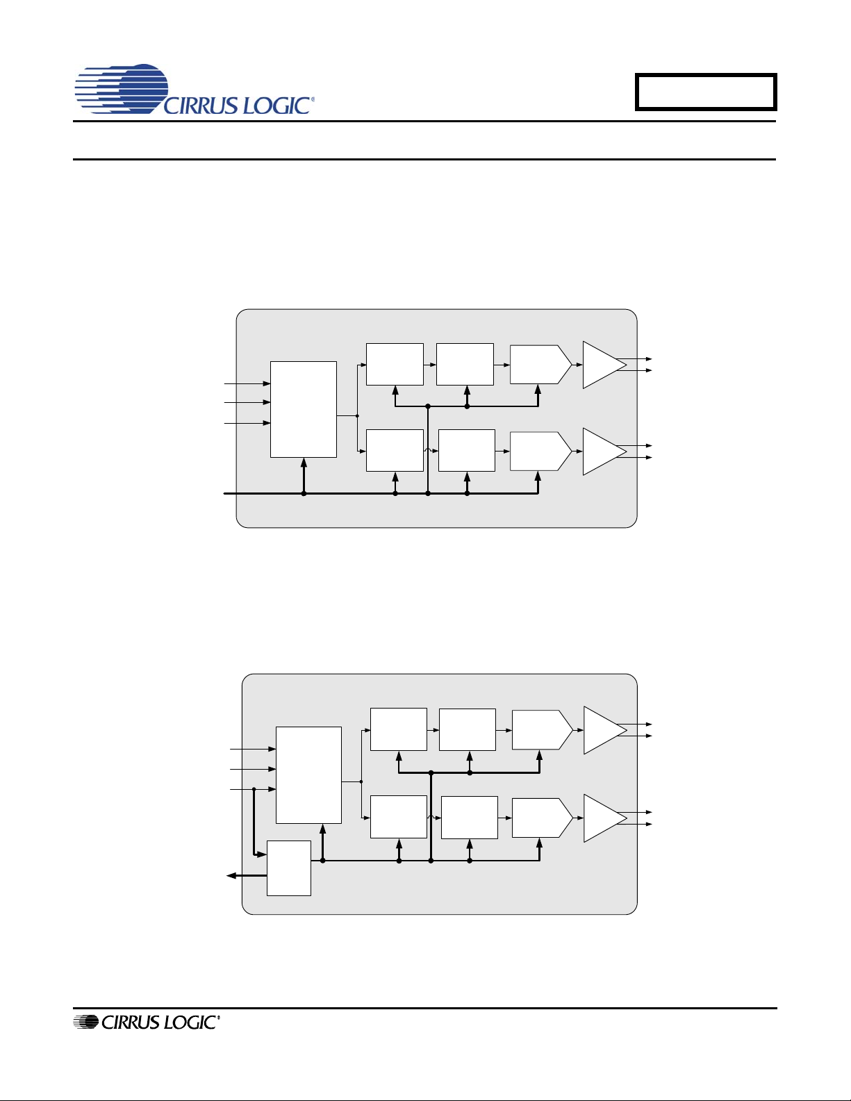
Figure 1. Typical DAC Architecture with Master Clock Input
PCM
Serial
Interface
Serial Data Input
Right
Channel
Output
Left
Channel
Output
Left-Right Clock
Recovered MCLK
Phase
Locked
Loop
Interpolation
Filter with
Volume
Control
Interpolation
Filter with
Volume
Control
Multibit ΔΣ
Modulator
Multibit ΔΣ
Modulator
Amp
+
Filter
Amp
+
Filter
DAC
DAC
Serial Clock
Internal MCLK
Figure 2. CS4350 PLL DAC Architecture
AN306
Simplifying System Design Using the CS4350 PLL DAC
1. INTRODUCTION
Typical Digital to Analog Converters (DACs) require a high- speed Master Clock to clock their digital filter s and modulators, as well as some portions of their discrete time analog circuitry. This Master Clock (or system clock) is typically required to be synchronous to the left-right (frame or word) clock (LRCK) in order to maintain sample alignment
in the digital filters, state machines, modulator and discrete time analog sections. Figure 1 below shows an example
of a typical DAC clocked by an external Master Clock. The clock is applied to the MCLK pin and then distributed to
any internal logic that requires it.
As an alternative, PLL DACs are designed to derive their internal synchronous Master Clock from some other external source. This source could be any clock, but in practice it is commonly a video clock (27 MHz) or one of the
slower SCLK or LRCK signals which are mandatory for typical PCM audio interfaces (See AN282 “The 2-Channel
Serial Audio Interface: A Tutorial”). In practice, the CS4350 PLL DAC generates its Master Clock from the input leftright clock. Figure 2 shows the CS4350 PLL DAC architecture; from the input LRCK signal, the internal PLL derives
the Master Clock signal that is used to drive the internal system timing.
The internal Master Clock generation of a PLL DAC yields inherent benefits that simplify the design of audio systems. The CS4350’s unique implementation of the feature ta kes the concept a ste p further to provide an even grea ter degree of design simplicity, flexibility, and performance.
http://www.cirrus.com
Copyright Cirrus Logic, Inc. 2009
(All Rights Reserved)
AUG '09
AN306REV1
Page 2

AN306
2. SIMPLIFIED SYSTEM DESIGN
In the design and layout of an audio mixed signal system, the conditioning and routing of the clocks are one of the
most important considerations. Because a converter’s Master Clock signal provides the sample clock that is used
as the time base for its modulator and switched ana log filters, it is typically the most sensitive to jitter and clock coupling. Eliminating the need for an external Master Clock signal provides for easier signal routing, reduced potential
for electromagnetic interference (EMI), and improved jitter immunity.
2.1 Eased Signal Routing
The Master Clock is typically generated in the digital section of a mixed signal system. This high-speed clock
then needs to be routed across the board to the an alog or mixed signal section in order to p rovide the master
clock for the converters. Since the CS4350 PLL DAC does not require a Master Clock input signal, it does
not need to be routed across the system board to re ach the conver ter. This eases the routing necessary for
the remaining clocks.
2.2 Reduced Potential for EMI
The Master Clock is typically the fastest clock used by a mixed signal audio converter. Routing any highspeed clock takes careful consideration in order to keep EMI to a minimum. The CS4350 PLL DAC provides
an easy way to ease EMI concerns by removing the dependency on the Master Clock, thus reducing the
number of high-speed clocks necessary to implement an audio subsystem.
2.3 Improved Jitter Immunity
As system designs become increasingly complex, the system clocking sources also become increasingly
complex. In many designs, the system clock is derived from a PLL within a large SOC (System on a Chip),
and is often used as the Master Clock source for the audio converters. The clocks generated from such
SOCs often exhibit high amounts of jitter, primarily as a result of the many asynchronous operations within
the SOC coupling into the clock signal. This high amount of jitter often limits the distortion (THD+N) performance and dynamic range of the mixed signal systems that use the SOC generated system clock.
Because the CS4350 PLL DAC generates its Master Clock internally, the jitter on an SOC or other system
clock source is of no consequence. When locking to LRCK, the CS4350’s PL L can reject any high-frequency
jitter that may be present on the slower LRCK.
3. LOCKING TO LRCK
The CS4350’s PLL locks to the incoming LRCK signal, and locking to LRCK provides some noteworthy advantages
over locking to another clock in the system. Specifically, locking to a system or video clock requires routing a highspeed clock to the converter and does not provide the EMI and routing advantages of locking to LRCK. Locking to
LRCK also provides for improved jitter rejection due to the lower native frequency of the left-right clock; this allows
a lower high-pass corner to be achieved in the PLL’s loop filter. When locking to LRCK, no other clocks are needed
beyond those already required in the serial PCM interface (SCLK, LRCK, and SDATA).
4. NO EXTERNAL LOOP FILTER COMPONENTS
A typical PLL consists of a phase comparator, ch arge pump, loop filte r and a VCO. The loo p filter creates an ana log
filter for the internal VCO control signal. Many PLLs require the loop filter components (typica lly two capacitors and
a resistor) to be external to the device because of internal size constraints. The CS4350 PLL uses a PLL configuration that requires no external PLL loop filter components. This allows the converter’s PLL to be self-sufficient and
also reduces the implementation cost in terms of external component price and total integration area.
2 AN306REV1
Page 3

AN306
PCM
Serial
Interface
Serial Data Input 1
Phase Locked
Loop
Left-Right Clock
Local Recovered MCLK
Serial Clock
PCM
Serial
Interface
Serial Data Input 2
PCM
Serial
Interface
Serial Data Output
CS4350
PLL DAC
DAC
ADC
SDIN1
SCLK
RMCK
LRCK
SDIN2
SCLK
LRCK
MCLK
SDOUT
SCLK
LRCK
MCLK
Long Board Traces
DSP/SOC
Figure 3. Localized MCLK using CS4350 RMCK Output
5. LOCALIZED MASTER CLOCK RECOVERY AND DISTRIBUTION
The Recovered Master Clock (RMCK) output is a unique feature of the CS4350. The RMCK output allows the
CS4350’s high-speed recovere d clock Master Clock signal to be used as the Master Clock for other more typical
audio converters that do not have built-in PLLs. Thi s feature is useful for localizing the high-speed clock to a portion
of the circuit board separate from the rest of the system, or when the integrity of a long Master Clock run could affect
the converter performance.
Figure 3 shows the CS4350 receiving only the necessary PCM clocks from a distant source while generating a re-
covered Master Clock to be used locally to the CS4350. This allows the RMCK signal recovered and provided by
the CS4350 to be used in a small area, thereby easing the system design and the routing of clocks.
Some audio converters require specific MCLK to LRCK ratios that vary according to the sample rate. The CS4350’s
RMCK output can provide this ratio variance independently from its internal Master Clock signal. This allows flexibility in the local audio converters that are using the CS4350’s RMCK output by providing a wider range of
MCLK/LRCK ratios for use.
For converters that have an automatic speed mode detection feature, no register writes are necessary to change
from 44.1 kHz to 96 kHz sample rates as the CS4350’s RMCK can be set to automatically adjust the MCLK to LRCK
ratio accordingly. See Section 4.2.1 of the CS4350 data sheet for more details on this feature.
AN306REV1 3
Page 4

AN306
Figure 4. Typical 128x DAC Out-of-Band Noise Figure 5. CS4350 Out-of-Band Noise
-150
+0
-140
-130
-120
-110
-100
-90
-80
-70
-60
-50
-40
-30
-20
-10
d
B
V
20k 120k40k 60k 80k 100k
Hz
6. OUT-OF-BAND PERFORMANCE
Converters that rely on an external Master Clock signal are often only able to operate with an internal over-sampling
rate of 128 times the sample rate (128 x Fs). This can limit the performance of the modulator by requiring the mo dulator noise shaping to begin rising at a lower frequency tha n would be possible if a higher modulator rate were a vailable.
Because the CS4350’s circuitry has access to the internal high-frequency output of the PLL, it is able to achieve a
4x higher modulator rate than typical audio converters. This allows for much lower out-of-band noise than is typically
achievable in a 128x over-sampling DAC. See Figure 4 and Figure 5 .
As a result, the CS4350 is able to achieve lower noise within much wider frequency band than many similar typical
DACs that require an external Master Clock signal. This can provide significant benefits for application s that are sensitive to noise outside of the typical 20 kHz audio band. Achieving similar out-of-band performance using a typical
128x over-sampling DAC would require high-order off-chip analo g filtering.
+0
-10
-20
-30
-40
-50
-60
d
-70
B
-80
V
-90
-100
-110
-120
-130
-140
-150
20k 120k40k 60k 80k 100k
Hz
7. CS4350 ANALOG ARCHITECTURE
The CS4350 implements a current-based DAC with on chip current-to -voltage (I-to- V) conversio n and a con tinuous
time summing amplifier. It offers both differential and single-ended analog output options with an analog supply of
3.3 V or 5 V. For design flexibility, the full-scale output reference level is set by an internal fixed reference to allow
operation with a 2 Vrms differential, or 1 Vrms single-ended output, regardless of changes to the VA supply.
8. CONCLUSIONS
The CS4350 PLL DAC offers a number of advantag es rela tive to con vention al d igital- to -a nalog co nver ters, e ach o f
which can be instrumental in simplifying the design of audio systems. From flexible output options, to localized Master Clock recovery and distribution, to low out-of-band noise performance, to system clock jitter independence, to
the easing of PCB layout and EMI concerns, the CS4350 can be called upon to solve many real-world problems of
audio system designers.
For more information about the CS4350 PLL DAC, please refer to the CS4350 datasheet available at www.cir-
rus.com.
4 AN306REV1
Page 5

REVISION HISTORY
Revision Changes
REV1 Initial Release
AN306
AN306REV1 5
Page 6

AN306
Contacting Cirrus Logic Support
For all product questions and inquiries, contact a Cirrus Logic Sales Representative.
To find the one nearest you, go to www.cirrus.com
.
IMPORTANT NOTICE
Cirrus Logic, Inc. and its subsidiaries (“Ci rrus”) believe that t he information contained in this document is accurate and reliable. However, the information is subject
to change without noti ce and is p rovided “AS IS” wit hout warran ty of any k ind (expr ess or i mplied). Customers are advis ed to ob tain the latest version of relevant
information to verify, before placing orders, that information being relied on is current and complete. All products are sold subject to the terms and conditions of sale
supplied at the time of order acknowledgment, including those pertaining to warranty, indemnification, and limitation of liability. No responsibility is assumed by Cirrus
for the use of this information, including use of this information as the basis for manufacture or sale of any items, or for infringement of patents or other rights of third
parties. This document is the property of Cirrus and by furnishing this information, Cirrus grants no license, express or implied under any patents, mask work rights,
copyrights, trademarks, trade secrets or other inte llectual property rig hts. Cirrus owns the copyrights associated with the information contained herein and gives consent for copies to be made of the information only for use within your organization with respect to Cirrus integrated circuits or other products of Cirrus. This consent
does not extend to other copying such as copying for general distribution, advertising or promotional purposes, or for creating any work for resale.
CERTAIN APPLICATIONS USING SEMICONDUCTOR PRODUCTS MAY INVOLVE POTENTIAL RISKS OF DEATH, PERSONAL INJURY, OR SEVERE PROPERTY OR ENVIRONMENTAL DAMAGE (“CRITICAL APPLICATIONS”). CIRRUS PRODUCTS ARE NOT DESIGNED, AUTHORIZED OR WARR ANTED FOR USE
IN AIRCRAFT SYSTEMS, MILITARY APPLICATIONS, PRODUCTS SURGICALLY IMPLANTED INTO THE BODY, AUTOMOTIVE SAFETY OR SECURITY DEVICES, LIFE SUPPORT PRODUCTS OR OTHER CRITICAL APPLICATIONS. INCLUSION OF CIRRUS PRODUCTS IN SUCH APPLICATIONS IS UNDERSTOOD
TO BE FULLY AT THE CUSTOMER’S RISK AND CIRRUS DISCLAIMS AND MAKES NO WARRANTY, EXPRESS, STATUTO RY OR IMPL IED, INCLUDING THE
IMPLIED WARRANTIES OF MERCHANTABILITY AND FITNESS FOR PARTICULAR PURPOSE, WITH REGARD TO ANY CIRRUS PRODUCT THAT IS USED
IN SUCH A MANNER. IF THE CUSTOMER OR CUSTOMER’S CUSTOMER USES OR PERMITS THE USE OF CIRRUS PRODUCTS IN CRITICAL APPLICATIONS, CUSTOMER AGREES, BY SUCH USE, TO FULLY INDEMNIFY CIRRUS, ITS OFFICERS, DIRECTORS, EMPLOYEES, DISTRIBUTORS AND OTHER
AGENTS FROM ANY AND ALL LIABILITY, INCLUDING ATTORNEYS’ FEES AND COSTS, THAT MAY RESULT FROM OR ARISE IN CONNECTION WITH
THESE USES.
Cirrus Logic, Cirrus, and the Cirrus Logic logo design s ar e tra de m a rks of Ci rru s Lo gi c, Inc. All o ther bra nd and product names in this document may be trademarks
or service marks of their respective owners.
6 AN306REV1
 Loading...