

Page 1
AN300
CS3001/2/11/12 & CS3003/4/13/14 Chopper-stabilized
Operational Amplifiers
Jerome E. Johnston
1. INTRODUCTION
Cirrus Logic offers a variety of low-voltage CMOS chopper-stabilized amplifiers.
The chopper-stabilized amplifiers designed at Cirrus Logic are unique. These amplifiers offer performance benefits
that combine the best features of bipolar amplifiers with the best features of chopper amplifiers. The intent of this
application note is to understand Cirrus Logic's unique technology and to see how it can be applied in various measurement applications. But before the applications are discussed, the following provides a brief overview of the concepts involved in a chopper-stabilized amplifier.
2. CHOPPER AMPLIFIER AND CHOPPER-STABILIZED AMPLIFIER BASICS
Not everyone is familiar with chopper amplifiers and chopper-stabilized amplifiers. A look back at some history can
help us understand how the chopper-stabilized amplifier operates.
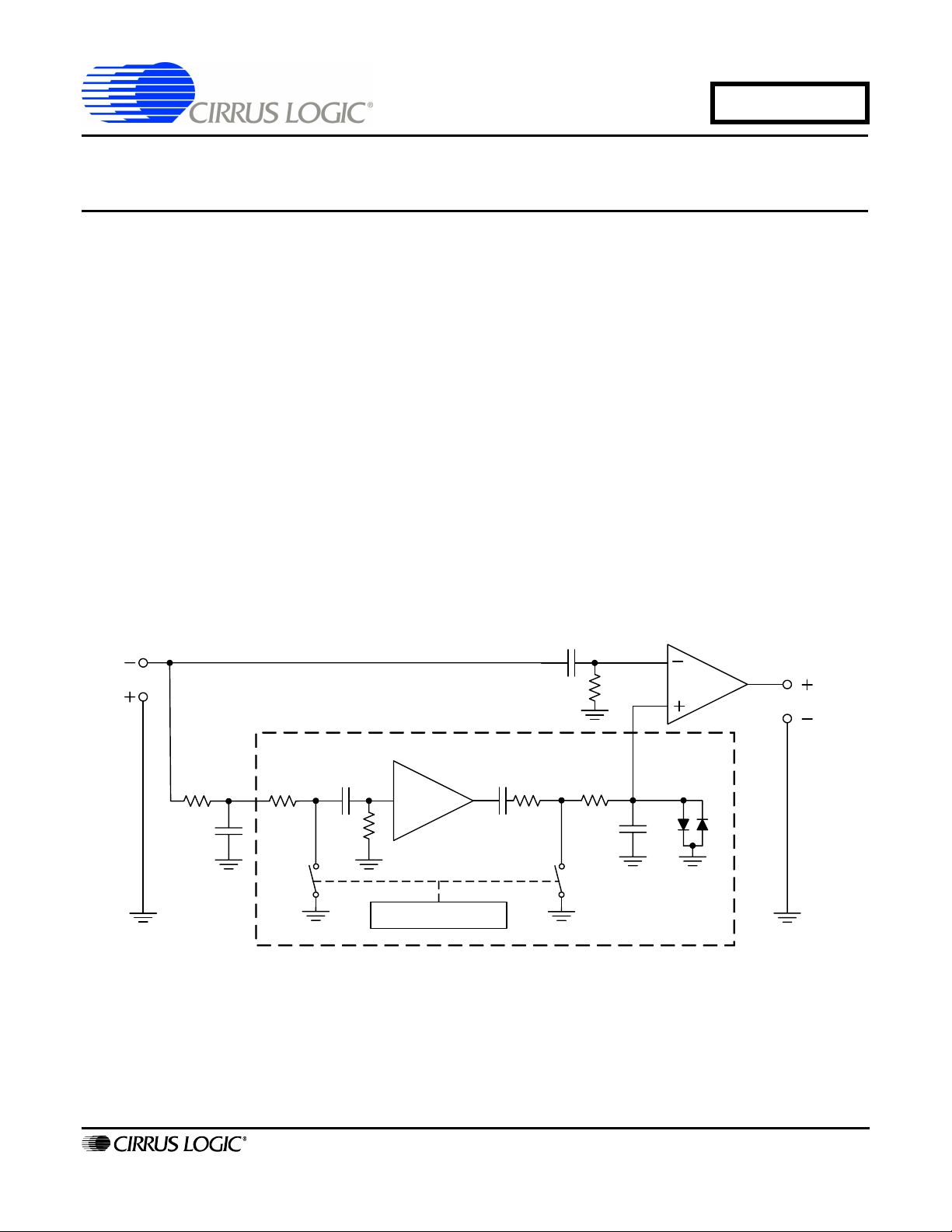
Figure 1 illustrates the block diagram of a chopper-stabilized amplifier. A chopper-stabilized amplifier is a DC am-
plifier whose offset is stabilized by a chopping amplifier. The basic amplifier diagram in Figure 1 is called the Goldberg configuration, named after E. A. Goldberg, an engineer who designed and patented electron tube-based,
chopper-stabilized amplifiers for RCA (Radio Corporation of America) in the 1940s and 1950s.
DC Amplifier
e
in
C1
R1
AMP1
e
out
AC Amplifier (Chopper)
C3
AMP2
R3R2
C2
Figure 1. Basic Chopper-stabilized Amplifier Block Diagram
The Goldberg configuration was later used in a transistorized chopper-stabilized amplifier designed and sold
by Zeltex Corporation in the 1970s for about $125 (US). The Zeltex chopper-stabilized amplifier follows the basic
block diagram of Figure 1. The input signal (e
signal paths. (The Goldberg configuration amplifier could only be used as an inverting amplifier.) The first path is
into Amplifier #1 of Figure 1. Components R1-C1 act as a high-pass filter that prevents the DC portion of the signal
from passing directly into Amplifier #1. The second path is through a low-pass filter composed of R2 and C2. The
R2-C2 filter limits the bandwidth of the signal to be chopped by the chopper amplifier. Amplifier #2 is the chopper
R4
Oscillator
) at the inverting input of the amplifier travels through two different
in
C4
Low-pass
R6
Filter
R5
C5
S2S1
http://www.cirrus.com
Copyright © Cirrus Logic, Inc. 2008
(All Rights Reserved)
JUL ‘08
AN300REV1
Page 2
AN300
amplifier. The chopper amplifier is really a modulation system in which the DC and very low-frequency portion of the
input signal is alternately turned on and off. This results in the signal being modulated at the carrier (chopping) frequency. An oscillator in the chopper amplifier toggles switches S1 and S2 on and off simultaneously. When switch
S1 is conducting, the input to the chopper amplifier is ground. When switch S1 is off, the input signal is allowed to
pass into Amplifier #2. The effect of chopping is to turn the DC input signal into a square wave (AC) signal whose
amplitude changes between ground and the amplitude of the input signal. This signal is then amplified by the AC
amplifier. Once the signal is amplified as an AC signal, it is restored to ground reference by the output chopping
switch. This resulting signal, which is a ground-referenced square wave, is then filtered with a low-pass filter composed of resistors R5 and R6 in conjunction with capacitor C5. The corner frequency of this filter is very low – typically only fractions of a Hertz. The time constant must be very long to maintain the voltage on the filter capacitor
over the half cycle when the chopped signal is not presented to the output filter.
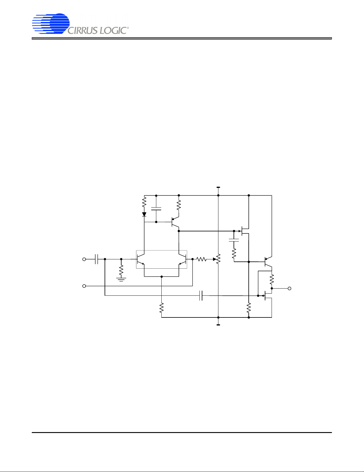
Figure 2 illustrates the DC amplifier portion of the Zeltex device. This amplifier was constructed with a matched bi-
polar transistor pair as the front end. The open loop gain of the DC amplifier is about 94 dB.
Figure 3 illustrates the actual chopper amplifier portion of the Zeltex amplifier. The amplifier AC gain is about 3000,
but because the signal is on only 50% of the time, the effective gain is only half as much. Therefore the AC amplifier
gain is about 1500, or about 63 dB. The chopping oscillator operates at about 200 Hz. Note that the chopper output
is filtered by a low-pass filter with an extremely low corner frequency.
+15V
-IN
From AC
Amplifier
51k
1N459
26
C1
0.1uFR1200k
0.005uF
17
2N2914
35
51k
2N4248
10M
500k 56k
10pF
2.4k
100k
-15V
Figure 2. Amplifier 1: DC Amplifier Portion of the Zeltex Module
E304
2N4248
680
OUT
2 AN300REV1
Page 3
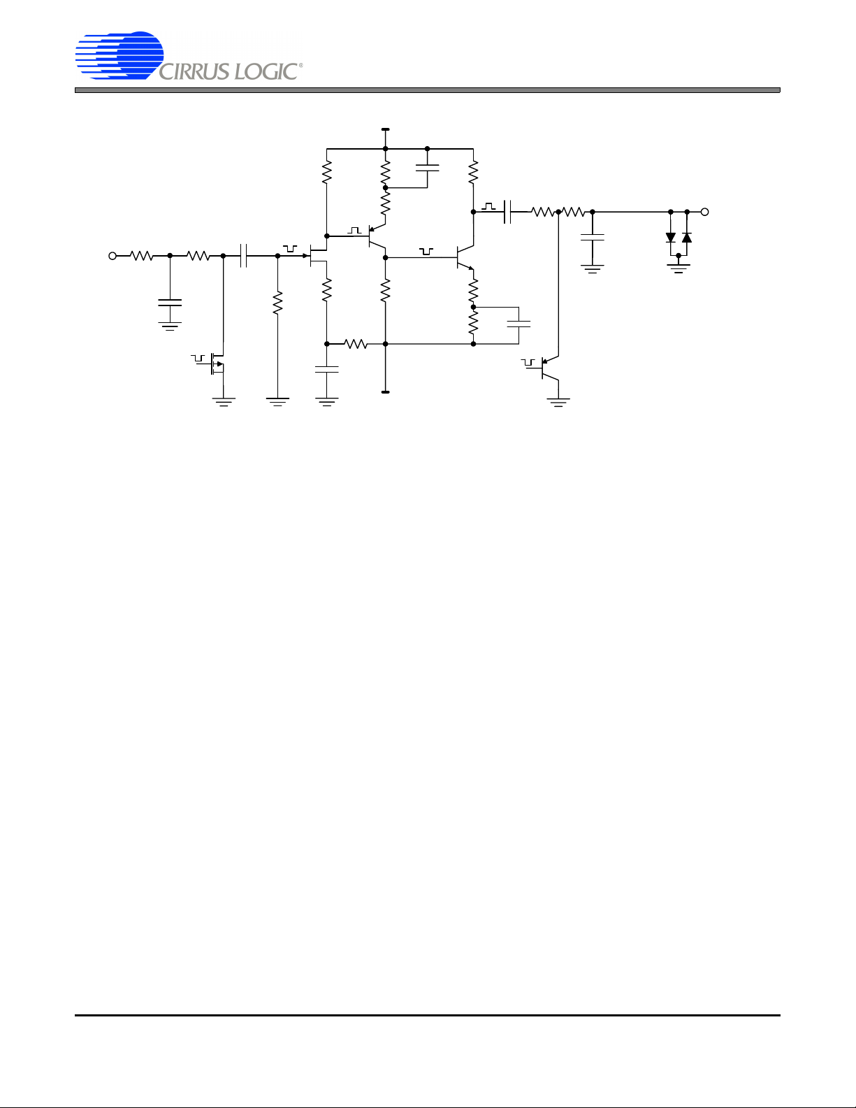
+15V
AN300
10k
150
2N4299
10k
22uF
150
10k
51k
C4
0.033uF
2N3565
22uF
From
Oscillator
R6
51kR5200k
S2
2N2946
fc = 0.009Hz
C5
1N459
68uF
To DC
1N459
R2
100k
From
Oscillator
R3
100k
C2
0.033uF
C3
4700pF
S1
M5079
R4
2.0M
3.9k
E305
1k
18k
68uF
-15V
Figure 3. Amplifier 2: Chopper Amplifier Portion of the Zeltex Module
The gain transfer functions of the two amplifiers are multiplied together (or added when stated in dB). The combination of the two amplifiers produces an open loop gain of about 160 dB. One of the difficulties in the design of the
chopper-stabilized amplifier combination is ensuring stability. The DC performance of the combined amplifiers is dictated by the performance of the chopping input. Input current of the Zeltex amplifier was dominated by charge injection in the chopping switch at the input of the chopper amplifier. Offset voltage and offset voltage drift of the amplifier
combination was determined by how close the chopping switch at the input of the chopper amplifier approximated
the ideal. The Zeltex amplifier achieved less than 100 pA of input bias current with an offset voltage drift less than
50 nV / °C.
Figure 4 illustrates a typical chopper-stabilized amplifier designed using electron tubes with the amplifiers connected
in the Goldberg configuration. The circuit has the same layout as the block diagram of Figure 1. The chopping
switches were mechanical vibrating switches (about 400 Hz) manufactured by Airpax Corporation. The output filter
exhibits an extremely long time constant.
E.A. Goldberg filed a U.S. patent (#2,684,999; assigned to RCA) for a tube-based chopper-stabilized amplifier on
April 28, 1948. But the invention of the chopper architecture itself predates this. J. W. Milnor filed for a U.S. patent
on a chopper amplifier on January 17, 1918.
AN300REV1 3
Page 4
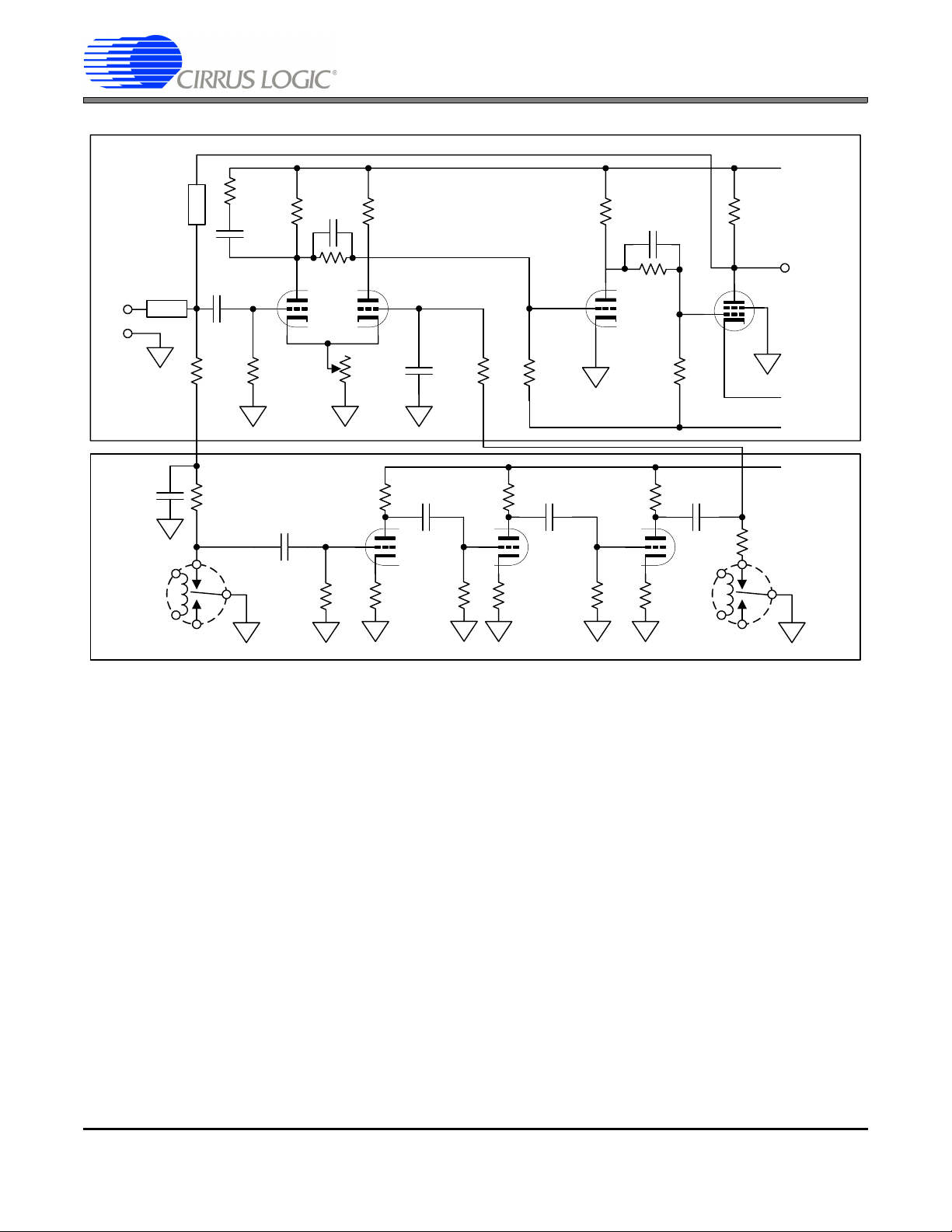
DC Amp
AN300
R2
330
C4
3nF
R8
220k
Z
f
C2
350pF
100k
220k
C3
10pF
+300V
10k
e
IN
C5
0.01uF
AC Amp
Figure 4. Chopper-stabilized Amplifier Using Electron Tubes and Mechanical Vibrating Swit ches
680k
C1
R3
10k
2uF
R1
10M
5751
R7
1k
Z
i
fc = 0.008 Hz
C6
2uF
R4
10M
V2A
2M
2.2M
½ 5751
760k
Output
6AQ5
-250V
-400V
+300V
R5
2.2M
C7
0.01uF
2.2M
R6
1k
220k
0.1uF
5751
220k
0.1uF
1M 1M 1k
1k
220k
½ 5751
0.1uF
1k
NOTE: 5751 = Ruggedized 12AX7.
3. MODERN CHOPPER-STABILIZED AMPLIFIERS
Monolithic chopper-stabilized amplifiers became available in the late 1970s. Different chopping architectures have
been promoted by various vendors. The various architectures will not be examined in detail here. Before discussing the particulars of the Cirrus Logic chopper-stabilized amplifiers, it will be beneficial to understand some differences found in bipolar versus MOS transistors.
For many years bipolar transistors dominated monolithic amplifier designs. Bipolar transistors have some distinct
advantages over CMOS transistors for some performance parameters. The bipolar transistor provides higher
transconductance (I/V gain) for a specific value of operating current. The bipolar device, because of its construction, also provides lower noise than can easily be achieved in a MOS transistor, for devices of similar silicon area.
The wide band spot noise level is lower in the bipolar transistor. And a much lower 1/f noise corner can be
achieved in a bipolar transistor. Bipolar transistors can also be better matched when manufactured together on the
same silicon die.
Most recently, the most prominent semiconductor processes being developed to shrink the geometry size of
devices is being applied to CMOS technology. CMOS is favored because it can provide lower power consumption
for massive digital chips with millions of transistors. Smaller transistors mean the availability of more transistors in
a given area of silicon. This results in smaller device package sizes. In the last decade, more analog and mixed
signal devices have been designed to take advantage of the smaller geometry CMOS processes. This includes
monolithic amplifiers based upon CMOS processes.
4 AN300REV1
Page 5
AN300
As mentioned previously, bipolar transistors have long dominated the world of operational amplifiers. Let's look at
some of the differences of parameters of bipolar transistors versus MOS transistors. Understanding the differences between these two technologies can help explain some of the constraints on the architectural choices used
in the design of CMOS chopper-stabilized amplifiers.
The construction of bipolar transistors and MOS transistors are very different. The difference in construction results
in large differences in some performance parameters. One area of significant difference is noise performance.
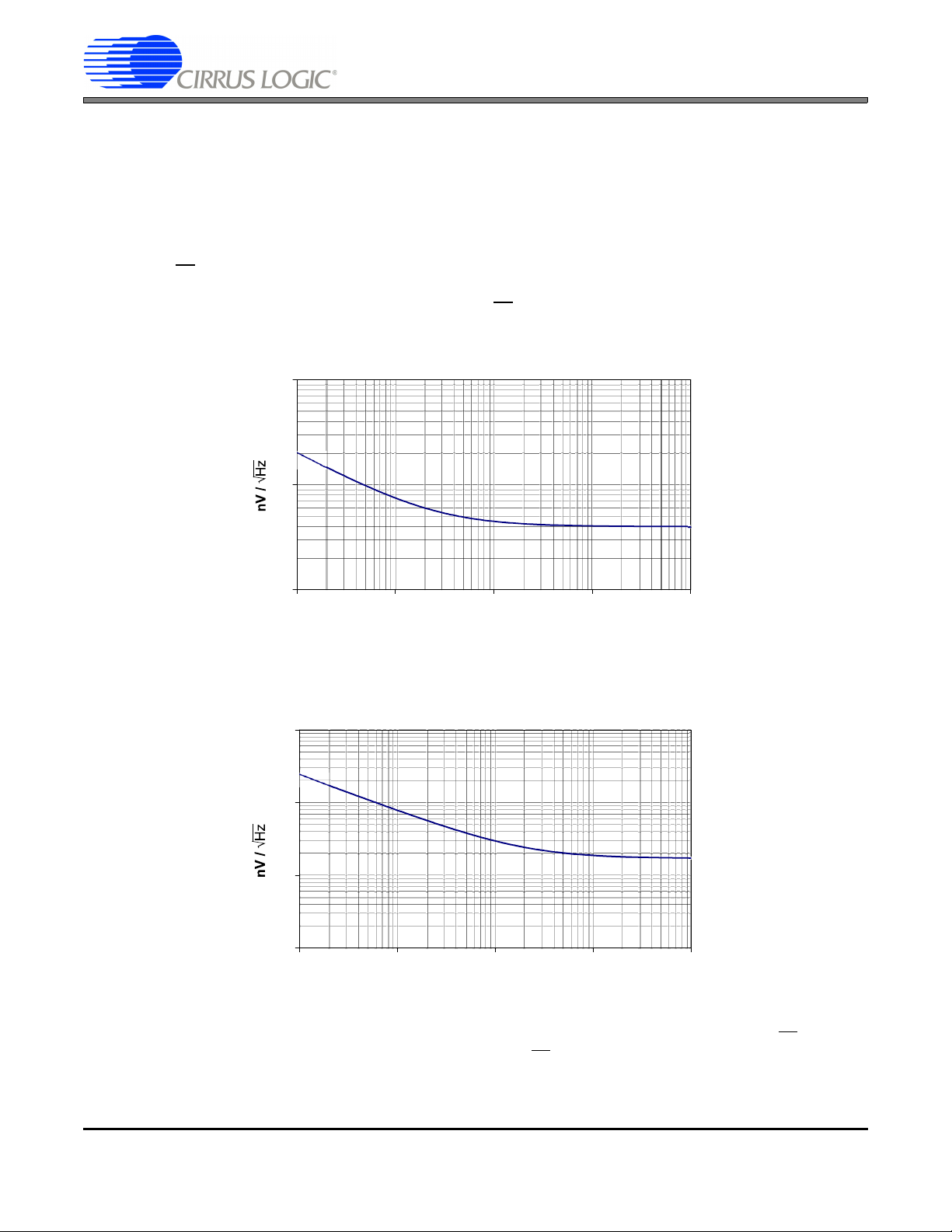
Figure 5 illustrates a noise plot for a bipolar transistor. This hypothetical but typical device exhibits a spot noise at 1
kHz of 4 nV/√Hz
difficulty achieving this level of noise performance. Figure 6 illustrates a noise plot for a hypothetical but typical
MOS transistor. This device exhibits a spot noise of 17 nV/√Hz
with a 1/f corner at 2.5 Hz. Because of the difference in construction, a MOS transistor would have
at 50 kHz with a 1/f corner at 2000 Hz.
Bipolar Transistor Noise
100
10
1
0.1 1 10 100 1k
Figure 5. Noise Performance Plot for a Bipolar Transistor
Frequency (Hz)
MOS Transisitor Noise
1000
100
10
1
10 100 1k 10k 100k
Frequency (Hz)
Figure 6. Noise Performance Plot for a MOS Transistor
Note from Figure 5 that the magnitude of the noise of the bipolar transistor at 0.1 Hz is about 20 nV/√Hz. The spot
noise in the example MOS transistor does not match this 20 nV/√Hz
value until the frequency for the MOS transistor is at about 5 kHz. A MOS transistor can be designed to achieve a lower spot noise and a lower 1/f corner frequency than what is shown in Figure 6 by significantly increasing the size of the device and by increasing its
AN300REV1 5
Page 6

AN300
operating current. But there is another approach to achieve low noise in a CMOS amplifier. That is to modulate
(chop) the input signal and amplify the signal as an AC signal at a frequency that is significantly higher than the 1/f
corner frequency. If the chopping is performed at a higher frequency where the spot noise is low, the noise floor will
be dictated by the noise value at the chopping frequency. The chopper-stabilized amplifiers from Cirrus Logic use
this approach. Most chopper amplifiers from other manufacturers chop at lower frequencies, where the spot noise
is higher. Some choppers even chop in the region of the rising 1/f noise.
Cirrus Logic manufactures amplifiers having different chopper-stabilized architectures. The CS3003/4/13/14 amplifiers are similar to the architecture shown in Figure 1, but with the design optimized for silicon implementation. A
block diagram of these devices is illustrated in Figure 7. The chopping frequency in the CS3003/4 devices is at
about 150 kHz. The CS3013/14 chopping frequency is at about 125 kHz. The filter at the output of the chopping
amplifier is on chip where capacitor sizes are limited. A higher chopping clock is more easily filtered when capacitor
size of the filter must be a small value. These amplifiers combine chopper-stabilized input performance with rail-torail input and rail-to-rail output capability. Even though these amplifiers are chopped, they can be used for audiobandwidth applications because no chopping clock residuals exist below 100 kHz.
E
in
Σ
Σ
E
out
≈ 60 dB
≈ 100 dB
Figure 7. Block Diagram of Cirrus Logic’s Chopper-stabilized Amplifier, CS3003/04/13/14
Figure 8 illustrates the open loop gain and phase of the CS3003/04 amplifiers. One can readily see from the plot
that the transition point between the chopper amplifier signal path and the high frequency signal path cross over
near 20 kHz.
180
160
140
120
100
80
60
40
20
0
-20
0.001 0.1 10 1k 100k 10M0.01 1 100 10k 1M
Frequency (Hz)
270
225
180
135
90
45
0
-45
-90
-135
-180
Figure 8. CS3003/04 Gain & Phase vs. Frequency
Recall that the gains of the amplifier stages add together (in dB). The combination requires careful design to maintain stability and to achieve the proper frequency crossover between the two signal paths. But the result is an
amplifier with very high open loop gain.
The CS3001/2/11/12 amplifiers differ architecturally from the CS3003/04/13/14 devices. The CS3001/2/11/12
amplifiers have more signal paths than the typical chopper-stabilized amplifier. Figure 9 illustrates the signal paths
6 AN300REV1
Page 7

AN300
inside the Cirrus Logic CS3001/2/11/12 amplifiers. Note that although not shown in the diagram, the signal is
chopped as a differential signal.
V
IN
Figure 9. Block Diagram of Cirrus Logic’s Multipath Chopper-stabilized Amplifier, CS3001/02/11/12
AMP1
φ1
High-frequency Path
φ1
AMP2
AMP3
AMP4
AMP5
V
OUT
The "multi-path" approach to these amplifiers was used to achieve 300 dB of open loop gain. These amplifiers can
be made stable for gains higher than 50X with a single feedback capacitor. They offer significant improvement over
competing amplifiers when an amplifier with low noise, low offset drift and very high open loop gain is required for
an application. Figure 10 illustrates the open loop gain and phase of the CS3001/2/11/12 amplifiers. Figure 11 illustrates an expanded view of the region of the open loop gain and phase above 10 kHz.
Gain
Phase
Figure 10. Open-loop Gain and Phase vs. Frequency, CS3001/02/11/12
AN300REV1 7
Page 8

100
80
60
40
20
0
-45
-90
-135
-180
-225
-270
-315
-360
10K
100K
1M
10M
Figure 11. Open-loop Gain and Phase vs. Frequency, CS3001/02/11/12 (Expanded)
AN300
In applications that require a small signal (< 10 mV) to be amplified by a large gain (> 200X) the very high open
loop gain of the CS3001/2/11/12 amplifiers ensures gain accuracy and excellent linearity. Figure 12 compares the
open loop gain of the CS3001 to an operational amplifier with 120 dB of open loop gain where the amplifiers are
configured for a gain of 400X (52 dB). If the CS3001 is configured for a gain of 400X (52 dB), the amplifier has 248
dB of loop gain (300 - 52 = 248) to ensure gain accuracy and to reduce linearity errors. 248 dB is a factor of 2500
billion. This appears to be excessive until one understands that the CS3001 was designed to achieve 20-bit linearity with a 1 kHz sine wave when set for a closed loop gain of 30X.
8 AN300REV1
Page 9

AN300
52
300
280
260
240
220
200
180
160
140
120
100
80
60
40
20
CS3001
Loop Gain = 300 - 52 = 248
Typical Op Amp
Gain = 120 - 52 = 68
ACL
Gain = 52 (400X)
0
-20
0.1 10 1k 100k 10M0.01 1 100 10k 1M
Frequency (Hz)
Figure 12. Open Loop Gain Comparison
If an operational amplifier with only 120 dB of open loop gain is configured for a forward gain of 400X (52 dB). This
leaves only 68 dB of loop gain. A loop gain 68 dB is a factor of about 2500. Therefore, this amplifier set for a closed
loop gain of 52 dB, would be able to reduce open loop linearity error by a factor of 2500. This factor is a billion
times less (that is 1,000,000,000 times less) than what the CS3001 can achieve in the same configuration.
AOL = Open Loop Gain.
AN300REV1 9
Page 10

AN300
Figures 13 and 14 illustrate the noise performance of the CS3001/2 amplifiers. Figure 13 illustrates the extreme
low-frequency noise performance of the CS3001/2. This plot is based upon a real measurement taken over an 18
hour period. Have you ever seen a data sheet for an operational amplifier from another vendor show a plot of noise
below 0.1 Hz? Unlikely, because 0.1 Hz is arbitrarily considered the point of transition between examining the
effects of 1/f noise versus the effects of offset drift due to temperature changes. This plot is possible for the
CS3001/2/11/12 series amplifiers from Cirrus Logic only because of the very low drift due to chopping along with
low-noise performance.
Figure 13. CS3001/02 Low-frequency Noise (Measured)
Figure 14 illustrates the noise behavior of the CS3001/2 as the frequency increases above 2 kHz. The CS3001/2
devices are designed to be used for low frequency (less than 2 kHz) applications. The CS3001/2 design achieves
a significant reduction in power consumption by lowering the operating current of the last amplifier stage. This compromise causes the noise in the device to rise at frequencies above 2 kHz. This noise can be removed by filtering.
Some delta-sigma A/D converters have digital filters that can remove the noise above 2 kHz.
Figure 14. CS3001/02 Wideband Noise
10 AN300REV1
Page 11

AN300
Figure 15 illustrates the offset stability of the CS3001/2 over time. This plot was based upon band limiting the
amplifier to 3.2 Hz and measuring the amplifier output for an hour. The fact that the plot of the statistical distribution of the noise out of the amplifier over an hour remains Gaussian validates that the offset of the amplifier is not
moving over the time period.
100
75
= nVσ
σ = 13 nV
50
25
0
nV
-25
-50
-75
-100
Time (1 Hour)
Figure 15. Offset Voltage Stability (DC to 3.2 Hz)
The CS3001/2/11/12 and CS3003/4/13/14 devices all use chopping clock frequencies greater than 100 kHz. This
allows the clock to be more easily filtered on-chip.
Table 1 summarizes the typical amplifier specification parameters for the Cirrus Logic's chopper-stabilized amplifi-
ers.
AN300REV1 11
Page 12

Comments
Freq.
Chop
R-to-R
Output
Input
R-to-R
/Ch
q
(mA)
I
Range
Supply
AN300
Bandwidth
2 kHz Usable
Bandwidth
2 kHz Usable
Bandwidth
1 kHz Usable
Bandwidth
1 kHz Usable
Table 1. Typical Specifications for Cirrus Logic Chopper-stabilized Amplifiers
Drift
VOS
0.1 to 10 Hz
Voltage
AVOL
Slew Rate
(V/°C)
(V)
bias
I
Noise
Noise
(dB)
(V/ S)
125nV p-p
6nV/√Hz
100 10 0.01 2.7 to 6.7 2.100 N Y 180 kHz
@10Hz
@0.5Hz
125nV p-p
6nV/√Hz
100 10 0.01 2.7 to 6.7 1.800 N Y 180 kHz
50 10 0.01 2.7 to 6.7 0.900 N Y 180 kHz
250nV p-p
12nV/√Hz
50 10 0.01 2.7 to 6.7 0.850 N Y 180 kHz
170 10 0.05 2.7 to 5.5 0.500 Y Y 125 kHz
170 10 0.05 2.7 to 5.5 0.500 Y Y 125 kHz
@10Hz
@10Hz
@10Hz
250nV p-p
460nV p-p
@0.5Hz
@0.5Hz
12nV/√Hz
22nV/√Hz
@10Hz
460nV p-p
@0.5Hz
@0.5Hz
22nV/√Hz
170 10 0.01 2.7 to 5.5 1.000 Y Y 150 kHz
170 10 0.01 2.7 to 5.5 1.000 Y Y 150 kHz
@10Hz
@10Hz
350nV p-p
@0.5Hz
17nV/√Hz
@10Hz
350nV p-p
@1Hz
@0.5Hz
17nV/√Hz
Device Amps GBW
3001 14MHz 5 300
3002 24MHz 5 300
3003 12MHz0.25 150
3004 22MHz0.25 150
3011 12MHz 2 300
3012 22MHz 2 300
3013 11MHz0.25 135
3014 21MHz0.25 135
12 AN300REV1
Page 13

AN300
4. APPLICATION CIRCUITS
4.1 Thermopile Amplifiers
Figures 16 illustrates a basic diagram of a thermopile. The thermopile is a collection of series-connected thermo-
couples designed to detect spectral radiation. The spectrum of light is first filtered by an optical filter to select the
frequency of light that is to be measured. This light passes through the optical filter and strikes an energy absorbent
coating that converts the light into heat. The thermal change due to the absorbed radiation then causes a change
in the output voltage of the series-connected thermocouples. The resultant output voltage is usually very small and
must be amplified. The magnitude of the output signal is affected by the sensor area, the sensor technology, the
filter optics, and the last of all, the intensity of the radiation.
Figure 16. Typical Thermopile Block Diagram
A wide variety of thermopile devices are available. Various thermopile manufacturers offer thermopiles based upon
thin film technology or upon silicon technology. Thin film devices tend to have lower noise and provide higher sensitivity. Silicon devices are less sensitive and have higher noise levels, but provide better temperature stability. Silicon devices are also less expensive.
Optical Filter
Aperture
Active Area
15 “Hot” (Active Area) Junctions
“Cold” Junctions
G
N
D
T
U
O
V
Alternating “Arms” of
Antimony & Bismuth
Images courtesy of Dexter Research Center, Inc.
Terminal Connections
Figure 17. Typical Thermopile & Junction Layout
AN300REV1 13
Page 14

AN300
Figure 18 illustrates a thermopile amplifier set for a gain of 640 V/V. The Dexter Research 1M thermopile is a thin
film device that exhibits a typical thermal noise of 7 nV/√Hz
output only a few millivolts of signal. The CS3001 operational amplifier provides very high open loop gain and a low
spot noise of 6 nV/√Hz
. The circuit can readily amplify a 5 mV signal to several volts.
Dexter Research
Thermopile 1M
. In a typical infrared sensing application, the device may
CS3001
R2
64.9k
R1
100
C1
0.015µF
Figure 18. Thermopile Amplifier with Gain of 650 V / V
The thermopile, like the thermocouple, must be “cold junction” compensated. This would require a second sensor
on the thermopile for this function. Manufacturers of thermopile sensors generally offer devices that include a sensor
for cold junction sensing. This second sensor necessary for cold junction correction is not shown in Figure 18.
4.2 Load Cell Amplifiers
Load cells output small signals, typically less than 10 mV. To maintain high signal to noise, this small signal must
be amplified with a low noise, low drift, high gain amplifier.
Cirrus Logic's chopper-stabilized amplifiers are very suitable for this type of application.
The combination of the CS3001 amplifier and the CS5512 A/D converter can provide a high resolution digitizer for
a load cell as shown in Figure 19.
+5 V
1 mV/V
350 Ω
88.7 kΩ
0.1 µF
0.1 µF
0.47 µF
71.5 kΩ
-+
CS3001
-
+
100 Ω
VREF
0.1 µF
200 Ω
0.047 µF
200 Ω
AIN1
V+
CS
SDO
SCLK
CS5510/12
AIN+
V-
+5 V
µC
Counter/Timer
Figure 19. High-resolution Digitizer for a Load Cell
The CS3001 amplifier exhibits low noise, low drift, and incredibly high open loop gain.
14 AN300REV1
Page 15

AN300
The circuit illustrates the CS3001 with a gain of negative 408X. Note that the negative output from the bridge is connected to the inverting amplifier input. This results in a positive output from the amplifier into the A/D converter. The
amplifier gain is set by the 71.5K and the parallel combination of the two 350 ohm resistors inside the bridge, or 175
ohm. The 88.7 K resistor offsets the bridge (offset is about +4.9 mV at the minus output side of the bridge) to allow
the input of the A/D to be negative (about -2 V) with no weight on the load cell. The full input span of the A/D is
nominally +/-4 V fully differential, as set by the 5 V on the VREF pin. Adding offset to the bridge output allows use
of the negative range of the A/D and provides more codes out of the converter for the full output span of the bridge
signal. When the full load is applied to the load cell, it will output approximately 5 mV.
The circuit shows the CS5510/12 devices, but the CS5511/13 devices can also be used.
The circuit in Figure 19 has the disadvantage that when full load is applied to the bridge, the inverting amplifier output
current (2 V / 71.5 k, or about 28 microamperes) must flow through the 71.5 k resistor and into the inverting signal
connection of the bridge. Therefore the inverting side of the bridge sees a different magnitude of current than the
non-inverting side. This imbalance may introduce a signal dependent offset in the bridge due to different temperature effects on the bridge elements. This can limit the overall accuracy of the measurement.
Figure 20 illustrates a different load cell amplifier configuration than Figure 19. Using the CS3002, this amplifier con-
figuration yields high impedance to both the plus and minus outputs of the load cell. The high impedance permits
the use of the 1 kΩ & 300 pF components to prevent the effects of RFI (radio frequency interference).
+5 V
-
1 mV/V
350 Ω
1 kΩ
+
R3
(86.6 kΩ)
CS3002
300 pF
+
-
R2
140 k Ω
-
1 kΩ
300 pF
+
X715
(X1419 )
0.1 µF
R1
392 Ω
(196 Ω )
R2
140 kΩ
C1
0.22 µF
C2
0.22 µF
100 Ω
0.1 µ F
200 Ω
0.047 µF
200 Ω
VREF
CS5510/12
AIN+
AIN-
V+
CS
SDO
SCLK
V-
+5 V
µC
Counter/Timer
Figure 20. Digitizer for a Load Cell with High-impedance Inputs
In this schematic, the load cell has a sensitivity of 1 mV/V and outputs only about 5 mV under full load. The schematic illustrates two different gain configurations. If the bridge is used without being offset by resistor R3, the amplifier gain is set for 715X. The output of the amplifier (the input to the A/D) will change from about 0 volts (differential)
to about 3.575 volts (differential) when the load on the load cell goes from zero to full load.
By adding resistor R3, the bridge is offset by about 5 mV. This causes the input to the A/D to be at -3.6 volts (differential) when no weight is on the scale. The amplifier gain is set for 1419X by changing the value of R1,and produces
a change of about 7.1 volts, differential at the input of the A/D when the load on the load cell changes from zero to
full load. The circuit will achieve about 27,000 noise-free counts on a 5 mV signal.
The noise in this circuit will be limited by the amplifier noise. Changing C1 & C2 to 0.47 µF can increase performance
to about 38,000 noise-free counts. Again, averaging can greatly improve the number of useful counts from the circuit.
For more information about similar weigh-scale circuits, including some discussion about noise performance, please
refer to Cirrus Logic Application Note AN330, Load Cell Measurement using the CS3001/02/11/12 Amplifiers with
the CS5510/11/12/13 A/D Converters.
AN300REV1 15
Page 16

AN300
Contacting Cirrus Logic Support
For all product questions and inquiries, contact a Cirrus Logic Sales Representative.
To find the one nearest to you, go to http://www.cirrus.com
IMPORTANT NOTICE
Cirrus Logic, Inc. and its subsidiaries ("Cirrus") believe that the information contained in this document is accurate and reliable. However, the information is subject
to change without notice and is provided "AS IS" without warranty of any kind (express or implied). Customers are advised to obtain the latest version of relevant
information to verify, before placing orders, that information being relied on is current and complete. All products are sold subject to the terms and conditions of sale
supplied at the time of order acknowledgment, including those pertaining to warranty, indemnification, and limitation of liability. No responsibility is assumed by Cirrus
for the use of this information, including use of this information as the basis for manufacture or sale of any items, or for infringement of patents or other rights of third
parties. This document is the property of Cirrus and by furnishing this information, Cirrus grants no license, express or implied under any patents, mask work rights,
copyrights, trademarks, trade secrets or other intellectual property rights. Cirrus owns the copyrights associated with the information contained herein and gives consent for copies to be made of the information only for use within your organization with respect to Cirrus integrated circuits or other products of Cirrus. This consent
does not extend to other copying such as copying for general distribution, advertising or promotional purposes, or for creating any work for resale.
CERTAIN APPLICATIONS USING SEMICONDUCTOR PRODUCTS MAY INVOLVE POTENTIAL RISKS OF DEATH, PERSONAL INJURY, OR SEVERE PROPERTY OR ENVIRONMENTAL DAMAGE (“CRITICAL APPLICATIONS”). CIRRUS PRODUCTS ARE NOT DESIGNED, AUTHORIZED OR WARRANTED FOR USE
IN PRODUCTS SURGICALLY IMPLANTED INTO THE BODY, AUTOMOTIVE SAFETY OR SECURITY DEVICES, LIFE SUPPORT PRODUCTS OR OTHER CRITICAL APPLICATIONS. INCLUSION OF CIRRUS PRODUCTS IN SUCH APPLICATIONS IS UNDERSTOOD TO BE FULLY AT THE CUSTOMER’S RISK AND CIRRUS DISCLAIMS AND MAKES NO WARRANTY, EXPRESS, STATUTORY OR IMPLIED, INCLUDING THE IMPLIED WARRANTIES OF MERCHANTABILITY AND
FITNESS FOR PARTICULAR PURPOSE, WITH REGARD TO ANY CIRRUS PRODUCT THAT IS USED IN SUCH A MANNER. IF THE CUSTOMER OR CUSTOMER’S CUSTOMER USES OR PERMITS THE USE OF CIRRUS PRODUCTS IN CRITICAL APPLICATIONS, CUSTOMER AGREES, BY SUCH USE, TO FULLY
INDEMNIFY CIRRUS, ITS OFFICERS, DIRECTORS, EMPLOYEES, DISTRIBUTORS AND OTHER AGENTS FROM ANY AND ALL LIABILITY, INCLUDING ATTORNEYS’ FEES AND COSTS, THAT MAY RESULT FROM OR ARISE IN CONNECTION WITH THESE USES.
Cirrus Logic, Cirrus, and the Cirrus Logic logo designs are trademarks of Cirrus Logic, Inc. All other brand and product names in this document may be trademarks
or service marks of their respective owners.
16 AN300REV1
 Loading...