

Page 1
AN299
Optimizing the Performance of CS553x ADCs
1. INTRODUCTION
Getting optimum performance with high-performance converters is not a trivial task. Good system grounding techniques, power supply filtering, careful board layout, and control of system clocks and high-speed digital signals is of
utmost importance. We will cover these and other subjects in this application note in order to allow your design to
get the best performance from the CS5531/2/3/4 converters.
The CS5531/2/3/4 family of Delta-Sigma converters are some of the lowest-noise DC measurement devices in the
market. These devices are suitable for many applications where high-resolution measurements of very small DC
voltages are required, such as weigh scales, pressure transducers, and thermocouples. With a built in, low-noise,
programmable gain amplifier, the full-scale input range can be as low as 39.0625 mV DC in unipolar mode with a
2.5 V or 5 V VREF. As will be demonstrated in this application note, the input scale can be reduced even further,
allowing very small differential inputs to be measured to a high degree of resolution. For example, as explained in
this document, a 10 mV full-scale unipolar input can be measured to 0.596 nV per least-significant bit with the 24bit devices. Obviously the output will contain noise, but with software averaging, that noise can be resolved to an
impressive number of noise-free bits.
2. THE IMPORTANCE OF A GOOD GROUND PLANE
In order to reduce board costs, some designs may attempt to use single- or double-sided boards and fill unrouted
areas with a ground plane. Please be aware that this is not an effective practice in a high-performance analog-todigital conversion circuit. A low-noise, low-impedance, uninterrupted ground plane is extremely important in order
to get optimum performance from the ADC. However, filling unused areas around the input traces with copper and
connecting that copper to the ground plane does have some additional advantages regarding Faraday shielding.
The ground plane is the point of reference for many signals on the board. The extremely low-level analog input signals are very susceptible to corruption from noise voltage transients on the ground plane. Since the ground plane is
used to conduct supply and return currents for high-speed signals, it is possible to introduce unwanted noise voltage
drops across the ground plane.
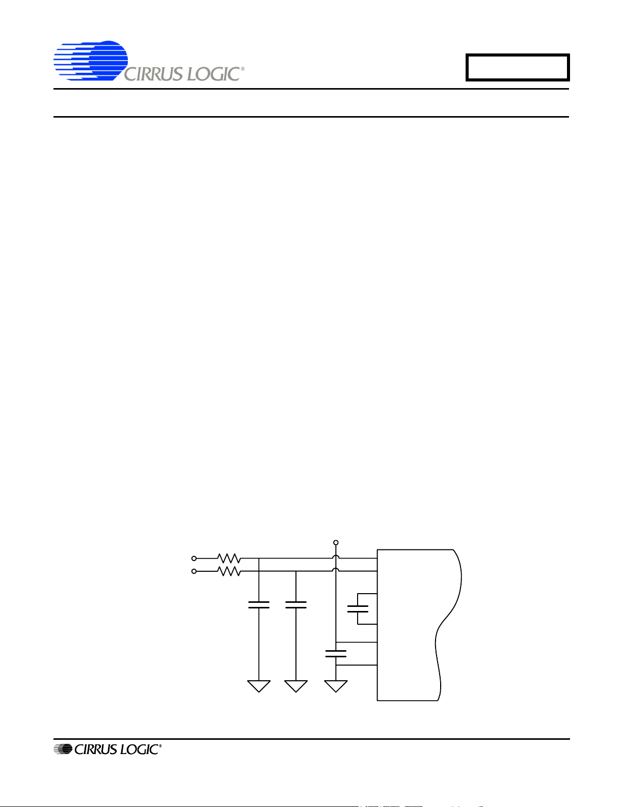
Consider the best possible PCB layout for the simple schematic shown in Figure 1 below.
V+
R1
AIN+
AIN-
R2
C1C2 C4
C3
1
2
5
6
7
8
AIN+
AIN-
CS5534
C1
C2
VA+
VA-
http://www.cirrus.com
Figure 1. Analog Input Circuit for a CS5534 ADC
Copyright © Cirrus Logic, Inc. 2006
(All Rights Reserved)
SEP ‘06
AN299REV1
Page 2
AN299
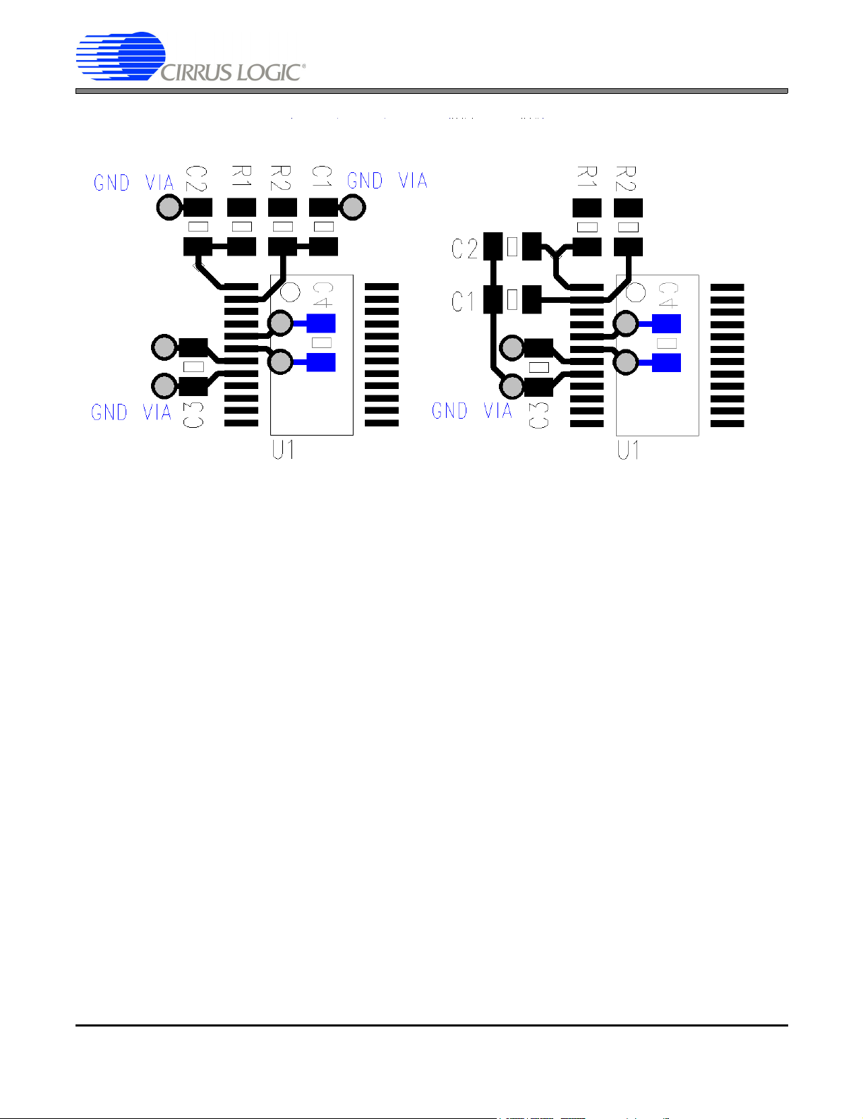
In this layout C1, C2, and C3 are connected to the ground plane with
three separate vias which may have noise voltage deltas among
them.
Figure 2. Preferred Layout for Minimizing Differential Noise from the Ground Plane
This layout is preferred because all three capacitors are connected to
the ground plane with one via so there can be no noise voltage delta
present.
As illustrated in Figure 2, if a high-speed signal return path or power supply return path flows through the ground
plane in such a way that introduces a noise voltage drop between the point where two capacitors, one on AIN+ and
one on AIN-, connect to the ground plane, a differential noise voltage will be inadvertently applied to the ADC input
through those capacitors.
This does not necessarily mean that, in order to avoid voltage drops across the plane, one should avoid using a
common ground plane for both digital and analog circuitry The debate about whether digital ground and analog
ground should be separated has gone on for years but one thing remains indisputable –
the digital ground (DGND)
pin and any other pin on the ADC that connects to analog ground must be tied together at the ADC via a very lowimpedance path. This includes bypass capacitors on the power pins and anti-aliasing and filter capacitors on the
AIN and VREF pins. If separate DGND and analog ground (AGND) planes are used, they must be tied together beneath the ADC. Also, take great care to prevent clock or high-speed digital signal traces from crossing splits in the
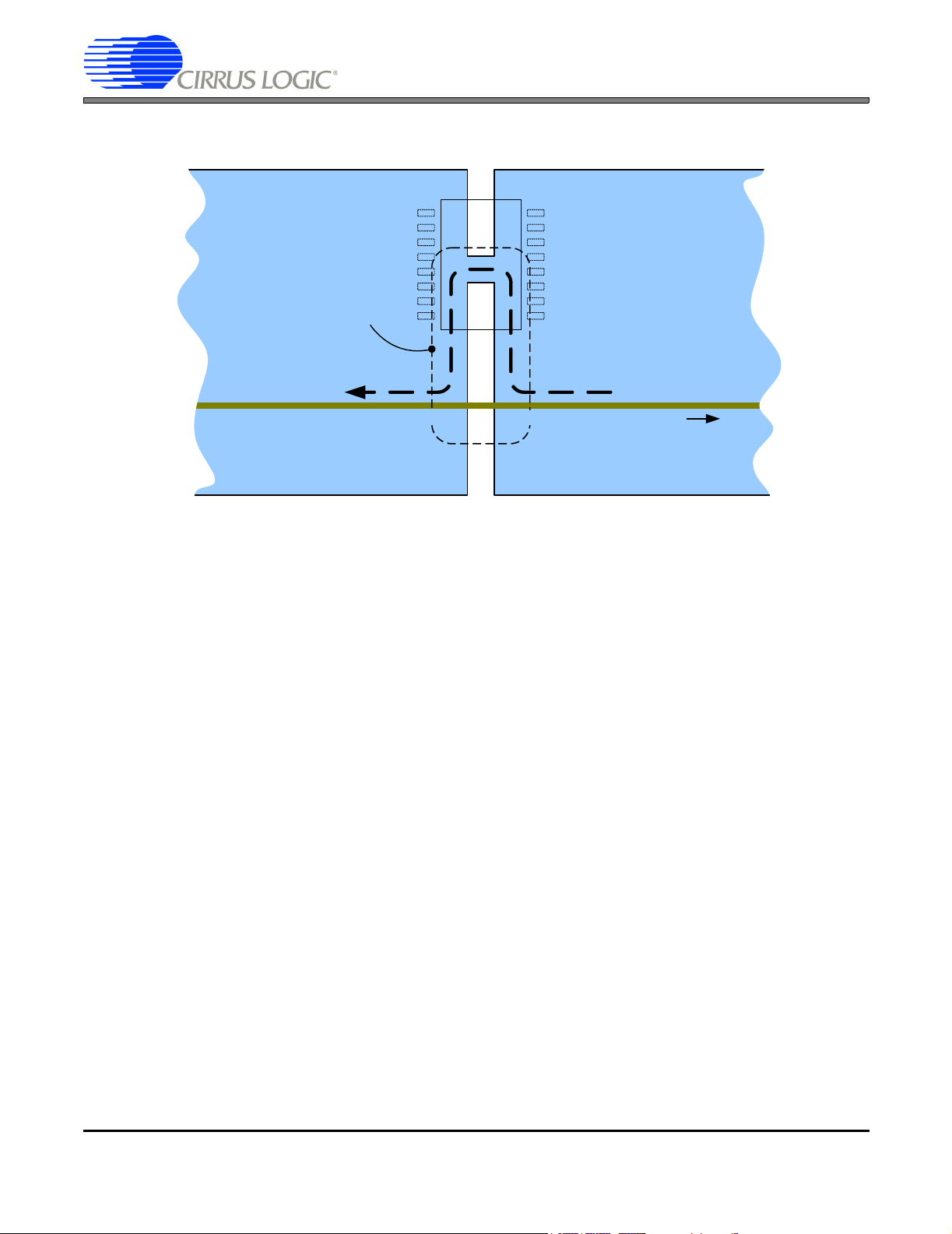
ground plane (or splits in an adjacent power plane). The problem with split or non-continuous planes is that highspeed return currents tend to return to the source in a path that is as close to the active trace as possible. However,
discontinuities in the adjacent ground or power plane force the currents to deviate from that path. This deviation results in “antenna” loops that radiate high-frequency energy as illustrated in Figure 3. Once these signals are radiated
it is very difficult to prevent them from being picked up by the sensitive analog inputs.
2 AN299REV1
Page 3
AN299
AGND
DGND
Loop antenna effect
radiates high-frequency
energy to other traces
Return Current
High-speed Digital Signal Trace On Adjacent Layer
Figure 3. Antenna Loop Caused by Ground or Power Plane Splits
It is important to note that the CS5531/2/3/4 devices do not have an AGND pin. The common-mode reference for
the analog inputs is VA- (the die substrate). In single-supply configurations it is important that VA- be connected to
the DGND pin through a low-impedance ground plane. In dual-supply configurations the bypass capacitors on VAand VA+ should be connected to the same ground as the DGND pin through low-ESR (effective series resistance)
bypass capacitors. The reason for this is that any noise differential between these pins will result in noise from the
digital core ground (DGND pin) getting into the internal analog circuitry through the level shifters and parasitic capacitance on the die. Also, any noise differential between the VA- pin and the anti-aliasing capacitors on the analog
inputs will result in common-mode noise being directly coupled to the inputs. Although the ADC has an excellent
common-mode rejection ratio (CMRR) at DC and low frequencies, the higher the frequency of the common mode
noise, the more likely it is that it will be sampled by the ADC and aliased into the pass band. This is especially true
of noise from switch-mode power supplies.
In general, the ADC should be located such that any heavy dynamic currents flowing in the ground plane are kept
away from the converter. This may require that the converter be located on the PCB as far from the power connections as possible. Furthermore, digital IO ports that leave the PCB should
currents these ports often must provide to charge parasitic capacitance on the cabling can create significant noise
differentials in the ground plane. If these guidelines are followed it may not be necessary to use separate analog
and digital ground planes. Therefore the problem of high-speed signals crossing splits in the plane is avoided.
not be located near the ADC. The transient
3. DECOUPLING (BYPASS) CAPACITORS
As noted previously, the choice and placement of capacitors for power supply decoupling is very important. The supply currents to mixed-signal devices are dynamic, not steady-state DC. If this dynamic current was supplied only by
a power source located away from the ADC, very large fluctuations in the voltages at the power pins of the device
would be seen as a result of the series impedances between the device and the power source. Therefore, capacitors
are required at the power pins of the device to act as a reservoir of charge for these dynamic currents. For this reason, these capacitors must be located as close as physically possible to the power pins in order to minimize the
series impedance between the power pins and the capacitors. The bypass capacitors for VA+ and VA- should be
between these power pins instead of from each pin to ground since they provide a reservoir of charge between the
AN299REV1 3
Page 4

AN299
power pins. The practice of placing the bypass capacitors on the opposite side of the circuit board and connecting
them to the power pins through vias should be avoided. The inductance of the via degrades the performance of the
capacitor significantly at high frequencies. Also, the capacitor should be placed between the ADC power pins and
the via(s) connecting to the power source. In other words, if the power pins are connected by vias to power or ground
planes, the capacitor should be between the power pins and the vias as illustrated by C3 in Figure 2.
It should also be noted that placement of C4, the 22 nF low-pass filter capacitor, is very important. In Figure 2 this
component is placed on the opposite side of the PCB and connected with vias. This is acceptable and preferred over
crowding the top side of the PCB with the VA+ bypass capacitor. In fact, traces to the C2 pin and the VA+ pin should
be kept away from each other to avoid leakage currents in high-humidity conditions.
It can be advantageous to have some impedance between the power pin bypass capacitors and the power source.
For example, when using the same power source for VA+ and VD+, it is recommended that a 10-ohm resistor is
placed between the VD+ pin and the power source. This is possible with CS553x devices because the VD+ pin requires very little average current and therefore only a small voltage drop occurs. Since the bypass capacitor on the
VD+ pin has a much lower source impedance than the 10-ohm resistor to the power source, the dynamic current
required by VD+ comes almost exclusively from the capacitor. This prevents digital noise from the VD+ pin from
being introduced on the VA+ pin. The same applies for VD- and VA- in bipolar power supply configurations.
The bypass capacitor also has a second purpose – to act as a power supply noise filter device. All power sources
contribute some amount of noise. It is very important to eliminate as much noise as possible from the VA+ and VAsupplies. One of the surest ways to degrade the performance of a high-resolution ADC is by powering it with a noisy
power source. Like CMRR, the power supply rejection ratio (PSRR) is good at low frequencies such as 50 or 60 Hz.
However, the PSRR decreases as the frequency increases. The higher the noise frequency, the more likely it is that
it will degrade the performance of the ADC. Therefore, it is wise to provide some means of filtering as much noise
as possible from the power source at the VA+ and VA- pins. One approach is to use inductors or ferrite beads to
introduce an impedance at higher frequencies only. However, care should be taken when using inductors in series
with the power source because, in conjunction with the bypass capacitors, they can resonate. This will result in a
“ringing” effect whenever a transient edge excites the LC circuit at its resonate frequency. This can be minimized by
including a small series resistance to damp the resonance of the LC circuit by lowering its Q factor. Often the resistance of the coil is adequate if the value of the inductance is sufficiently high.
If they are carefully chosen, ferrite beads can also be an effective means of reducing power supply noise. Unlike an
inductor, ferrite beads dissipate high-frequency energy rather than simply introducing a high impedance to it. Ferrite
beads will not resonate with the bypass capacitors. While a ferrite bead does have inductance, it can be thought of
as a frequency-dependent resistor and therefore has a very low Q factor. In selecting a ferrite bead to filter the power
supply, several parameters should be considered. First, the DC bias current characteristics must be determined.
Ferrite beads have a current rating which determines when the bead saturates. When a ferrite bead saturates, its
impedance drops off rapidly causing it to be ineffective at reducing high-frequency noise. Saturation is partially a
factor of the physical size of the bead. therefore, a larger ferrite bead may be more effective with higher currents.
The second characteristic that must be considered in selecting a ferrite bead is its effective frequency range. This
is determined by the composition of the ferrite alloy. For power supply filtering, the lowest-frequency compositions
should be the most effective. For example, the Fair-Rite
of 28 ohms at 1 MHz (see Figure 4). Many beads, especially surface mount beads, offer very little if any impedance
at this low frequency. Since much of switch-mode power supply harmonics will be in this frequency range, this component would be an effective means of attenuating much of that noise. This impedance, in combination with the low
impedance of an X7R ceramic capacitor will attenuate a large portion of the power supply noise with almost no DC
voltage drop. In a bipolar supply configuration, these capacitors should be between each supply pin and ground as
well as the capacitor from VA+ to VA- as mentioned earlier.
4 AN299REV1
®
P/N 2773021447 surface mount bead has an impedance
Page 5
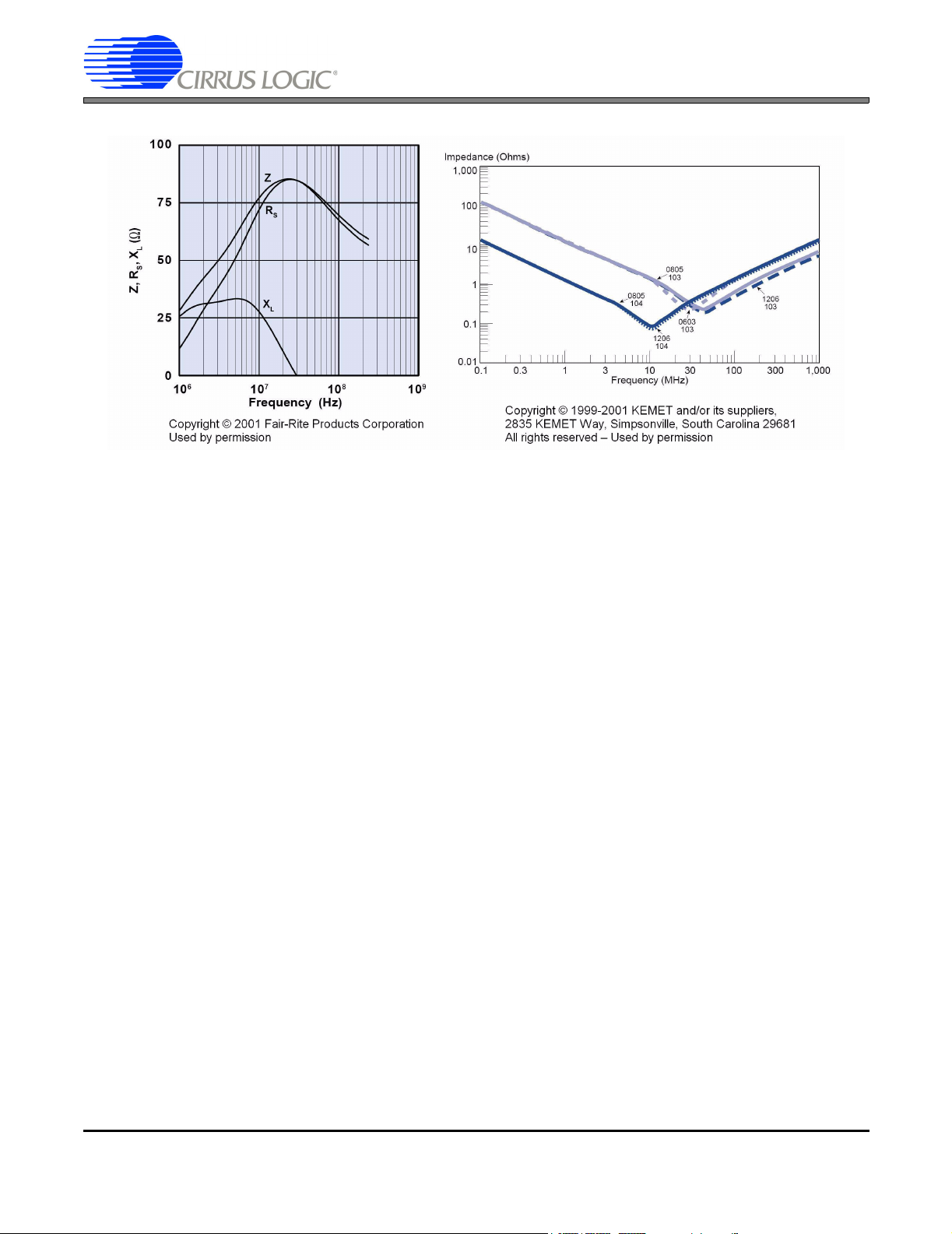
Figure 4. Ferrite Bead and X7R Ceramic Capacitor Impedance vs. Frequency
4. CONTROLLING DIGITAL SIGNAL NOISE
AN299
The ADC is a mixed-signal device and has digital as well as analog pins. Therefore, in most applications, there are
relatively high-energy digital signals in close proximity to very low-level analog signals - especially near the ADC
itself. Thus, great caution should be used to assure that the digital signals do not corrupt the low-level analog signals.
Two methods that have already been mentioned should be used –
the power or ground planes and avoiding locating digital ports that leave the board near the ADC.
Whether a crystal is used with the internal crystal oscillator or an external oscillator is used, the routing of the clock
traces to the ADC should be carefully placed. Again, avoid allowing the clock signals to cross a split in the power
and ground planes and route the clock as far from AIN and VREF signals as possible.
External clock oscillators and microcontroller or microprocessor serial bus signals often have much faster edges
than are required by the ADC. These fast edges along with circuit board parasitic capacitance and inductance often
create reflections and high-energy harmonics into the hundreds of megahertz. One effective way to minimize these
reflections and harmonics is to put a damping resistor in series with the trace as close to the source pin as possible.
For example, the SCLK and SDI signals from a microprocessor or microcontroller could have 20- to 50-ohm series
resistors at the microprocessor pins and the SDO signal could likewise have a 20- to 50-ohm resistor at the ADC
SDO pin. The actual value of the resistor will depend on the board parasitics and trace lengths and could be determined by simulation software (such as HyperLynx
after the board is built by observing the signal with a low capacitance oscilloscope probe. Using the probe, the smallest resistor value that eliminates overshoot and undershoot and other reflection induced artifacts should be used.
Obviously too large a resistor value will result in excessive slewing of the digital signals and may compromise the
noise immunity of the digital interface. Generally the resistor value should be 50 ohms or less.
®
from Mentor Graphics®) or it could be determined empirically
avoiding high-speed signals crossing splits in
5. OPTIMIZING THE INPUT SPAN
The CS5531/32/33/34 delta-sigma converters have a built-in digital filter and calibration engine. The delta-sigma
modulator generates a single-bit bitstream of 307,200 bits per second (assuming a 4.9152 MHz crystal or oscillator
and FRS = 0) which is the input to the digital filter. From this bitstream the digital filter creates a parallel digital word
representative of the analog input voltage. The calibration engine takes this digital value (which has more resolution
than the output word), adds the offset correction from that channel's offset calibration register, and then multiplies
that result by the contents of the gain calibration register for that channel. This result is then truncated to
AN299REV1 5
Page 6

AN299
16 (CS5531/3) or 24 (CS5532/4) bits and placed in the output register. At reset the value in all of the offset registers
is zero (0x00000000) and the gain correction registers contain a gain multiplier of one (0x01000000). If the offset
and gain corrections are not required by an application, as is often the case in ratiometric applications, the gain calibration register can be used to change the full-scale input span of the ADC. For example, if the channel setup is
programmed for a gain of 64x in unipolar mode, the full-scale input span with a 2.5 V DC reference (VRS = 1) or 5 V
DC reference (VRS = 0) would be 39.0625 mV. However, if it is desired to have the full-scale range be 10 mV, this
could be achieved by writing a value of 3.90625 (0x03E80000) into the gain calibration register for that channel.
Since the internal resolution of the filter's output is several bits greater than the output word resolution, multiplying
by 3.90625 results in almost two bits of that internal resolution being utilized in the output that would have otherwise
been truncated. This in itself does not improve the noise-free resolution of the output, but with adequate software
averaging of this output, additional noise-free bits are possible as long as the noise distribution is Gaussian. It should
be pointed out that if this method is used, the offset register should be zero. Otherwise an offset calibration should
be performed after the gain register is written because the offset value will also be multiplied by the gain register
value.
6. DC MEASUREMENT AVERAGING
The above section referred to averaging the ADC readings in software in order to obtain additional noise-free bits
of resolution. In DC measurement, where the input seldom changes, this can be a simple average. Otherwise a running average or a more adaptive, weighted average that detects changes in the DC input above a certain threshold
can be used. Which method is used and what sample rate is used will depend on the system requirements for the
DC reading. How much latency can be tolerated between an input change and the completely settled result needs
to be determined before an averaging algorithm is chosen. The purpose of this explanation is simply to suggest a
few methods that could be implemented, especially when noise-free resolution is the main concern.
Before a software averaging algorithm is chosen, the sample rate for the converter should be selected. For measuring a steady-state DC input, the advantages of using a low sample rate such as 7.5 Sps should be noted. To remove
as much of the noise as possible, lower sample rates take better advantage of the on-chip digital filter. However,
this conversion rate is based on the CS553x continuous conversion mode where complete settling only occurs after
four conversions. If the input multiplexer is used, single conversion mode is recommended because each conversion
is fully settled (in essence the part converts the input four times before giving an output word). The slowest output
rate in this case is approximately 1.8 Sps. Therefore in many applications where the inputs are being multiplexed it
may be desirable to use a higher conversion rate and average each input in software to remove some of the noise.
There is an advantage in using conversion rates of 60 Sps (50 Sps when FRS = 1) or lower because power line
frequency rejection is excellent at these rates due to a notch in the sinc3 filter at this frequency.
Once the conversion rate is determined, a software algorithm for averaging the readings for each channel to remove
more noise may be useful. A
then divided by eight giving each conversion equal weight. This average fully settles in eight conversions since all
conversion results before the last eight are discarded.
ing being a fractional part of the averaged result. For example, if the new reading is multiplied by 0.125 and then
added to the previous average multiplied by 0.875 then the new reading becomes 1/8 of the average. In this algorithm the most-recent value has the highest weight with older conversions diminishing in weight exponentially. However, this exponential averaging has the highest latency because it takes many conversions for a single reading to
be completely flushed from the average, especially when a step change occurs on the input. In fact, a full-scale
change on a 24-bit converter would take 83 conversions for the average to settle to 16 bits of accuracy. Another
algorithm is the
difference between it and the previous average. Here a threshold needs to be determined that indicates that a step
change has occurred on the input. This threshold should be above normal peak-to-peak system noise in order that
noise below the threshold can be averaged out by the normal exponential average. However, if the new reading is
beyond the normal peak-to-peak noise threshold, the new reading supersedes the average so that the step is made
in a single conversion. This algorithm has numerous possibilities if multiple thresholds are specified with each step
adaptive exponential average. In this case, the weight of the new ADC reading depends on the
simple running average of eight is where only the last eight conversions are added
Simple exponential averaging is defined as each new read-
6 AN299REV1
Page 7
AN299
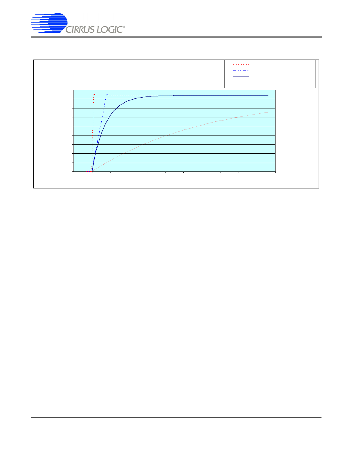
magnitude resulting in higher weights for the new reading. See Figure 5 to compare the step responses of these
algorithms.
Adaptive Avg. of 8
Running Avg. of 8
Exponential Avg. of 8
Exp Avg. of 64
18000000
16000000
14000000
12000000
10000000
8000000
Output Code
6000000
4000000
2000000
Averaging Algorithm Responses
0
-10 0 10 20 30 40 50 60 70 80 90 100
Number of conversions
Figure 5. Algorithm Step Response Comparison
Figures 5a, 5b, 5c, and 5d illustrate the typical peak-to-peak noise performance of a CS5532AS with a gain of 64
and word rate of 60 Sps. Figure 5a shows the noise performance without software filtering and the other three plots
illustrate the effects of applying different software filtering algorithms. Without any software filtering, the peak-topeak noise is 64 codes or 6 bits, which is consistent with the data sheet’s specification of 18 noise-free bits. With
the simple running average of 8 algorithm, approximately one more bit of noise-free performance can be gained
(peak-to-peak noise of 35 codes), while the simple exponential average of 8 gives slightly better improvement (27
codes peak-to-peak). The simple exponential average of 64 results in approximately 8 codes peak-to-peak or a
noise-free resolution improvement of 3 bits.
AN299REV1 7
Page 8

AN299
50
40
30
20
10
0
-10
-20
Normal ized Outp ut Code ( lsb)
-30
-40
-50
0 200 400 600 800 1000
Sample s
Figure 5a. Noise Performance – No Software Filtering
50
40
30
20
10
0
-10
-20
Normal ized Outp ut Code ( lsb)
-30
-40
-50
0 200 400 600 800 1000
Sample s
Figure 5b. Noise Performance – Simple Running Average of 8
50
45
40
35
30
25
20
15
10
5
0
80
70
60
50
40
30
20
10
0
Mean -2.98E-13
Max 31.88
Min -32.12
P-P 64.00
StdDev 10.90
6050403020100-10-20-30-40-50-60
Mean -6.28E-02
Max 18.13
Min -17.37
P-P 35.50
StdDev 6.23
6050403020100-10-20-30-40-50-60
50
40
30
20
10
0
-10
-20
Normal ized Outp ut Code ( lsb)
-30
-40
-50
0 200 400 600 800 1000
Sample s
Figure 5c. Noise Performance – Simple Exponential Average of 8
50
40
30
20
10
0
-10
-20
Normal ized Outp ut Code ( lsb)
-30
-40
-50
0 200 400 600 800 1000
Sample s
Figure 5d. Noise Performance – Simple Exponential Average of 64
90
80
70
60
50
40
30
20
10
0
200
180
160
140
120
100
80
60
40
20
0
Mean -9.44E-02
Max 13.49
Min -13.58
P-P 27.07
StdDev 4.91
6050403020100-10-20-30-40-50-60
Mean -1.35E-01
Max 3.85
Min -4.25
P-P 8.10
StdDev 1.96
6050403020100-10-20-30-40-50-60
8 AN299REV1
Page 9

AN299
w
In most applications the simple exponential average of 64 would result in excessive output settling latency, so an
adaptive algorithm could be used to allow a quicker response to step changes in the input. The following code segment uses two thresholds to accomplish a quick response while improving noise-free performance by 3 bits for a
steady state input.
hile(1)
{
NewValue = ReadADC();
Difference = abs ( NewValue – Average );
if ( Difference > 256 ) /* No software average for large steps */
Average = NewValue;
else if ( Difference > 64 ) /* Exponential average of 8 for medium step size */
Average = Average * 0.875 + NewValue * 0.125;
else /* Exp. ave. of 64 for steady state noise reduction */
Average = Average * 0.984375 + NewValue * 0.015625;
/* Scale the value for readout after averaging */
DisplayValue = ScaleValue( Average );
UpdateDisplay( DisplayValue );
}
Figure 6. Adaptive Algorithm Code Example
In this code, if any step in ADC output over 8 bits is detected, the average is updated to the new value without any
software filtering. If continuous conversion mode is used there will still be a four-conversion latency. However, this
will minimize overshoot and if a faster word rate is used, the latency should be acceptable for most applications. If
the step size is between 64 and 256, a simple exponential average of 8 is used allowing reasonably fast settling as
the final value is approached. Once the new value is within 64 bits of the average value the algorithm switches to a
simple exponential average of 64. As long as the input remains within a ±64 LSB range, the simple average of 64
is maintained, resulting in 3 additional noise-free bits of performance for steady-state inputs. For slower microcontrollers which do not have floating point units, left and right shifts on integer values and subtraction and addition can
be used as long as the filter coefficients are powers of two.
7. CONCLUSION
As this application note explains, there are many factors that determine the success of a high-resolution ADC implementation. The Cirrus CS5531/32/33/34 family of converters are some of the quietest converters on the market
and if careful mixed-signal design practices are observed, incredibly accurate high-resolution measurements of very
low-level DC signals can be achieved.
As always, Cirrus Logic applications support offers schematic and PCB layout review to our customers. In many
cases less-than-optimum designs or layout errors can be corrected before the PCB is produced.
AN299REV1 9
Page 10

8. REVISION HISTORY
Release Date Changes
REV1 SEP 2006 Initial Release
AN299
Contacting Cirrus Logic Support
For all product questions and inquiries, contact a Cirrus Logic Sales Representative.
To find the one nearest to you, go to http://www.cirrus.com
IMPORTANT NOTICE
Cirrus Logic, Inc. and its subsidiaries ("Cirrus") believe that the information contained in this document is accurate and reliable. However, the information is subject
to change without notice and is provided "AS IS" without warranty of any kind (express or implied). Customers are advised to obtain the latest version of relevant
information to verify, before placing orders, that information being relied on is current and complete. All products are sold subject to the terms and conditions of sale
supplied at the time of order acknowledgment, including those pertaining to warranty, indemnification, and limitation of liability. No responsibility is assumed by Cirrus
for the use of this information, including use of this information as the basis for manufacture or sale of any items, or for infringement of patents or other rights of third
parties. This document is the property of Cirrus and by furnishing this information, Cirrus grants no license, express or implied under any patents, mask work rights,
copyrights, trademarks, trade secrets or other intellectual property rights. Cirrus owns the copyrights associated with the information contained herein and gives consent for copies to be made of the information only for use within your organization with respect to Cirrus integrated circuits or other products of Cirrus. This consent
does not extend to other copying such as copying for general distribution, advertising or promotional purposes, or for creating any work for resale.
CERTAIN APPLICATIONS USING SEMICONDUCTOR PRODUCTS MAY INVOLVE POTENTIAL RISKS OF DEATH, PERSONAL INJURY, OR SEVERE PROPERTY OR ENVIRONMENTAL DAMAGE (“CRITICAL APPLICATIONS”). CIRRUS PRODUCTS ARE NOT DESIGNED, AUTHORIZED OR WARRANTED FOR USE
IN AIRCRAFT SYSTEMS, MILITARY APPLICATIONS, PRODUCTS SURGICALLY IMPLANTED INTO THE BODY, AUTOMOTIVE SAFETY OR SECURITY DEVICES, LIFE SUPPORT PRODUCTS OR OTHER CRITICAL APPLICATIONS. INCLUSION OF CIRRUS PRODUCTS IN SUCH APPLICATIONS IS UNDERSTOOD
TO BE FULLY AT THE CUSTOMER’S RISK AND CIRRUS DISCLAIMS AND MAKES NO WARRANTY, EXPRESS, STATUTORY OR IMPLIED, INCLUDING THE
IMPLIED WARRANTIES OF MERCHANTABILITY AND FITNESS FOR PARTICULAR PURPOSE, WITH REGARD TO ANY CIRRUS PRODUCT THAT IS USED
IN SUCH A MANNER. IF THE CUSTOMER OR CUSTOMER’S CUSTOMER USES OR PERMITS THE USE OF CIRRUS PRODUCTS IN CRITICAL APPLICATIONS, CUSTOMER AGREES, BY SUCH USE, TO FULLY INDEMNIFY CIRRUS, ITS OFFICERS, DIRECTORS, EMPLOYEES, DISTRIBUTORS AND OTHER
AGENTS FROM ANY AND ALL LIABILITY, INCLUDING ATTORNEYS’ FEES AND COSTS, THAT MAY RESULT FROM OR ARISE IN CONNECTION WITH
THESE USES.
Cirrus Logic, Cirrus, and the Cirrus Logic logo designs are trademarks of Cirrus Logic, Inc. All other brand and product names in this document may be trademarks
or service marks of their respective owners.
Mentor Graphics and HyperLynx are registered trademarks of Mentor Graphics.
10 AN299REV1
 Loading...