

Page 1
AN285
CS5333 to CS5343/4 Transition
1. INTRODUCTION
The CS5333 and CS5343/4 are complete stereo analog-to-digital converters for digital audio systems. These converters perform sampling, analog-to-digital conversion and anti-alias filtering, generating 24-bit values for both left
and right channels. These small, low-power converters are ideal for systems r equiring wide dynamic ran ge and low
noise such as set-top boxes, A/V receivers, DVD-karaoke players, DVD recorders, and automotive applications.
The CS5333 is no longer recommended for new designs, and the CS5343/4 is the suggested replacement.
This application note identifies the implementation differences between these two devices, including:
• Key specifications
• Pinout differences
• Startup mode selections
• System clocking
• Input filter topology
• Reference voltage
The CS5333 and CS5343/4 datasheets contain detailed information regarding device specifications, performance
and ordering information. Please reference the CS5333 and CS5343/4 datasheets while reading this document.
2. KEY SPECIFICATIONS
Table 1 shows a comparison of the key specifications of these two device families, and Table 2 shows the pin com-
parison between the CS5333 and the CS5343/4. Although these two devices are not pin compatible, they are very
similar in terms of overall functionality and feature set.
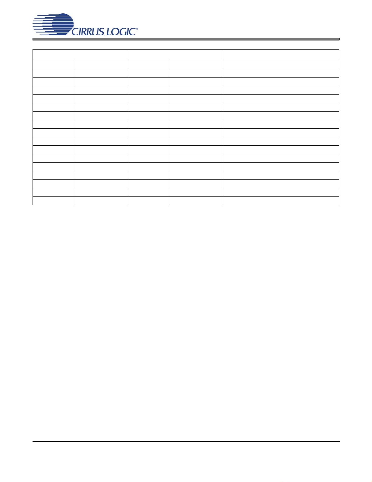
Parameter CS5333 CS5343/4 Units
Conversion 24 24 Bits
Dynamic Range (A-Weighted) 98 98 dB
THD+N -88 -90 dB
Analog Core Power Supply (VA) +1.8 to +3.3 +3.3 to 5 V
Digital Core Power Supply (VD) Powered from VA Powered from VA V
Digital Interface Power Supply (VL) +1.8 to +3.3 Powered from VA V
Typical Power ConsumptionAll supplies = +3.3 V 36 50 mW
Maximum Sample Rate 100 108 kHz
Package 16-pin TSSOP 10-pin TSSOP
T able 1. Comparison of Key Specifications
http://www.cirrus.com
Copyright © Cirrus Logic, Inc. 2005
(All Rights Reserved)
SEPTEMBER '05
AN285REV1
Page 2
CS5333 CS5343/4 Description
Pin Number Pin Name Pin Number Pin Name
1 VL - - Logic Power
2 MCLK 4 MCLK Master Clock
3 SCLK 2 SCLK Serial Clock
4 SDATA 1 SDOUT Serial Data
5 VA 10 V A Power
6 GND 9 GND Ground Reference
7 LRCK 3 LRCK Left/Right Clock
8 DIV - - Speed Mode Select/MCLK Divider
9 DIF - - Digital Interface Format
10 TST - - Test Pin
1 1 FILT+ 5 FILT+ Full-Scale Voltage Reference
12 REF_GND - - Ground Reference
13 AINR 8 AINR Right Channel Analog Input
14 AINL 6 AINL Left Channel Analog Input
15 VQ 7 VQ Quiescent Voltage Reference
16 RST - - Reset
T able 2. Pin Comp atibility between the CS5333 and CS5343/4
AN285
2 AN285REV1
Page 3
AN285
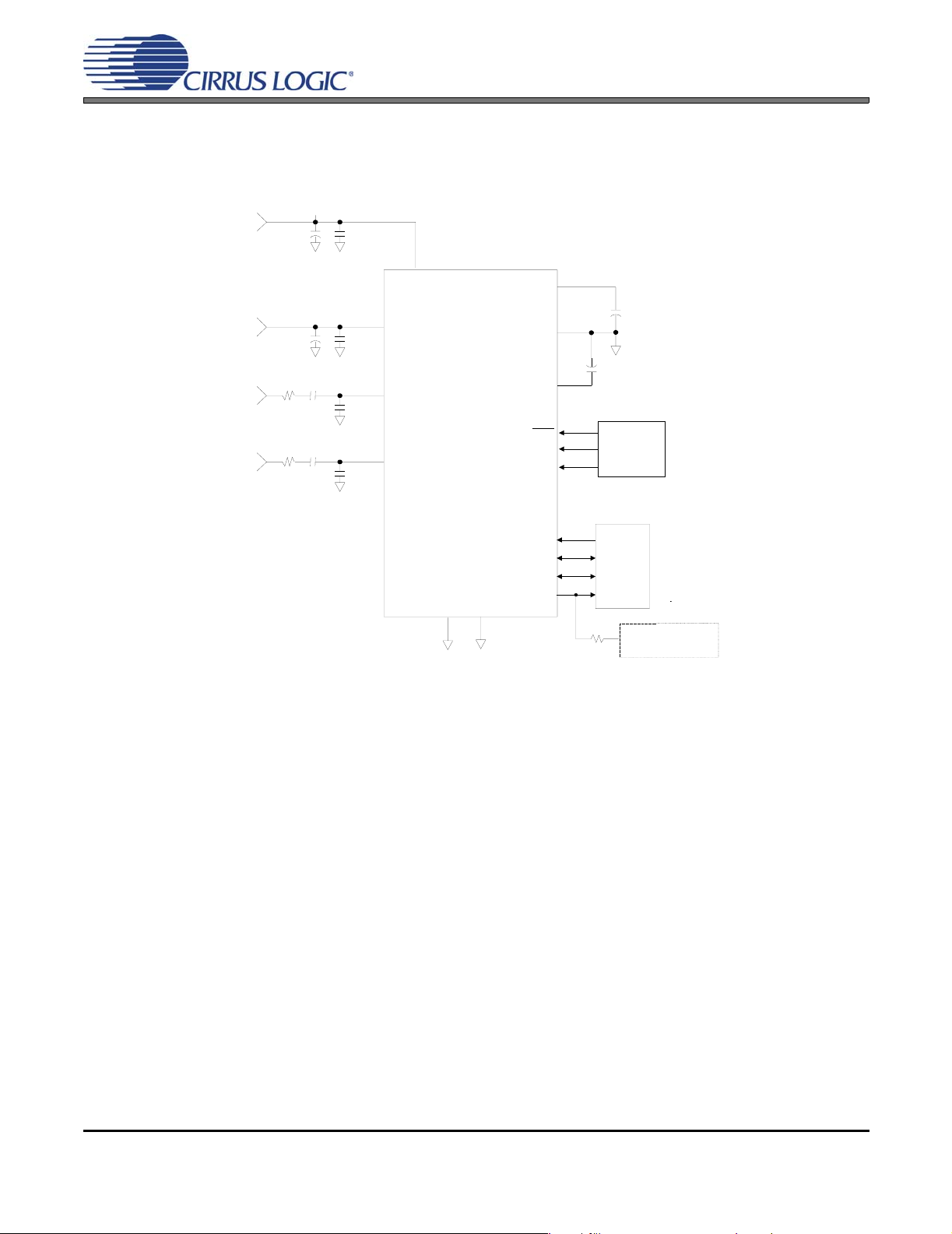
3. TYPICAL CONNECTION DIAGRAMS
Figures 1 and 2 are the typical connection diagrams for the CS5333 and the CS5343/4 respectively. These dia-
grams demonstrate optimal power arrangements and the options available with pull-up or pull-down resistors on various I/O pins for each device.
1.8 to 3.3 V
Supply
1.8 to 3.3 V
Supply
* All capacitors located
on the analog input lines
should be of the type
COG or equivalent.
**Optional if analog input
circuit is biased within
±5% of CS5333 nominal
bias voltage
1.0 µF
1.0 µF
Ω
150
Ω
150
+
+
**
**
0.47 µF
0.47 µF
0.1 µF
1
0.1 µF
14
0.01 µF
*
13
0.01 µF
*
VL
AINL
AINR
5
VA
CS5333
GND6TST
10
FILT+
REF_GND
VQ
RST
DIF
DIV
MCLK
LRCK
SCLK
SDATA
11
12
15
16
9
8
2
7
3
4
1.0 µF
+
1.0 µF
Configuration
Digital
Audio
Source
47k
Ω
+
Mode
Connect to:
• VL for Master Mode
• GND for Slave Mode
Figure 1. CS5333 Typical Connection Diagram
AN285REV1 3
Page 4

AN285
+
µ
1
F
1µ
F
+
Analog Input
Circuitry
Figure 4
0.1µF
0.1µF
FILT+
GND
VQ
AINL
AINR
VA
CS5343/4
A/D Converter
+
1µF
SDOUT
SCLK
LRCK
MCLK
3.3 V to 5 V
0.1µF
VA or GND
1
Ω10k
Audio Data
Processor
VA
.
2
k
Ω10
2
Ω10k
Timing Logic
and Clock
1.
Pull-up to VA for Master Mode
Pull-down to GND for Slave Mode
2.
Optional pull-up resistor for configuring
clocks in Master Mode as described in
Sections 5.2 and 6.2
4. POWER
4.1 CS5333 Power
The CS5333 receives power to the analog and digital cores through the VA supply pin, while VL powers the
digital interface logic. Both VA and VL on the CS5333 can accept power ra nging from +1.7 V to +3.6 V. The
full-scale reference voltage scales with VA such that nominal full-scale voltage is VA/3.6 Vrms. VL determines the digital interface voltage to within the specifications listed under “Digital Characteristics” in the
CS5333 datasheet.
4.2 CS5343/4 Power
The CS5343/4 features a single supply pin, VA, which powe rs the analog and digital cores as well as the
digital interface logic. With a range from +3.13 to +5.25 V, VA determines the no minal full-scale input voltage
according to 0.56xVA Vpp. Additionally, VA also determines the digital interf ace voltage as described further
under “Digital Characteristics” in the CS534 3/ 4 da ta sh ee t.
Figure 2. CS5343/4 Typical Connection Diagram
4 AN285REV1
Page 5

5. MODE SELECTIONS: MASTER/SLAVE & SPEED MODES
5.1 CS5333 Mode Selections
5.1.1 Master/Slave Mode Selection
The CS5333 operates in either Master Mode or Slave Mode depending on the pull-up or pull-down resistor
on the SDATA pin. A 47 kΩ pull-up resistor between SDATA and VL selects Master Mode while a 47 kΩ
resistor between SDATA and GND will select Slave Mode.
5.1.2 Speed Mode Selection
The CS5333 features a DIV pin which allows the user to configure speed in Master Mode. In Master Mode,
the user can tie DIV high (VL) to select Base-Rate mode or low (GND) to select High-Rate mode. In Slave
Mode, the CS5333 auto-detects speed mode and the DIV pin enables an MCLK divide-by-two function
when set high.
5.2 CS5343/4 Mode Selections
5.2.1 Master/Slave Mode Selection
The CS5343/4 enters Master Mode when a 10 kΩ pull-up resistor is prese nt between SDOUT and the VA
supply. Conversely, Slave Mode is selected via a pull-down resistor between SDOUT and GND.
AN285
5.2.2 Speed Mode Selection
Similar to the CS5333, the CS5343/4 auto-detects Speed Mode when operating as a slave. In Master
Mode, an internal 100 kΩ pull-down resistor on the LRCK pin will set the device for Single-Speed Mode
by default. An external 10 kΩ pull-up resistor from the LRCK pin to VA will over-ride the default setting
and select for Double-Speed Mode.
Unlike the CS5333, the CS5343/4 features additional auto-detect circuitry to automatically enable an
MCLK divide-by-two function.
AN285REV1 5
Page 6

6. SYSTEM CLOCKING
6.1 CS5333 Clock Options
The CS5333 supports an MCLK/LRCK ratio of 256x, 384x, 512x, and 768x in Base-Rate Mode, and 128x,
192x, 256x, and 384x in High-Rate Mode. However, in Master Mode, MCLK/LRCK ratios of 384x, 768x, and
192x are not accessible. Table 3 shows the available MCLK/LRCK ratios in each mode of oper ation for the
CS5333.
Furthermore, the CS5333 supports sample rates from 2 to 50 kHz in Base-Rate Mode an d 50 to 100 kHz in
High-Rate Mode.
Device Master/Slave Speed Supported MCLK/LRCK Ratio
CS5333
6.2 CS5343/4 Clock Options
Table 4 shows the MCLK/LRCK ratios the CS5343/4 can support in the various modes of operation.
Master
Slave
Table 3. CS5333 Supported MCLK/LRCK Ratios
Base-Rate 256x
High-Rate 128x
Base-Rate 256x, 384x, 512x, 768x, 1024x
High-Rate 128x, 192x, 256x, 384x
AN285
In Slave Mode, the CS5343/4 supports MCLK/LRCK ratios of 128x, 192x, 256x and 384x when running in
either Single-Speed or Double-Speed. Also in Slave Mode, the CS5343/4 sample-rate can range continuously from 4 to 54 kHz in Single-Speed Mode or 86 - 108 kHz in Double-Speed Mode.
In Master Mode, the CS5343/4 defaults to an MCLK/LRCK ratio of 256x due to the presence of a 100 kΩ
internal pull-down resistor between the SCLK pin and GND. An external 10 kΩ pull-up resistor from the
SCLK pin to VA will configure the device to output an LRCK corresponding to an MCLK/LRCK ratio of 384x,
depending on MCLK frequency. With the correct MCLK frequen cy and clock divid er settings, the CS5343/4
sample-rate can range continuously from 4 to 54 kHz in Single-Speed Mode or 50 to 108 kHz in DoubleSpeed Mode.
Device Master/Slave Speed Supported MCLK/LRCK Ratio
Master
CS5343/4
Slave
Table 4. CS5343/4 Supported MCLK/LRCK Ratios
Single-Speed 256x, 384x
Double-Speed 256x, 384x
Single-Speed 128x, 192x, 256x, 384x
Double-Speed 128x, 192x, 256x, 384x
6 AN285REV1
Page 7
7. INPUT FILTER TOPOLOGY
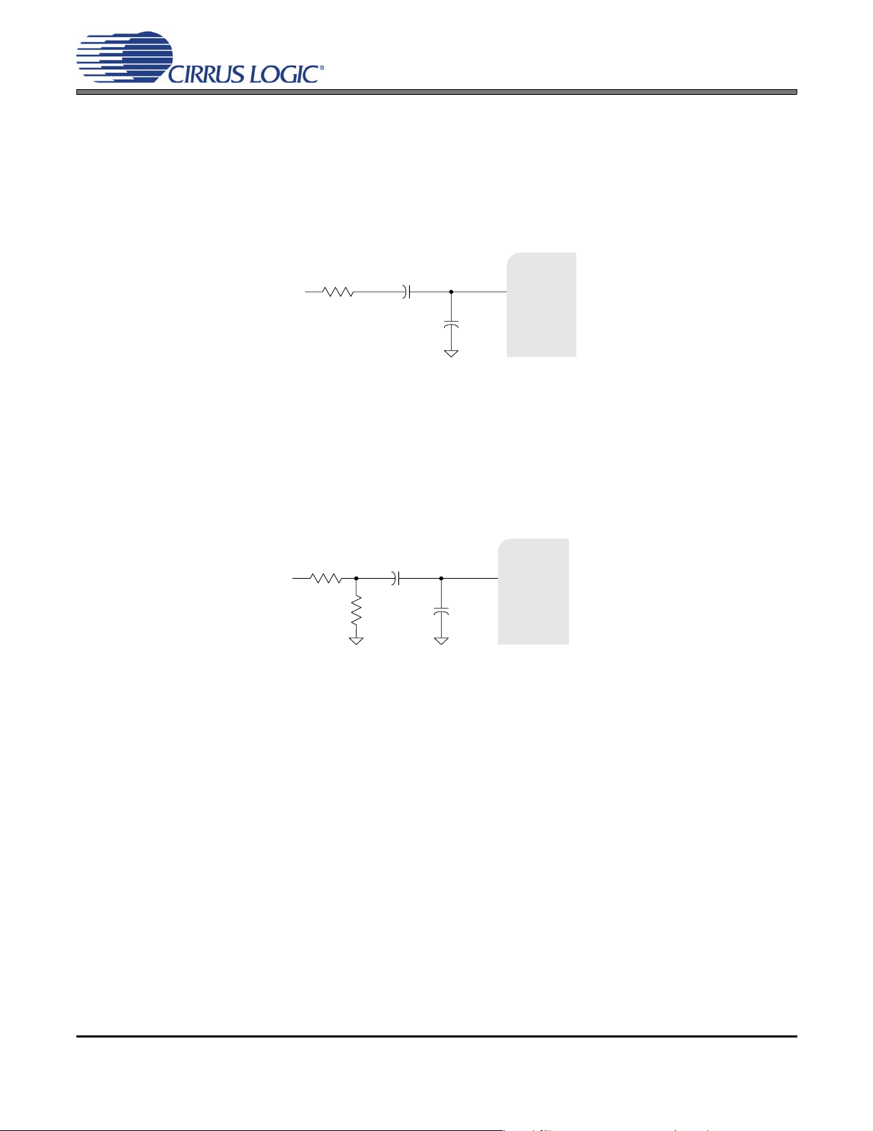
7.1 CS5333 Input Filter
Figure 3 shows the recommended input circuit for the CS5333. The CS5333 contains an internal continu-
ous-time buffer. The external circuit provides filtering of high-frequency noise via the single-pole RC filter.
The CS5333 will self-bias the input to the reference voltage (half of VA). If the incoming signal is not DC
biased to within 5% of this value, then the series DC-blocking capacitor is necessary.
AN285
150 Ω
0.47µF
Figure 3. CS5333 Input Circuit
7.2 CS5343/4 Input Filter
7.2.1 CS5343/4 Recommended Circuit
Figure 4 shows the typical analog input network for the CS5343/4. The componen t values shown are not
mandatory, but this particular c ircuit has four features that make it ideal for most applications, as discussed below. Please see the CS534/4 datasheet for more information regarding component selection.
5k
Ω
5k
Ω
Figure 4. CS5343/4 Typical Input Circuit
1µF
270 pF
CS5333
AIN
0.01µF
C0G
CS5343/4
AIN
C0G
• Input Impedance: This circuit’s input impedance as seen from the an alog source looking into the circuit
is 10 kΩ, which means this circuit will provide the ideal interface to most consumer equipment.
• Attenuation: This circuit also attenuates the analog input signal by 6 dB. This further simplifies the interface between consumer equipment and the ADC because most consumer equipment generate 2
Vrms line voltage. The circuit in Figure 4 attenuates the incoming signal from 2 Vrms to 1 Vrms, which
is the full-scale input voltage of the CS5343/4 when VA = 5V.
• Source Impedance: The CS5343/4 achieves optimal analog performance wh en the source impedance
as seen from the ADC looking into this network remains at or below 2.5 kΩ. The ADC effectively “sees”
two 5 kΩ resistors in parallel, or 2.5 kΩ!
• Noise Rejection: Under typical conditions, the modulators in the ADC generate switching noise at
6.144 MHz, or half of the MCLK frequency. The single-pole RC filter formed by the shunt capacitor and
the input impedance of the device will provide approximately 20 dB of attenuation at the modulator
switching frequency. For this and other capacitors in the signal path, capacitors with C0G or other highquality dielectric will produce the best results.
AN285REV1 7
Page 8

AN285
7.2.2 CS5343/4 Full-Scale Voltage
The CS5333 full-scale input voltage is 0.78xVA Vpp whereas the CS5343/4 full-scale input voltage is
0.56xVA Vpp, a difference of nearly 3 dB. This means that without attenuation, a full-scale signal to the
CS5333 will over-range the CS5343/4. In migrating from the CS5333 to the CS5343/4, the input signal
should either be reduced by 3 dB at the source or resistor values should be chosen such that the
CS5343/4 input network provides 3 dB of attenuation. The following equation yields the attenuation (in
dB) of the input network where R1 represents the series resistor and R2 is the resistor to ground:
R2
⎛⎞
------------------- -
log×
20
⎝⎠
R1 R2+
8. REFERENCE VOLTAGES
The reference voltage pins have the same configuration and usage on the CS5343/4 as the CS5333. FILT+ on both
devices outputs the full-scale voltage reference (VA), while the VQ pin outputs the common-mode voltage (VAx0.5
for the CS5333; VAx0.44 for the CS5343/4). Neither FILT+ nor VQ on either device can source current without degrading the analog performance of the device.
8.1 Filter Capacitors
The filter capacitors on these pins provide rejection of po wer- supply noise and conse quently affect THD+N
performance. Both devices require 1 µF filter capacitors from the voltage refe rence pins to GND. Larger capacitors will improve low-frequency THD+N to within the limitations of the device. A small capacitor, such
as a 0.1 µF, placed close to the device will filter high-frequency noise.
8.2 Settling Time
Following initial power-up, the analog reference voltage requires time to settle before conversion can be
considered valid. Settling time of the reference voltage depends on the output impedance (R
value of the external capacitance (C
For the same value capacitors on the CS5333 and CS5343/4 voltage reference pins, the CS5343/4 will require shorter settling time than the CS5333 due to the hig her output impe dance of th e CS5333 FILT+. Typical output impedance of the CS5333 FILT+ is 250 kΩ whereas CS5343/4 typical FILT+ output impedance
is 220 kΩ. This means the CS5343/4 reference voltage will settle 12% faster than the CS5333 reference
voltage.
) according to the following equation (time given in seconds):
ext
SettlingTime s() 5 Rout Cext××=
9. DIGITAL INTERFACE FORMAT
Please see Application Note AN282 for a complete overview of the serial audio interface (SAI).
9.1 CS5333 Interface Format
The CS5333 features a DIF pin to select between I²S and LJ digital audio formats. I²S digital audio format
is selected when DIF is tied low at start-up whereas the CS5333 will output LJ audio data when DIF is tied
to VL at start-up.
9.2 CS5343/4 Interface Format
) and the
out
The CS5343/4 family of converters supports both I²S and LJ digital audio format. Specifically, the CS5343
will support only I²S digital audio format while the CS5344 will output only LJ audio data.
8 AN285REV1
Page 9

AN285
10.CONCLUSION
With special attention to power arrangements, mode and clocking configurations, analog input circuitry, and reference voltage filtering, the transition from CS5333 to CS5343/4 should be simple and seamless. Furthermore, the
CS5343/4 can improve system design by offering superior performance to the CS5333 while significantly reducing
board space.
11.REVISION HISTORY
Release Date Changes
A1 September 2005 Initial Advance Release.
Contacting Cirrus Logic Support
For all product questions and inquiries contact a Cirrus Logic Sales Representative.
To find the one nearest to you go to www.cirrus.com/corporate/contacts/sales.cfm
IMPORTANT NOTICE
Cirrus Logic, Inc. and its subsidiaries ("Cirrus") believe that the information contained in this document is accurate and reliable. However, the information is subject
to change without not ice and is pr ovided "AS IS" witho ut warr anty of any kind (express or implied). Customers are advised to obtain the latest version of relevant
information to verify, before placing orders, that information being relied on is current and complete. All products are sold subject to the terms and conditions of sale
supplied at the time of order acknowledgment, including those pertaining to warranty, indemnification, and limitation of liability. No responsibility is assumed by Cirrus
for the use of this information, including use of this information as the basis for manufacture or sale of any items, or for infringement of patents or other rights of third
parties. This document is the property of Cirrus and by furnishing this information, Cirrus grants no license, express or implied under any patents, mask work rights,
copyrights, trademarks, trade secrets or other inte llectual property rig hts. Cirrus owns the copyrights associated with the information contained herein and gives consent for copies to be made of the information only for use within your organization with respect to Cirrus integrated circuits or other products of Cirrus. This consent
does not extend to other copying such as copying for general distribution, advertising or promotional purposes, or for creating any work for resale.
CERTAIN APPLICATIONS USING SEMICONDUCTOR PRODUCTS MAY INVOLVE POTENTIAL RISKS OF DEATH, PERSONAL INJURY, OR SEVERE PROPERTY OR ENVIRONMENTAL DAMAGE (“CRITICAL APPLICATIONS”). CIRRUS PRODUCTS ARE NOT DESIGNED, AUTHORIZED OR WARRANTED FOR USE
IN AIRCRAFT SYSTEMS, MILITARY APPLICATIONS, PRODUCTS SURGICALLY IMPLANTED INTO THE BODY, AUTOMOTIVE SAFETY OR SECURITY DEVICES, LIFE SUPPORT PRODUCTS OR OTHER CRITICAL APPLICATIONS. INCLUSION OF CIRRUS PRODUCTS IN SUCH APPLICATIONS IS UNDERSTOOD TO BE FULLY AT THE CUSTOMER’S RISK AND CIRRUS DISCLAIMS AND MAKES NO WARRANTY, EXPRESS, STATUTORY OR IMPLIED,
INCLUDING THE IMPLIED WARRANTIES OF MERCHANTABILITY AND FITNESS FOR PARTICULAR PURPOSE, WITH REGARD TO ANY CIRRUS PRODUCT
THAT IS USED IN SUCH A MANNER. IF THE CUSTOMER OR CUSTOMER’S CUSTOMER USES OR PERMITS THE USE OF CIRRUS PRODUCTS IN CRITICAL
APPLICATIONS, CUSTOMER AGREES, BY SUCH USE, T O FULLY INDEMNIF Y CIRRUS, ITS OF FICE RS, DI RECTORS, EMPLOYEES, DISTRI BUTORS AND
OTHER AGENTS FROM ANY AND ALL LIABILITY, INCLUDING ATTORNEYS’ FEES AND COSTS, THAT MAY RESULT FROM OR ARISE IN CONNECTION
WITH THESE USES.
Cirrus Logic, Cirrus, and the Cirrus Logic logo designs are trademarks of Cirrus Logic, Inc. All other brand and product names in this document may be trademarks
or service marks of their respective owners.
AN285REV1 9
 Loading...