

Page 1
AN282
The 2-Channel Serial Audio Interface:
A Tutorial
INTRODUCTION
It may come as a surprise to those trying to make their initial investigation into audio systems design that there is a
de-facto standard for transferring audio data within a system. Despite the differing naming conventions used within
the industry, these apparently different interfaces are essentially identical. For the sake of simplicity, we will use the
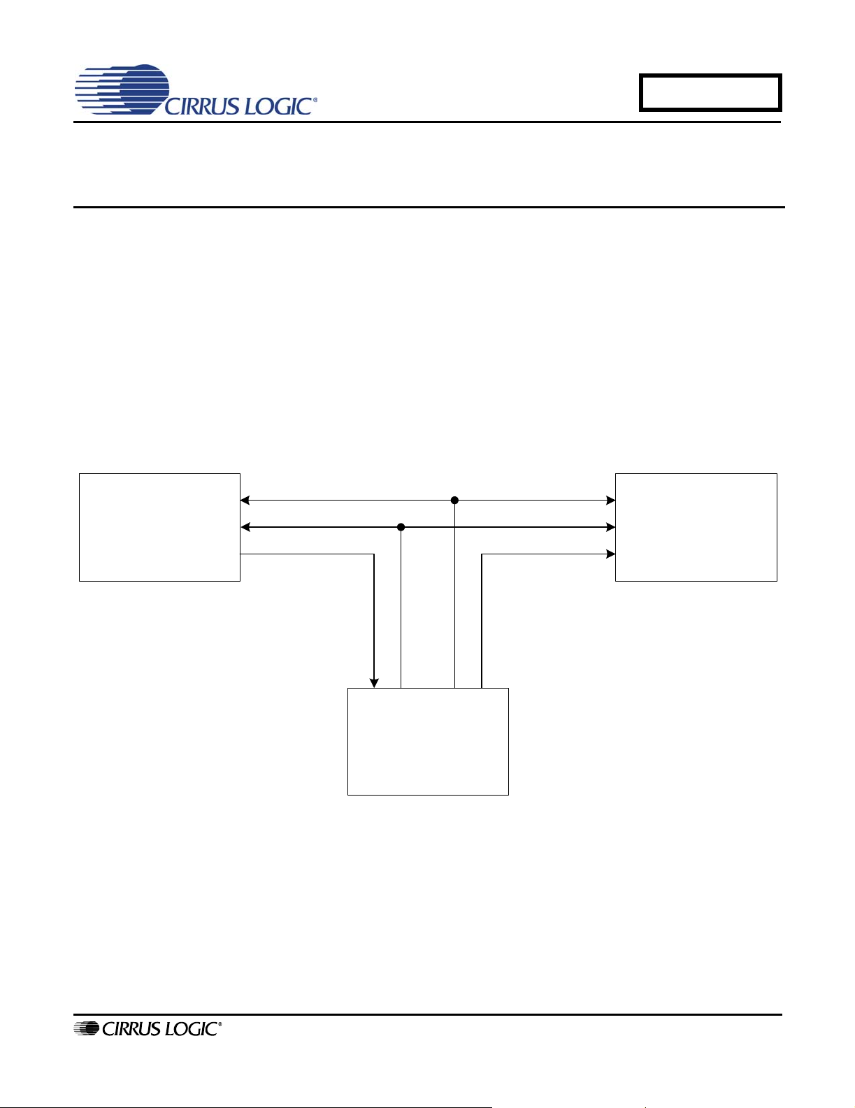
term Serial Audio Interface (SAI) in this discussion. The Serial Audio Interface is by far the most common mechanism used to transfer two channels of audio data between devices within a system; for instance, from the analogto-digital converter to the Digital Signal Proc essor (DSP) and then the digital-to-analog converter, as shown in
Figure 1.
Left / Right Clock
Analog-to-Digital Converter Digital-to-Analog Converter
DSP
Figure 1 System Block Diagram
Serial Clock
Serial DataSerial Data
http://www.cirrus.com
Copyright © Cirrus Logic, Inc. 2005
(All Rights Reserved)
JUNE '05
AN282REV1
Page 2
AN282
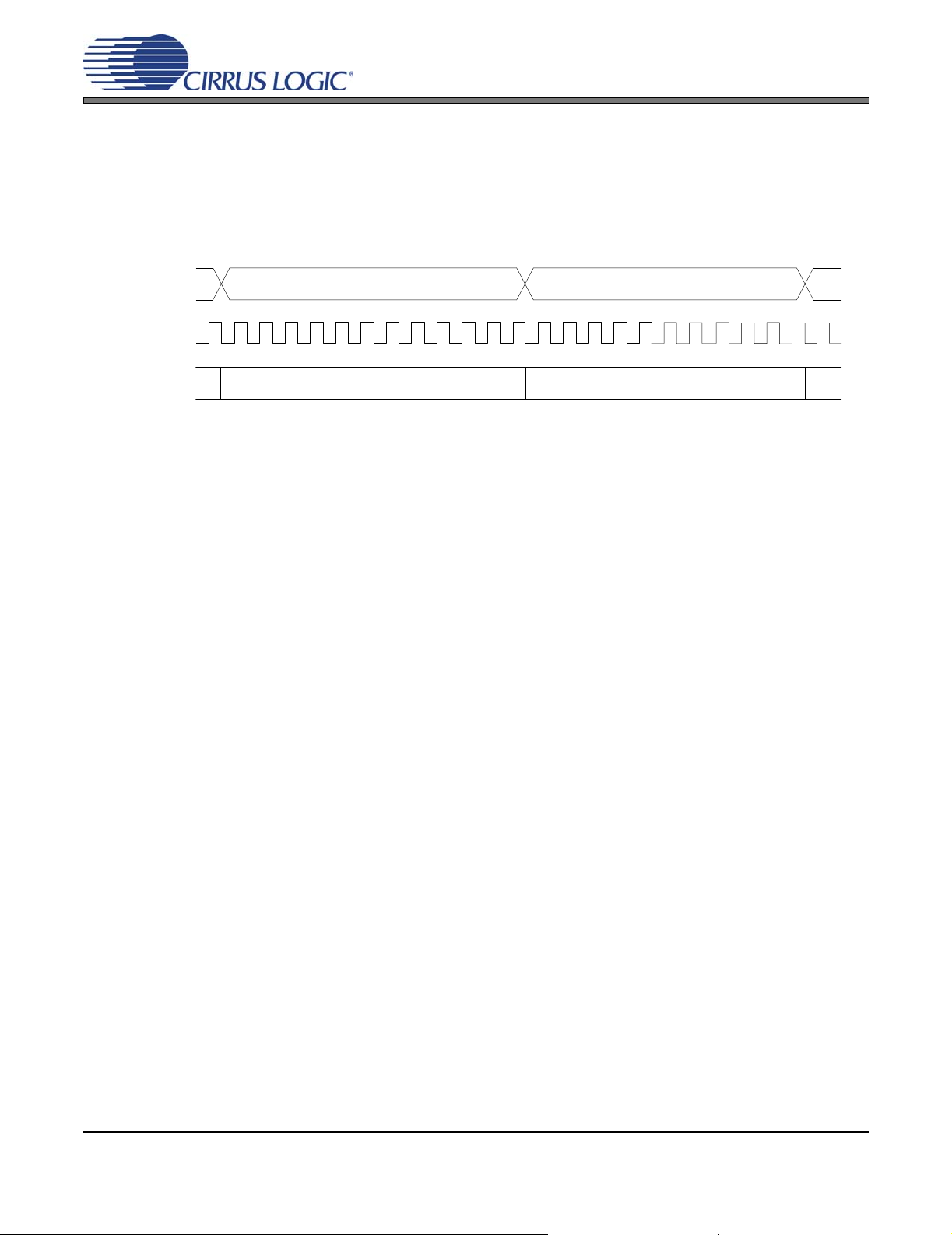
1. THE SERIAL AUDIO INTERFACE
The Serial Audio Interface is comprised of two control clocks, the Left / Right and Serial Clocks, and the Serial audio
data line. Despite the many different names used for the various clocks, their uses and requirements are nearly identical. A generalized Serial Audio Interface is shown in Figure 2. Some form of this diagram can probably be found
in every audio converter and DSP data sheet that has ever been published.
Left/Right Clock
Serial Clock
1.1 Left/Right Clock
The Left/Right (LRCK) Clock is known by several names, including Word Clock, Frame Clock, Frame Sync,
and probably several others. Despite the differ ent name s, the use and require ments for this clocking signal
are identical. In all applications, the function of this clock signal to id entify the audio system sample rate and
frame the two channels of audio data that exist on the single audio data line. As a result of the first mentioned function, the required frequency of the Left/Right Clock signal is always at the system audio sample
rate, such as 44.1 kHz, 48 kHz, etc. The high and low times of this clock are used to separate or delineate
the Left and Right channel data.
1.2 Serial Audio Data
The industry standard for representing Pulse-Coded-Modulation (PCM) audio data is a word comprised of
16 to 32 bits (16- and 24-bit data are the most common) coded in a two’s-complement format. The audio
data word is always transmitted with the Most Significant Bit (MSB) first. The only common exception to the
two’s-complement format is when the audio data is represented in one of the many compressed audio formats.
1.3 Serial Clock
Audio Data
Figure 2 Generic Serial Audio Interface Diagram
Audio Data
The Serial Clock (SCLK) is also often referred to as the Bit Clock. As with the Left/Right Clock, the function
is the same regardless of the name. The sole purpose of the Serial Clock is to shift the audio data into or
out of the serial audio port. The m inimu m req uire d freq uency f or t he Seri al Cl ock is direc tly pro port ional to
the system audio sample rate and the audio word length. Recall that there are two channels of audio data
presented in each period of the Left/Rig ht Clock, a nd the frequency of the Left/Right Clock must be at the
audio sample rate. Therefore, the minimum required Serial Clock frequency is twice the audio sample rate
times the number of bits in each audio word.
2 AN282REV1
Page 3

AN282
2. THE SERIAL AUDIO INTERFACE FORMATS
There are several de-facto industry standards or formats that define the required alignments and signal polarities
between the Left/Right Clock, Serial Clock and the Serial audio data.
2.1 Left-Justified Data Format
The Left-Justified (LJ) format probably got its name from the relationship of the audio data and the Le ft/Right
Clock. Refer to Figure 3 and notice that the MSB of th e audio word is coincident with the leading transitions
in the Left/Right Clock, or left-justified within the frame. One of the advantages of this format is that it is wordlength independent and works properly with aud io data words of 16 to 32 bits, assuming there is a sufficient
number of serial clocks per Left/Right clock cycle.
Another important aspect of the LJ format is that the audio data for the left channel is presented on the serial
data line during the high portion of the Left/Right Clock, and the right channel is presented during the low
portion.
LRCK
SCLK
SDATA +3 +2 +1+5 +4
-1 -2 -3 -4 -5
MSB LSB MSB LSB
Left Channel
Figure 3 Standard Left-Justified Format
2.2 Right-Justified Data Format
Referring to Figure 4, it is relatively apparent that the Right-Justified (RJ) format is very similar to the LeftJustified format, with the exception of the placement of the audio word within the frame. Notice that the trailing edge of the LSB is coincident with the trailing edge of the Left/Right Clock, or right-justified within the
audio frame. The primary disadvantage of this format is that the interface is not word-length independent.
As a result, any device that is receiving data in a Right-Justified format must be aware of the transmitted
audio word length. This explains why most Digital-to-Analog (D/A) converters are required to support multiple right-justified formats.
As with the Left-Justified format, the audio data for the left ch annel is presented on the serial data line during
the high portion of the Left/Right Clock, and the right channel is presented during the low portion.
LRCK
SCLK
Left Channel
-1 -2 -3 -4
Right Channel
+3 +2 +1+5 +4
Right Channel
SDATA
6+5+4 +3 +2
0
MSB-1-2-3-4-5
32 clock
7
+1 LSB
MSB-1-2-3-4-5
6+5+4 +3 +2
7
+1 LSB
Figure 4 Standard Right-Justified Format
AN282REV1 3
Page 4

AN282
2.3 I²S Data Format
The “Inter-IC Sound” bus (I²S) format was originally developed and standardized by Philips Electronics. The Philips
I²S specification can be found at http://www.semiconductors.philips.com/acrobat_download/various/I2SBUS.pdf.
Referring to Figure 5, it is relatively apparent that there are significant difference s between I²S and the other formats.
While I²S retains the word-length independence of the Left-Justified format, notice that the left channel of data is
framed by the low time of the Left/Right Clock and the right channel is framed by the high time. Another significant
difference is that the MSB of the audio word is shifted or delayed one period of the Serial Clock from the leading
edge of the Left/Right Clock.
LRCK
SCLK
SDATA +3 +2 +1+5 +4
-1 -2 -3 -4 -5
MSB
3. TIME ALIGNMENT
A very important aspect of the Serial Audio Interface is the fact that the left/right sample pairs represent
simultaneously sampled data or time-aligned data. Another way to look at this relationship is shown in
Figure 6, where the same signal is connected to both inputs of an Analog-to-Digital converter. Analyzing the
data in left/right sample pairs shows that the left and right channels are time-aligned. However, if the data
is analyzed as right/left sample pairs, the signals appear to be time-shifted in relation to each other by ∆T,
as shown in Figure 7, where ∆T is equivalent to 1 period of the audio system sample rate.
Left Channel
Right Channel
LSB LSB
MSB
-1 -2 -3 -4
+3 +2 +1+5 +4
Figure 5 Standard I²S Format
Figure 6 Left/Right Sample Pairs in Time Alignment
T
Figure 7 Right/Left Sample Pair in Time Misalignment
4 AN282REV1
Page 5

AN282
4. IMPLEMENTATIONS OF MORE THAN TWO CHANNELS
The Serial Audio Interface can be easily scaled to support larger channel counts simply by adding the appropriate
number of serial audio data lines while retaining the single Serial Clock and Left/Right Clock, as shown in Figure 8.
Left / Right Clock
A / D #1
A / D #2
Serial Clock
Serial Data
Serial Data
DSP
Figure 8 Multi- Channel Serial Audio Interface Diagram
Serial Data
Serial Data
D / A #1
D / A #2
AN282REV1 5
Page 6

5. REVISION HISTORY
Release Date Changes
Revision 1 June 2005 Initial Release
AN282
Contacting Cirrus Logic Support
For all product questions and inquiries contact a Cirrus Logic Sales Representative.
To find the one nearest to you go to www.cirrus.com
IMPORTANT NOTICE
Cirrus Logic, Inc. an d i t s s ubs i di ari es ( "Cir r us ") be li e ve th at t he in for mat i on con ta in ed in t hi s do cumen t i s acc ura t e and re liable. However, the i nf or ma ti on is s u bj ect
to change without notice and is provide d "AS IS" witho ut warranty of any kind (exp ress or impl ied). Cust omers are advise d to obtain the latest version of relevant
information to verify, before placing orders, that information being relied on is current and complete. All products are sold subject to the terms and conditions of sale
supplied at the time of order acknow ledgment, incl uding those per taining to warranty, ind emnification, an d limitation of liabi lity. No responsibility is assumed by Cirrus
for the use of this information, including use of this information as the basis for manufacture or sale of any items, or for infringement of patents or other rights of third
parties. This document is the property of Cirrus and by furnishing this information, Cirrus grants no license, express or implied under any patents, mask work rights,
copyrights, trademarks, trade secrets or other intelle ctual property rights. Cirrus o wns the copyr ights associated with the information contained herein and gives consent for copies to be made of the information only for use within your organization with respect to Cirrus integrated circuits or other products of Cirrus. This consent
does not extend to other copying such as copying for general distribution, advertising or promotional purposes, or for creating any work for resale.
CERTAIN APPLICATIONS USING SEMICONDUCTOR PRODUCTS MAY INVOLVE POTENTIAL RISKS OF DEATH, PERSONAL INJURY, OR SEVE RE PROPERTY OR ENVIRONMENTAL DAMAGE (“CRITICAL APPLICATIONS”). CIRRUS PRODUCTS ARE NOT DESIGNED, AUTHORIZED OR WARRANTED FOR USE
IN AIRCRAFT SYSTEMS, MILITARY APPLICATIONS, PRODUCTS SURGICALLY IMPLANTED INTO THE BODY, AUTOMOTIVE SAFETY OR SECURITY DEVICES, LIFE SUPPORT PRODUCTS OR OTHER CRITICAL APPLICATIONS. INCLUSION OF CIRRUS PRODUCTS IN SUCH APPLICATIONS IS UNDERSTOOD
TO BE FULLY AT THE CUSTOMER’S RISK AND CIRRUS DISCLAIMS AND MAKES NO WARRANTY, EXPRESS, STATUTORY OR IMPLIED, INCLUDING THE
IMPLIED WARRANTIES OF MERCHANTABILI TY AND FITNESS FOR PARTICULAR PURPOSE, WITH REGARD TO ANY CIRRUS PRODUCT THAT IS USED
IN SUCH A MANNER. IF THE CUSTOMER OR CUSTOMER’S CUSTOMER USES OR PERMITS THE USE OF CIRRUS PRODUCTS IN CRITICAL APPLICATIONS, CUSTOMER AGREES, BY SUCH USE, TO F ULLY INDEMNIFY CIRRUS, ITS OF FICERS, DIRECTORS, EMPLOYEES, DIST RIBUTORS AND OTHER
AGENTS FROM ANY AND ALL LIABILITY, INCLUDING ATTORNEYS’ FEES AND COSTS, THAT MAY RESULT FROM OR ARISE IN CONNECTION WITH
THESE USES.
Cirrus Logic, Cirrus, and the Cirrus Logic logo designs are trademarks of Cirrus Logic, Inc. All other brand and product names in this document may be trademarks
or service marks of their respective owners.
6 AN282REV1
 Loading...