

Page 1
AN270
Audio A/D Conversion
with an Asynchronous Decimation Filter
Steve Green
Technical Marketing Manager
Thomas Hoff
Applications Engineer
1. INTRODUCTION
Modern high-performance delta-sigma anal og-to-digital (A/D ) and digital-to- analog (D/A) audio conversio n systems
require a high frequency system clock (master clock) for their conversion processes, generally in excess of 12 MHz.
Jitter on this clock is a significant source of performance degradation in these systems. Th is is generally n ot a problem in products that include the converters as well as a crystal based clock. However, this can be a particularly difficult problem to address in networked audio systems, recording systems which utilize a “house sync” signal and
other systems that require long-distance routing of the high frequency clocking signal within the system, such as a
mixing console. A common denominator of these systems is that the conversion nodes and the network operate at
the same sample rate or within the same clock domain. The most common approach to recover a low-jitter master
clock in these systems is to make use of a phase-lock-loop (PLL). PLL circuits take several forms and have their
advantages. However, often times the jitter performance is less than desirable or the PLL does not have a sufficient
frequency range, especially in voltage controlled crystal oscillator circuits, to cover all of the required sample rates.
An alternative approach is to create a system architecture where the A/D and D/A conversion nodes o perate withi n
local clock domains which are independent of the network or system clock domain. A system with independent clock
domains can easily be accomplished with the use of a sample rate converter (SRC), as shown in Figure 1. This architecture also allows the conversion processes to operate at a fixed sample rate which is always higher than the
network or interface sample rate. The fundamental advantage of this approach is that the co nversion processes are
immune to interface clock jitter and are controlled by a local jitter-free crystal oscillator.
Crystal
Osc illator
CS5381
A/D
A/D Sampling
Clock Domain
http://www.cirrus.com
System
Word Clock
CS8421Asynchronous
Sample Rate Conv erter
Clock Domain
Figure 1. Audio System Architecture with Independent Clock Domains
Copyright © Cirrus Logic, Inc. 2005
DSP
Interface
(All Rights Reserved)
CS8421Asynchronous
Samp le Rate Co n v e rte r
Crystal
Oscillator
D/A Conversion
CS4398
D/A
Clock Domain
MAY '05
AN270REV1
Page 2

AN270
It is interesting to look at this application from a different perspective. Modern A/D converters utilize digital decimation filters which convert the highly over sampled data to the standard audio sample rates o f 44.1, 48, 96 or 192 kHz.
These decimation filters perform this function in a synchronous manner where the ratio of the input to output sample
rates is fixed, generally either 512, 256 or 128. Essentially, these digital filters downsample the A/D sampled data
to a lower sample rate in a synchronous manner. A similar procedure occurs with the digital interpolation filter in the
D/A conversion process where the input sam ple rate is r aised to a high er sample rate pr ior to the d igital-to -analog
conversion. Consider the fact that in the proposed application the conversion processes can easily be configured
such that the A/D and D/A conversions are always operating at a higher sample rate than the interface or network.
In this configuration, the SRC is operating as either a decimation or interpolation filter bu t in an asynchronous manner. Essentially, the integer multiple constrain t imposed by standar d synchronous decimat ion and interpolatio n filters no longer applies. It is this attribute that allows the conversion processes to operate in clock domains which are
independent of the network or interface.
In this application, the output of the CS8421 is configured as a slave to the interface system clock. T here are several
advantages to this approach. The first is the simplicity of changing the system sample rate. Since the conversion
process is operating asynchronously from the network, a simple change of the network Left/Right or Word clock is
all that is required to change the system sample rate, si nce the outpu t sample rate of th e SRC is dete rmined by the
input Word clock. There is no longer a need to reconfigure e ither the A/D or D/A converters for changes in the system
sample rate. The second advantage is that the fact that the output sample rate is dependent on the fre quency of the
incoming word clock which ensures that the outputs of multiple CS8421 devices are synchronous and phasematched. The third advantage is that it allows multiple devices to be configured in a Time Division Multiplex (TDM)
multi-channel interface.
2. ADDITIONAL FEATURES
The inclusion of the CS8421 in the system also adds additional, and valuable, functionality. Th ese unique functions
address many of the issues and design challenges associated with networked audio systems and other high-performance multi-channel applications.
• Selectable Output Data Resolution - The CS8421 utilizes full 32-bit internal processing and provides the
option to output the full 32-bit data word. In addition to the full precision 32-bit data, the device ha s the functionality to properly dither and truncate the 32-bit data to word lengths of either 24, 20 or 16-bits. Th e dither
between left and right channels is uncorrelated.
• Support for all Industry Standard Data Formats - The CS842 1 supports all of the industry standard data
formats including Left-Justified, Right-Justified and I
mentation using these formats.
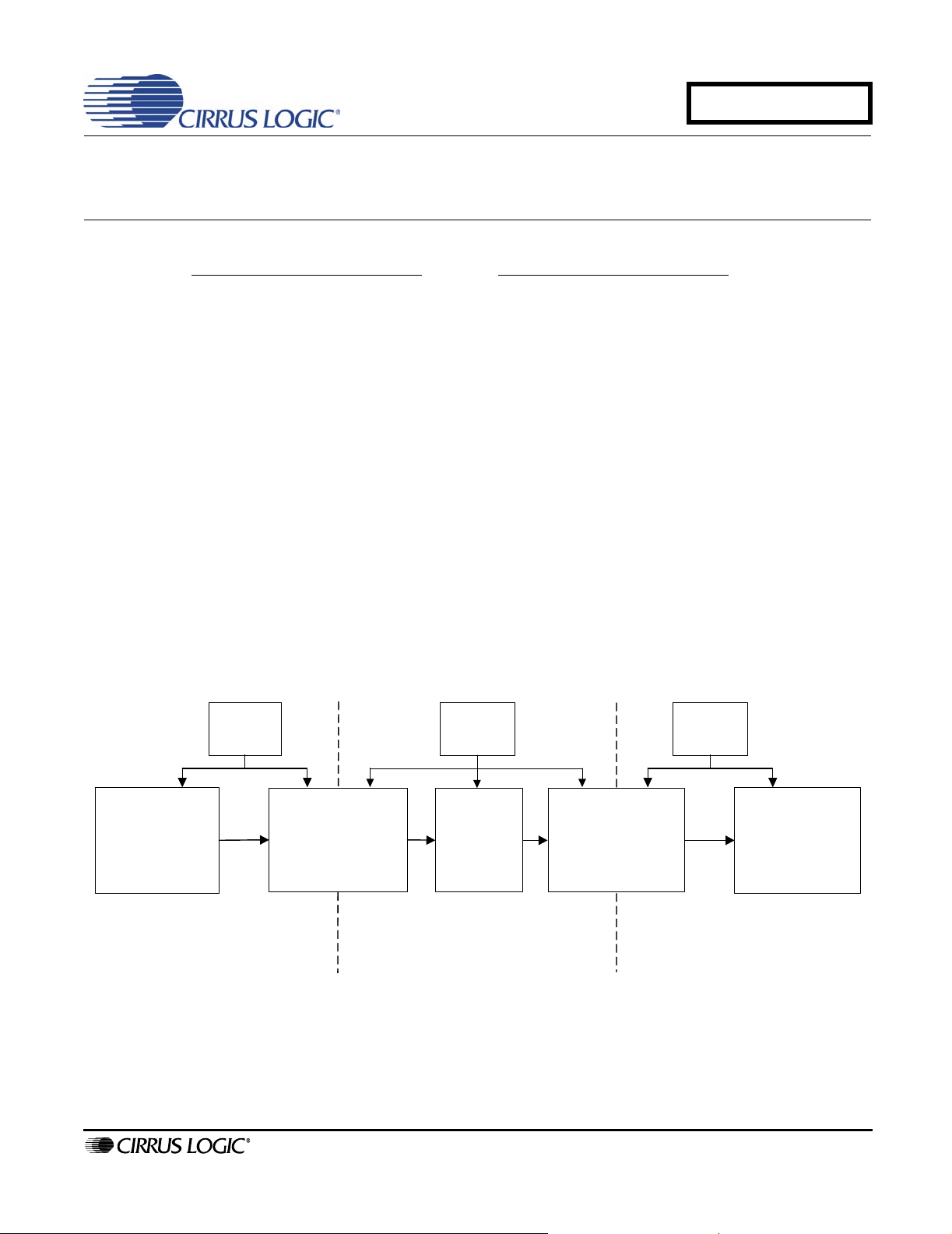
• Multi-Channel TDM Interface - In addition to the standard serial audio interface, multiple CS8421 devices
can be configured to implement a multi-channel Time Division Multiplex (TDM) interface. The CS8421 can
support a 4-channel TDM at 192 kHz, 8-channels at 96 kHz and 16-channels at 48 kHz sample rates. The
block diagram for a 6-channel TDM implementatio n is sh own in Figu re 3. Additional cha nnels can easily be
added.
• Greater Digital Stopband rejection over the CS5381 - The digital filter in the CS8421 do minates the filter
response in this application. As a result, the minimum stopband rejection is 125 dB.
2
S. Figure 2 illustrates a typical multi-channel imple-
2 AN270REV1
Page 3

Interface
Clock
Domain
AN270
SDATA2
SDATA1
LRCK
SCLK
CS8421 CS8421
LRCK SCLK SDOUT
Interface
Clock
Domain
SDATA
CS5381
LRCK
SCLK
OLRCK
OSCLK
SDOUT1TDM _IN
ILRCK
IS C L K
SDIN
LRCK SCLK SDOUT
CS5381
Figure 2. 4-Channel Serial Audio Interface Configuration
OLRCK
OSCLK
SDOUT2TDM _IN
ILR C K
IS C L K
SDIN
CS8421 CS8421 CS8421
OLRCK
OSCLK
SDOUTTDM_IN
LRCK SCLK SDOU T
CS5381
ILR CK
ISC L K
SDIN
OLRCK
OSCLK
SDOUTTDM_IN
LRCK SCLK SDOUT
CS5381
ILR C K
ISC L K
SDIN
OLRCK
OSCLK
SDOUTTDM_IN
ILRCK
ISC L K
SDIN
LRCK SCLK SDOU T
CS5381
Figure 3. 6-Channel TDM Configuration
AN270REV1 3
Page 4

AN270
3. CRD5381 OVERVIEW
The CRD5381 is a 4-channel reference design that combines the CS5381 Analog-to-Digital Conver ter and CS8421
Asynchronous Sample Rate Converter to create an analog-to-digital conversion system as described in this applications note. The CRD5381 is essentially a 2-channel design where the 2-channel block has been replicated to create the 3
converter and the CS8421 Asynchronous Sample Rate converter. The refe rence desig n also includes clock ge neration, status reporting and the required system reset functions. In addition, the dual CS8421 devices can be configured for a 4-channel Time Division Multiplex (TDM) interface.
The intent of the CRD5381 and supporting documentation is to create a de sign r eference that can be co nsidere d a
“cut and paste” reference to create a multi-channel A/D conversion system. Please also refer to the CS5381 and
CS8421 data sheets for specific product information and specifications. These documents are available online at
http://www.cirrus.com. The CRD5381 reference design is also available from Cirrus Logic.
The following are the typical performance specifications that can be expected from a CRD5381-based design.
rd
and 4th channels. Each 2-channel section includes the required analog input buffer, the CS5381 A/D
• Dynamic Range (A-weighted) — 120 dB
• Total Harmonic Distortion + Noise — -110 dB
• Resolution — 16 to 32 bits
• Maximum Downsampling Ratio — 7.5:1
• Minimum Stopband Attenuation — 125 dB
Contacting Cirrus Logic Support
For all product questions and inquiries contact a Cirrus Logic Sales Representative.
To find the one nearest to you go to
IIMPORTANT NOTICE
Cirrus Logic, Inc. and its subsidiaries (“Ci rrus”) believe that t he information contained in this document is accurate and reliable. However, the information is subject
to change without noti ce and is pro vided “AS I S” without warranty of any kind (express o r impli ed). Cust omers are adv ised to ob tain the latest version of relevant
information to verify, before placing orde rs, that i nforma tion b ein g re lied on is curren t a nd com plete. All p roducts are so ld s ubject to the terms and conditions of sale
supplied at the time of order acknowledgment, including those pertaining to warranty, indemnification, and limitation of liability. No responsibility is assumed by Cirrus
for the use of this information, including use of this information as the basis for manufacture or sale of any items, or for infringement of patents or other rights of third
parties. This document is the property of Cirrus and by furnishing this information, Cirrus grants no license, express or implied under any patents, mask work rights,
copyrights, trademarks, trade secrets or other inte llectual property rights. Cirrus owns the copyrights associated with the information contained herein and gives consent for copies to be made of the information only for use within your organization with respect to Cirrus integrated circuits or other products of Cirrus. This consent
does not extend to other copying such as copying for general distribution, advertising or promotional purposes, or for creating any work for resale.
CERTAIN APPLICATIONS USING SEMICONDUCTOR PRODUCTS MAY INVOLVE POTENTIAL RISKS OF DEATH, PERSONAL INJURY, OR SEVERE PROPERTY OR ENVIRONMENTAL DAMAGE (“CRITICAL APPLICATIONS”). CIRRUS PRODUCTS ARE NOT DESIGNED, AUTHORIZED OR WARRANTED FOR USE
IN AIRCRAFT SYSTEMS, MILITARY APPLICATIONS, PRODUCTS SURGICALLY IMPLANTED INTO THE BODY, AUTOMOTIVE SAFETY OR SECURITY DEVICES, LIFE SUPPORT PRODUCTS OR OTHER CRITICAL APPLICATIONS. INCLUSION OF CIRRUS PRODUCTS IN SUCH APPLICATIONS IS UNDERSTOOD
TO BE FULLY AT THE CUSTOMER’S RISK AND CIRRUS DISCLAIMS AND MAKES NO WARRANTY, EXPRESS, STATUTORY OR IMPLIED, INCLUDING THE
IMPLIED WARRANTIES OF MERCHANTABILITY AND FITNESS FOR PARTICULAR PURPOSE, WITH REGARD TO ANY CIRRUS PRODUCT THAT IS USED
IN SUCH A MANNER. IF THE CUSTOMER OR CUSTOMER’S CUSTOMER USES OR PERMITS THE USE OF CIRRUS PRODUCTS IN CRITICAL APPLICATIONS, CUSTOMER AGREES, BY SUCH USE, TO FULLY I NDEMNIFY CIRRUS , ITS OFFI CERS, DIRECTORS, EMPLOYEES, DISTRIBUTORS AND OTHER
AGENTS FROM ANY AND ALL LIABILIT Y, INCLUDING ATTORNEYS’ FEES AND COSTS, THAT MAY RESULT FROM OR ARISE IN CONNECTION WITH
THESE USES.
Cirrus Logic, Cirrus, and the Cirrus Logic logo design s ar e tra de m a rks of Cir rus Lo gic, Inc. A ll oth er bra nd an d p ro du c t names in this document may be trademarks
or service marks of their respective owners.
www.cirrus.com
4 AN270REV1
 Loading...