

Page 1
AN269
Using the EP93xx's Raster Engine
1. INTRODUCTION AND SCOPE
The purpose of this document is to he lp a u ser und er st and how to conn ect an LCD module to the EP93xx serie s of
embedded processors from Cirrus Logic. A wide variety of timings and output settings are available, which allows
connection to many color and black-and-white LCD displays. Some timing modes will also allow connection to an
external video DAC, which can be used to drive any type of display.
This application note is focused on th e typical usage of certain exampl e LCD screens. As such, the examples were
designed and tested at typical values to show how the LCD controller can be used. If plannin g to use the LCD controller outside these typical cases, the user should test and verify the application in the target environment. In addition, this document is not a replaceme nt for the information in the EP93xx User's Guide and the EP93xx Data
Sheet. It should be used in conjunction with these documents. It is highly recommended that the user read the
EP93xx User Guide chapter titled "Raster Engine With Analog/LCD Integrated Timing and Interface" before using
this Application Note.
Throughout this document, signals will be identified in diagrams and equations by their corresponding EP93xx signal
names, unless otherwise specified.
2. HOW TO DETERMINE IF AN LCD IS COMPATIBLE WITH THE EP93XX
The EP93xx raster engine is very versatile, and will work with a variety of LCD display types. In order to determine
if a display is compatible, follow these steps:
1. Check the appendices at the back of this manual to see if the display is listed as an example. If so, use the
specified register settings for that display. Otherwise, proceed to step 2.
2. Examine the waveforms in Figures 9, 14, and 20. If the desired displa y timings match any of these diagrams
(or vary only in signal polarity), Section 6, 6.2, or 6.3 will describe how to set up the EP93xx raster timing
registers. If the display does not match any of these, refer to “Other Types of Framed Data Displays” on
page 41 for more information. Note that the sig nals AC, XECL, and YSCL are not discus sed in these d ia-
grams, but are described in the “Video Timing” section of the Raster Engine chapter of the EP93xx User’s
Guide.
3. After determining that the sy nchronization signals can be generated by the EP93xx, the appropriate pixel
output mode should be chosen. “General Description of Pixel Output Modes” on page 9 describes this pro-
cess.
If the timing requirements or the pixel input format of the display are not supported, than the display may still be
supported using GPIO pins to generate the appropriate timings. However, this will consume much more processor
time, but may be a viable option for slower/smaller displays.
The versatility of the EP93xx raster engine attempts to cover the most common types of displays. Even though care
has been taken in the design of this block, please keep in mind that not all LCD panels can be supported.
http://www.cirrus.com
Copyright © Cirrus Logic, Inc. 2005
(All Rights Reserved)
AUG '05
AN269REV1
Page 2
AN269
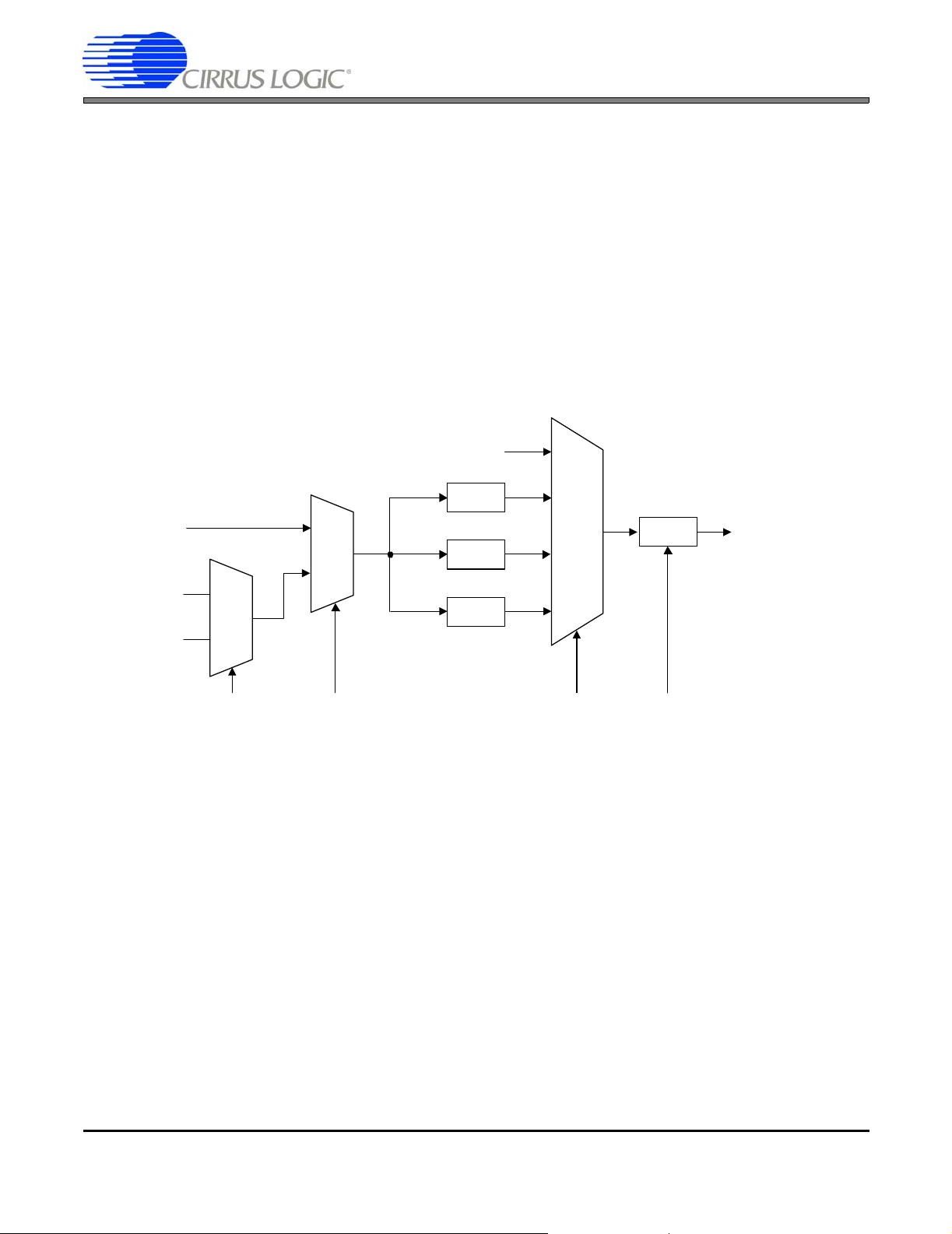
3. GENERATION OF THE VIDEO CLOCK, VIDCLK
The internal video clock (VIDCLK), which drives the raster engine and the external pixel clock (SPCLK), is derived
from PLL1, PLL2, or the external clock input. The SPCLK signal clocks data fr om the EP9 3xx into the exter nal LCD
or display. The number of pixels per SPCLK may be 1, 2, 4, 8, or 2-2/3.
Conceptually, the external clock (SPCLK) is generated by di viding the VIDCLK by the appropriate clock divider. The
necessary divider depends on the output mode. For 1 pixel-per-SPCLK, there will be 1 VIDCLK-per-SPCLK. For 2
pixels-per-SPCLK, there will be 2 VIDCLKs-per-SPCLK (SPCLK runs at VIDCLK/2). For the case of 4 pixels-perSPCLK, there are 4 VIDCLKs-per-SPCLK. Note that 2-2/3 mode is a special case in which there are 3 VIDCLKs for
the first SPCLK, 2 for the second SPCLK, and 3 for the third SPCLK. This pattern then repeats every 8 pixels (and
therefore 8 VIDCLKs).
To derive VIDCLK, the clock source (PLL1, PLL2, or External Clock) is divided by a prescaler and then by a divideby-N block, where N
VDIV are all bit fields of the VidClk Div register, contained in the system controller. Please refer to the EP93xx User’s
Guide (“System Controller” section) for more information on the VidClkDiv register.
≥ 2. This is shown in the block diagram in Figure 1. The values of PSEL, ESEL, PDIV, and
Disable
÷ 2
External
Clock
PLL1
PLL2
Below is one algorithm for integer math operations (similar to the Linux 2.6 video display driver) for determining the
proper VidClkDiv settings for a desired VIDCLK rate. Essentially, the algorithm examines the frequency of the external clock source, PLL1, and PLL2, and then attempts differ ent combinations of the divider settings to find a setting
that generates the smallest error. The divider settings are a combination of PDIV (pre-divider) and VDIV (divide-by-
N). Since PDIV can be set to 2, 2.5, or 3, the algorithm uses twice that value (and therefore twice the value of the
PLL1, PLL2, etc.). Note that the accuracy of this algorithm may be improved through the use of floating-point math.
0
1
PSEL
0
÷ 2.5
1
÷ 3
ESEL
Figure 1. Video Clock Generation
00
01
10
11
PDIV
÷ N
VDIV
(≥ 2)
Video Clock
Output
(To Raster
Block)
2 AN269REV1
Page 3

/* Desired SPCLK frequency is passed in as "freq" */
int ep93xx_set_video_div(unsigned long freq)
{
/* pdiv, div, psel and esel are the final values of the appropriate bit settings in the
VidClkDiv register. The current "guess" for pdiv and div are j-3 and k, respectively. */
unsigned long pdiv = 0, div = 0, psel = 0, esel = 0, err, f, i, j, k;
/* Algorithm may return -1 if no valid setting can be found */
err = -1;
/* Try the External Clock, PLL1 an d PLL2 */
for (i = 0; i < 3; i++) {
if (i == 0)
/* The External Clock, multiplied by 2 */
f = 14745600 * 2;
else if (i == 1)
/* PLL1 output frequency, multiplied by 2 */
f = ep93xx_get_pll_frequency(1) * 2;
else
/* PLL2 output frequency, multiplied by 2 */
f = ep93xx_get_pll_frequency(2) * 2;
/* Try each setting of PDIV, the pre-divider , and look for a VDIV
setting that would give us the desired frequency. Note that we are
using PDIV*2, since we multiplied the frequency by 2 above. */
for (j = 4; j <= 6; j++) {
k = f / (freq * j);
if (k < 2) {
/* VDIV must be at least 2 */
continue;
}
AN269
/* Calculate how far off of the desired frequency this setting is,
and then set the values of PDIV and VDIV from j and k.
At this point, the clock source is set, also. */
if (abs(((f / (j * k))) - freq) < err) {
pdiv = j - 3;
div = k;
psel = (i == 2) ? 1 : 0;
esel = (i == 0) ? 0 : 1;
err = (f / (j * k)) - freq;
}
}
}
if (err == -1) {
/* We were unable to determine a setting that is appropriate */
return -1;
}
/* Unlock the registers */
outl(0xaa, SYSCON_SWLOCK);
/* Write the values to the registers */
outl(SYSCON_VIDDIV_VENA | (esel ? SYSCON_VIDDIV_ESEL : 0) |
(psel ? SYSCON_VIDDIV_PSEL : 0) |
(pdiv << SYSCON_VIDDIV_PDIV_SHIFT) |
(div << SYSCON_VIDDIV_VDIV_SHIFT), SYSCON_VIDDIV);
/* Return the actual value of what frequency we set */
return freq + err;
}
AN269REV1 3
Page 4

AN269
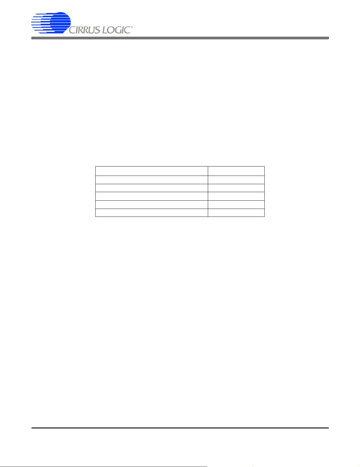
4. USING THE HORIZONTAL AND VERTICAL COUNTER FOR TIMINGSIGNAL GENERATION
Conceptually, all timing synchronization outputs from the EP93xx are driven from a series of down counters followed
by combinational logic. The input clock to these counters is the video clock signal, VIDCLK (see “Generation of the
Video Clock, VIDCLK” on page 2). There are two banks of down counter/comparators - one for horizontal and one
for vertical timing generation. A block diagram of the horizontal and vertical timing generation is shown in Figure 2,
and brief descriptions of each of the corresponding timing registers are found in Table 1.
REGISTER DESCRIPTION
VLINESTOTAL
Vertical Lines Total
VSYNCSTRTSTOP
Vertical Sync Pulse Start/Stop
VACTIVESTRTSTOP
Vertical Active Start/Stop
VBLANKSTRTSTOP
Vertical Blank Start/Stop
VCLKSTRTSTOP
Vertical Clock Start/Stop
HLINESTOTAL
Horizontal Lines Total
HSYNCSTRTSTOP
Horizontal Sync Pulse Start/Stop
HACTIVESTRTSTOP
Horizontal Active Start/Sto p
HBLANKSTRTSTOP
Horizontal Blank Start/Stop
HCLKSTRTSTOP
Horizontal Clock Start/Stop
VIDEOATTRIBS
Video Signal Attributes
Table 1. Summary of Synchronization Registers
Total number of horizontal lines in a single video frame (Includ-
ing SYNC, BLANK & ACTIVE regions).
Vertical counter: Defines when the VCSYNC pulse becomes
active (Start) and goes inactive (Stop)
Vertical counter: Defines when the VACTIVE signal becomes
active (Start) and goes inactive (Stop). This internal signal is
OR’d with HACTIVE to define the active portion of the video
frame (when active pixel data is clocked out).
Vertical counter: Defines when the VBLANK signal becomes
active (Start) and becomes inactive (Stop) before and after the
active video portion of the video frame. BLANK is the AND of
HBLANK and VBLANK.
Vertical counter: Defines when the VCLKEN Signal goes active
(Start) and becomes inactive (Stop) at the beginning or end of
the video frame. SPCLK is only generated when the VCLKEN
and HCLKEN signals are BOTH active.
Total Number of VIDCLKs in a single horizontal line of video,
including both active and inactive regions.
Horizontal counter: Defines when the HSYNC pulse becomes
active (Start) and goes inactive (Stop).
Horizontal counter: Defines when the HACTIVE signal
becomes active (Start) and goes inactive (Stop). This signal is
OR’d with VACTIVE to define the active portion of the video
frame (when active pixel data is clocked out).
Horizontal counter: Defines when the HBLANK signal
becomes active (St art) and becomes inactive (Stop) before
and after the active video portion of the video frame. BLANK is
the AND of HBLANK and VBLANK.
Horizontal counter: Defines when the HCLKEN Signal goes
active (Start) and becomes inactive (Stop) at the beginning or
end of the video frame. SPCLK is only generated when the
VCLKEN and HCLKEN signals are BOTH active.
Synchronization Control, Polarity Selection, Output Enables,
etc.
The video clock (VIDCLK) decrem ent s the h orizon tal do wn counter at one count per video clock period. When the
count reaches 0, the counter loads the value contained in the HClkTotal register, and continues co unting down. The
HSYNC output is generated by comparing the value of the horizontal down counter with the HSyncStrtStop register.
If the value of the counter is in the active range (HSyncStrtStop.Start > Horizontal Counter > HSyncStrtStop.Stop),
the HSYNC output becomes active. Similarly, the HBlankStrtStop, HActiveStrtStop, and HClkStrtStop values are
compared with the horizontal down counter, and then control the BLANK Output, Pixel Output Enable, and Pixel
Clock Output Enable (once combined with the appropriate signals from the vertical timing block).
4 AN269REV1
Page 5
AN269
When the output of the horizontal down counter rolls over, it will decrement the vertical down counter at one count
per horizontal line. When the count reaches 0, the vertical down counte r loads the value contained in the VLinesTo-
tal register, and continues counting down. The VCSYNC ou tput is ge ne rate d by compar ing the value of the ve rtical
down counter with the VSyncStrtStop register. If the value of the counter is in the active range (VSyncStrtStop.Start
> Vertical Counter > VSyncStrtStop.Stop), the VCSYNC output becom es active. Similarly the VBlankStrtStop, VAc-
tiveStrtStop, and VClkStrtStop values are compared with the vertical down counter, and then control the BLANK
Output, Pixel Output Enable, and Pixel Clock Output Enable (once combined with the appropriate signals from the
horizontal timing block).
4.1 Counter Offsets
Due to internal delays inside the raster timing block, various register settings must be offset to align data,
sync, and clock outputs properly at the output of the ep93xx. In the following sections, th ese delays are added at the last stage of computing the timings (when setting the actual register values).
These delays are listed in Table 2.
Registers Offset in SPClocks
HSYNCSTARTSTOP 0
HACTIVESTRTSTOP -1
HACTIVESTRTSTOP (2 2/3 pi xe l mod e) 0
HBLANKSTRTSTOP -1
HCLKSTRTSTOP -6
Ta ble 2. Offsets for Horizon tal and Vertical Counters
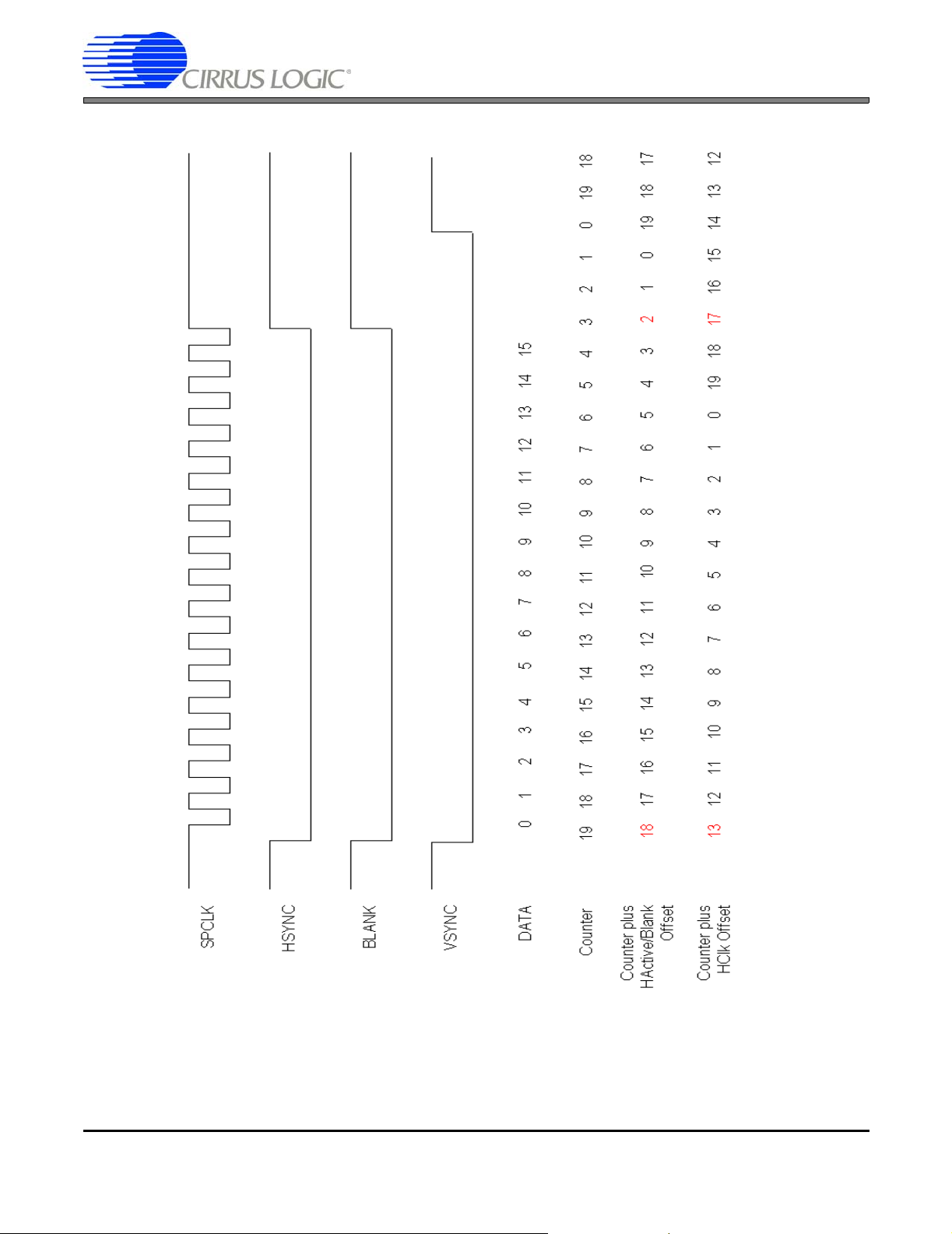
4.1.1 Horizontal and Vertical Offset Example
Given the following:
Screen Width = 16 Pixels
Screen Height = 1 Line
Screen Resolution = 16 bpp, 565.
Total Number of Horizontal Clocks = 20
Two Lines in the vertical direction
The Start of HSync signal,Blank and Vsync signal and start of data coming out must line up.
AN269REV1 5
Page 6
AN269
Figure 2. Offset for HSync, HActive, VSync and HCLK
HSync and Blank must be raised high after the last byte of data is transferred.
Find the register values for HClksTotal, HSyncStart, HSyncStop, HActiveStrt, HActiveStop, HBlankStrt,
HBlankStop, HClkStrt and HClkStop. To create these timings you must perform the following calculations.
6 AN269REV1
Page 7

The Calculations for HClksTotal are
HClksTotal = Number of Horizontal Clocks - 1
= 20 -1
= 19
The Calculations for HSyncStart are
HSyncStart = HClksTotal + Offset of Sync
= 19 + 0
= 19
TheCalculations for HSyncStop are
HSyncStop = HClksTotal - Screen Width + Offset of Sync
= 19 - 16 + 0
= 3
TheCalculations for HActiveStrt are
AN269
HActiveStrt = HClksTotal + Offset of HActive
= 19 -1
= 18
The Calculations for HActiveStop are
HActiveStop = HClksTotal - Screen Width + Offset of HActive
= 19 - 16 -1
= 2
The Calculations for HBlankStrt are
HBlankStrt = HClksTotal + Offset of HActive
= 19 -1
= 18
The Calculations for HBlankStop are
HBlankStop = HClksTotal - Screen Width + Offset of HActive
= 19 - 16 -1
= 2
AN269REV1 7
Page 8

AN269
The Calculations for HClkStrt are
HClkStrt = HClkstotal - Offset of HClk
= 19 - 6
= 13
The Calculations for HClkStop are
HClkStop = HClksTotal - Screen Width + Offset of HClk
= 19 - 16 - 6
= -3
Since -3 is not in the range of 0 and HClksTotal, add the number of Horizontal Clocks.
= -3 + Number of Horizontal Clocks
= -3 + 20
HClkStop = 17
The values for HSyncStart, HSyncStop, HActiveStrt, HActiveStop, HBlankStrt, HBlankStop, HClkStrt and
HClkStop are shown in Figure 2.
8 AN269REV1
Page 9

AN269
5. GENERAL DESCRIPTION OF PIXEL OUTPUT MODES
Each display type specifies the number of bits (and therefore bits per color) clocked out per SPCLK period. The
EP93xx supports a variety of formats, as specified in the “Output Shift Mode Table” an d “Color Mode Definition Ta-
ble” in the PixelMode register (refer to the Raster Engine chapter in the EP93xx User’s Guide for these tables).
Certain restrictions apply to these settings (as certain m odes must be used together). These restrictions, along with
the appropriate pins, are located in the table entitled “Output Pixel Transfer Modes” (again refer to the EP93xx Ras-
ter Engine chapter).
To use the “Output Pixel Transfer Modes” table, locate the output mode that corresponds to the display that is being
used. For both monochrome and color displays, the bits with highest significance should be attached to the display.
For example, if the output mode offers bits 7, 6, and 5, but the display only allows a single bit for each color, then
bit 7 should be chosen from each color. For monochrome displays, consecutive pixels should be chosen from the
same color. This will ensure that the grayscale look-up tables function as expected, as each LUT performs operations on a single color.
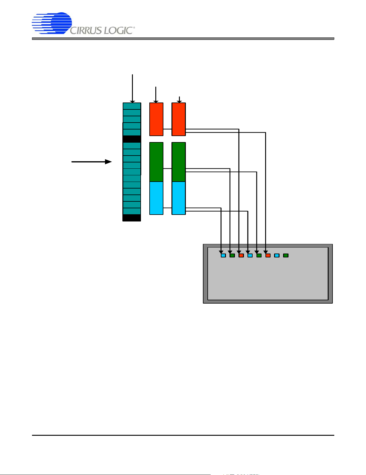
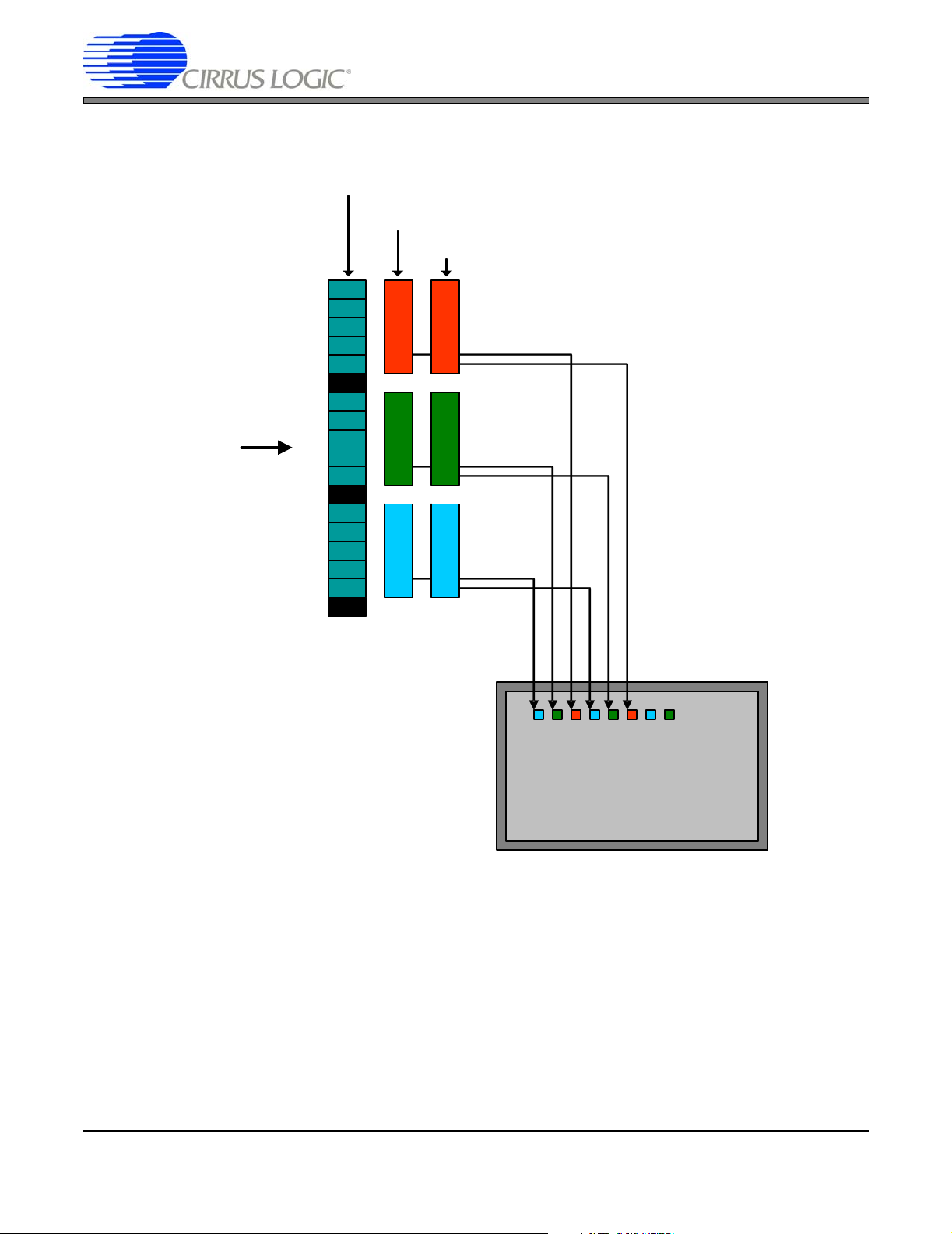
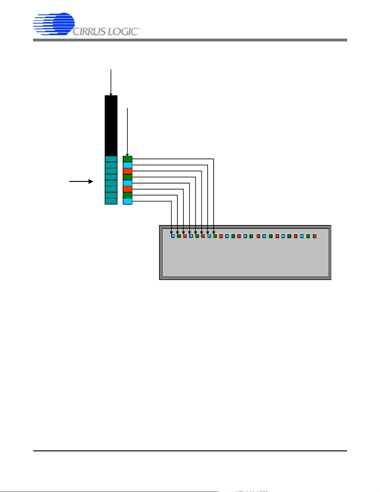
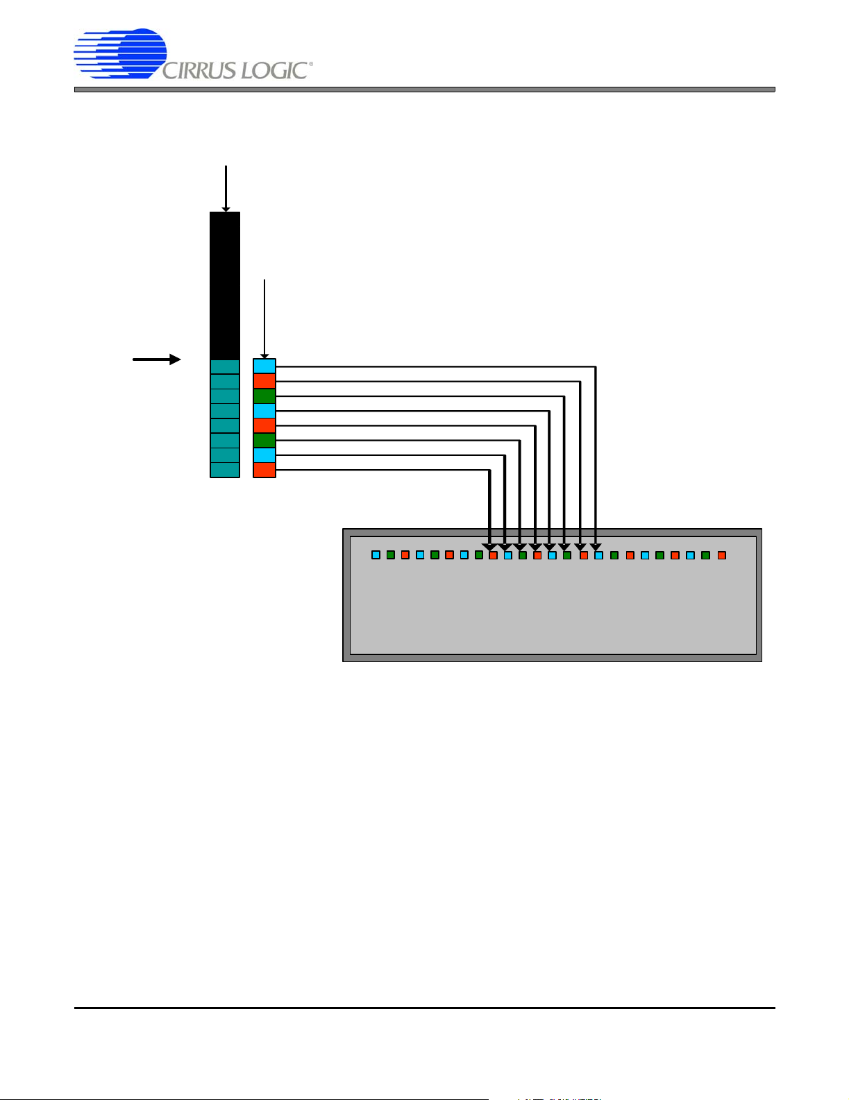
Some of the more common output modes are listed in the following diagrams, detailing where the pixel outputs end
up on the display and which corresponding pins are used for each color. These diagrams are most helpful wh en
viewed in color. A brief description of the mode follows each diagram. The input to these diagrams would be the
most-significant bits from the color and/or grayscale LUTs and the pixel MUX. Again, for monochrome displays, a
single color output (Red, Green, or Blue) should be used to ensure proper output.
Note that these diagrams are only a graphical representation of the information from the “Output Pixel Transfer
Modes” table in the Raster Engine chapter in the EP93xx User’s Guid e. Unused or redu ndant output pins ar e those
specified with gray text and a black background.
AN269REV1 9
Page 10
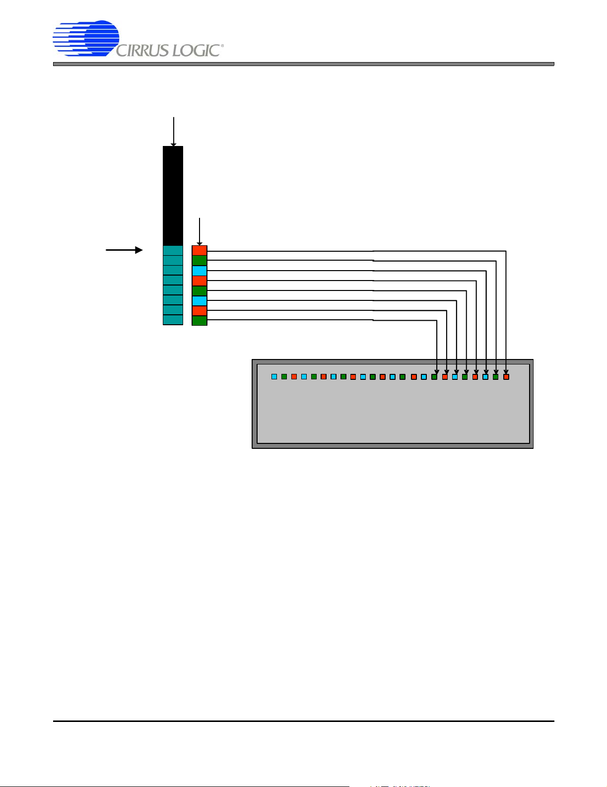
P ixel D ata B u s
Pins P[17:0]
Pixel 0 (First SPCLK)
Pixel Data Most Significant Bits
(from LUT and Blink Logic)
17
16
15
14
13
12
11
10
9
8
7
6
5
4
3
2
1
0
Pixel 1 (Second SPCLK)
0
0
0
1
1
1
AN269
Figure 3. Single 16-bit 565 Pixel Per Clock Output
The output mode “Single 16-bit 565 Pixel Per Clock” is shown in Figure 3. In this mode, each SPCLK will clock out
a single pixel, with 5 bits representing the Blue component on P[5:1], the Red component on P[17:13], and 6 bits
representing the Green component on P[11:6].
10 AN269REV1
Page 11
Pixel Data Bus
Pins P[17:0]
Pixel 0 (First SPCLK)
AN269
Pixel 1 (Second SPCLK)
Pixel Data Most Significant Bits
(from LUT and Blink Logic)
17
16
15
14
13
12
11
10
9
8
7
6
5
4
3
2
1
0
0
1
0
1
0
1
Figure 4. Single 16-bit 555 Pixel Per Clock Output
The output mode “Single 16-bit 555 Pixel Per Clock” is shown in Figure 4. In this mode, each SPCLK will clock out
a single pixel, with 5 bits representing the Blue component on P[5:1], Green component on P[11:7], and Red component of the pixel on P[17:13].
AN269REV1 11
Page 12
(from LUT and Blink Logic)
Pixel Data Most Significant Bits
Pixel Data Bus
Pins P[17:0]
17
16
Pixels 0, 1, and 2 (First SPCLK)
15
14
13
12
11
10
9
8
7
2
6
2
5
1
4
1
3
1
2
0
1
0
0
0
AN269
Figure 5. 3 Bit Per Pixel Formatted as 2-2/3 Bits, First SPCLK
The output mode “2-2/3 Pixels Per Cloc k” is shown in Figures 5, 6, and 7. Since this mode is rather complex, one
diagram shows data during each of the first, second, and third SPCLK outputs. In this mode, each SPCLK will clock
out 2-2/3 pixels, with 1 bit representing the Red, Green, and Blue components of the pixel.
In the first SPCLK, pixel 0’s Red, Green, and Blue comp onents are clocked o ut of P[2:0]. Pixel 1’s Red , Green, and
Blue components are clocked out of P[5:3]. Note that ONLY the Blue and Green component of Pixel 2 are clocked
out of P[7:6]. The Red component of pixel 2 will be clocked out during the second SPCLK.
12 AN269REV1
Page 13
Pixel Data Bus
Pins P[17:0]
1
Pixel Data Most Significant Bits
(from LUT and Blink Logic)
1
7
1
6
1
5
Pixels 2, 3, 4 and 5 (Second SPCLK)
1
4
1
3
1
2
1
1
0
9
8
5
7
4
6
5
4
4
4
3
3
2
3
1
3
0
2
AN269
Figure 6. 3-Bit Per Pixel Formatted as 2 2/3 Bits, Second SPCLK
In the second SPCLK for 2-2/3 mode, pixel 2’s Red component will be clocked out of P[0]. All of the Red, Green,
and Blue components of pixel 3 are clocked out of P[3:1]. Pixel 4’s Red, Green, and Blue components are clocked
out of P[6:4]. Note that ONLY the Blue component of Pixel 5 is clocked out of P[7]. The Green and Red components
of pixel 5 will be clocked out during the third SPCLK.
AN269REV1 13
Page 14
AN269
Pixel Data Bus
Pins P[17:0]
17
16
15
Pixel Data Most Significant Bits
(from LUT and Blink Logic)
14
13
12
Pixels 5, 6 and 7 (Third SPCLK)
11
10
9
8
7
7
6
7
5
7
4
6
3
6
2
6
1
5
0
5
Figure 7. 3-Bits Per Pixel Formatted as 2-2/3 Bits, Third SPCLK
In the third SPCLK for 2 2/3 mode, pixel 5’s Green and Red comp onents will be clocked out of P[1:0 ]. All of the Red,
Green, and Blue components of pixel 6 are clocked out of P[4:2]. Pixel 7’s Red, Green, and Blue components are
clocked out of P[7:5]. On successive SPCLK periods, the pattern of pixels will repeat.
14 AN269REV1
Page 15
AN269
Pixel Data Bus
Pins P[17:0]
Pixels 0, 1, 2 and 3
17
16
Pixel Data Most Significant Bits
(from LUT and Blink Logic)
15
14
13
12
11
10
3
3
3
3
2
2
9
2
8
2
7
1
6
1
5
1
4
1
3
0
2
0
1
0
0
0
Figure 8. 4 Pixels Per Shift Clock
In “4 Pixels-Per-Shift-Clock mode“, shown in Figure 8, only 1 bit (the MSB) will be available for the Blue and Green
components of the pixel. The Red component will have the two MSBs available. In this mode, there are 4 pixels
clocked during each SPCLK. As can be seen from the diagram, pixel 0 is outp ut on P[3:0], pixel 1 is output on P[7:4],
pixel 2 is output on P[11:8], and pixel 3 is output on P[15:12]. Note that the diagram does not show bit 6 (the secondmost-significant bit) for the Red component connected to the display, as most displays will only be using 1 bit for
each color in this mode.
AN269REV1 15
Page 16

6. SETTING UP DISPLAY TIMING
6.1 HSYNC/VSYNC-Style Displays
In displays using a HSYNC/VSYNC-style timing interface, the following control signals are commonly used
for data synchronization:
– DCLK - Data Input Clock. Usually one rising/falling edge occurs per pixel or set of pixel data. This is
the highest frequency interface signal, and transitions occur many times during each horizontal line.
– DE - Data Enable or Valid. Used to indicate valid data is currently being clocked into the display.
This may be referred to as a blanking signal, and will become active one time per valid line.
– VSYNC - Vertical Synchronization Signal. Indicates the beginning of a full frame of data. This signal
becomes active one time during one frame if in progressive mode, or two times per frame in
interlaced mode.
– HSYNC - Horizontal Synchronization Signal. Indicates the beginning of the next horizontal line. This
signal becomes active one time during the line, and many times per frame.
These signals should be connected to the EP93xx with the signal mapping shown in Table 3. Note that level
buffers may be required to meet the electrical specifications of the display.
Display Pin EP93xx Pin
AN269
DCLK SPCLK
DE BLANK
VSYNC VCSYNC
HSYNC HSYNC
Table 3. HSYNC/VSYNC Pin Mapping
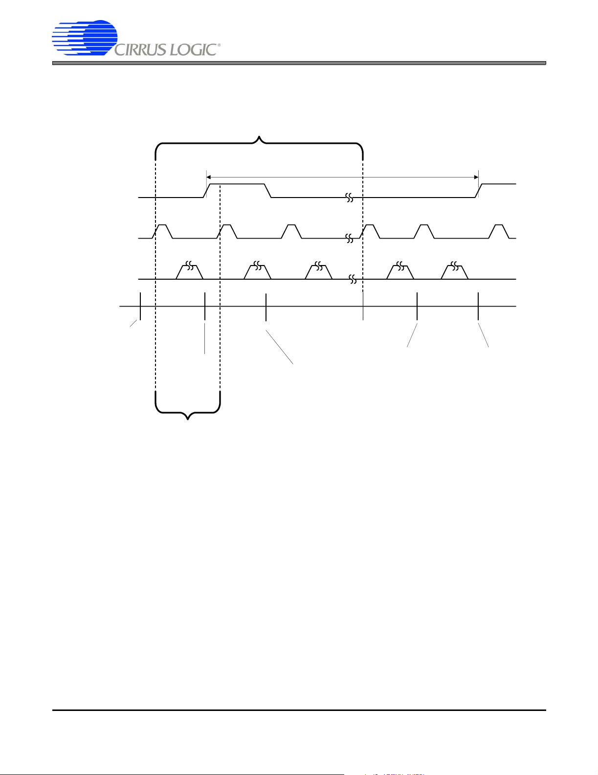
An example set of timings for an HSYNC/VSYNC-style display is shown in Figure 9. The signal names used
are those of the corresponding EP93xx pins.
16 AN269REV1
Page 17
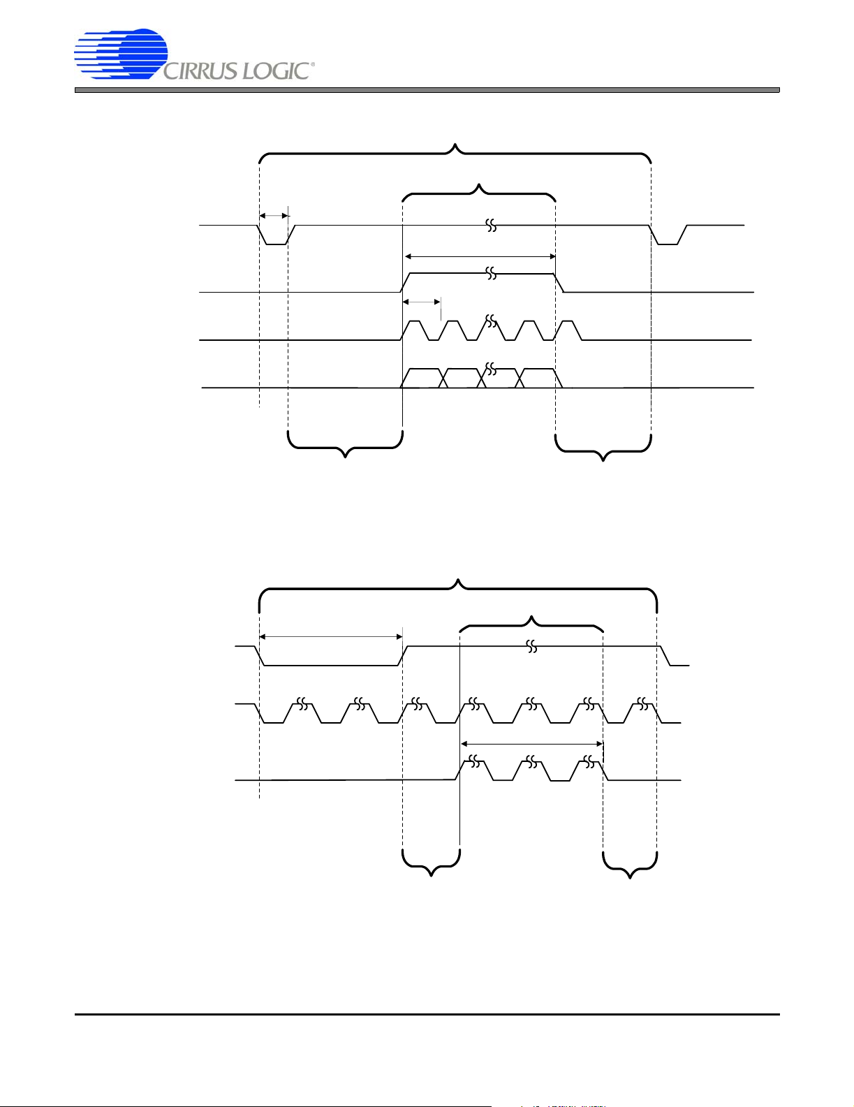
HSYNC
BLANK
SPCLK
DATA
t
HSYNC
Single Horizontal Line
Active Video
t
DCLK
t
HACTIVE
AN269
VCSYNC
HSYNC
BLANK
Back Porch Interval t
HBACKPORCH
t
Single Video Frame
VSYNC
Front Porch Interval t
Active Video
HFRONTPORCH
t
VACTIVE
Back Porch Interval t
VBACKPORCH
Front Porch Interval t
VFRONTPORCH
Figure 9. Example Timings for an HSYNC/VSYNC-Style Display
AN269REV1 17
Page 18

6.1.1 Pixel Data Clock Rate and HClkTotal/VLinesTotal
The pixel clock rate VIDCLK can be determined from the total number of VIDCLK periods per line, total
number of horizontal lines, and the Refresh Rate .
The timing specifications for this type of display interface will usually list an HSYNC Width, Horizontal
Back Porch Width, Horizontal Front Porch Width, Horizontal Valid, Horizontal B lank length, VCSYNC
Width, VCSYNC frequency, Vertical Back Porch Width, Vertical Front Porch Width, Vertical Valid, and
Vertical Blank lengths.
A typical horizontal line for this type of display can be found in Figure 10. This line can be divided into
regions, which are in units of VIDCLK. The total number of VIDCLK periods per line is the sum of the Horizontal Valid (tHACTIVE) region, the Horizontal Front Porch region (tHFRONTPORCH), the HSYNC region (tHSYNC), and the Horizontal Back Porch region (tHBACKPORCH). The equation for this is shown
here, where tHORIZ represents the number of VIDCLK periods per horizontal line (all values are in VIDCLK periods):
tHORIZ = tHACTIVE + tHFRONTPORCH + tHSYNC + tHBACKPORCH
Note that there may be 1, 2, 4, 8, or 2-2/3 pixels per SPCLK. This will mean that tHACTIVE is not necessarily the number of horizontal pixels on the screen. Con sult the datasheet o f the display to dete rmine the
number of pixels per SPCLK per horizontal line. “Genera tion of the Vide o Clock, VIDCLK” o n page 2 has
examples of the number of pixels per SPCLK (VIDCLKs/pixel is usually 1).
AN269
A typical full video frame for this type of display can be found in Figure 12. The time spent on a single
frame is the sum of the Vertical Valid (tVACTIVE) region, the Vertical Front Porch Width (tVFRONTPORCH), the VCSYNC Width (tVSYNC), and the Vertical Back Porch Width (tVBACKPORCH). The
equation for this is shown here, where tVERT represen ts the amount of time spent per single video frame
(all time is in horizontal line periods):
tVERT = tVACTIVE + tVFRONTPORCH + tVSYNC + tVBACKPORCH
Next, the specification for the refresh ra te sho uld b e dete rmined from the da tash eet. This may b e spec ified as VCSYNC or VSYNC frequency. We will call this value fVSYNC.
Now the VIDCLK rate can be determined as a product of the above 3 values. This is shown below, where
VIDCLK refers to the VIDCLK rate (Hz):
VIDCLK = tHORIZ * tVERT * fVSYNC
To generate the proper frequency for VIDCLK, either PLL1, PLL2, or an external clock must be used. Any
of these sources may be divided down using the settings in the VidClkDiv (Video Clock Divider) register.
A simple block diagram of this divide structure and a method for determining the proper settings of
VidClkDiv can be found in “Generation of the Video Clock, VIDCLK” on page 2.
Once the VIDCLK rate has been determined, the horizontal and vertical alignment signals ca n be derived.
18 AN269REV1
Page 19
6.1.2 Horizontal Alignment Signals
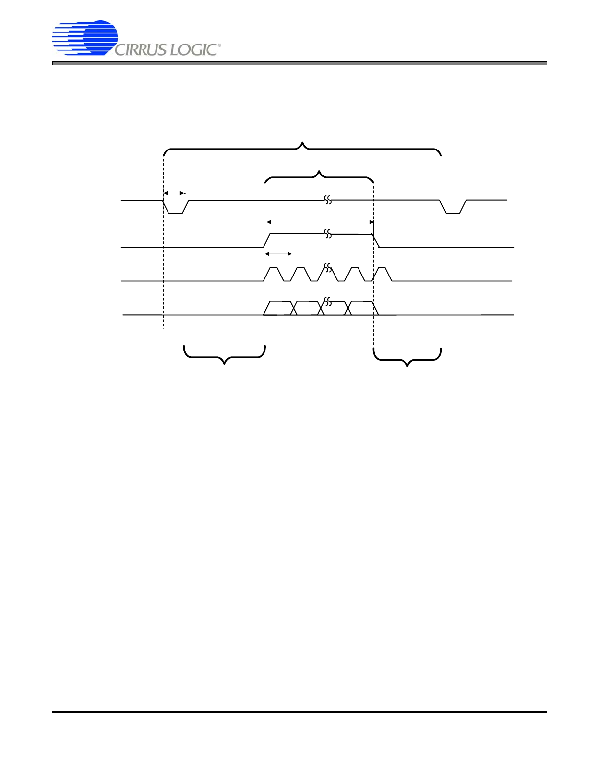
Timings for a single horizontal line can be seen in Figure 10. To determine when these signals become
active, the horizontal frame timing registers HClkTotal, HSyncStrtStop, HActiveStrtStop, HBlankStrtStop
and HClkStrtStop must be set.
t
HSYNC
HSYNC
BLANK
SPCLK
DATA
Single Horizontal Line
Active Video
t
DCLK
t
HACTIVE
AN269
Back Porch Interval t
HBACKPORCH
Front Porch Interval t
HFRONTPORCH
Figure 10. Typical Horizontal Line for HSYNC/VSYNC Display
“Using the Horizontal and Vertical Counter for Timing-Signal Generation” on page 4 for a description o f
the horizontal timing registers.
Recall that the timing specifications for this type of display interface will list an HSYNC Width, Horizontal
Back Porch Width, Horizontal Front Porch Width, Horizontal Valid, and Horizontal Blank lengths.
The HClkTotal register will hold the total length of a single line measured in VIDCLK periods.The equation
for this is shown here:
HClkTotal = tHORIZ – 1
Note that 1 is subtracted for the total as this is a 0-based counte r implementation. Also, remember all measurements are assumed to be in periods of VIDCLK. All other signals are determined using this as a time
base.
To determine when the HSYNC, SPCLK (via HCLKEN), and BLANK (via HBLANK) signals should become active during a horizontal line, it is easiest to draw them out as shown in Figure 11. This diagram
shows the line counter along the bottom , starting at HClkTotal and cou nting down to 0. Each line start s
with the counter set to HClkTotal. It then decrements by 1 for each VIDCLK clock period, regardless of
whether SPCLK is present or not. When the counter reaches 0, it is reset to HClkTotal.
AN269REV1 19
Page 20

Single Horizontal Line
Active Video
t
HSYNC
HSYNC
t
HACTIVE
BLANK
t
DCLK
SPCLK
DATA
HSyncStop
HSyncStart
Horizontal Line
Counter Value
Count = HClkTotal Count = 0
Count = HClkTotal - 1
Count = HClkTotal - 2
HSyncStop
HBlankStart
HActiveStart
HBlankStop
HActiveStop
AN269
Back Porch Interval t
HBACKPORCH
Front Porch Interval t
HFRONTPORCH
Figure 11. Horizontal Line for HSYNC/VSYNC Display with Register Timings
Next we will determine the appropriate time for the HSYNC signal to become active. As can be seen from
the diagram, it should become active during the tHSYNC region, when the line counter is set to HClkTotal
(the beginning of the horizontal line). HSYNC becomes inactive after a period of time tHSYNC has
elapsed. Therefore, the HSYNC signa l should become inactive after the tHSYNC region, when the line
counter is HClkTotal-tHSYNC. This is shown using the equations below, where HSyncStart is the point at
which HSYNC becomes active and HSyncStop is the point at which HSYNC becomes inactive:
HSyncStart = HClkTotal
HSyncStop = HClkTotal – tHSYNC
The active data/blank signal HBLANK becomes inactive when valid data starts, and active once the vali d
data stops. In other words, the HBLANK signal should be active for all regions except the active region
(tACTIVE). Therefore, when the h orizontal line counter reaches the end of the ba ck porch interval, it
should become inactive. At the beginning of the front porch interval, it should become active again. The
following equations show this, using HBlankStart as the position at which this signal becomes active, and
HBlankStop as the position at which this signal becomes inactive (note that HBlankStop is 1 less than the
front porch, as this is a 0-based counter implementation):
HBlankStart = HClkTotal - tHSYNC - tHBACKPORCH -1
HBlankStop = tHFRONTPORCH - 1
20 AN269REV1
Page 21

AN269
The next two values of interest for a horizon tal line are the times at which active data s hould be cl ocked
out. These values determine when valid data is presented to the display. As can be seen from the diagram, those times are identical to the locations at which the active data/blank signal are changing (the
active region or tACTIVE). The formulas below calculate HActiveStart as the start of active data and HActiveStop as the end of active data. The offset of minus one comes from Table 2.
HActiveStart = HClkTotal - tHSYNC - tHBACKPORCH - 1
HActiveStop = tHFRONTPORCH - 1
If clock gating is not required, the HClkStart may be set to HCLKSTOTAL and HClkStop can be set to
HClkTotal + 1 . The counter and HCLKSTOP values are never equal so the clock never stops.
HClkStart = HClkTotal
HClkStop = HClkTotal + 1
When clock gating is required, the SPCLK signal is seen at the output when the horizontal pixel counter
is in the active range HClkStart > horizontal pixel counter > HClkStop. The appropriate values should be
identical to the HBlankStart, and HBlankStop values with the offset of minus six.
HClkStart = HClkTotal - tHSYNC - tHBACKPORCH - 6
HClkStop = tHFRONTPORCH - 6
The above values must then be shifted properly and assigned to the HClkTotal, HSyncStrtStop, HActiveStrtStop, HBlankStrtStop, and HClkStrtStop registers.
See “Example HSYNC/VSYNC-Style LCD Display - LB/Philips LB064V02-B1” on page 52 for an example
calculation for this type of display
AN269REV1 21
Page 22

6.1.3 Vertical Alignment Signals
Timings for a single vertical frame can be seen in Figure 12. The tim in g of the sync hr on iza tio n sig na ls is
determined by the vertical frame timing registers VLinesTotal, VSyncStrtStop, VActiveStrtStop, VBlankStrtStop, and VClkStrtStop.
VCSYNC
HSYNC
BLANK
Single Video Frame
t
VSYNC
Active Video
t
VACTIVE
AN269
Back Porch Interval t
Figure 12. HSYNC/VSYNC Video Frame
VBACKPORCH
Front Porch Interval t
VFRONTPORCH
See “Using the Horizontal and Vertical Co unter for Timing-Signal Gener ation” on page 4 for a description
of the vertical timing registers.
Recall from above that the timing specifications for this type of display interface will list a VCSYNC Width,
Vertical Back Porch Width, Vertical Front Porch Width, Vertical Valid, and Vertical Blank lengths.
The VLinesTotal register will hold the total length of a single frame measured in horizontal lines. It is the
sum of the Vertical Valid (tVACTIVE) region, the Vertical Front Porch Width (tVFRONTPORCH), the VCSYNC Width (tVSYNC), and the Vertical Back Porch Width (tVBACKPORCH). The equation for this is
shown here (tVERT is calculated in Section 6.1.1):
VLinesTotal = tVERT – 1
Note that 1 is subtracted for the total as this is a 0-based counter implementation. Also, all measurements
are assumed to be in periods of horizontal lines. All other signals are determined using th is as a time base.
To determine when the VCSYNC, BLANK, and SPCLK signals should become active during a frame, it
is easiest to draw them out as shown in Figure 13. This diagram shows the line counter along the bottom,
starting at VLinesTotal and counting down to 0. Each frame starts with the counter set to VLinesTotal. It
22 AN269REV1
Page 23

AN269
then counts down by 1 for each HSYNC time period, regardless of whether SPCLK/DATA is present or
not. When the counter reaches 0, it is reset to VLinesTotal.
Single Video Frame
Active Video
t
VSYNC
VCSYNC
HSYNC
t
VACTIVE
BLANK
Vertical Line
Counter Value
Count = VLinesTotal
Count = VLinesTotal - 1
Count = VLinesTotal - 2
Back Porch Interval t
Figure 13. HSYNC/VSYNC Video Frame with Register Timing
VBACKPORCH
Front Porch Interval t
Count =0
VFRONTPORCH
Next we will determine the appropriate time for the VCSYNC signal to become active. As can be seen
from the diagram, VCSYNC becomes active when the line counter is reset to VLinesTo ta l (the b eginnin g
of the frame). VCSYNC becomes inactive after the period of tVSYNC has elapsed. Therefore, the VSYNC
signal should become inactive when the line counter is VLinesTotal-tVSYNC. This is shown using the
equations below, where VSyncStart is the point at which VCSYNC becomes a ctive and VSyncStop is th e
point at which VCSYNC becomes inactive (again, all time is measured in horizontal line periods):
VSyncStart = VLinesTotal
VSyncStop = VLinesTotal – tVSYNC
The active data/blank signal becomes active when valid data starts, and inactive once the valid data
stops. Therefore, when the vertic al line counte r reach es the end o f the bac k porch in terval, it sh ould be come active. At the beginning of the front porch interval, it should become inactive. The following equations show this, using VBlankStart as the position at which this signal becomes active, and VBlankStop
as the position at which this signal becomes inactive (VBlankStop is 1 less than tVFRONTPORCH due to
0-based counter implementation):
VBlankStart = VLinesTotal - tVSYNC - tVBACKPORCH
VBlankStop = tVFRONTPORCH - 1
AN269REV1 23
Page 24

AN269
The next two values of interest for a frame are the point at which active da ta should be clocked out. These
values determine when valid data is presen ted to the display. As can be seen fr om the diagram, those
times are identical to the locations at which the active data /blank signal are ch anging. Using VActiveStart
as the start of active data and VActiveStop as the end of active data:
VActiveSt art = VBlankStart
VActiveStop = VBlankStop
The last two values that must be determined are the VClkStart and VClkStop values. These determine
when the SPCLK signal is seen at the output during the full video frame. In situations where clock gating
is not required, these may be set such that SPCLK is always running:
VClkStart = VLinesTotal
VClkStop = VLinesTotal
When clock gating is required, the SPCLK signal is seen at the output when the line counter is in the active
range VClkStart > line counter > VClkStop. If the clock should only be present during valid horizontal lines,
the appropriate values should be assigned as such:
VClkStart = VActiveStart
VClkStop = VActiveStop
The above values must then be shifted properly and assigne d to the VLinesTota l, VSyncStrtStop, VActiveStrtStop, VBlankStrtStop, and VClkStrtStop registers.
For an example calculation for this type of display, see “Example HSYNC/VSYNC-Style LCD Display -
LB/Philips LB064V02-B1” on page 52.
6.2 Framed Data Style Displays - Type 1
In displays using a framed data style timing interface, the following control signals are commonly used for
data synchronization:
– CP - Data Input Pixel Clock. Usually one rising/falling edge occurs per pixel or set of pixel data. This
is the highest frequency interface signal, and transitions occur many times during each horizontal
line, once for each horizontal pixel.
– FRM - Vertical Synchronization or Frame Signal. Indicates the beginnin g of a full frame of data. Th is
signal becomes active one time during a single video frame.
– LOAD - Horizontal Synchronization or Load Signal. Indicates the beginning of the next horizontal
line. This signal becomes active one time during the line, and many times per full video frame.
These signals should be connected to the EP93xx with the signal mapping shown in Table 4.
24 AN269REV1
Page 25

AN269
Display Pin EP93xx Pin
CP SPCLK
FRM VCSYNC
LOAD HSYNC
Table 4. Frame Type 1 Pin Mapping
A timing diagram for this type of display is shown in Figure14. Signal and timing names are those of the
corresponding EP93xx pins. A description of the timing requirements is given in Table 5
Timing Parameter Description
tHSYNCH HSYNC High pulse duration
tHSYNCSPCLK Time from HSYNC Low to first SPCLK on this line
tSPCLKHSYNC Time from last SPCLK to HSYNC High on next line
tHVCSYNC Time from HSYNC Low to VCSYNC High
tVCHSYNC Time from VCSYNC High to HSYNC Falling Edge
tSPCLKHSYNC Time from the last SPCLK to HSYNC Rising Edge
Table 5. Frame Type 1 Relevant Timing Parameters
In this type of display, the total number of SPCLKs per horizontal line is equal to the horizontal resolution.
Also, the total number of SPCLKs per full video frame is the horizontal resolution times the vertical resolution. Unlike an HSYNC/VSYNC-style display, there are no “extra” HSYNC or SPCLK pulses in the frame.
This will be accomplished by using a gated SPCLK, controlled by the HClkStrtStop register.
Note that in this timing, the VCSYNC signal actually comes after the HSYNC signal. To accomplish this, the
horizontal line counter is aligned such that line transitions occur at the VCSYNC transitions. This will be illustrated in greater detail when the horizontal and vertical timings are determined.
AN269REV1 25
Page 26

HSYNC
SPCLK
DATA
VCSYNC
(Horizontal
Line 1 ONLY)
t
HVCSYNC
t
HSYNCH
t
HSYNCL
t
HSYNCSPCLK
t
VCHSYNC
Single Horizontal Line
t
SPCLK
t
SPCLKHSYNC
AN269
VCSYNC
HSYNC
SPCLK
First Line
One SPCLK per Horizontal Pixel
Single Video Frame
t
VCSYNC
Figure 14. Frame Type 1 Display Timing
26 AN269REV1
Page 27

6.2.1 VIDCLK and Pixel Data Clock Rate
For Frame Type 1 data displays, the SPCLK will be gated such that clock pulses only occur during valid
data, one pulse per data set. Note that the numbe r of pixels pe r SPCLK may be 1 , 2, 2-2/3, 4, or 8. Also,
the number of VIDCLK periods per SPCLK may not always be constant. For exam ple, in 2 2/3 mode, there
are 3, 2, and then 3 VIDCLKs per SPCLK (thus an average of (3+2+3 VIDCLKs/SPCLK) with (2-2/3 pixels/SPCLK) = 1 VIDCLK/pixel).
To determine the VIDCLK rate (and therefore the resulting SPCLK rate), the number of SPCLK s per h orizontal line must be estimated. This is done by identifying the different regions of the horizontal line and
assigning a certain number of VIDCL Ks to that region. This method is a bit complex due to the fact that
adding VIDCLKs per line will inherently increase the overall VIDCLK (and therefore SPCLK) frequency.
However, a simple iterative process can be used to determine the proper rates.
To simplify the example, we are only going to use the following timing parameters, which will later be used
as regions of time on the horizontal line (the regions will be discussed in depth later in this chapter):
– tHSYNCH - Time for HSYNC high.
– tHVCSYNC - Time from HSYNC low to VCSYNC high.
– tSPCLKHSYNC - Time from last SPCLK until HSYNC high.
– tHSYNCSPCLK - Time from HSYNC low until first SPCLK for this line.
– tACTIVE - The period of the actual active region itself.
AN269
The first step is to estimate the VIDCLK rate. This is done with the following formula:
DesiredVidClkFreq = {(VIDCLKs per Pixel * Horizontal Resolution) + [(2 SPCLKs for each reg ion)*(4 regions not including the active region)]} * (Vertical Resolution) * (Desired Refresh Rate)
The quantity of VIDCLKs per Pixel (VIDCLKs per Pixel) depends on the operating mode, but is usually 1.
Note that we have estimated 2 SPCLKs for each regi on, for each of the 4 regions: HSYNC high, HSYNC
until VCSYNC, VCSYNC until first SPCLK, and last SPCLK until the next line’s HSYNC high.
The next step involves setting up the VIDCLKDIV register, and determining the actual “nearest” value of
VIDCLK frequency. This will not necessarily be the desired VIDCLK frequency, but will be close. An algorithm for this is shown in Section 3. “Generation of the Video Clock, VIDCLK” on page 2. The value returned by setting the VIDCLKDIV register is the actual frequency of VIDCLK (the quantity
ActualVidClkFreq). From the value of ActualVidClkFreq, the VIDCLK period can be determined (the quantity VidClkPeriod):
VidClkPeriod = 1 / ActualVidClkFreq
6.2.2 Horizontal Alignment Signals
To determine the length of time spent on a single horizontal line, the refresh rate is multiplied by the vertical resolution and inverted (1/X), yielding the value LinePeriod:
LinePeriod = 1 / [(refresh rate) * (vertical resolution)]
From that, the number of VIDCLK periods per line (NumVideoClocks) is:
NumVideoClocks = LinePeriod/VidClkPeriod
AN269REV1 27
Page 28

AN269
Note that the number of available video clocks can also be derived by adding up the number of clocks in
each region, but this approach will guarantee a more accurate line frequency.
The value of NumVideoClocks will be the total number of “available” VIDCLK periods for each region of
time in the horizontal line. In order to visualize th is quantity, see Figure 15. Note that the NumVideoClocks
quantity represents the total number of VIDCLKs per horizontal line, and therefore will be HClksTotal+1.
Single Horizontal Line
t
HSYNCH
t
HSYNCL
HSYNC
t
SPCLK
DATA
VCSYNC
(Horizontal
Line 1 ONLY)
Horizontal Line
Counter Value
HSyncStart
t
HVCSYNC
t
HSYNCSPCLK
t
VCHSYNC
HSyncStop
HSyncStop
SPCLK
HActiveStart
t
SPCLKHSYNC
HActiveStop
Count = 0
Count = HClkTotal
Count = HClkTotal - 1
Count = HClkTotal - 2
One SPCLK per Horizontal Pixel
Count = 0
Count = HClkTotal
Figure 15. Horizontal Line for Frame Type 1 Displays
Now, the number of VIDCLK periods required for the active region (i.e., region with valid pixel data) can
be determined. In the following equation, ActiveVidClks represents the total number of VIDCLKs that will
occur while outputting pixel data (VIDCLKs per Pixel is usually 1):
ActiveVidClks = (VIDCLKs per Pixel) * (horizontal resolution)
We will now discuss each of the regions in more detail. Each region is labeled by the appropriate length
of time, in VIDCLKs. A diagram of this is shown in Figure 16. The time from the HSYNC signal becoming
active to the time it becomes inactive is LoadHighVidClks. The time from the HSYNC signal becoming
inactive until the VCSYNC signal becomes active (on the first frame) is noted as FrameHoldVidClks. The
time from VCSYNC becoming active until the first valid SPCLK is LoadCPVidClks. The time from the last
SPCLK until the next HSYNC is CPLoadVidClks.
28 AN269REV1
Page 29

AN269
.
Single Horizontal Line
t
HSYNCH
t
HSYNCL
HSYNC
t
SPCLK
DATA
VCSYNC
(Horizontal
Line 1 ONLY)
Horizontal Line
Counter Value
HSyncStart
t
HVCSYNC
t
HSYNCSPCLK
t
VCHSYNC
HSyncStop
SPCLK
HActiveStart
t
SPCLKHSYNC
HActiveStop
Count = 0
Count = HClkTotal
Count = HClkTotal - 1
Count = HClkTotal - 2
One SPCLK per Horizontal Pixel
LoadHighVidClks
FrameHoldVidClks
LoadCPVidClks
ActiveVidClks
Figure 16. Frame Type 1 Display with Colored Regions
CPLoadVidClks
AN269REV1 29
Page 30

AN269
Since the remaining region widths are determine d by their re spective timing para meter s, here are so me
equations to determine the number of VIDCLK periods required for the displa y:
LoadHighVidClks = (tHSYNCH / VidClkPeriod) + 1
FrameHoldVidClks = (tHVCSYNC / VidClkPeriod) + 1
LoadCPVidClks = [(tHSYNCSPCLK - tHVCSYNC) / VidClkPeriod] + 1
CPLoadVidClks = (tSPCLKHSYNC / VidClkPeriod) + 1
Note that 1 is added to the result to round up, and tHSYNCH, tHVCSYNC, etc. are in units of seconds.
Once we have these quantities, the number of remaining VIDCLKs per line (those not needed by any region) is found by subtracting all of the above quantities from the number of available VIDCLKs per horizontal line:
AvailableVidClks = NumVideoClocks - ActiveVidClks - LoadHighVidClks - FrameHoldVidClks -
LoadCPVidClks - CPLoadVidClks
If this quantity is negative, there are not enough VIDCLKs per line, and therefore the VIDCLK frequency
must be increased. To do this, go back to Section 6.2.1 and increase the number of VIDCLKs for any section that may require more and recalculate the higher VIDCLK frequency (the number of VIDCLKs may
have to be increased until the actual frequency goes up). As mentioned earlier, this will change the VIDCLK frequency, and therefore the AvailableVidClks. This process may need to be repeate d several times
until a suitable VIDCLK frequency is found.
If the AvailableVidClks is 1 or more, than these clocks can be distributed among the various regions (padding each region) until all remaining VidClks have been assigned. As each clock is distributed, update the
value of ActiveVidClks, LoadHighVidClks, FrameHoldVidClks, LoadCPVidClks, and CPLoadVidClks.
Now that each region is assigned a certain number of VIDCLK periods, determining the register values
for the EP93xx raster engine is straightforward (note offsets where appropriate due to internal delays in
the raster block):
HClksTotal = NumVideoClocks - 1
HSyncStart = LoadHighVidClks + FrameHoldVidClks - 1
HSyncStop = FrameHoldVidClks - 1
HActiveStart = HClksTotal - LoadCPVidClks -1
HActiveStop = HClksTotal - LoadCPVidClks - ActiveVidClks -1
HClksStart = HClksTotal - LoadCPVidClks - 6
HClksStop = HClksTotal - LoadCPVidClks - ActiveVidClks - 6
Note that the blank output is not used, so 0 can be assigned to the horizontal blank timing registers:
HBlankStart = 0
HBlankStop = 0
30 AN269REV1
Page 31

6.2.3 Vertical Alignment Signals
The vertical timing alignment signals are easily determined by looking at Figure 17.
VCSYNC
HSYNC
SPCLK
Vertical Line
Counter Value
Single Video Frame
t
VCSYNC
AN269
Count = VLinesTotal
Count = VLinesTotal - 1
Count = VLinesTotal - 2
First Line
Count =0
Count = VLinesTotal
Figure 17. Frame Type 1 Display Vertical Timing
The total number of lines is equal to the vertical resolutio n (notice there are no “blank” lines):
VLinesTotal = (vertical resolution) - 1
The VCSYNC signal becomes active when the vertical line counter is VLinesTotal and becomes inactive
when it is VLinesTotal-1. Therefore:
VSyncStart = VLinesTotal
VSyncStop = VLinesTotal - 1
AN269REV1 31
Page 32

Another result of having no “blank” lines is that the active region covers all of the horizontal lines, so the
active region is the entire vertical width:
VActiveStart = VLinesTotal
VActiveStop = VLinesTotal + 1
VActiveStop is set this way to insure that pixel data is not stopped due to vertical position. Also, the
SPCLK should not be stopped due to vertical position:
VClkStart = VLinesTotal
VClkStop = VLinesTotal + 1
The blank signal is not used, but it may be desired to initialize the Vertical Blanking timing registers to a
known value:
VBlankStart = 0
VBlankStop = 0
6.3 Framed Data Style Displays - Type 2
AN269
In displays using a framed data style timing interface, the following control signals are commonly used for
data synchronization:
– CP - Data input pixel clock. Usually one rising/falling edge occurs per pixel or set of pixel data. This
is the highest frequency interface signal, and transitions occur many times during each horizontal
line, once for each horizontal pixel.
– FRM - Vertical Synchronization or Frame Signal. Indicates the beginnin g of a full frame of data. Th is
signal becomes active one time during a single video frame.
– LOAD - Horizontal Synchronization or Load Signal. Indicates the beginning of the next horizontal
line. This signal becomes active one time during the line, and many times per full video frame.
These signals should be connected to the EP93xx with the signal mapping shown in Table 6.
Display Pin EP93xx Pin
CP SPCLK
FRM VCSYNC
LOAD HSYNC
Table 6. Frame Type 2 Pin Mapping
32 AN269REV1
Page 33

AN269
A timing diagram for this type of display is shown in Figure18. Signal and timing names are those of the
corresponding EP93xx pins. A description of the timing requirements is given in Table 7.
Timing Parameter Description
tHSYNCH HSYNC High pulse duration
tVCHHSYNC Time from VCSYNC High to HSYNC low
tSPCLKHSYNC Time from last SPCLK to HSYNC High on next line
tHSYNCSPCLK Time from HSYNC Low to first SPCLK
tVCLHSYNC Time from VCSYNC Low to HSync Rising Edge
Table 7. Frame Type 2 Relevant Timing Parameters
In this type of display, the total number of SPCLKs per horizontal line is equal to the horizontal resolution.
Also, and the total number of SPCLKs per full video fram e is the horizontal resolutio n times the vertical resolution. Unlike an HSYNC/VSYNC-style display, there are no “extra” HSYNC or SPCLK pulses in the frame.
This will be accomplished by using a gated SPCLK, controlled by the HClkStrtStop register.
Note that in this timing, the VCSYNC signal comes before the HSYNC signal. To accomplish this, the horizontal line counter should be aligned such that the line transition occurs at the VCSYNC transitions. More
on this will be illustrated when the horizontal and vertical timings are determined.
AN269REV1 33
Page 34

HSYNC
SPCLK
DATA
t
HVCSYNC
VCSYNC
(Horizontal
Line 1 ONLY)
t
HSYNCH
Single Horizontal Line
t
HSYNCSPCLK
t
VCHHSYNC
t
SPCLKHSYNC
t
VCLHSYNC
AN269
VCSYNC
HSYNC
SPCLK
First Line
One SPCLK per Horizontal Pixel
Single Video Frame
t
VCSYNC
Figure 18. Frame Type 2 Display Timing
34 AN269REV1
Page 35

6.3.1 VIDCLK and Pixel Data Clock Rate
For a frame type 2 data display, the SPCLK will be gated such that clock pulses only occur during valid
data, one pulse per data set. Note that the numbe r of pixels pe r SPCLK may be 1 , 2, 2-2/3, 4, or 8. Also,
the number of VIDCLK periods per SPCLK may not always be constant. For example, in 2-2/3 mode,
there are 3, 2, and then 3 VIDCLKs per SPCLK (thus an average of (3+2+3 VIDCLKs/SPCLK) with (2-2/3
pixels/SPCLK) = 1 VIDCLK/pixel).
To determine the VIDCLK rate (and therefore the resulting SPCLK rate), the number of SPCLK s per h orizontal line must be estimated. This is done by identifying the different regions of the horizontal line, and
assigning a certain number of VIDCL Ks to that region. This method is a bit complex due to the fact that
adding VIDCLKs per line will inherently increase the overall VIDCLK (and therefore SPCLK) frequency.
However, a simple iterative process can be used to determine the proper rates.
To simplify the example, we are only going to use the following timing parameters, which will later be used
as regions of time on the horizontal line (the regions will be discussed in more detail later in this chapter):
– tHSYNCH - HSYNC High pulse duration
– tVCHHSYNC - Time from VCSYNC High to HSYNC low
– tSPCLKHSYNC - Time from last SPCLK to HSYNC High on next line
– tHSYNCSPCLK - Time from HSYNC Low to first SPCLK
– tVCLHSYNC - Time from VCSYNC Low to HSync Rising Edge
– tACTIVE - The period of the actual active region itself.
AN269
The first step is to estimate the VIDCLK rate. This is done with the following formula:
DesiredVidClkFreq = {[(VIDCLKs per Pixel) * (Horizontal Resolution)] + [(2 SPCLKs for each region)*(4
regions not including the active region)]} * (Vertical Resolution) * (Desired Refresh Rate)
The quantity of VIDCLKs per Pixel (VIDCLKs per Pixel) depends on the operating mode, but is usually 1.
Note that we have estimated 2 SPCLKs for each region for each of 4 regions: HSYNC high, VCSYNC until
HSYNC, HSYNC low until first SPCLK, and last SPCLK until the next line’s HSYNC high.
The next step involves setting up the VIDCLKDIV register, and determining the actual “nearest” value of
VIDCLK frequency. This will not necessarily be the desired VIDCLK frequency, but will be close. An algorithm for this is shown in Section 3. “Generation of the Video Clock, VIDCLK” on page 2. The value returned by setting the VIDCLKDIV register is the actual frequency of VIDCLK (the quantity
ActualVidClkFreq). From the value of ActualVidClkFreq, the VIDCLK period ca n be determined (the quantity VidClkPeriod):
VidClkPeriod = 1 / ActualVidClkFreq
AN269REV1 35
Page 36

6.3.2 Horizontal Alignment Signals
To determine the length of time spent on a single horizontal line, the refresh rate is multiplied by the vertical resolution, and inverted (1/X), yielding the value LinePeriod:
LinePeriod = 1 / [(refresh rate) * (vertical resolution)]
From that, the number of VIDCLK periods per line (NumVideoClocks) is:
NumVideoClocks = LinePeriod per VidClkPeriod
Note that the number of available video clocks can also be derived by adding up the number of clocks in
each region, but this approach will guarantee a more accurate line frequency.
The value of NumVideoClocks will be the total number of “available” clocks for all regions of time in the
horizontal line. In order to visualize this quantity, the see Figure 20. Note that the NumVideoClocks quantity represents the total number of VIDCLKs per horizontal line, and therefore will be HClksTotal+1.
AN269
36 AN269REV1
Page 37

HSYNC
SPCLK
DATA
t
HVCSYNC
VCSYNC
(Horizontal
Line 1 ONLY)
Horizontal Line
Counter Value
t
HSYNCH
Single Horizontal Line
t
HSYNCSPCLK
t
VCHHSYNC
HSyncStart
HActiveStart
t
SPCLKHSYNC
HActiveStop
t
VCLHSYNC
AN269
Count = 0
Count = HClkTotal
Count = HClkTotal - 1
One SPCLK per Horizontal Pixel
HSyncStop
HSyncStop
Count = 0
Count = HClkTotal
Figure 19. Horizontal Line for Frame Type 2 Displays
Now, the number of VIDCLK periods required for the active region (i.e., region with valid pixel data) can
be determined. In the following equation, ActiveVidClks represents the total number of VIDCLKs that will
occur while outputting pixel data (there is usually 1 VIDCLK per pixel):
ActiveVidClks = (VIDCLKs/Pixel) * (horizontal resolution)
We will now discuss each of the regions in more detail. Each region is labeled by the appropriate length
of time, in VIDCLKs. A diagram of this is shown in Figure 20. The time from VCSYNC signal becoming
active until the HSYNC signal becomes active (on the second line) is noted as the FrameHoldVidClks.
The time from the HSYNC signal becoming active to the time it becomes inactive is LoadHighVidClks.
The time from HSYNC becoming inactive until the first valid SPCLK is LoadCPVidClks. This will guarantee
AN269REV1 37
Page 38

AN269
that the timing is met by making the quantity larger than it needs to be. The time from the last SPCLK until
the VCSYNC signal becomes inactive (on the second line) is CPLoadVidClks.
.
Single Horizontal Line
t
HSYNC
SPCLK
DATA
VCSYNC
(Horizontal
Line 2 ONLY)
Horizontal Line
Counter Value
HSYNCH
t
HSYNCSPCLK
Count = 0
Count = HClkTotal
t
VCHHSYNC
HSyncStart
HSyncStop
Count = HClkTotal - 1
HActiveStart
Count = HClkTotal
HActiveStop
Count = 0
t
SPCLKHSYNC
t
VCLHSYNC
One SPCLK per Horizontal Pixel
LoadCPVidClks
LoadHighVidClks
FrameHoldVidClks
ActiveVidClks
CPLoadVidClks
Figure 20. Frame Type 2 Display with Colored Regions
38 AN269REV1
Page 39

AN269
Since the remaining region widths are determined by their respective timing parameters, here are some
equations to determine the number of VIDCLK periods required for the display:
LoadHighVidClks = (tVCLHSYNC / VidClkPeriod) + 1
FrameHoldVidClks = [(tVCHHSYNC - tVCLHSYNC) / VidClkPeriod] + 1
LoadCPVidClks = (tHSYNCSPCLK / VidClkPeriod) + 1
CPLoadVidClks = [(tSPCLKHSYNC - tVCLHSYNC) / VidClkPeriod] + 1
Note that 1 is added to the result to round up. Once we have these quantities, the number of remaining
VIDCLKs per line (those not needed by any region) is found by subtracting all of the above quantities from
the number of available VIDCLKs per horizontal line:
AvailableVidClks = NumVideoClocks - ActiveVidClks - LoadHighVidClks - FrameHoldVidClks -
LoadCPVidClks - CPLoadVidClks
If this quantity is negative, there are not enough VIDCLKs per line, and therefore the VIDCLK frequency
must be increased. To do this, go back to Section 6.3.1 on page 35 a nd increase the nu mber of VIDCLKs
for any region that may require more, then recalculate a higher VIDCL K frequency. As men tioned earlie r,
this will change the VIDCLK frequency, and therefore the AvailableVidClks. This process may need to be
repeated several times until a suitable VIDCLK frequency is found.
If the AvailableVidClks is 1 or more, then these clocks can be distributed among the various regions (padding each region) until all remaining VidClks have been assigned. As each clock is distributed, update the
value of ActiveVidClks, LoadHighVidClks, FrameHoldVidClks, LoadCPVidClks, and CPLoadVidClks.
Now that each region is assigned a certain number of VIDCLK periods, determining the register values
for the EP93xx Raster Engine is straightforward (delay offsets included are to compensate for internal delays in the raster engine):
HClksTotal = NumVideoClocks - 1
HSyncStrt = HClksTotal - FrameHoldVidClks
HSyncStop = HClksTotal - FrameHoldVidClks - LoadHighVidClks
HActiveStrt = ActiveVidClks + CPLoadVidClks -1
HActiveStop = CPLoadVidClks - 1
HClkStrt = ActiveVidClks + CPLoadVidClks - 6
HClkStop = CPLoadVidClks - 6
Note that the blank output is not used, so 0 can be assigned to the horizontal blank timing registers:
HBlankStart = 0
HBlankStop = 0
AN269REV1 39
Page 40
6.3.3 Vertical Alignment Signals
The vertical timing alignment signals are easily dete rmin ed by loo kin g at Figure 21.
Single Video Frame
VCSYNC
HSYNC
SPCLK
Vertical Line
Counter Value
t
VCSYNC
AN269
Count = VLinesTotal
The total number of lines is equal to the vertical resolution (notice there are no “blank” lines):
The VCSYNC signal becomes active when the vertical line counter is VLinesTotal - 1 and becomes inactive when it is VLinesTotal - 2. Therefore:
Count = VLinesTotal - 1
First Line
Count =0
Count = VLinesTotal - 2
Count = VLinesTotal
Figure 21. Frame Type 2 Display Vertical Timing
VLinesTotal = (vertical resolution) - 1
VSyncStart = VLinesTotal - 1
VSyncStop = VLinesTotal - 2
Count = VLinesTotal - 1
Another result of having no “blank” lines is that the active region covers all of the horizontal lines, so the
active region is the entire vertical width:
VActiveStart = VLinesTotal
VActiveStop = VLinesTotal + 1
40 AN269REV1
Page 41

Note that VActiveStop is set such that data will never be stopped due to vertical position. Also, the SPCLK
should not be stopped due to vertical position:
VClkStart = VLinesTotal
VClkStop = VLinesTotal + 1
The blank signal is not used, but it may be desire d to initialize the Vertical Blanking timing registers to a
known value:
VBlankStart = 0
VBlankStop = 0
6.4 Other Types of Framed Data Displays
The diagrams and techniques from Section 6.2 and 6.3 can easily be adap ted to suite a wide vari ety of displays that do not fit these timings exactly. To do this, draw out the timing of the horizont al lines, carefully
noting when each synchronization signal changes. Also, note where on the line the video frame pulse (indicating the first line) will make transitions. Then identity the relevant regions of time between the various
sync signals and the active region. Once identified, estimate how many VIDCLKs will be required for each
region (starting with 2 per region is a good estimate), and then calculate the required VIDCLK frequency
and period. From there, distribute the VIDCLKs to each region accordingly, and recheck to ensure that timing requirements are met. If more VIDCLKs are required for a r egion on the horizon tal line, simply add mor e
for the required region and repeat the process of recalculation and distributio n.
AN269
This is the same process that is used in the Frame Type 1 and Type 2 displays seen in Figures 16 and 20.
As can be seen from those figures, change in the synchronizatio n signals, and presence/absence of SPCLK
and data signal a change from one region to the next.
Note that in this process the vertical synchronization signal VCSYNC can only make transitions when the
horizontal line counter rolls over. This will be the point on the horizontal line where the horizontal line counter
changes from 0 to HClksTotal. This will usually determine where the remaining synchronization signals
should be placed within the line.
AN269REV1 41
Page 42

AN269
7. GRAYSCALE LOOK-UP TABLES
Each of the Red, Green, and Blue outputs from either the color look-up table (LUT) or data directly from memory
can be used as indices into the Grayscale LUT. The purpose of the Grayscale LUTs is to provide a means to dither
the output to low-color and monochrome d isplays based on X- or Y-coordinate ( spatial) or frame number (tempora l).
In all, 8 shades (2 of which are always full off and full on) are available for each pixel’s Red, Green, and Blue components.
Here are some example grayscale LUTs and an example 4-bit-per-pixel color LUT, in reference code form, as well
as a few simple functions and example function calls (in the “C” language) for programming those tables into memory. These tables support 0%, 25%, 50%, 75%, and 100% output brightness. Note tha t so me en tr ies a re re pea te d,
and could be used for other settings. Since 3 bits of data are taken as input to the grayscale LUTs, up to 8 shades
may be chosen (2 are always used for full on and full off).
7.1 Grayscale Table Example
const unsigned long rgb_gs_lut_r[32] =
{
// ALL 0 , 25% , 25% , 50% , 50% , 75% , 75% , 100%
0x00070000,0x00071842,0x00071842,0x00075c53,0x00075c53,0x0007e7bd, 0x0007e7bd,0x0007ffff,
0x00070000,0x00074218,0x00074218,0x0007a3ac,0x0007a3ac,0x0007bde7,0x0007bde7,0x0007ffff,
0x00070000,0x00078124,0x00078124,0x0007c535,0x0007c535,0x00077edb,0x00077edb,0x0007ffff,
0x00070000,0x00072481,0x00072481,0x00073aca,0x00073aca,0x0007db7e,0 x0007db7e,0x0007ffff
};
const unsigned long rgb_gs_lut_g[32] =
{
// ALL 0 , 25% , 25% , 50% , 50% , 75% , 75% , 100%
0x00070000,0x00071842,0x00071842,0x00075c53,0x00075c53,0x0007e7bd, 0x0007e7bd,0x0007ffff,
0x00070000,0x00074218,0x00074218,0x0007a3ac,0x0007a3ac,0x0007bde7,0x0007bde7,0x0007ffff,
0x00070000,0x00078124,0x00078124,0x0007c535,0x0007c535,0x00077edb,0x00077edb,0x0007ffff,
0x00070000,0x00072481,0x00072481,0x00073aca,0x00073aca,0x0007db7e,0 x0007db7e,0x0007ffff
};
const unsigned long rgb_gs_lut_b[32] =
{
// ALL 0 , 25% , 25% , 50% , 50% , 75% , 75% , 100%
0x00070000,0x00071842,0x00071842,0x00075c53,0x00075c53,0x0007e7bd, 0x0007e7bd,0x0007ffff,
0x00070000,0x00074218,0x00074218,0x0007a3ac,0x0007a3ac,0x0007bde7,0x0007bde7,0x0007ffff,
0x00070000,0x00078124,0x00078124,0x0007c535,0x0007c535,0x00077edb,0x00077edb,0x0007ffff,
0x00070000,0x00072481,0x00072481,0x00073aca,0x00073aca,0x0007db7e,0 x0007db7e,0x0007ffff
};
void RASTER_FillGreyLUT(INT32 data[], int iLUT)
/* Description:
* Fill the Gray scale LUT.
*
*
* Exception Handling (if any):
* none
*
* Garbage Collection (if any):
* none
42 AN269REV1
Page 43

*
* Global Data:
* |>I | O | IO<|, |>dataname<|
*
** END_FUNC ******************************************************************/
{
INT32 x;
unsigned int *GSLUTTable;
switch (iLUT)
{
case 0:
{
GSLUTTable = (unsigned int *)0x80030080;
break;
}
case 1:
{
GSLUTTable = (unsigned int *)0x80030280;
break;
}
default:
{
GSLUTTable = (unsigned int *)0x80030300;
break;
}
}
for(x = 0;x < 32;x++)
{
GSLUTTable[x] = data[x];
}
}
AN269
const long int four_bpp_lut_gs[] = {
0x00000000, // Black
0x00202020, // 25% Gray
0x00606060, // 50% Gray
0x00a0a0a0, // 75% Gray
0x00c0c0c0, // White
0x0060c060, // Light Green
0x00602020, // Brown
0x00c060a0, // Pink
0x00c0c0c0, // White
0x00c00000, // Red
0x0000c000, // Green
0x00c08000, // Orange
0x00c0c0c0, // White
0x00c000c0, // Purple
0x0000c0c0, // Cyan
0x00c0c0c0};// White
void RASTER_PartialFillLUT(int *data, int number_of_entries,
AN269REV1 43
Page 44

int start_position)
/* Description:
* This allows a small range of LUT entries to be replaced.
*
*
* Exception Handling (if any):
* none
*
* Garbage Collection (if any):
* none
*
* Global Data:
* |>I | O | IO<|, |>dataname<|
*
** END_FUNC ******************************************************************/
{
INT32 x;
for(x = 0;x < number_of_entries;x++)
{
Raster->COLOR_LUT[start_position + x].Value = *(data + x);
}
}
AN269
// These are function calls that will fill the grayscale and color LUTs
// Fill first LUT
RASTER_PartialFillLUT((INT32 *)four_bpp_lut_gs,sizeof(four_bpp_lut_gs)/4,0);
Raster->LUTCONT.Value = 1;
while(Raster->LUTCONT.Field.SSTAT != 1);
//fill 2nd LUT with same data
RASTER_PartialFillLUT((INT32 *)four_bpp_lut_gs,sizeof(four_bpp_lut_gs)/4,0);
RASTER_FillGreyLUT((INT32 *)rgb_gs_lut_r,0);
RASTER_FillGreyLUT((INT32 *)rgb_gs_lut_g,1);
RASTER_FillGreyLUT((INT32 *)rgb_gs_lut_b,2);
44 AN269REV1
Page 45

AN269
Here is the Red grayscale LUT, in the order as would be seen in the EP93xx User’s Guide table “Grayscale
Look-Up Table (GrySclLUT)”. Note that the upper-order bits D[18:16] are set in all registers, but only the
settings in base+0x0 through base+0x1C are used by the grayscale generator to determine if 3- or 4-count
entries are used.
VCNT
Frame
Ctr
Vert
Ctr
Horz
Ctr
(Lines)
HCNT
(Pixels)
1 1 1 base+0x000000000000000000 00 000
1 1 1 base+0x040001100001000010 00 001
1 1 1 base+0x080001100001000010 00 010
1 1 1 base+0x0C0101110001010011 00 011
1 1 1 base+0x100101110001010011 00 100
1 1 1 base+0x141110011110111101 00 101
1 1 1 base+0x181110011110111101 00 110
1 1 1 base+0x1C1111111111111111 00 111
1 1 1 base+0x200000000000000000 01 000
1 1 1 base+0x240100001000011000 01 001
1 1 1 base+0x280100001000011000 01 010
1 1 1 base+0x2C1010001110101100 01 011
1 1 1 base+0x301010001110101100 01 100
1 1 1 base+0x341011110111100111 01 101
1 1 1 base+0x381011110111100111 01 110
1 1 1 base+0x3C1111111111111111 01 111
1 1 1 base+0x400000000000000000 10 000
1 1 1 base+0x441000000100100100 10 001
1 1 1 base+0x481000000100100100 10 010
1 1 1 base+0x4C1100010100110101 10 011
1 1 1 base+0x501100010100110101 10 100
1 1 1 base+0x540111111011011011 10 101
1 1 1 base+0x580111111011011011 10 110
1 1 1 base+0x5C1111111111111111 10 111
1 1 1 base+0x600000000000000000 11 000
1 1 1 base+0x640010010010000001 11 001
1 1 1 base+0x680010010010000001 11 010
1 1 1 base+0x6C0011101011001010 11 011
1 1 1 base+0x700011101011001010 11 100
1 1 1 base+0x741101101101111110 11 101
1 1 1 base+0x781101101101111110 11 110
1 1 1 base+0x7C1111111111111111 11 111
11 11 11 11 10 10 10 10 01 01 01 01 00 00 00 00
11 10 01 00 11 10 01 00 11 10 01 00 11 10 01 00 Frame
GrySclLUT
Address *4
Pixel
Value
AN269REV1 45
Page 46

AN269
As mentioned in the EP93xx User’s Guide, each pixel from the frame buffer may go through the color LUT,
followed by the grayscale LUT, as shown in Figure 22 (diagram shows pixel path when color and gr ayscale
LUTs are both enabled).
Gray Scale Generator
Red
Grayscale
LUT
Green
Grayscale
LUT
Blue
Grayscale
1
To Color
Mux and
1
Pixel
Shifting
Logic
1
Pixel data
from pixel
MUX and
blink logic
Color LUT
256x24
SRAM
3
3
3
Red[7:5]
Green[7:5]
Blue[7:5]
LUT
Figure 22. Color and Grayscale LUT
As can be seen from the diagram, the upper 3 bits of data from each color are fed to their respective Grayscale LUT, which will then generate a 1-bit output depending on those 3 bits and the current horizontal and
vertical position. With this in mind, her e are s ome exam ples fro m the e xample Gr ayscale (Red) lo okup u p
table, and explanations of what patterns they will generate.
Since 3 bits of input to the Grayscale LUT determine the output, there are 8 possible shades available for
each color channel. When all of these 3 bits are 0, the output from the grayscale LUT will always be 0. When
all 3 bits are 1, the output will always be 1. This leaves 6 possible shades which are not all 1 or all 0. The
example tables given are for a 25%, 50%, and 75% output. Since this is only 3 of 6 possible shades, the
others may be used for other brightness values. For simplicity, these are repeated in the example table
(which means the example tables have 5 of 8 possible values).
For the pixel value of Red[7:5] = 000b, we will use the entries at locations base+0x00, base+0x20,
base+0x40, and base+0x60. Note that all of these entries are 0, which means that regardless of horizontal
position, vertical position, or frame number the output will be 0.
Similarly, for the pixel value of Red[7:5] = 111b, we will use the entries at locations base+0x1C, base+0x3C,
base+0x5C, and base+0x7C. All of the entries at these locations are 1, and therefore the output value from
the LUT will always be 1.
The remaining input shades of Red[7:5] = 001b to 110b will give various shades of gray. For the case of
Red[7:5] = 001b, the following output patterns will be generated:
46 AN269REV1
Page 47

AN269
Frame 0
VCNT=00b
VCNT=01b
VCNT=10b
VCNT=11b
Frame 2
VCNT=00b
VCNT=01b
VCNT=10b
VCNT=11b
HCNT
=00b
HCNT
=00b
HCNT
=01b
0100 0001
0010 1000
0001 0100
1000 0010
HCNT
=01b
0010 1000
0100 0001
1000 0010
0001 0100
HCNT
=10b
HCNT
=10b
HCNT
=11b
HCNT
=11b
Frame 1
Frame 3
HCNT
=00b
HCNT
=00b
HCNT
=01b
HCNT
=01b
HCNT
=10b
HCNT
=10b
HCNT
=11b
HCNT
=11b
Table 8. Grayscale Output for Red[7:5] = 001b
The interpretation of this diagram is simple. For the first video frame, if the color Red[7:5] = 001b covers th e
entire screen, then the red pixel output will be as shown in the following table (where x,y = 0,0 is the top left
of the screen):
x,y x=0 x=1 x=2 x=3 x=4 x=5 x=6 x=7
y=0
y=1
y=2
y=3
y=401000100
y=5
y=600010001
y=710001000
01000001
00101000
00010100
10000010
00100010
etc.
etc.
Table 9. Grayscale Output for Red[7:5] = 001b, First Video Frame
As can be seen from the diagram above, the patterns re peat based on horizontal and ver tical positions. The
same will occur during frames 1, 2, and 3.
Since each pixel is on 25% of the total time, this entry in the grayscale table will produce 25% brightness on
the red channel. Note again that the actual pixel output from the gr ayscale gener ator is only 1 pixel, but the
value of that pixel depends on the horizontal position, vertical position, and frame number.
AN269REV1 47
Page 48

For the case of Red[7:5] = 011b, the following output patterns will be generated:
AN269
Frame 0
VCNT=00b
VCNT=01b
VCNT=10b
VCNT=11b
Frame 2
VCNT=00b
VCNT=01b
VCNT=10b
VCNT=11b
HCNT
=00b
HCNT
=00b
HCNT
=01b
1100 0011
1010 0101
0011 1100
1010 0101
HCNT
=01b
1010 0101
1100 0011
1010 0101
0011 1100
HCNT
=10b
HCNT
=10b
HCNT
=11b
HCNT
=11b
Frame 1
Frame 3
HCNT
=00b
HCNT
=00b
HCNT
=01b
HCNT
=01b
HCNT
=10b
HCNT
=10b
HCNT
=11b
HCNT
=11b
Table 10. Grayscale Output for Red[7:5] = 011b
For this pixel input value, the pixel output value is on 50% of the time, which means that this w ill produce
50% brightness on the red channel.
For the case of Red[7:5] = 101b, the following output patterns will be generated:
Frame 0
VCNT=00b
VCNT=01b
VCNT=10b
VCNT=11b
Frame 2
VCNT=00b
VCNT=01b
VCNT=10b
VCNT=11b
HCNT
=00b
1011
1101
1110
0111
HCNT
=00b
1101
1011
0111
1110
HCNT
=01b
HCNT
=01b
HCNT
=10b
HCNT
=10b
HCNT
=11b
HCNT
=11b
Frame 1
VCNT=00b
VCNT=01b
VCNT=10b
VCNT=11b
Frame 3
VCNT=00b
VCNT=01b
VCNT=10b
VCNT=11b
HCNT
=00b
1110
0111
1011
1101
HCNT
=00b
0111
1110
1101
1011
Table 11. Grayscale Output for Red[7:5] = 101b
HCNT
=01b
HCNT
=01b
HCNT
=10b
HCNT
=10b
HCNT
=11b
HCNT
=11b
For this pixel input value, the pixel output value is on 75% of the time, which means that this w ill produce
75% brightness on the red channel.
48 AN269REV1
Page 49

AN269
To edit the entries in the grayscale LUT, the first step is to create the pixel pattern for each frame. As noted
in the EP93xx User’s Guide, there can be 3 or 4 horizontal pixels, 3 or 4 vertical pixels, and 3 or 4 video
frames in the pattern.
As an example, take the frame pattern show n in Table 12
Frame 0
VCNT=00b
VCNT=01b
VCNT=10b
VCNT=11b
Frame 2
VCNT=00b
VCNT=01b
VCNT=10b
VCNT=11b
HCNT
=00b
X X X X
HCNT
=00b
X X X X
HCNT
=01b
1011
1101
1110
HCNT
=01b
1101
1011
0111
HCNT
=10b
HCNT
=10b
HCNT
=11b
HCNT
=11b
Frame 1
VCNT=00b
VCNT=01b
VCNT=10b
VCNT=11b
Frame 3
VCNT=00b
VCNT=01b
VCNT=10b
VCNT=11b
HCNT
=00b
1110
0111
1011
X X X X
HCNT
=00b
X X X X
X X X X
X X X X
X X X X
HCNT
=01b
HCNT
=01b
HCNT
=10b
HCNT
=10b
HCNT
=11b
HCNT
=11b
T able 12. Example Grayscale pattern generation
In the example above, the pattern uses 4 columns, 3 rows, and 3 fr ames. The area s shaded in g ray are not
used in this example, and therefore bits D18=D17=0 and D16=1 for this pattern. Now an input pixel value
that will generate this pattern should be chosen. This can be any of the 8 available input values except 000b
and 111b, which will always generate a 0 or 1 output, respectively. For this example, assume an entry of
010b.
For an input pixel value of 010b, the relevant entries in the grayscale LUT are base+0x08, base+0x28,
base+0x48, and base+0x68. This yields the table (by transposing values from Table 12) shown below.
Frame Vert Horz
Ctr Ctr Ctr
D18 D17 D16
0 0 1 base + 0x08 0 0 0 0 0 0 1011000001 00 010
0 0 1 base + 0x28 0 0 0 0 1 1 0000100010 01 010
0 0 1 base + 0x48 0 0 0 0 0 0 0110011100 10 010
0 0 1 base + 0x68 0 0 0 0 0 0 0 0 0 0 0 0 0 0 0 0 11 010
VCNT
(lines)
HCNT
(pixels)
register
address
11 11 11 11 10 10 10 10 01 01 01 01 00 00 00 00
11 10 01 00 11 10 01 00 11 10 01 00 11 10 01 00 Frame Pixel
D15 D14 D13 D12 D11 D10 D9 D8 D7 D6 D5 D4 D3 D2 D1 D0 Value
Table 13. Example Entries for Sample Pattern
GrySclLUT
Address *4
AN269REV1 49
Page 50

AN269
Table entries that are don’t cares (indicated by gray shading) ar e written as 0, but can be written as 1. If the
pixel value of 010b from the example Red grayscale LUT is overwritten, it will then become the following:
const unsigned long rgb_gs_lut_r[32] =
{
// ALL 0 , 25% , EXAMPLE , 50% , 50% , 75% , 75% , 100%
0x00070000,0x00071842,0x000102c1,0x00075c53,0x00075c53,0x0007e7bd,0x0007e7bd,0x0007ffff,
0x00070000,0x00074218,0x00010c22,0x0007a3ac,0x0007a3ac,0x0007bde7,0x0007bde7,0x0007ffff,
0x00070000,0x00078124,0x0001019c,0x0007c535,0x0007c535,0x00077edb,0x00077edb,0x0007ffff,
0x00070000,0x00072481,0x00010000,0x00073aca,0x00073aca,0x0007db7e,0 x0007db7e,0x0007ffff
};
50 AN269REV1
Page 51

AN269
8. RASTER MEMORY BUS BANDWIDTH CALCULATION
Since the raster engine uses the main memory of the EP93xx, the total memor y bandwidth should be c onsidered
when choosing a display size and bit depth for the frame buffer. Many other blocks also use the memory bus for
transfers, including the USB Host port, the IDE controller, graphics accelerator , and various peripherals via the DMA
engine. Note that the priorities each device is given determine the overall memory bandwidth priorities.
If, for example, a large display is used with a large number of bits per pixel and a high refresh rate, the memory
bandwidth to raster engine may prohibit other devices from functioning properly. In another extreme, if a device requires high bandwidth and is combined with a large display at high refr esh and h igh b it depth , “tear ing” of th e video
may occur. The best solution to this is to use a display with a smaller resolution or less bit depth in the frame buffer
if other devices are using a large portion of the memory bandwidth.
The formula for calculating the memory bandwidth usage of the raster engine is as follows:
[(Horizontal Resolution) * (Vertical Resolution)] * (Bits per pixel) * 1/8 byte/bit * 1/4 words/byte * (Refresh Rate in
Hertz) = Raster Bandwidth in 32-bit Words/second
Here is an example of a 320x240 LCD, running at 75 Hz with a color depth of 4 bits per pixel:
[(320 Pixels) * (240 Pixels)] * (4 bits per pixel) * 1/8 byte/bit * 1/4 words/b yte * (75 Hz) = 720000 32-bit words/second
AN269REV1 51
Page 52

AN269
Appendix A: Example HSYNC/VSYNC-Style LCD Display - LG/Philips’s LB064V02-B1
The display used in this example is an LG/Philips LB064V02-B1. Relevant specifications taken from the datasheet
are as follows:
Item MIN TYP MAX UNIT
DCLK Frequency 22 25 28 MHz
Hsync Width 24 96 144 DCLK pulses
Vsync Width 2 2 - Hsync pulses
Vsync Frequency 55 60 65 Hz
Horizontal Valid 640 640 640 DCLK pulses
Horizontal Back Porch 16 40 - DCLK pulses
Horizontal Front Porch 16 24 - DCLK pulses
Horizontal Blank 56 160 (non-active area) DCLK pulses
Vertical Valid 480 480 480 Hsync pulses
Vertical Back Porch 2 33 - Hsync pulses
Vertical Front Porch 2 10 - Hsync pulses
Vertical Blank 6 45 (non active area) Hsync pulses
Table 14. LB064V02-B1 Specifications
The first step in setting up the EP93xx raster engine for this display involves determining the pr oper
SPCLK rate. Using the equations from section “Setting Up Display Timing” on page 16:
tHORIZ = tHACTIVE + tHFRONTPORCH + tHSYNC + tHBACKPORCH
tHORIZ = 640 + 24 + 96 + 40 = 800 (SPCLK periods)
tVERT = tVACTIVE + tVFRONTPORCH + tVSYNC + tVBACKPORCH
tVERT = 480 + 10 + 2 + 33 = 525 (HSYNC pulses)
fVSYNC = 60 Hz
VIDCLK = tHORIZ * tVERT * fVSYNC
VIDCLK = 800 * 525 * 60 = 25200000 SPCLK periods per second (25.2 MHz)
Now that the VIDCLK rate is known, the source of that clock must be determined. This is done using the algorithm
shown in Section 3 For this example we will use the actual frequency (not 2x the frequency) and the possible PDIV
52 AN269REV1
Page 53

AN269
values of 2, 2.5, and 3. This yields possible values of VDIV. Using those values as PDIV and VDIV, we can compute
the error in VIDCLK by subtracting the desired value of SPCLK (25.2 MHz). Assuming an external clock rate of
14.745600 MHz, PLL1 = 400 MHz, PLL2 = 384 MHz, we come up with the following table of values:
Input Frequency and Source = fIN
External Clock = 14.7456 MHz
PDIV = 2 0 N/A[foot]
PDIV = 2.5 0 N/A[foot]
PDIV = 3 0 N/A[foot]
PLL1 = 400 MHz
PDIV = 2 8 25.0 MHz 0.2 MHz
PDIV = 2.5 6 26.7 MHz 1.5 MHz
PDIV = 3 5 26.7 MHz 1.5 MHz
PLL2 = 384 MHz
PDIV = 2 8 24.0 MHz
PDIV = 2.5 6 25.6 MHz
PDIV = 3 5 25.6 MHz
Table 15. Determination of VIDCLK source
VDIV = fIN /
(PDIV*SPCLK)
Actual SPCLK Rate
= fIN / (PDIV*VDIV)
Error
Next, the Horizontal Synchronization Signals can be determined, using the equations in “ Setting Up Display Timing”
on page 16:
HClkTotal = tHORIZ – 1
HClkTotal = 800 – 1 = 799 (VIDCLK periods)
therefore:
HSyncStart = HClkTotal
HSyncStart = 799
HSyncStop = HClkTotal – tHSYNC
HSyncStop = 799 – 96 = 703
HBlankStart = HClkTotal - tHSYNC - tHBACKPORCH - 1
HBlankStart = 799 - 96 - 40 - 1 = 662
HBlankStop = tHFRONTPORCH - 1
HBlankStop = 23 - 1 = 22
HActiveStart = HBlankStart
HActiveStart = 662
AN269REV1 53
Page 54

AN269
HActiveStop = HBlankStop
HActiveStop = 22
Since no clock gating is required, the HClkStart should be set to HClkTotal and HClkStop should be set to HClkStop
to HClkTotal + 1
HClkStart = HClkTotal
HClkStart = 799
HClkStart = HClkTotal + 1
HClkStop = 800
Now, the vertical timing register settings can be determined. Using the equations from “Vertical Alignment Signals”
on page 22, the following values are obtained:
VLinesTotal = tVERT – 1
VLinesTotal = 525 - 1 = 524
VSyncStart = VLinesTotal
VSyncStart = 524
VSyncStop = VLinesTotal – tVSYNC
VSyncStop = 524 - 2 = 522
VBlankSta rt = VLinesTotal - tVSYNC - tVBACKPORCH
VBlankStart = 524 - 2 - 33 = 489
VBlankStop = tVFRONTPORCH - 1
VBlankStop = 9
VActiveSt art = VBlankStart
VActiveStart = 489
VActiveStop = VBlankStop
VA ctiveStop = 9
Again, no clock gating is required, so we can set VClkStart to VLinesTotal and VClkStop to VLinesTotal+1:
VClkStart = VLinesTotal = 524
VClkStop = VLinesTotal + 1 = 525
54 AN269REV1
Page 55

AN269
The output mode for this display (taken from table “Output Pixel Transfer Modes“ in the Raster section of the EP93xx
User’s Guide) is “single pixel per clock up to 24 bits wide“ which yields the connections shown in Table 16 (level
buffering may be required to meet the electrical characteristics).
Corresponding Entry in Table “Output
EP93xx Pin
Name
SPCLK X DCLK 5
BLANK X DE 6
VCSYNC X VSYNC 7
HSYNC X HSYNC 8
P[12] R[2] R0 10
P[13] R[3] R1 11
P[14] R[4] R2 12
P[15] R[5] R3 13
P[16] R[6] R4 14
P[17] R[7] R5 15
P[6] G[2] G0 17
P[7] G[3] G1 18
P[8] G[4] G2 19
P[9] G[5] G3 20
P[10] G[6] G4 21
P[11] G[7] G5 22
P[0] B[2] B0 24
P[1] B[3] B1 25
P[2] B[4] B2 26
P[3] B[5] B3 27
P[4] B[6] B4 28
P[5] B[7] B5 29
Pixel Transfer Modes” in the EP93xx
User’s Guide Raster Chapter
T able 16. Connections to a LG/Philips LB064V02-B1
LB064V02-B1 Pin Name
(Level shifting may be
required)
LB064V02-B1 Pin
Number
AN269REV1 55
Page 56

AN269
Appendix B:Example Frame Type 1 Display - Kyocera’s KCS057QV1AJ-G20
For this section, we will be using the Kyocera KCS057QV1AJ-G20 3-color STN display. The relevant timing specifications from the datasheet are shown in Table 17.
Timing
Parameter
tHSYNCH tWLPH 50 ns
tHSYNCL tWLPL 370 ns
tHSYNCSPCLK tLC 120-tWLPH (min 70 ns)
tSPCLKHSYNC tCL 0
tSPCLK
tHVCSYNC tFS 100 ns
tVCHSYNC tFH 30 ns
Other relevant information from the Kyocera datasheet includes the horizontal and vertical resolution, which is
320x240, and the ideal refresh rate, which is 73 Hz (taken fr om the “Frame Frequ ency”). Since the display op erates
in 2-2/3 pixel mode, there will be 1 VIDCLK/Pixel.
The first step in figuring the timings is to determine the VIDCLK rate using the following formula:
DesiredVidClkFreq = {[(VIDCLKs/Pixel) * (Horizontal Resolution)] + [(2 SPCLKs for each region)*(4 regions)]} *
(Vertical Resolution) * (Desired Refresh Rate)
Kyocera Datasheet Symbol Value
Table 17. Kyocera Display Timings
DesiredVidClkFreq = {[(1 VIDCLK/Pixel) * (320 Pixels)] + [(2 SPCLKs for each region)*(4 regions)]} * (240 Pixels) *
(73 Hz) = (320 + 8)*(240)*(73) = 5746560 Hz
Note that this is a first estimate of the VIDCLK rate, and may need to be increased to meet timing sp ecifications o n
the part.
Next, the VIDCLKDIV register should be set up to deliver a 5746560-Hz VIDCLK. This is done using the algorithm
shown in the section “Generation of the Video Clock, VIDCLK” on page 2. Using this yields a VIDCLK of just over
5.8 MHz
The VidClkPeriod is the period of the actual VIDCLK rate:
VidClkPeriod = 1 / ActualVidClkFreq = 1 / 5.8 MHz = 172 ns
56 AN269REV1
Page 57

AN269
Once the VIDCLKDIV register has been setup, the actual VIDCLK rate can be used for setting up the horizontal
LOAD/HSYNC pulse timing. To do this, we first determine the time spent on a single line. This is done by first determining the line period and then the number:
LinePeriod = 1 / [(refresh rate) * (vertical resolution)] = 1 / (73 Hz * 240) = 57077 ns
NumVideoClocks = LinePeriod/VidClkPeriod = 57077 ns / 172 ns = 331
ActiveVidClks = (VIDCLKs/Pixel) * (horizontal resolution) = 1 VIDCLK/Pixel * 320 Pixels = 320 VIDCLKs
LoadHighVidClks = (tHSYNCH / VidClkPeriod) + 1 = (50 ns / 172 ns) + 1 = 1 VIDCLK
FrameHoldVidClks = (tHVCSYNC / VidClkPeriod) + 1 = (30 ns / 172 ns) + 1 = 1 VIDCLK
LoadCPVidClks = [(tHSYNCSPCLK - tHVCSYNC) / VidClkPeriod] + 1 = [(70 ns - 30 ns) / 172 ns] + 1 = 1 VIDCLK
CPLoadVidClks = (tSPCLKHSYNC / VidClkPeriod) + 1= (0 ns / 172 ns) + 1 = 1 VIDCLK
AvailableVidClks = NumVideoClocks - ActiveVidClks - LoadHighVidClks - FrameHoldVidClks -
LoadCPVidClks - CPLoadVidClks
AvailableVidClks = 331 - 320 - 1 - 1 - 1 - 1 = 7 VIDCLKs
Distribute:
LoadHighVidClks = 3
FrameHoldVidClks = 3
LoadCPVidClks = 3
CPLoadVidClks = 2
HClksTotal = NumVideoClocks - 1 = 331 - 1 = 330
HSyncStart = LoadHighVidClks + FrameHoldVidClks - 1 = 3 + 3 - 1= 5
HSyncStop = FrameHoldVidClks - 1 = 3 - 1 = 2
HActiveStart = HClksTotal - LoadCPVidClks - 1= 330 - 3= 327
HActiveStop = HClksTotal - LoadCPVidClks - ActiveVidClks - 1= 330 - 3 - 320 = 7
HClksStart = HClksTotal - LoadCPVidClks - 6 = 330 - 3 - 6 = 321
HClkStop = HClksTotal - LoadCPVidClks - ActiveVidClks - 6 = 330 - 3 - 320 - 6 = 1
Note that the blank output is not used, so 0 can be assigned to the horizontal blank timing registers:
HBlankStart = 0
HBlankStop = 0
VLinesTotal = (vertical resolution) - 1 = 240 - 1 = 239
VSyncStart = VLinesTotal = 239
VSyncStop = VLinesTotal - 1 = 239 - 1 = 238
VActiveStart = VLinesTotal = 239
VActiveStop = VLinesTotal + 1 = 239 + 1 = 240
VClkStart = VLinesTotal = 239
VClkStop = VLinesTotal + 1 = 239 + 1 = 240
VBlankStart = 0
VBlankStop = 0
AN269REV1 57
Page 58

AN269
The output mode for this display is 2-2/3 mode, and can be seen in Figures 5, 6, and 7, which yields the connections
shown in Table 18 (level buffering may be required to meet the electrical characteristics).
Corresponding Entry in Table “Output
EP93xx Pin
Name
SPCLK X CP 3
VCSYNC X FRM 1
HSYNC X LOAD 2
P[0] B0[7] / R2[7] / G5[7] D7 8
P[1] G0[7] / B3[7] / R5[7] D6 9
P[2] R0[7] / G3[7] / B6[7] D5 10
P[3] B1[7] / R3[7] / G6[7] D4 11
P[4] G1[7] / B4[7] / R6[7] D3 12
P[5] R1[7] / G4[7] / B7[7] D2 13
P[6] B2[7] / R4[7] / G7[7] D1 14
P[7] G2[7] / B5[7] / R7[7] D0 15
Pixel Transfer Modes” in the EP93xx
User’s Guide Raster Chapter
T able 18. Connections to a Kyocera KCS057QV1AJ-G20
KCS057QV1AJ-G20 Pin
Name (Level shifting may
be required)
LB064V02-B1 Pin
Number
58 AN269REV1
Page 59

AN269
Appendix C:Example 4-BIT STN-Style LCD Display
The display used in this example is monochrome STN LCD display as HOSIDEN HLAM6323. The Relevant timing
specifications taken from the datasheet are as follows:
Figure 23. HOSIDEN HLAM6323 Signal Timing Specification
AN269REV1 59
Page 60

AN269
The first step in setting up the EP93XX raster engine for this display involves determining the proper
SPCLK rate. Using the following equations:
tHORIZ = tHACTIVE + tHFRONTPORCH + tHSYNC + tHBACKPORCH
tHORIZ = 80 + 2 + 1 + 7 = 90 (SPCLK periods)
tVERT = tVACTIVE + tVFRONTPORCH + tVSYNC + tVBACKPORCH
tVERT = 240 + 0 + 0 + 0 = 240
fVSYNC = 70 Hz
SPCLK = tHORIZ * tVERT * fVSYNC
SPCLK = 90 * 240 * 70 = 1512000 SPCLK periods per second (1.5 MHz)
Now that the SPCLK rate is known, the source of that clock must be determined. This is done using the algorithm.
For this example we will use the actual frequency (not 2x the frequency) and the possible PDIV values of 2, 2.5, and
3. This yields possible values of VDIV. Using those values as PDIV and VDIV, we can compute the error in SPCLK
by subtracting the desired value of SPCLK (1.478 MHz). Assuming an external clock rate of 14.745600 MHz,
PLL1=400 MHz, PLL2=384 MHz, we come up with the following table of values:
Table 19. Possible SPCLK Sources for HOSIDEN HLAM6323
60 AN269REV1
Page 61

Next, the Horizontal Synchronization Signals can be determined, using the following equations:
HClkTotal = tHORIZ - 1
HClkTotal = 90 - 1 = 89 (SPCLK periods)
Therefore:
HSyncStart = HClkTotal
HSyncStart = 89
HSyncStop = HClkTotal - tHSYNC
HSyncStop = 89 - 1 = 88
HBlankStart = HClkTotal - tHSYNC - tHFRONTPORCH - 1= 89 - 1 - 2 - 1 = 85
HBlankStop = HClkTotal - tHSYNC - tHFRONTPORCH - tActive - 1 = 89 - 1 - 2 - 80 - 1= 5
HActiveStart = HBlankStart = 85
HActiveStop = HBlankStop = 5
AN269
HClkStart = HClkTotal - tHSYNC - tHFRONTPORCH - 6 = 89 - 1 - 2 - 6 = 80
HClkStop = HClkTotal - tHSYNC - tHFRONTPORCH - tActive - 1 = 89 - 1 - 2 - 80 - 6 = 0
Now, the ver tical timing register settings can be d etermined. Using the equa tions from "V ertical Alignment Signals",
the following values are obtained:
VLinesTotal = Tvert
VLinesTotal = 240
VSyncStart = VLinesTotal -1 = 239
VSyncStop = VSyncStart -1 = 238
VBlankStart = 0
VBlankStop = 0
VActiveStart =239
VActiveStop =240
Again, we can set VClkStart and VClkStop to VLinesTotal:
VClkStart = VClkStop = VLinesTotal = 240
AN269REV1 61
Page 62

AN269
Figure 24. HOSIDEN HLAM6323 Signal Timing in an EP93xx System
(PIXMODE = 0x1401 - 4 Bits per Pixel)
EP93XX Pin
Name
VCSYN Frame signal YD 1
HSYN Line signal LP 11
PCLK CLK XCL 10
P[1] B0 D0 6
P[2] B1 D1 5
P[3] B2 D2 4
P[4] B3 D3 3
BLANK /DOFF 13
P[17] AC M 7
62 AN269REV1
EP93xx Raster Signal
Name
Table 20. EP93xx to HOSIDEN HLAM6323 Connections
STN LCD
Pin Name
HLM6323
Pin Number
Page 63

C.1 Frame Buffer Organization, 1 Bit per Pixel, 320 x 240
AN269
Byte3 ... Byte0
Bit31 … Bit24 … Bit7 … Bit0
32 bit
Word0 … Word9
Line 0
Screen
Line 239
Figure 25. Frame Buffer Organization for HOSIDEN HLAM6323
(1 bit per Pixel, 320 x 240)
AN269REV1 63
Page 64

AN269
C.2 Reference Schematic for HOSIDEN HLAM6323 in an EP93xx System
BLA NK
5V
PWR_5V0
2
4
6
8
10
12
14
16
18
20
1
3
5
7
9
11
13
15
17
EP93xx_LCD
PWR_3V3
3V
SPCL K
HSYNC VS_CSYNC
BLAN K
SPCL K
LCD17_AC
VS_CSYNC
HSYNC
40
41
43
44
46
47
VCC
42
VCC
31
PWR_3V3
PWR_5V0
4 Bits Mode
We conne cted B[0,1, 2,3] to STN LCD D[0..3].
VCC
18
PWR
VCC
7
1A5
1A4
1A3
1A2
1A1
1B1
1B2
1B3
1B4
1B5
2
3
5
6
8
9
19
LCD6 LCD7
LCD8 LCD9
LCD12 LCD13
LCD14 LCD15_YSCL
LCD16_XECL LCD17_AC
GND
LCD1
LCD2
LCD3
33
35
36
37
38
2A2
2A1
1A8
1A7
1A6
2B1
1B6
1B7
1B8
2B2
13
11
12
14
16
PWR_12V
BRIG HT_ 1
R3_LCD
10K
22
24
26
28
30
32
34
36
38
40
21
23
25
27
29
31
33
35
37
39
HEADER 20X2
10K
GPIO1
R2_LCD
PWR_12V
LCD0 LCD1
LCD10 LCD11
LCD4
30
32
2A4
2A3
2B3
2B4
17
19
12V
LCD2 LCD3
LCD4 LCD5
GND
26
27
29
2A7
2A6
2A5
2B5
2B6
2B7
20
22
23
3V
GND
21
15
10
4
24
25
1
48
2A8
2OE
1OE
1DIR
2B8
GND
GND
GND
GND
2DIR
GND
GND
GND
GND
74LV164245
28
74LV164245
34
39
45
GND
5V_D0
5V_D1
5V_D2
5V_D3
5V_FRAME
5V_CL1
5V_CL2
5V_DOFF
VEE(-20V)
R1
CONT RAST
GND
5V
GND
6
7
8
9
10
11
12
13
14
CON1 4
GND
Jump_M
5V_FRAME
5V_M
5V_CL1
5V_CL2
5V_DOFF
Some LCDs do not need
this signal .
5V_M
2
1
CON2
5V_D0
5V_D1
5V_D2
5V_D3
1
2
3
4
5
STN 4bit B/W LCD
Figure 26. Schematic for HOSIDEN HLAM6323 in an EP93xx System
(1 Bit per Pixel, 320 x 240)
64 AN269REV1
Page 65

AN269
Contacting Cirrus Logic Support
For all product questions and inquiries contact a Cirrus Logic Sales Representative.
To find one nearest you go to http://www.cirrus.com
IMPORTANT NOTICE
Cirrus Logic, Inc . and its subsidiaries ("Cirrus") believe that the information contained in this docume nt is accurate and reliable. However , t h e inf o rmati o n is s u bj ect
to change without not ice and i s provi ded "AS I S" witho ut warrant y of an y kind ( express o r impli ed). Cust omers are advised t o obtain the latest version of relevant
information to verify, before placing orders, that information being relied on is current and complete. All products are sold subject to the terms and conditions of sale
supplied at the time of order acknowledgment, including those pertaining to warranty, indemnification, and limitation of liability. No responsibility is assumed by Cirrus
for the use of this information, including use of this information as the basis for manufacture or sale of any items, or for infringement of patents or other rights of third
parties. This document is the property of Cirru s a nd by furnishing this information, Cirrus grants no license, express or implied under any patents, mask work rights,
copyrights, trademarks, trade secrets or other intellectual property rights. Cirrus owns the copyrights associated with the information contained herein and gives consent for copies to be made of the information only for use wit hin your organization with respect to Cirrus integrat ed circuits or other products of Cirrus. This consent
does not extend to other copying such as copying for ge ne ral distribution, advertising or promotional purposes, or for creating any work for resale.
CERTAIN APPLICATIONS USING SEMICONDUCTOR PRODUCTS MAY INVOLVE POTENTIAL RISKS OF DEATH, PERSONAL INJURY, OR SEVERE PROPERTY OR ENVIRONMENTAL DAMAGE ("CRITICAL APPLICATIONS"). CIRRUS PRODUCTS ARE NOT DESIGNED, AUTHORIZED OR WARRANTED FOR USE
IN AIRCRAFT SYSTEMS, MILITARY APPLICATIONS, PRODUCTS SURGICALLY IMPLANTED INTO THE BODY, AUTOMOTIVE SAFETY OR SECURITY DEVICES, LIFE SUPPORT PRODUCTS OR OTHER CRITICAL APPLICATIONS. INCLUSION OF CIRRUS PRODUCTS IN SUCH APPLICATIONS IS UNDERSTOOD
TO BE FULLY AT THE CUSTOMER'S RISK AND CIRRUS DISCLAIMS AND MAKES NO WARRANTY, EXPRESS, STATUTORY OR IMPLIED, INCLUDING THE
IMPLIED WARRANTIES OF MERCHANTABILIT Y AND FITNESS FO R PARTI CULAR PURPOSE, WITH REGARD TO ANY CI RRUS PRODUCT THAT IS USED
IN SUCH A MANNER. IF THE CUSTOMER OR CUSTOMER'S CUSTOMER USES OR PERMITS THE USE OF CIRRUS PRODUCTS IN CRITICAL APPLICATIONS, CUSTOMER AGREES, BY SUCH USE, TO FULLY INDEMNIFY CIRRUS, ITS OFFICERS, DIRECTORS, EMPLOYEES, DISTRIBUTORS AND OTHER
AGENTS FROM ANY AND ALL LIABILITY, INCLUDING ATTORNEYS ' FEES AND COSTS, THAT MAY RESULT FROM OR ARISE IN CONNECTION WITH
THESE USES.
Cirrus Logic, Cirrus, and the Cirrus Logic logo designs are trademarks of Cirrus Logic, Inc. All other brand and product names in this document may be trademarks
or service marks of their respective owners.
AN269REV1 65
 Loading...