

Page 1
AN266
How to Connect NAND Flash Memory to an EP93xx
1. Introduction
This document describes two different methods that can be used to connect NAND FLASH to an EP93xx
device. The first approach takes advantage of the data bus and uses fewer GPIO pins. The second appraoch uses GPIO exclusively.
2. Implementation Using GPIO Interrupt (for EP93xx)
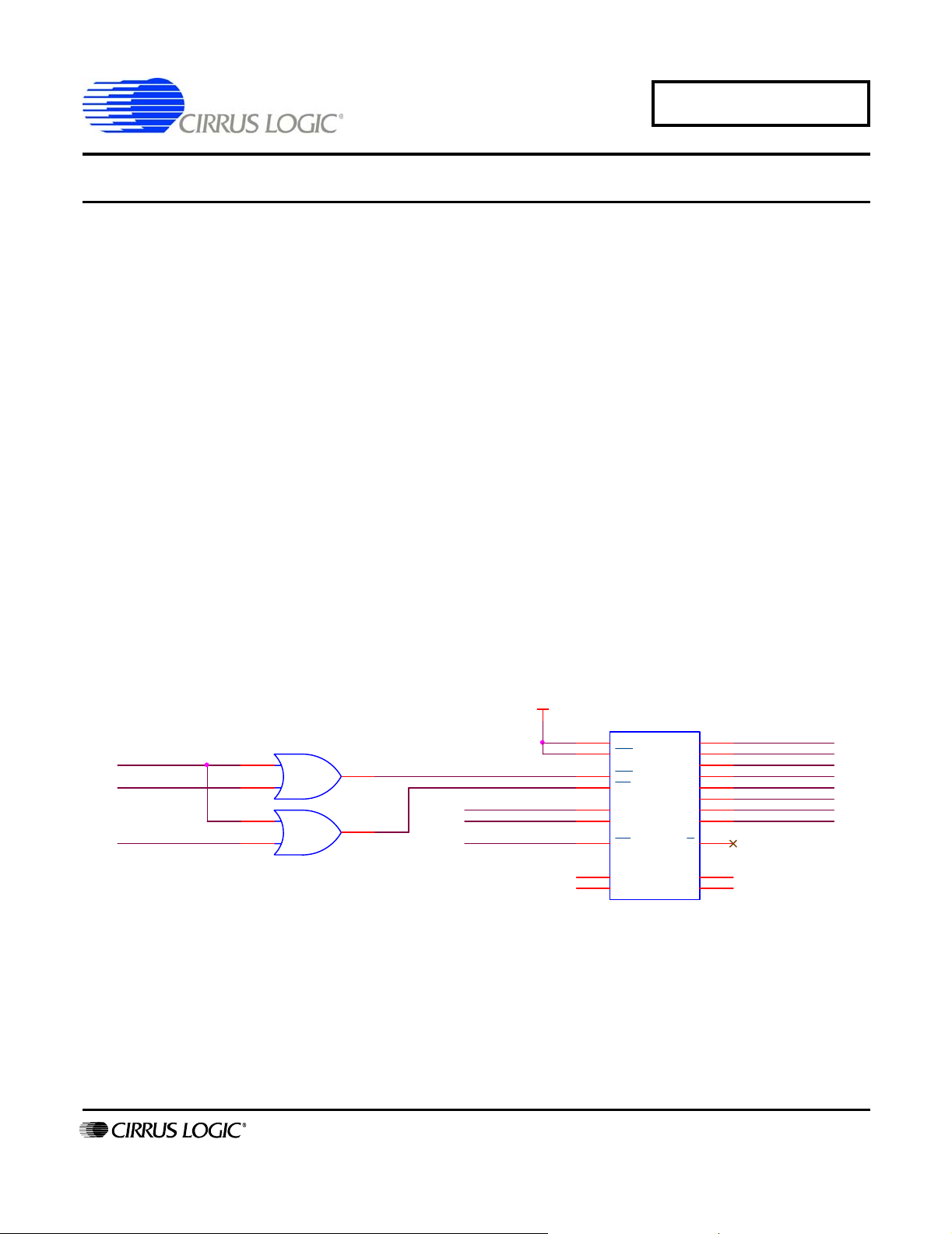
Please refer to the partial schematic below. GPIOx, GPIOy, and GPIOz may be any GPIO pins from the
EP93xx device. Not all of the devices in the EP93xx family have all of their GPIO port pins bonded out.
Refer to the datasheet for the specific device you are using. It is suggested that all the GPIO pins connected to the NAND device belong to the same port for efficient code. However, this is not a requirement.
There is no GPIO signal connected to pin 7 of the NAND device in the figure below. It is not required because the ready status can be read from a bit in the Status register. If the design uses pin 7, make sure
that the GPIO line used has interrupt capability. Referring to the EP93xx User's Guide, GPIO section, you
will notice Ports A, B, and F have interrupt capability. Note that Port A and B have interrupt capability but
it is implemented as a single interrupt signal called GPIOINTR. All pins on Port F are availab le to the system interrupt controller as GPIO[7:0]INTR.
The example below connects an EP93xx to the SAMSUNG K9F2G08U0M.
/CSx
/WE
/RE
http://www.cirrus.com
PWR_3V3
U2
38
1
2
1
2
3
3
/NAND_WE
/NAND_RE
GPIOz
GPIOy D0
GPIOx
19
18
8
17
16
9
12
37
K9F2G08
Figure 1. Example of Implementation Using Minimal GPIO
Copyright © Cirrus Logic, Inc. 2005
(All Rights Reserved)
PRE
WP
WE
RE
ALE
CLE
CE
PWR_3V3
PWR_3V3
D7
D6
D5
D4
D3
D2
D1
D0
R/B
GND
GND
44
43
42
41
32
31
30
29
7
13
36
D7
D6
D5
D4
D3
D2
D1
FEB ‘05
AN266REV1
1
Page 2
AN266
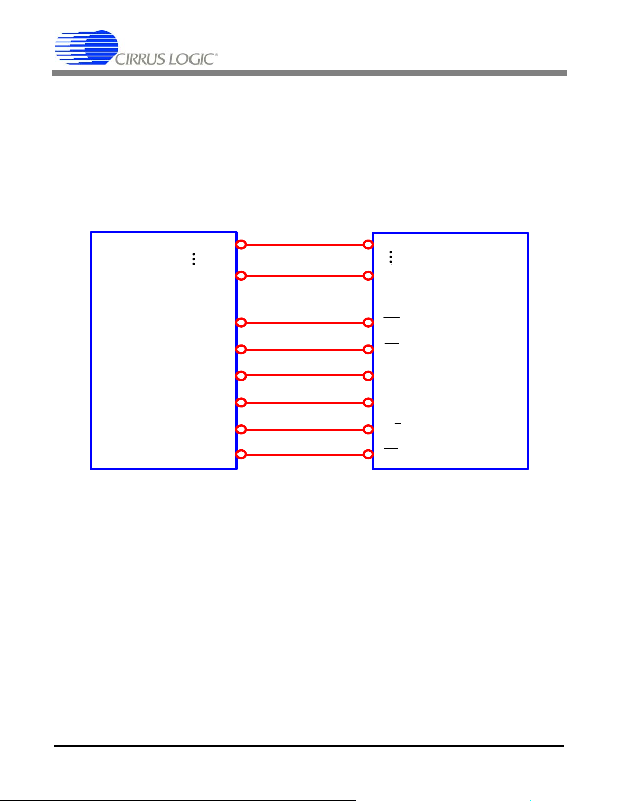
3. Implementation Using GPIO (for EP931x)
Alternatively, the general purpose I/O (GPIO) pins can be used to provide an easy way to control an external NAND flash memory device. EP93xx GPIO signals provide great flexibility in meeting the NAND
device timing requirements. However, this may not be the most efficient way to connect an EP931x to a
NAND flash memory device because it requires the use of many of the available GPIO pins.
The example below connects an EP931x to the SAMSUNG K9F2G08U0M. See “Read Flash ID” Sample
Code on page 3 for a code example for this particular approach.
EP931x
GPIO Port C[0]
GPIO Port C[7]
GPIO Port B[1]
GPIO Port B[2]
GPIO Port B[3]
GPIO Port B[4]
GPIO Port B[5]
GPIO Port B[6]
…
Figure 2. Example of Implementation Using GPIO Ports B and C
I/O0
…
I/O7
WE
RE
ALE
CLE
R/B
CE
K9F2G08U0M
2 AN266REV1
Page 3

3.1 “Read Flash ID” Sample Code
ULONG ulMakerCode;
ULONG ulDeviceCode;
ULONG ulIDData;
*GPIO_PBDDR = 0x5E;
//
// Write Read ID Command
//
*GPIO_PBDR = 0x14;
*GPIO_PCDR = 0x90;
*GPIO_PCDDR = 0xFF;
*GPIO_PBDR = 0x06;
//
// Write Reading ID Address
//
*GPIO_PBDR = 0x0C;
*GPIO_PCDR = 0x00;
*GPIO_PCDDR = 0xFF;
*GPIO_PBDR = 0x06;
//
// Prepare to Read Data from IO
//
*GPIO_PCDDR = 0x00;
AN266
//
// Read Maker Code
//
*GPIO_PBDR = 0x02;
ulMakerCode = *GPIO_PCDR;
*GPIO_PBDR = 0x06;
//
// Read Device Code
//
*GPIO_PBDR = 0x02;
ulDeviceCode = *GPIO_PCDR;
*GPIO_PBDR = 0x06;
//
// Don't care this byte
//
*GPIO_PBDR = 0x02;
ulIDData = *GPIO_PCDR;
*GPIO_PBDR = 0x06;
//
// Read Page Size, Block Size, Spare Size, Organization
//
*GPIO_PBDR = 0x02;
ulIDData = *GPIO_PCDR;
*GPIO_PBDR = 0x06;
// Disable NAND Flash
*GPIO_PBDR = DISABLE_CHIP;
printf("Maker Code = 0x%X\r\n",ulMakerCode);
printf("Device Code = 0x%X\r\n",ulDeviceCode);
printf("IDData = 0x%X\r\n",ulIDData);
AN266REV1 3
Page 4

AN266
Table 1. Revision History
Release Date Changes
REV1 Febuary 2005 Initial Release
Contacting Cirrus Logic Support
For a complete listing of Direct Sales, Distributor, and Sales Representative contacts, visit the Cirrus Logic web site at:
http://www.cirrus.com
IMPORTANT NOTICE
Cirrus Logic, Inc. and its subsidiaries ("Cirrus") believe that th e informatio n containe d in this docum ent is accur ate and reli able. Ho wever, the informa tion is subject
to change without notic e and is pr ovi ded "AS IS" with out warr ant y of an y kin d (ex press or im pli ed). Custo mers ar e adv ised to ob tain the latest version of relevant
information to verify, before placing orders, that information being relied on is current and complete. All products are sold subject to the terms and conditions of sale
supplied at the time of order acknowledgment, including those pertaining to warranty, indemnification, and limitation of liability. No responsibility is assumed by
Cirrus for the use of this information, including use of this inform ation as the basis for ma nufacture or sale of any items, or for infringement of patents or other rights
of third parties. This document is the property of Cirrus and by furnis hing this inform ation, Cirrus gran ts no license, express or implied under any patents, mask work
rights, copyrights, tr adema rks, tr ade secr ets or o the r i ntel lec tual pro pert y r ight s. Ci rrus owns the copy righ ts associ at ed wit h th e informat ion con tain ed herei n and
gives consent for copies to be made of the in formation on ly for use within your orga nization with respect to C irrus integrated circu its or other products o f Cirrus. This
consent does not extend to other copying such as co pyin g fo r general distribution, advertising or promotional purposes, or for creating any work for resale.
CERTAIN APPLICATIONS USING SEMICONDUCTOR PRODUCTS MAY INVOLVE POTENTIAL RISKS OF DEATH, PERSONAL INJURY, OR SEVERE PROPERTY OR ENVIRONMENTAL DAMAGE ("CRITICAL APPLICATIONS"). CIRRUS PRODUCTS ARE NOT DESI GNED, AUTHORIZED OR WARRANTED FOR
USE IN AIRCRAFT SYSTEMS, MILITARY APPLICATIONS, PRODUCTS SURGICALLY IMPLANTED INTO THE BODY, AUTOMOTIVE SAFETY OR SECURITY
DEVICES, LIFE SUPPORT PRODUCTS OR OTHER CRITICAL APPLICATIONS. INCLUSION OF CIRRUS PRODUCTS IN SUCH APPLICATIONS IS UNDERSTOOD TO BE FULLY AT THE CUSTOMER'S RISK AND CIRRUS DISCLAIMS AND MAKES NO WARRANTY, EXPRESS, STATUTORY OR IMPLIED, INCLUDING THE IMPLIED WARRANTIES OF MERCHANTABILITY AND FITNESS FOR PARTICULAR PU RPOSE, WITH REGARD TO ANY CIRRUS PRODUCT THAT
IS USED IN SUCH A MANNER. IF THE CUSTOMER OR CUSTOMER'S CUSTOMER USES OR PERMITS THE USE OF CIRRUS PRODUCTS IN CRITICAL
APPLICATIONS, CUSTOMER AGREES, BY SUCH USE, TO FULLY INDEMNIFY CIRRUS, ITS OFFICERS, DIRECTORS, EMPLOYEES, DISTRIBUTORS AND
OTHER AGENTS FROM ANY AND ALL LIABILITY, IN CLUDING ATT ORNEYS' F EES AND COSTS, T HAT MAY RESULT FROM OR ARISE IN CONNECTION
WITH THESE USES.
Cirrus Logic, Cir rus, Maver ic kCrun ch, Maveric kKey , and t he Cir rus Logi c logo desi gns ar e tr ademar ks of Cirr us Lo gic, Inc. All oth er br and an d prod uct n ames i n
this document may be trademarks or service marks of their respective owners.
Microsoft, Windows, Windows CE are registered trade m a rks of Microsoft Corp oratio n.
MicrowireTM is a trademark of National Semiconductor Corp. National Semiconductor is a registered trademark of National Semiconductor Corp.
Texas Instruments is a registered trademark of Texas Instruments, Inc.
Motorola is a reigistered trademark of Motorola, Inc.
LINUX is a registered trademark of Linus Torvalds.
RedBoot is a registered trademark of Red Hat, Inc.
4 AN266REV1
 Loading...