

Page 1
AN265
EP93xx RTC Oscillator Circuit
Note: This application note is applicable to all revisions of the EP93xx device.
1. BACKGROUND
Cirrus Logic has found that the Real Time Clock (RTC) circuit in the current EP93xx devices is susceptible
to on-chip noise, which can generate an inaccurate clock count and possibly cause the IC to boot into an
improper state during power-up.
To correct this issue, customers need to provide a clean square wave input to the RTCXTALI pin. This
may be accomplished several ways, such as by using an external clock oscillator or a dedicated RTC chip
like the DS1337. This application note, however, shows the use of an external Pierce oscillator circuit to
replace the existing internal RTC circuit.
Please note that an external RTC oscillator circuit is required for the EP93xx family on both existing and
future revision parts.
2. IMPLEMENTATION
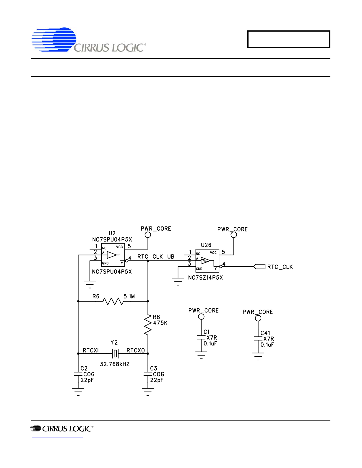
Figure 1. Implementation Using a Pierce Oscillator Circuit and Schmitt-trigger Inverter
http://www.cirrus.com
Copyright © Cirrus Logic, Inc. 2005
(All Rights Reserved)
DEC ‘05
AN265REV2
Page 2
AN265
The NC7SPU04 is an unbuffered inverter that is powered from the 1.8 VDC rail. The output of the
NC7SPU04 connects to the RTCXTALI input on the EP93xx device. The RTCXTALO pin is left open. The
exact value of the capacitors may need to be adjusted based on the actual crystal used and the layout
and routing of the circuit. Care should be taken to minimize the trace lengths and to avoid high-speed signals near the oscillator input. The 475 kΩ resistor (R2) ensures that the crystal is not overdriven. Overdriving the crystal can lead to premature aging and failure of the crystal. The RTC clock is vital to booting
up the EP93xx devices. Without an RTC clock, the EP93xx processor will not boot.
A Schmitt-trigger inverter has been added to the output of the oscillator circuit. The new inverter is also
powered off the 1.8 VCD rail, referred to as PWR_CORE in Figure 1. The Schmitt-trigger inverter has
been added so that the EP93xx device will only receive a full-scale RTC clock. The Schmitt-trigger inverter
will not produce a clock output until the RTC oscillator has produced levels that meet the minimum input
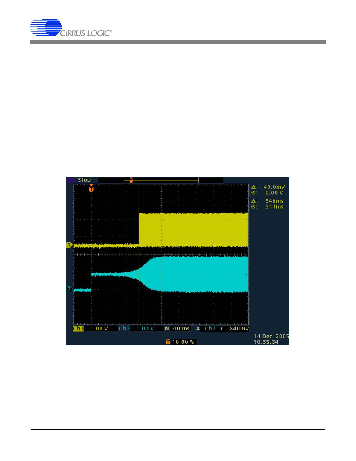
threshold level of the Schmitt-trigger inverter. Figure 2 shows the output from the new circuit, RTC_CLK
is on channel 1 and RTC_CLK_UB is on channel 2 in Figure 2.
Figure 2. Buffered and Unbuffered RTC Oscillator Output.
2 AN265REV2
Page 3

3. Determining the Silicon Revision of the Integrated Circuit
On the front of the integrated circuit, directly under the part number, is an alphanumeric line. Characters 5
and 6 in this line represent the silicon revision of the chip. For example, this line indicates that the chip is a
“E0” revision chip:
EFWAE0AM0340
Table 1: Revision History
Version Date Changes
REV1 NOV 2004 Initial release.
REV2 DEC 2005 Added Schmitt-trigger inverter.
AN265
Contacting Cirrus Logic Support
For all product questions and inquiries contact a Cirrus Logic Sales Representative.
To find the one nearest to you go to http://www.cirrus.com
IMPORTANT NOTICE
Cirrus Logic, Inc. and its subsidiaries ("Cirrus") believe that the information contained in this document is accurate and reliable. However, the information is subject
to change without notice and is provided "AS IS" without warranty of any kind (express or implied). Customers are advised to obtain the latest version of relevant
information to verify, before placing orders, that information being relied on is current and complete. All products are sold subject to the terms and conditions of sale
supplied at the time of order acknowledgment, including those pertaining to warranty, indemnification, and limitation of liability. No responsibility is assumed by
Cirrus for the use of this information, including use of this information as the basis for manufacture or sale of any items, or for infringement of patents or other rights
of third parties. This document is the property of Cirrus and by furnishing this information, Cirrus grants no license, express or implied under any patents, mask work
rights, copyrights, trademarks, trade secrets or other intellectual property rights. Cirrus owns the copyrights associated with the information contained herein and
gives consent for copies to be made of the information only for use within your organization with respect to Cirrus integrated circuits or other products of Cirrus. This
consent does not extend to other copying such as copying for general distribution, advertising or promotional purposes, or for creating any work for resale.
CERTAIN APPLICATIONS USING SEMICONDUCTOR PRODUCTS MAY INVOLVE POTENTIAL RISKS OF DEATH, PERSONAL INJURY, OR SEVERE PROPERTY OR ENVIRONMENTAL DAMAGE ("CRITICAL APPLICATIONS"). CIRRUS PRODUCTS ARE NOT DESIGNED, AUTHORIZED OR WARRANTED FOR
USE IN AIRCRAFT SYSTEMS, MILITARY APPLICATIONS, PRODUCTS SURGICALLY IMPLANTED INTO THE BODY, AUTOMOTIVE SAFETY OR SECURITY
DEVICES, LIFE SUPPORT PRODUCTS OR OTHER CRITICAL APPLICATIONS. INCLUSION OF CIRRUS PRODUCTS IN SUCH APPLICATIONS IS UNDERSTOOD TO BE FULLY AT THE CUSTOMER'S RISK AND CIRRUS DISCLAIMS AND MAKES NO WARRANTY, EXPRESS, STATUTORY OR IMPLIED, INCLUDING THE IMPLIED WARRANTIES OF MERCHANTABILITY AND FITNESS FOR PARTICULAR PURPOSE, WITH REGARD TO ANY CIRRUS PRODUCT THAT
IS USED IN SUCH A MANNER. IF THE CUSTOMER OR CUSTOMER'S CUSTOMER USES OR PERMITS THE USE OF CIRRUS PRODUCTS IN CRITICAL
APPLICATIONS, CUSTOMER AGREES, BY SUCH USE, TO FULLY INDEMNIFY CIRRUS, ITS OFFICERS, DIRECTORS, EMPLOYEES, DISTRIBUTORS AND
OTHER AGENTS FROM ANY AND ALL LIABILITY, INCLUDING ATTORNEYS' FEES AND COSTS, THAT MAY RESULT FROM OR ARISE IN CONNECTION
WITH THESE USES.
Cirrus Logic, Cirrus, and the Cirrus Logic logo designs are trademarks of Cirrus Logic, Inc. All other brand and product names in this document may be trademarks
or service marks of their respective owners.
AN265REV2 3
 Loading...