

Page 1
AN263
Audio Conversion Systems Noise Calculations and
Requirements
Steve Green
Technical Marketing Manager
Mixed-Signal Products
1. Introduction
The skills required to predict the dynamic range of a combined Analog-to-Digital converter (ADC) and Digital-to-Analog converter (DAC) system, as well as determine the noise requirements for the analog input
and output stages, should be considered essential for an audio systems designer. The techniques required are relatively basic in that they are generally covered in the first analog circuit analysis class in
most engineering programs. However, applying these techniques to the conversion processes often generates some level of confusion. This discussion will detail the steps required to apply these techniques
and determine this critical system performance parameter.
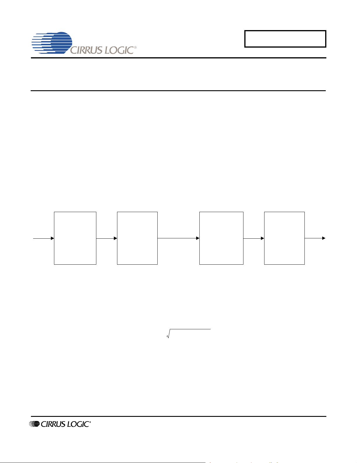
Buffer DACADC Filter
Figure 1. Conversion System Block Diagram
The ADC and DAC system, Figure 1, contains four primary noise sources that must be considered. These
include the analog input buffer, ADC, DAC and the analog output buffer/ filter stage. Noise generated in
each of these stages adds as the “square root of the sum of the squares” as shown below. This fundamental relationship will be used throughout this discussion.
2
2
2
V
total
V
V
+++=
1
2
2
V
V
3
4
The analysis requires several initial assumptions and setting of limits.
1) The bandwidth is set to 20 kHz. This constraint is purely for convenience and allows th e use of a common converter data sheet specification. The results can easily be scaled to other bandwidths as long
as assumption #2 remains valid.
2) The spectral content of the noise is “white”. This assumes that the contribution of 1/f noise is negligible
and the noise sources within the converters remain “white” to the upper limit of the analysis. A word
http://www.cirrus.com
Copyright © Cirrus Logic, Inc. 2004
(All Rights Reserved)
Oct ‘04
AN263REV1
Page 2

AN263
of warning, the spectral noise content of digital-to-analog converters often do not retain this characteristic at bandwidths well beyond 20 kHz when operated at 96 kHz or 192 kHz sample rates.
3) The noise contribution of the analog input and out put stages are negligible. This assumption simplifies
the initial analysis but requires further investigation to ensure accuracy.
2. Combined ADC and DAC Dynamic Range Calculation
2.1 Converter Equivalent Noise Calculation
Dynamic Range (DR) is a specification that can be found in any ADC or DAC data sheet. This specification
is defined as the ratio of the RMS voltage of a full-scale analog input ( V
) or output (V
fsadc
to the RMS noise voltage of the converter over a 20 kHz bandwidth. DR is generally specified in dB and
the equation for dynamic range is shown below. Notice that there are three variables in this equation,
where the DR and V
allow the calculation of the equivalent RMS noise voltage (V
are common data sheet specifications. The equation can be easily rearranged to
fs
) of the converter.
n
) sine wave
fsdac
V
fs
⎛⎞
------- -
DR 20
log×=
⎝⎠
V
n
V
------------------=
10
fs
DR
⎛⎞
-------- -
⎝⎠
20
V
n
However, adjustments to the data sheet Dynamic Range and full-scale input/output specifications are often required prior to the calculation.
1) Dynamic Range specifications are often A-weighted and the equivalent noise calculation requires the
use of un-weighted numbers. Fortunately, A-weighted specifications can easily be converted to an a pproximate unweighted specification. A conservative estimate can be determined by simply degrading
the A-weighted data sheet specification by 3 dB.
2) The full scale input or output voltage specifications in converter data sheets are commonly represented as either volts peak-to-peak, volts peak or RMS. The full scale input or output voltage must be converted to a RMS value for this calculation to be valid.
2.2 Conversion System Gain
Another requirement is that the noise sources within the system must be referenced to the same system
node. Assume that the ADC and DAC system operates as a single block with analog input and analog
output. Due to the differences in the conversion processes and the corresponding differences in the analog input voltage and the analog output voltage, the block has either gain or attenua tion. The system must
be modeled to reflect this gain with the gain coefficient (K), as shown in Figure 2.
2 AN263REV1
Page 3
AN263
V
fsadc
ADC
Figure 2. Effective Conversion System Gain
K
2.3 Equivalent System Noise Calculation
The output referred system noise voltage (V
) can be calculated using the expressions for the gain co-
nsys
efficient, equivalent ADC and DAC noise voltages.
V
nsys
V
ndac
Where:
V
ndac
K
V
fsdac
----------------=
V
fsadc
2
KV
×()
+()=
V
fsdac
------------------------=
DR
dac
⎛⎞
----------------
⎝⎠
20
10
nadc
DAC
2
V
fsdac
V
fsadc
V
nadc
------------------------=
DR
adc
⎛⎞
----------------
⎝⎠
20
10
V
fsdac
K
----------------=
V
fsadc
Following substitution and simplification:
DR
dac
⎛⎞
----------------
–
⎝⎠
10
V
nsysVfsdac
10
AN263REV1 3
10
+=
DR
adc
⎛⎞
----------------
–
⎝⎠
10
Page 4

AN263
2.4 System Dynamic Range Calculation
The un-weighted system dynamic range (in dB) can be calculated using the equation for the equivalent
system noise voltage. Conversion to A-weighting requires the addition of 3 dB to the un-weighted number.
V
fsdac
unweighted DR
Substituting and simplifying the equation yields;
sys
20
log×=
----------------
V
nsys
unweighted DR
A-weighted DR
10– 10
sys
= unweighted DR
sys
DR
dac
⎛⎞
----------------
–
⎝⎠
10
sys
DR
⎛⎞
----------------
–
⎝⎠
10
+log×=
+ 3 dB
adc
10
3. Converter and Buffer Noise Analysis
One of the initial assumptions was that the buffer noise was negligible in relation to the converter noise.
Of the assumptions during the initial analysis, this has the greatest potential of being in valid. Though this
assumption proves to be acceptable for many applications and converter products, it becomes questionable as converter dynamic range improves.
The calculation of the equivalent noise voltages for the ADC input buffers and DAC output buffers / filters
is beyond the scope of this paper. However, care needs to be taken to ensure that the converter and buffer
noise sources are referred to the appropriate system node. The converters themselves can be considered
unity gain devices and their noise can be referred to either the input or output of the converter. It’s generally best to refer the ADC buffer noise to the input of the ADC. In the case of the DAC, it is most convenient
to refer the noise of the DAC and buffer to the output of the buffer.
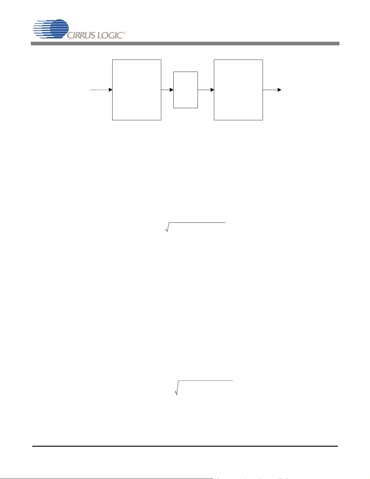
To illustrate the technique let's take a look at the combination of an input buffer and ADC, Figure 3. The
combined converter + buffer noise equation is shown below, assuming the buffer noise is referred to the
input of the ADC. The equivalent converter noise voltage can be calculated as previously shown.
Buffer ADC
Figure 3. Input Buffer and ADC Block Diagram
V
nT
V
2
nadc
+=
2
V
nbuffer
4 AN263REV1
Page 5

AN263
3.1 Generalized Noise Error
It is very informative to create a generalized noise relationship and a “rule-of-thumb” design g oal such that
the noise contribution of the buffer can be considered negligible. Taking the total noise equation, and dividing each of the contributing noise sources by the converter noise as shown below can easily accomplish this. Converting the normalized noise to dB, creates a very informative relationship in that the
deviation from 0 dB can now interpreted as the normalized error function.
V
nT
normalized
V
nconverter
⎛⎞
-----------------------------
⎝⎠
V
nconverter
2
V
nbuffer
⎛⎞
---------------------------- -
+=
⎝⎠
V
nconverter
V
nbuffer
⎛⎞
V
nT
normalized
---------------------------- -
1
+=
⎝⎠
V
nconverter
2
2
Error 20 1
V
nbuffer
⎛⎞
-----------------------------
+log×=
⎝⎠
V
nconverter
2
Figure 4 shows the normalized noise error as a function of ratio of buffer to converter noise. The X-axis
shows the ratio and the Y-axis displays the deviation from 0 dB. Notice that as the ratio approaches 1,
where the buffer noise is equivalent to the converter noise, the error is 3 dB. The graph also indicates that
an error of approximately 1 dB is introduced when the noise of the buffer noise is 1/2 that of the converter.
Figure 5 shows the previous normalized noise error with a change in the scaling of the X-axis and Y-axis.
Notice that at the point where buffer noise is 10% that of the converter noise, the error is approximately
0.05 dB. This error can probably be considered negligible for even the most demanding of applications. It
is also convenient that a ratio of 0.1 is equiva lent to a buffer noise voltage that is 20 dB below the converter
noise voltage. This indicates that a conservative and convenient “rule-of-thumb” desig n goal is for the buffer noise to be 20 dB below that of the converter. However, the ultimate decision on the minimum required
buffer noise is based on systems performance and cost requirements and may differ from this “rule-ofthumb”.
AN263REV1 5
Page 6

AN263
Normalized Noise Error
3
2.5
2
1.5
1
Error introduced by Buffer Noise
0.5
0
0 0.1 0.2 0.3 0.4 0.5 0.6 0.7 0.8 0.9 1
Ratio of Buffer noise to Converter noise
Figure 4. Normalized Noise Error - Wide View
1
0.9
0.8
0.7
0.6
0.5
0.4
Error introduced by Buffer Noise
0.3
0.2
0.1
0
0 0.05 0.1 0.15 0.2 0.25 0.3 0.35 0.4 0.45 0.5
Ratio of Buffer noise to Converter noise
Figure 5. Normalized Noise Error - Zoomed View
6 AN263REV1
Page 7

AN263
3.1.1 Illustrative Noise Budget Calcu l at io n
Let's calculate the required buffer noise for the CS5381 to meet the assumption of negligible noise contribution using the “rule-of-thumb” design goal. The equivalent noise of the CS5381 can be calculated as
previously shown using the relevant data sheet specifications, where the un-weighted Dynamic Range is
117 dB and the full-scale differential input is 2 Vrms. This calculation shows that the equivalent noise for
the CS5381 is 2.83 µV. Based on the “rule-of-thumb” noise requirement, the buffer noise sh ould be 20 dB
below the equivalent converter noise, or 0.283 µV.
It is informative and enlightning to compare this noise voltage to the equivalent noise generated by a resistor at room temperature (25 degrees C). The following is the equation used to calculate the noise for
a resistor.
V
n
resistor
4kTBR=
Where:
- k = 1.38 x 10⁻²³ Joules / degree (Boltzman's Constant)
- T = Absolute temperature of the resistor
- B = effective bandwidth (20 kHz for this example)
- R = resistance value
Solving this equation for the resistance and inserting the buffer noise voltage design goal indicates that
the noise contribution of the buffer must be equal to or less than the equivalent noise of a 243 ohm resistor! It's apparent that in the case of high-dynamic range converters, the n oise contribution of the input and
output buffers cannot be assumed to be negligible. Low noise design techniques for the analog buffers
must be employed to achieve the full performance capabilities of leading edge converters.
3.2 Combined Converter and Buffer Dynamic Range from a different perspective
It is interesting to look at this relationship from the perspective of the deviation from ideal as the converter
dynamic range increases and the buffer noise remains constant. This has been a relatively common occurrence over the past few years as systems designers have been assigned the goal of updating an existing product by increasing the system dynamic range. The obvious solution is to replace the existing
converters with higher dynamic range converters. Unfortunately, the assumption is often made that the
noise contribution of the existing buffer design is negligible, which often leads to disappointing results and
subsequent redesign.
Figure 6 displays the results of this situation with a hypothetical D/A and filter design. The X-axis of the
graph indicates the converter dynamic range and the Y-axis indicates the dynamic range of the combined
filter / buffer and D/A converter. The upper plot indicates the ideal dynamic range where the buffer noise
is zero. The remaining plots indicate the degradation in performance with a fixed buffer noise contribution
for four different converter full-scale output voltages. Notice that, for this example, the deviation from ideal
for the converters with dynamic ranges in the 100 to 1 05 dB range is minimal. However, as converter performance exceeds 105 dB the deviation becomes significant.
AN263REV1 7
Page 8

AN263
yyg
120
118
116
114
112
110
108
System Dynamic Range (dB)
106
104
102
100
100 105 110 115 120 125 130
DAC Dynamic Range (dB)
Ideal DR
10k Filter + 3.536Vrms
10k Filter + 2.475Vrms
10k Filter + 1.945Vrms
10k Filter + 1.768Vrms
Figure 6. System vs. DAC Dynamic Range - 10K Filter
120
118
116
114
112
110
108
System Dynamic Range (dB)
106
104
102
100
100 105 110 115 120 125 130
DAC Dynamic Range (dB)
Ideal DR
1k Filter + 3.536Vrms
1k Filter + 2.475Vrms
1k Filter + 1.945Vrms
1k Filter + 1.768Vrms
Figure 7. System vs. DAC Dynamic Range - 1K Filter
8 AN263REV1
Page 9

AN263
Figure 7 displays a similar series of plots where the filter/ buffer circuit has been redesigned to scale the
resistors to 10% of the previous values. Notice the improvements in the deviation from the ideal. With
these impedance changes, the deviation from the ideal remains minimal up to approximately 110 dB.
4. Conclusion
It is a relatively straightforward process to calculate and predict the system dynamic range for any combination of analog-to-digital and digital-to-analog converter, as well as the maximum allowable analog
buffer and filter noise to achieve these targets. The difficulty is designing low noise analog buffers and
filters that meet the requirements of today’s leading edge converters. The combination of high-dynamic
range and the limited full-scale signal amplitudes typical of today’s converters create a challenging enviroment for the systems designer. The first steps are to recognize and understand the challenge.
AN263REV1 9
Page 10

Revision Date Changes
1 18 Oct 2004 Initial Release
AN263
Contacting Cirrus Logic Support
For all product questions and inquiries contact a Cirrus Logic Sales Representative.
To find one nearest you go to //www.cirrus.com
IMPORTANT NOTICE
Cirrus Logic, Inc. and it s su bsi di a ri es ( “Ci rr u s”) be li ev e th at t h e information contained in th i s docu ment is acc ur at e and re liable. However, the information is subject
to change without not ice and is pr ovided “AS IS” withou t warrant y of any kind ( express or implied) . Custome rs are advi sed to obt ain the lat est version of relevant
information to verify, before placing orders, that information being relied on is current and complete. All products are sold subject to the terms and conditions of sale
supplied at the time of order acknowledgment, including those pertaining to warranty, patent infringement, and limitation of liability. No responsibility is assumed by
Cirrus for the use of this information, including use of this information as the basis for manufacture or sale of any items, or for infringement of patents or other rights
of third parties. This document is the property of Cirrus and by furnishing this information, Cirrus grants no license, express or implied under any patents, mask work
rights, copyright s, trademarks, trade secret s or other intellectua l property r ights. Cirr us owns the copy rights associ ated with the informat ion containe d herein and
gives consent for copies to be made of the information only for use within your organization with respect to Cirrus integrated circuits or other products of Cirrus. This
consent does not extend to other copying such as copying for general distribution, advertising or promotional purposes, or for creating any work for resale.
CERTAIN APPLICATIONS USING SEMI CONDUCT OR PRO DUCTS MAY I NVOL VE POT ENT IA L RI SKS OF DEA T H, PE RS ONAL I NJ URY , OR SEVE RE P ROPERTY OR ENVIRONMENTAL DAMAGE (“CRITICAL APPLICATIONS”). CIRRUS PRODUCTS ARE NOT DESIGNED, AUTHORIZED OR WARRANTED FOR USE
IN AIRCRAFT SYSTEMS, MILITARY APPLICATIONS, PRODUCTS SURGICALLY IMPLANTED INTO THE BODY, LIFE SUPPORT PRODUCTS OR OTHER CRITICAL APPLICATIONS (INCLUDING MEDICAL DEVICES, AIRCRAFT SYSTEMS OR COMPONENTS AND PERSONAL OR AUTOMOTIVE SAFETY OR SECURITY DEVICES). INCLUSION OF CIRRUS PRODUCTS IN SUCH APPLICATIONS IS UNDERSTOOD TO BE FULLY AT THE CUSTOMER'S RISK AND CIRRUS
DISCLAIMS AND MAKES NO WARRANTY, EXPRESS, STATUTORY OR IMPLIED, INCLUDING THE IMPLIED WARRANTIES OF MERCHANTABILITY AND FITNESS FOR PARTICULAR PURPOSE, WITH REGARD TO ANY CIRRUS PRODU CT THAT IS USED IN SUCH A MANNER. IF THE CUSTOMER OR CUSTOMER'S
CUSTOMER USES OR PERMITS THE USE OF CIRRUS PRODUCTS IN CRITICAL APPLICATIONS, CUSTOMER AGREES, BY SUCH USE, TO FULLY INDEMNIFY CIRRUS, ITS OFFICERS, DIRECTORS, EMPLOYEES, DISTRIBUTORS AND OTHER AGENTS FROM ANY AND ALL LIABILITY, INCLUDING ATTORNEYS'
FEES AND COSTS, THAT MAY RESULT FROM OR ARISE IN CONNECTION WITH THESE USES.
Cirrus Logic, Cirrus, and the Cirrus Logic logo designs are trademark s of Cirrus Logic, Inc. All other brand and product names in this document may be trademarks
or service marks of their respective owners.
10 AN263REV1
 Loading...