

Page 1
AN259
Transitioning from the CS4382 to the CS4382A or CS4385
1. Introduction
This application note describes how to transition easily to the CS4385 or CS4382A from an existing
design which uses the CS4382. The CS4382A was designed to give a simple upgrade path from the
CS4382 whereas the CS4385 adds some additional features. Please refer to the CS4382A and CS43 85
data sheets for supplemental information and specifications concerning operation of the device. A brief
comparison between the product families is shown in Table 1.
1.1 What the CS4382A offers over the CS4382:
• Sixth order multi-bit delta-sigma modulator for lower out of band noise
• Increased full-scale output level for ease of board level noise management
• Improved lower latency PCM digital filter
• Non-decimating DSD processor with on chip 50 kHz filtering
• Uses identical register mapping
1.2 Changes from the CS4382 that the CS4382A requires:
• The VD supply must be changed to 2.5 V from either the 3.3 V or 5 V of the CS4382
•
Depending on the desired output voltage require ments, attenuation may need to be added to the off-chip filter.
• Loss of simultaneous support for two synchronous sample rates mode which was available in the CS43 82.
This mode provided for dual sample rates such as
DVD audio and required the use of
LRCK2 and SCLK2. This mode is not offered in the CS4382A or
CS4385.
• Additional resistors on MUTEC pins
192 kHz front channels with 96 kHz surrounds for
1.3 What the CS4385 offers over the CS4382A:
• Additional DSD functions of Volume control, Mute pattern detect, support for phase modulation mode, and
offers a direct to switched capacitor path.
• 1/2 dB volume control steps (vs. 1 dB in CS4382/82A)
• One-Line and TDM modes
• Auto-mute polarity detection
• Auto-speed mode detection
1.4 Changes from the CS4382 that the CS4385 requires:
• The VD supply must be changed to 2.5 V from the either 3.3 V or 5 V of the CS4382
•
Depending on the desired output voltage requirements, attenuation may need to be added to the off-chip filter.
• Simultaneous support for two synchronous sample rates is no longer available
• Additional resistors on MUTEC pins
• 4 pins change location or function for hardware mode. The changes aren't necessary for software mode.
• Requires different register mapping from the CS4382
http://www.cirrus.com
Copyright © Cirrus Logic, Inc. 2009
(All Rights Reserved)
AN259REV2
JAN ‘09
1
Page 2

AN259
CS4385 CS4382A CS4382
Dynamic Range
THD+N
Resolution
Sample Rate
Pow er Suppl y
Volume Control 0.5 dB
Auto F s De tect Yes
Package 48-LQFP
Table 1. Product Comparison
dB
dB
bits
kHz
VA
VD
114
-100
24
192
5
2.5
For users of the CS4382, the CS4385 is a simple, yet affordable, upgrade to a richer feature set and lower
out-of-band noise performance.
2. The Design Transition
2.1 Transitioning from the CS4382 to CS4382A
2.1.1 Hardware changes
114 114
-100 -100
24 24
192 192
55
2.5 3.3 to 5
1 dB 1 dB
No No
48-LQFP 48-LQFP
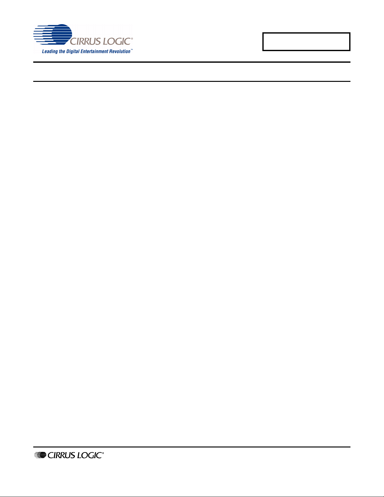
The CS4382A pinout was primarily based on the CS4382 with only 2 pins changing function. Other
pins have new recommended components but the circuit topologies remain the same and thu s do n ot
require modification to the PCB. The most significant change is that the VD core of the CS4382A
requires 2.5 V for operation, whereas the CS4382 was able to run from 3.3 V to 5 V. The CS4382A will
NOT operate off of a VD supply of 3.3 V or 5 V.
Figure 1 and Figure 2 show the CS4382 and CS4382A pinouts respectively. The changes to the two
pinouts are highlighted. Figure 1 highlights the pins which have changed function and which may
require a PCB change. Figure 2 highlights the pins which have new recommended components.
2 AN259REV2
Page 3
AN259
AOUTA1-
AOUTA1+
VQ
MUTEC234
AOUTB1+
AOUTB4-
AOUTB1-
36
AOUTA2-
35
AOUTA2+
AOUTB2+
34
33
AOUTB2-
32
VA
31
GND
AOUTA3-
30
AOUTA3+
29
AOUTB3+
28
27
AOUTB3-
AOUTA4-
26
AOUTA4+
25
AOUTB4+
DSDA2
DSDB1
DSDA1
VD
GND
MCLK
LRCK1(DSD_EN)
SDIN1
SCLK1
LRCK2
SDIN2
SCLK2
MUTEC1
AOUTA1-
VLS
M3(DSD_SCLK)
DSDB4
DSDB3
DSDA4
DSDB2
DSDA3
48 47 46 45 44 43 42 41 40 39 38 37
1
2
3
4
5
6
7
8
9
10
11
12
13 14 15 16 17 18 19 20 21 22 23 24
SDIN3
= denotes location or function changes
when trasitioning to CS4382A
SDIN4
CS4382
M1(SDA/CDIN)
M2(SCL/CCLK)
VQ
RST
VLC
FILT+
M0(AD0/CS)
Figure 1. CS4382 pinout
AOUTA1+
MUTEC234
AOUTB1-
AOUTB1+
36
AOUTA2-
35
AOUTA2+
AOUTB2+
34
33
AOUTB2-
32
VA
31
GND
AOUTA3-
30
AOUTA3+
29
AOUTB3+
28
27
AOUTB3-
AOUTA4-
26
AOUTA4+
25
AOUTB4-
AOUTB4+
DSDA2
DSDB1
DSDA1
VD
GND
MCLK
LRCK1(DSD_EN)
SDIN1
SCLK1
TST
SDIN2
TST
1
2
3
4
5
6
7
8
9
10
11
12
= denotes pins which require changes
DSDB3
DSDA4
DSDB2
DSDA3
48 47 46 45 44 43 42 41 40 39 38 37
CS4382A
13 14 15 16 17 18 19 20 21 22 23 24
SDIN4
SDIN3
M1(SDA/CDIN)
M2(SCL/CCLK)
to components or voltages
VLS
DSDB4
VLC
M0(AD0/CS)
MUTEC1
M3(DSD_SCLK)
RST
FILT+
Figure 2. CS4382A pinout
Location or function changes as denoted in Figure 1 are as follows:
• The CS4385 does not support the simultaneous synchronous sample rate function of the CS4382. Pins 10
and 12 are now Test inputs.
Pins which require changes to external components or voltages as denoted in Figure 2 are as follows:
• Pin 4 (VD) requires 2.5 V for recommended operation. The CS4382 used either 3.3 V or 5 V, which, if left
unchanged, would damage the CS4382A.
• Pin 22 (MUTEC234) and pin 41 (MUTEC1) require an additional pull-up or down in order to mute during
reset. While reset is asserted these pins are high impedance and will not drive the mute circuitry. It is
recommended that the pull-up/down resistance properly biases the off-chip mute circuit into muting.
• Pins 23 - 30, 33 - 40 (AOUTs) have a new recommended filter circuit. This filter uses the same filter topology
as the CS4382. The component values have been changed to account for the extra output level from the
CS4382A and still provide 2 Vrms on the output. A general optimization was also made in order to reduce
the thermal noise contribution of the resistances (using smaller resistances where possible). Please refer to
the CS4382A datasheet for details on the new recommended filter.
2.1.2 Functional changes
- With the addition of the non-decimating DSD processor mode comes the added benefits of
matched PCM and DSD output levels and an on chip 50 kHz filter.
- The CS4382A uses a new multi-bit Delta-Sigma modulator core with mis-match shaping which al-
lows for lower over-all out-of-band noise and improved audio quality.
- The CS4382A gained new digital filters with improved stop-band performance and lower latency.
- The full scale differential output voltage has increased which needs to be accounted for in the an-
AN259REV2 3
Page 4
AN259
alog filter gain (if similar output level to the CS4382 is desired).
- The mute control pins are high impedance while reset is asserted. An external pull-up or down is
required to properly bias the off-chip mute circuit into muting during reset.
- The dual serial port function of the CS4382 which accepted two simultaneous synchronous sample rates (such as 192 kHz front and 96 kHz surrounds) is not supported.
2.2 Transitioning from the CS4382 to CS4385
2.2.1 Hardware changes
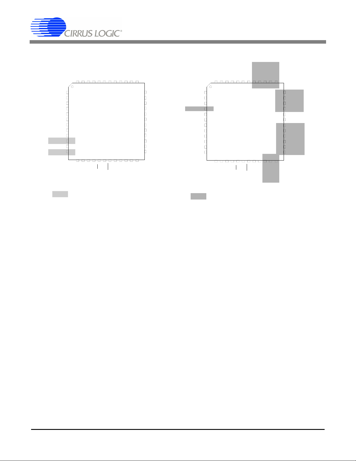
The CS4385 pinout was primarily based on the CS4382 with only 3 pins changing function. Other pins
have new recommended components but the circuit topologies remain the same and thus do not
require modification to the PCB. The most significant change is that the VD core of the CS4385
requires 2.5 V for operation, whereas the CS4382 was able to run from 3.3 V to 5 V. The CS4385 will
NOT operate off of a VD supply of 3.3 V or 5 V.
Figure 3 and Figure 4 show the CS4382 and CS4385 pinouts respectively. The changes to the two
pinouts are highlighted. Figure 3 highlights the pins which have changed function and which may
require a PCB change. Figure 4 highlights the pins which have new recommended components.
AOUTB1+
AOUTA1+
MUTEC234
AOUTB1-
36
35
34
33
32
31
30
29
28
27
26
25
AOUTB4-
AOUTB4+
AOUTA2AOUTA2+
AOUTB2+
AOUTB2VA
GND
AOUTA3AOUTA3+
AOUTB3+
AOUTB3AOUTA4-
AOUTA4+
DSDA2
DSDB1
DSDA1
VD
GND
MCLK
LRCK1(DSD_EN)
SDIN1
SCLK1
LRCK2
SDIN2
SCLK2
MUTEC1
AOUTA1-
VLS
M3(DSD_SCLK)
DSDB4
DSDA4
DSDB3
DSDB2
DSDA3
48 47 46 45 44 4 3 42 41 40 39 38 37
1
2
3
4
5
6
7
8
9
10
11
12
13 14 15 16 17 1 8 19 20 21 22 23 24
SDIN3
= denotes location or function changes
when trasitioning to CS4385
SDIN4
CS4382
M1(SDA/CDIN)
M2(SCL/CCLK)
VQ
RST
VLC
FILT+
M0(AD0/CS)
Figure 3. CS4382 pinout
AOUTA1+
MUTEC234
AOUTA1-
VLS
DSDB3
DSDA3
AOUTB1-
AOUTB1+
36
AOUTA2AOUTA2+
35
AOUTB2+
34
AOUTB2-
33
32
VA
31
GND
AOUTA3-
30
AOUTA3+
29
AOUTB3+
28
27
AOUTB3-
AOUTA4-
26
AOUTA4+
25
AOUTB4-
AOUTB4+
DSDA2
DSDB1
DSDA1
VD
GND
MCLK
LRCK
SDIN1
SCLK
M4
SDIN2
M3
DSDB2
48 47 46 45 44 43 42 41 40 39 38 37
1
2
3
4
5
6
7
8
9
10
11
2
1
13 14 15 16 17 18 19 20 21 22 23 24
SDIN3
DSDA4
CS4385
SDIN4
M1(SDA/CDIN)
M2(SCL/CCLK)
= denotes pins which require changes
to components or voltages
MUTEC1
DSDB4
DSD_SCLK
VQ
VLC
RST
FILT+
M0(AD0/CS)
Figure 4. CS4385 pinout
Location or function changes as denoted in Figure 3 are as follows:
• Pin 7 is no longer DSD_EN in hardware mode. In order to enter DSD mode on the CS438 5 you mu st either
set the M4 and M3 pins accordingly or use SPI™ or I
• The CS4385 does not support the simultaneous synchronous sample rate function of the CS4382. Pins 10
and 12 are now dedicated for stand-alone configuration (voltage input on these pins are still referenced to
VLS).
• Pin 42 no longer functions as M3 in stand-alone PCM modes. It is now a dedicated DSD_SCLK pin.
4 AN259REV2
2
C configuration.
Page 5

AN259
Pins which require changes to external components or voltages as denoted in Figure 4 are as follows:
• Pin 4 (VD) requires 2.5 V for recommended operation. The CS4382 used either 3.3 V or 5 V, which, if left
unchanged, would damage the CS4385.
• Pin 22 (MUTEC234) and pin 41 (MUTEC1) require an additional pull-up or down in order to indicate the
desired direction of mute polarity. While reset is asserted these pins are high impedance and will not drive
the mute circuitry. It is recommended that the pull-up/down resistance properly biases the off-chip mute
circuit into muting.
• Pins 23 - 30, 33 - 40 (AOUTs) have a new recommended filter circuit. This filter uses the same filter topology
as the CS4382. The component values have been changed to account for the extra output level from the
CS4385 and still provide 2 Vrms on the output. A general optimization was also made in order to reduce the
thermal noise contribution of the resistances (using smaller resistances where possible). Please refer to the
CS4385 datasheet for details on the new recommended filter.
2.2.2 Functional changes
- The CS4385 uses a new register mapping in order to accommodate the additio nal features which
it provides over the CS4382. Please refer to the CS4385 datasheet for the new mapping.
- With the addition of the non-decimating DSD processor mode comes the added benefits of
matched PCM and DSD output levels, DSD volume control, an on chip 50 kHz filter, Phase Modulation input mode, and DSD mute pattern detection. A direct DSD path to the switched capacitor
array is also offered. All of the features are accessed through the configuration registers.
- The CS4385 supports a setting for auto-selection of the speed mode to set what sample rate range
the DAC is to expect. This allows the CS4385 to operate at sample rates from 4 kHz on up to
192 kHz without intervention (Note: there are a few reserved frequencies, see datasheet for details). This setting is available in both stand-alone and control-port operation.
- The volume control in the CS4385 offers 0.5 dB step sizes for more volume setting resolution.
- The CS4385 offers TDM and One-Line modes for compatibility with various multi-channel surround sound DSPs which helps reduce board real-estate from the additional data lines. These
modes are not available in stand-alone mode.
- The CS4385 uses a new multi-bit Delta-Sigma modulator core with mis-match shaping which allows for lower over-all out-of-band noise and improved audio quality.
- The CS4385 gained new digital filters with improved stop-band performance and lower latency.
- The full scale differential output voltage has increased which needs to be accounted for in the analog filter gain (if similar output level to the CS4382 is desired).
- The mute control pins now support auto polarity detection. This allows for selection of active high
or low mute circuitry without the need to set registers. An external pull-up or down is required to
set the mute polarity.
- The MCLK divide by 2 bit is no longer necessary to access the 1024x MCLK/LRCK ratio (SSM),
512x MCLK/LRCK ratio (DSM) and 256x MCLK/LRCK ratio. A new ratio of 1152x has been added
for 32 kHz operation.
- The dual serial port function of the CS4382 which accepted two simultaneous synchronous sample rates (such as 192 kHz front and 96 kHz surrounds) is not supported.
AN259REV2 5
Page 6

AN259
Table 2. Revision History
Release Date Changes
REV1 JAN 2005 Initial Release
REV2 JAN 2009 Added text to indicate MUTEC pins of the CS4382A are high impedance
during reset
Contacting Cirrus Logic Support
For a complete listing of Direct Sales, Distributor, and Sales Representative contacts, visit the Cirrus Logic web site at:
http://www.cirrus.com
IMPORTANT NOTICE
Cirrus Logic, Inc. and its subsidiaries ("Cirrus") believe that th e informatio n containe d in this docum ent is accur ate and reli able. Ho wever, the informa tion is subject
to change without notic e and is pr ovi ded "AS IS" with out warr ant y of an y kin d (ex press or im pli ed). Custo mers ar e adv ised to ob tain the latest version of relevant
information to verify, before placing orders, that information being relied on is current and complete. All products are sold subject to the terms and conditions of sale
supplied at the time of order acknowledgment, including those pertaining to warranty, indemnification, and limitation of liability. No responsibility is assumed by
Cirrus for the use of this information, including use of this inform ation as the basis for ma nufacture or sale of any items, or for infringement of patents or other rights
of third parties. This document is the property of Cirrus and by furnis hing this inform ation, Cirrus gran ts no license, express or implied under any patents, mask work
rights, copyrights, tr adema rks, tr ade secr ets or o the r i ntel lec tual pro pert y r ight s. Ci rrus own s the copy righ ts associ at ed wit h th e informat ion con tain ed herei n and
gives consent for copies to be made of the in formation on ly for use within your orga nization with respect to C irrus integrated circu its or other products o f Cirrus. This
consent does not extend to other copying such as co pyin g fo r general distribution, advertising or promotion al p ur po s es, or for creating any work for resale.
CERTAIN APPLICATIONS USING SEMICONDUCTOR PRODUCTS MAY INVOLVE POTENTIAL RISKS OF DEATH, PERSONAL INJURY, OR SEVERE PROPERTY OR ENVIRONMENTAL DAMAGE ("CRITICAL APPLICATIONS"). CIRRUS PRODUCTS ARE NOT DESI GNED, AUTHORIZED OR WARRANTED FOR
USE IN PRODUCTS SURGICALLY IMPLANTED INTO THE BODY, AUTOMOTIVE SAFETY OR SECURITY DEVICES, LIFE SUPPORT PRODUCTS OR OTHER
CRITICAL APPLICATIONS. INCLUSION OF CIRRUS PRODUCTS IN SUCH APPLICATIONS IS UNDERSTOOD TO BE FULLY AT THE CUSTOMER'S RISK
AND CIRRUS DISCLAIMS AND MAKES NO WARRANTY, EXPRESS, STATUTORY OR IMPLIED, INCLUDING THE IMPLIED WARRANTIES OF MERCHANTABILITY AND FITNESS FOR PARTICULAR PURPOSE, WITH REGARD TO ANY CIRRUS PRODUCT THAT IS USED IN SUCH A MANNER. IF THE CUSTOMER OR CUSTOMER'S CUSTOMER USES OR PERMITS THE USE OF CIRRUS PRODUCTS IN CRITICAL APPL ICATIONS, CUSTOMER AGREES, BY SUCH
USE, TO FULLY INDEMNIFY CIRRUS, ITS OFFICERS, DIRECTORS, EMPLOYEES, DISTRIBUTORS AND OTHER AGENTS FROM ANY AND ALL LIABILITY,
INCLUDING ATTORNEYS' FEES AND COSTS, THA T MA Y RE S U LT FROM OR ARISE IN CONNECTION WITH THESE USES .
Cirrus Logic, Cirrus, and the Cirrus Logic logo designs are trademarks of Cirrus Logic, Inc. All other brand and product names in this document may be trademarks
or service marks of their respective owners.
SPI is a trademark of Motorola, Inc.
6 AN259REV2
 Loading...