

Page 1
AN249
CS5333 to CS5340 Conversion
by Kevin L Tretter
1. Introduction
The CS5333 and CS5340 are complete stereo analog-to-digital converters for digital audio systems.
These converters perform sampling, analog-to-digital conversion and anti-alias filte ring, generating 24-bit
values for both left and right channels. These small, low power conve rters are ideal for systems req uiring
wide dynamic range and low noise such as set-top boxes, A/V receivers, DVD-karaoke players, DVD recorders, and automotive applications. The CS5333 is no longer recommended for new designs, and the
CS5340 is the suggested replacement.
This application note identifies the implementation differences between these two devices, including:
- Key specifications
- Pinout differences
- Startup mode selections
- System clocking
- Input filter topology
- Reference pin decoupling
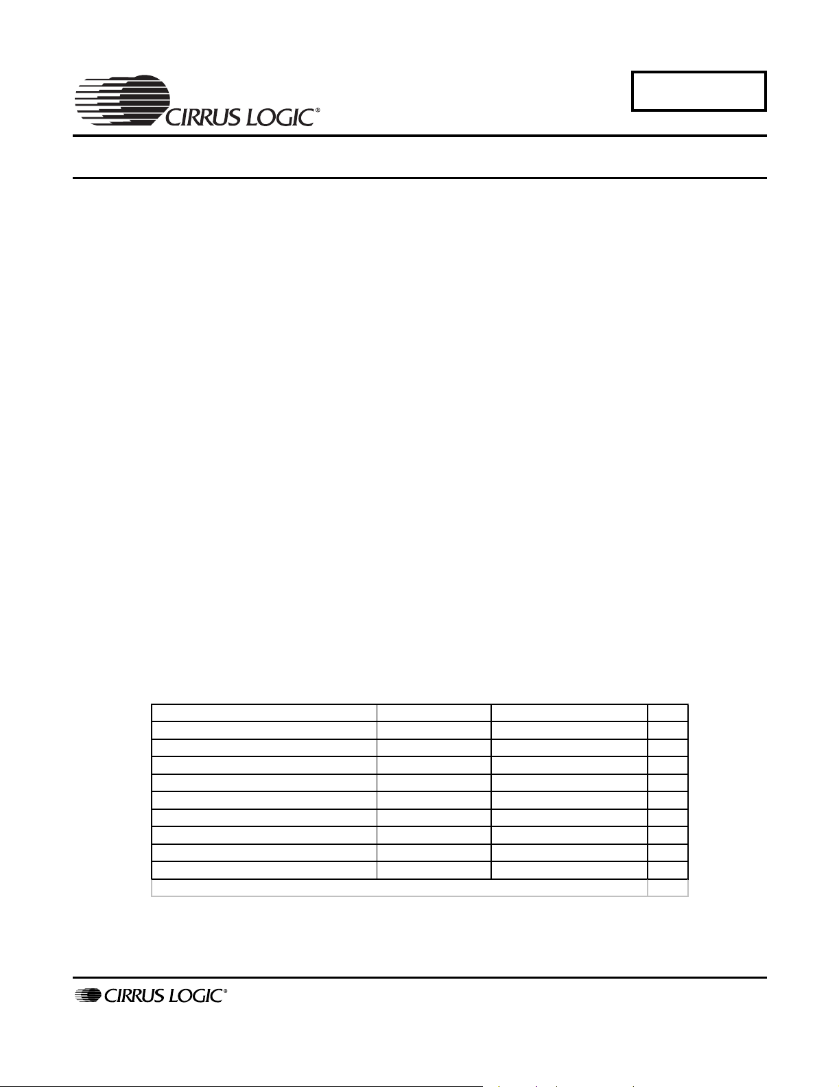
2. Key Specifications
Table 1 shows a comparison of the key specifications of these two devices, and Table 2 shows the pin
comparison between the CS5333 and the CS5340. Although these two devices are not pin compatible,
they are very similar in terms of overall functionality and feature set. The CS5340 achieves higher analog
performance and supports a wider range of output sample rates, including 192 kHz. This additional performance is the main reason for the increased power consumption of the CS5340 rel ative to the CS5333.
Parameter CS5333 CS5340 Units
Conversion 24 24 Bits
Dynam ic Range (A -wei ghted)* 95 98 dB
THD +N* -88 -95 dB
Analog Core Power Supply (VA) +1.8 to +3.3 +3.3 to +5.0 V
Digital Core Power Supply (VD) Powered from VA +3.3 to +5.0 V
Digital Interface Power Supply (VL) +1.8 to +3.3 +1.8 to +5.0 V
Maximum Power* 31 100 mW
Maximum Sample Rate 100 200 k Hz
Pack ag e 16-pin TSS OP 16-pin TSS OP
* Al l pe rformance/ p ower m easurem ents taken wi t h al l suppl i es s e t to 3.3 V
Table 1. Comparison of Key Specifications
http://www.cirrus.com
Copyright © Cirrus Logic, Inc. 2004
(All Rights Reserved)
MAR ‘04
AN249REV1
1
Page 2
AN249
r
A
r
r
r
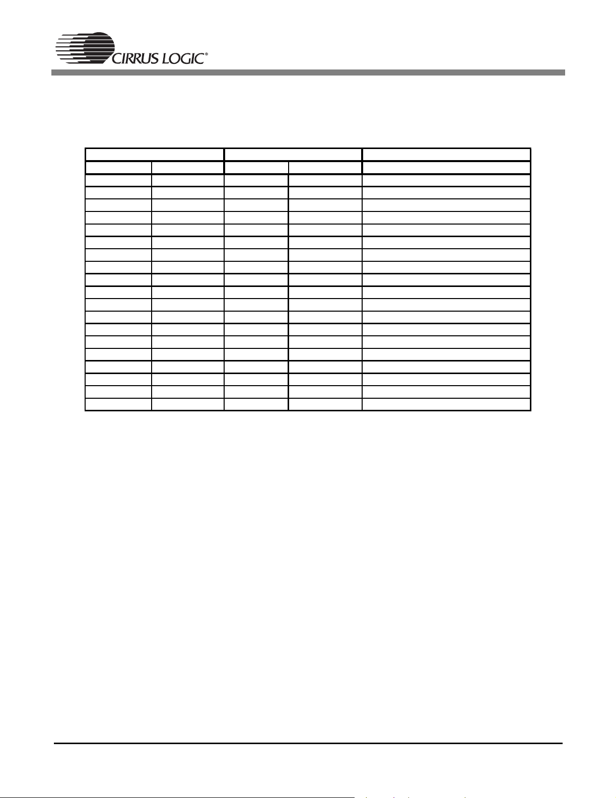
The CS5333 and CS5340 are both available in a 16-pin TSSOP package. As can be seen from Table 2,
all but three pins correlate directly in terms of functionality. These three pins account for a difference in
operational mode selection and a separate voltage supply pin for the CS5340 digital core.
CS5333 CS5340 Description
Pin Number Pin Name Pin Number Pin Name
1 VL 3 VL Logic Powe
2 MCLK 2 MCLK Master Clock
3 SCLK 7 SCLK Serial Clock
4 SDATA 4 SDOUT Serial Data
5VA13V
6 GND 5 GND Ground Reference
7 LRCK 8 LRCK Left/Right Clock
8 DIV - - Speed Mode Select/MCLK Divide
9 DIF - - Digital Interface Format Select
10 TST - - Test Pin
11 FILT+ 15 FILT+ Voltage Reference
12 REF_GND 14 REF_GND Ground Reference
13 AINR 12 AINR Right Channel Analog Input
14 AINL 10 AINL Left Channel Analog Input
15 VQ 11 VQ Quiescent Voltage Reference
16 RST 9 RST Reset
1 M0 Mode Selection
6 VD Digital Powe
16 M1 Mode Selection
Analog Powe
Table 2. Pin Compatibility Between the CS5333 and CS5340
2
Page 3
AN249
3. Typical Connection Diagrams
Figures 1 and 2 illustrate the typical connection diagram for the CS5333 and CS5340 respectively. The
analog and digital core of the CS5333 are powered from VA, which can be set from 1.8 V to 3.3 V. The
VL supply pin powers the digital interface logic from 1. 8 V to 3.3 V and can be set independently from VA.
1.8 V to 3.3 V
1.8 V to 3.3 V
+
.1µF
µF
1
1µF
1 µ
0
5
VA
11
FILT+
12
REF_GND
F
15
VQ
CS 5333
1
VL
RST
DIF
DIV
0
16
9
8
.1µF
+
Configuration
1
Mode
µF
Analog Input Filter
Figure 3
14
AINL
13
AINR
GND TST
6
10
Figure 1. CS5333 Typical Connection Diagram
MCLK
LRCK
SCLK
SDATA
2
7
3
4
47k
Digital
Audio
Source
Ω
Connect to:
• V L fo r Mas te r Mod e
• GND for Slave Mode
3
Page 4

AN249
The CS5340 has separate power supply pins for the analog and digital cores. The analog section is powered from the VA supply and the digital section is powered off of the VD supply. Both of these supply pins
can be powered from the same external source with a small series resistor between them for noise isolation. Both the analog and digital cores can operate independently from 3.3 V to 5.0 V. The VL pin of the
CS5340 supplies the digital interface logic, supports a wide opera ting range from 1.8 V to 5.0 V, and can
be powered independently from the VA and VD power supplies.
3.3 V to 5.0 V
3.3 V to 5.0 V
1 µ
1
1
1µF
F
µF
µF
+
+
.1µF
0
0
0
.1µF
0
.1µF
.1µF
15
14
11
13
VA
FILT+
REF_GND
VQ
*
Ω
5.1
CS5340
6
VD
3
VL
RST
M1
M0
0
* Resistor may only be
used if VD is derived from
VA. If used , do n o t driv e
any other logic from VD.
9
16
1
Configuration
1
Mode
µF
+
.1µF
1.8 V to 5.0 V
Analog Input Filter
Figure 4
10
AINL
12
AINR
GND
5
Figure 2. CS5340 Typical Connection Diagram
MCLK
LRCK
SCLK
SDOUT
2
10k
Digital
Audio
Source
Ω
Connect to:
• VL for I2S
• GND for L J
8
7
4
4
Page 5

AN249
4. Master/Slave and Speed Mode Selection
4.1 CS5333
In the CS5333, the selection for Master or Slave mode operation is determined by a resistor pull-up/pulldown on the SDATA pin (pin 4), as noted in Figure 1. If operating in Master mode, the Speed mode is
selected by the DIV pin (pin 8). If DIV is resistively pulled low, the CS5333 will enter into Base Rate mode
(Fs = 2 kHz to 50 kHz). If DIV is resistively pulled high to VL, the CS5333 will enter into High Rate mode
(Fs = 50 kHz to 100 kHz). If the CS5333 is operating in Slave mode, the Speed mode is auto-detected
and the DIV pin operates as an MCLK divide by two enable.
4.2 CS5340
In the CS5340, Master or Slave mode operation and Speed mode is determined by the mode pins, M1
and M0 (pins 16 and 1 respectively), as shown in Table 3.
M1 (Pin 16) M0 (Pin 1) Mode
0 0 Master, Single Speed Mode
0 1 Master, Double Speed Mode
1 0 Master, Quad Speed Mode
1 1 Slave, All Speed Modes
Table 3. CS5340 Mode Control
Please note that Base Rate mode is synonymous with Single Speed mode, and High Rate mode is synonymous with Double Speed mode.
5. Digital Interface Format Select
5.1 CS5333
The CS5333 supports both Left Justified and I
the DIF pin (pin 9). If this pin is held at a logic low upon startup, I
held at a logic high upon startup, Left Justified interface format will be selected.
5.2 CS5340
The CS5340 also supports both Left Justified and I
by a resistor pull-up/pull-down on the SDOUT pin (pin 4). If this pin is resistively pulled low upon startup,
Left Justified interface format will be selected. If this pin is resistively pulled high to VL upon startup, I
interface format will be selected.
2
S digital interface formats. The interface is selectable by
2
S digital interface formats. The interface is selectable
2
S interface format will be selected. If
2
6. System Clocking
The clocking requirements for the CS5333 and CS5340 are the same for Master mode operation. However, in Slave mode operation the CS5340 only supports a subset of the clocking supported in the
CS5333. The CS5333 supports an MCLK/LRCK ratio of 256x, 384x, 512x, and 768x in Base Rate mode
and 128x, 192x, 256x and 384x in High Rate mode. The CS5340 cannot support ratios of 192x, 384x, or
768x. See Table 4. Due to the auto-speed mode detect circuitry imple mented in the CS5340, not all sample rate ranges are supported in Slave mode. Please refer to the CS5340 datasheet for more information.
Device Speed Mode Supported MCLK/LRCK Ratios
CS5333 Base Rate 256, 384, 512, 768
High Rate 128, 192, 256, 384
CS5340 Single Speed 256, 512
Double Speed 128, 256
S
Ta ble 4. Supported MCLK/LRCK Ratios, Slave Mode Operation
5
Page 6

AN249
7. Input Filter Topology
Both the CS5333 and CS5340 implement a single-ended input architecture. Due to differences in the input
sampling topologies within the converters, the input filter requirements are different between these two
devices.
A suggested input filter topology for the CS5333 is shown in Figure 3. This input network consists of an
AC-coupling capacitor along with a single-pole lowpass filter.
CS5333
150 Ω
The CS5333 will self-bias the analog input node to the opti mal bias point (half of VA). The CS5333 implements an internal buffer on the analog input, reducing the amount of switching current on the input sampling node. This reduction in switching current makes the CS5333 less sensitive to series resistance on
the analog input lines.
0.47 uF
0.01 uF
C0G
Figure 3. CS5333 Input Filter
AINx
A suggested input filter topology for the CS5340 is shown in Figure 4.
634 Ω
100 kΩ
VA
100 kΩ
4.7 µF
100 kΩ
Figure 4. CS5340 Input Filter
470 pF
C0G
-
+
91 Ω
2200 pF
C0G
CS5340
AINx
This filter topology implements an external resistor-divider circuit to bias the output of the ampli fier to t he
optimal bias point (half of VA). Due to the internal architecture, the CS5340 requires low impedance on
the analog input lines. The topology shown in Figure 4 provides a sub-ohm input source impedance into
the CS5340 and isolates the input to the amplifier. For more information on this input filter topology, please
refer to the Application Note AN241.
A passive input filter can be used with the CS5340, however, the full analog performance of the CS5340
will not be realized. Figure 5 illustrates a unity gain, passive input filter solution and the resulting distortio n
performance. Please note that in this case the dynamic range performance of the CS5340 will not be limited by the input filter; only the distortion performance is affected.
6
Page 7

AN249
VA
CS5340
150 Ω
10 µF
100 kΩ
AIN
100 k
Ω
100 kΩ
2200 pF
C0G
-80
-85
d
-90
B
F
S
-95
-100
THD+N
Input = -1 dBFS
-105
20 20k50 100 200 500 1k 2k 5k 10k
Hz
Figure 5. CS5340 Passive Input Filter, Solution 1
7
Page 8

AN249
Some applications may require signal attenuation prior to the converter. The full-scale input vol tage of the
CS5340 will scale with the analog power supply voltage. For VA = 5.0 V, the full-scale input voltage is
approximately 2.8 Vpp, or 1 Vrms. Typical consumer audio line level outputs range from 1.5 to 2 Vrms.
Figure 6 shows a passive input filter for the CS5340 and the resulting THD+N over the audio bandwidth.
This filter provides 6 dB of signal attenuation. Due to the relatively high input impedance on the CS5340
analog inputs, the full distortion performance of the CS5340 cannot b e real ized. Also, the combination of
the series resistor and the biasing resistor-divider circuit will de termine the input impedance i nto the input
filter. In the circuit shown in Figure 6, the input impedance is approxima tely 5 kΩ. By doubling the resistor
values, the input impedance will increase to 10 kΩ. However, in this case the distortion performance will
drop to approximately 70 dB due to the increase in series resistance on the CS5340 analog inputs.
10 µF
2.5 k
VA
5 k
Ω
Ω
CS5340
AIN
100 k
Ω
-60
-62.5
-65
-67.5
-70
-72.5
-75
-77.5
-80
d
B
-82.5
F
-85
S
-87.5
-90
-92.5
-95
-97.5
-100
-
102.5
-105
20 20k50 100 200 500 1k 2k 5k 10k
5 kΩ
Hz
2200 pF
C0G
Figure 6. CS5340 Passive Input Filter, Solution 2
8
Page 9

AN249
8. Capacitor Size on the Reference Pin (FILT+)
The CS5340 and CS5333 require external capacitance on the internal reference voltage pin. For the
CS5333, the internal reference voltage is output on FILT+ (pin 11). On the CS5340, the FILT+ reference
voltage is output on pin 15. The size of the decoupling capacitor on this reference pin will affect the low
frequency distortion performance. The recommended solution for the CS5 333 is a 1
the FILT+ pin and analog ground. The recommended solution for the CS5340 is to use a 0.1
µ
in parallel with a 1
F capacitor for cost sensitive applications. See Figure 7 which illustrates the typical
low frequency distortion performance of the CS5340 with di ffere nt size capaci tors on the FILT+ reference
pin (pin 15). This plot was taken implementing the recommended input filter shown in Figure 4.
-70
-72
-74
-76
-78
-80
-82
-84
d
-86
B
-88
F
S
-90
-92
-94
-96
-98
-100
-102
-104
10 1k20 50 100 200 500
10 uF
22 uF
47 uF
1 uF
Hz
µ
F capacitor between
µ
F capacitor
Figure 7. CS5340 THD+N versus Frequency
9. Conclusion
The CS5340 is the recommended replacement for the CS5333, offering higher performance and 192 kHz
output sample rate capability. Special considerations must be made when upgrading designs to use the
CS5340 in place of the CS5333. These considerations include pin compatibility, functional mode selections, input filter design, and external capacitor requirements on the FILT+ reference pin.
9
Page 10

Revision Date Change
1 16 March 2004 Initial Release
AN249
Contacting Cirrus Logic Support
For a complete listing of Direct Sales, Distributor, and Sales Representative contacts, visit the Cirrus Logic web site at:
http://www.cirrus.com/
IMPORTANT NOTICE
Cirrus Logic, Inc. and its subsidiaries ("Cirrus") believe that the information contained in this document is accurate and reliable. However, the information
is subject to change without notice and is provid ed "AS IS" without warranty of any kind (express or implied). Customers are advised to obtain the latest
version of relevant informat ion to veri fy, before placing orde rs, that in formation be ing relied on is current and complete. All products are sold subject to
the terms and conditions of sale supplied at the time of order acknowledgment, including those pertaining to warranty, patent infringement, and limitation
of liability. No respon sib ili ty is a ss umed b y Ci rrus f or th e use o f thi s inf or mat ion , incl u ding us e of th is inf o rma tio n a s t he basis for manufacture or sale of
any items, or for infringement of pa tent s or other rights of thir d part ies. Th is doc ument is t he proper ty of C irrus an d by furn ishing this information, Cirrus
grants no license, express or implied under any patents, mask work rights, copyrights, trademarks, trade secrets or other intellectual property rights. Cirrus
owns the copyrights associated with th e info rmatio n co ntai ned he re in and giv es co nse nt for co pi es to be made of the info rmatio n only for use within your
organization with respect to Cirrus integrated circuits or other products of Cirrus. This consent does not extend to other copying such as copying for general
distribution, advertising or promotional purposes, or for creating any work for resale.
CERTAIN APPLICATIONS USING SEMICONDUCTOR PRODUCTS MAY INV OLVE POTENTIAL RISKS OF DEATH, PERSONAL INJURY , OR SEVERE PROPERTY OR ENVIRONMENTAL DAMAGE (“CRITICAL APPLICAT IO NS”). CIRRU S P RODUCTS A RE N OT D ESIGNED, AUTH ORIZED OR
WARRANTED FOR USE IN AIRCRAFT SYSTEMS, MILITARY APPLICATIONS, PRODUCTS SURGICALLY IMPLANTED INTO THE BODY, LIFE SUPPORT PRODUCTS OR OTHER CRITICAL APPLICATIONS (INCLUDING MEDICAL DEVICES, AIRCRAFT SYSTEMS OR COMPONENTS AND PERSONAL OR AUTOMOTIVE SAFETY OR SECURITY DEVICES). INCLUSION O F CIRRUS PRODUC TS IN SUCH AP PLICATIONS IS UNDERSTOOD
TO BE FULLY AT THE CUSTOMER'S RISK AND CIRRUS DISCLAIMS AN D MAKES NO WARRANTY, EXPRESS, STATUTORY OR IMPLIED, INCLUDING THE IMPLIED WARRANTIES OF MERCHANTABILITY AND FITNESS FOR PARTICULAR PURPOSE , WITH REGARD TO ANY CIRRUS
PRODUCT THAT IS USED IN SUCH A MANNER. IF THE CUSTOMER OR CUSTOMER'S CUSTOMER USES OR PER MITS THE USE OF CIRR US
PRODUCTS IN CRITICAL APPLICATIONS, CUSTOMER AGRE ES, BY SUCH USE, TO FULL Y INDEMNIF Y CIRRUS, ITS OFF ICERS, DIRECTORS,
EMPLOYEES, DISTRIBUTORS AND OTHER AGENTS FROM ANY AND ALL LIABILITY, INCL UDING ATTOR NEYS ' FEE S AN D COS TS, THAT MA Y
RESULT FROM OR ARISE IN CONNECTION WITH THESE USES.
Cirrus Logic, Cirrus, and the Cirr us Log ic logo de sign s are tr ademarks of Cirr us Log ic, Inc. All o ther br and and pr oduc t names in this d ocument ma y be
trademarks or service marks of their respective owners.
10
 Loading...