

Page 1
AN234
* Dynamic Range and THD+N specified with different input buffer topologies
AK5394A to CS5381 Conversion
by Kevi n L Tr etter
1. Introduction
The CS5381 is a complete analog-to-digital converter for digital audio systems. The CS5381 performs
sampling , analog- to-digital c onversion a nd anti-ali as filtering , generat ing 24-bit values for both left a nd
right chan nels.
The CS53 81 offers some unique advant ages over the A K5394A including:
- Over 70% REDUCTION in package size (TSSOP)
- 50% less power consumption
- Fewer external components required (See Section 2)
- Overflow detect
- Integrated level shifters
- Over 80% less group delay (48kHz output sample rate)
Table 1 sho w s a c om parison of the key specificat ions of these two devices.
AK5394A CS5381
Conversion (Bits) 24 24
Dynamic Range (A-weighted) dB 123* 120
THD+N dB -110* -110
Analog Core Power Supply (VA) V +5.0 V +5.0 V
Digital Core Power Supply (VD) +3.3 V to +5.0 V +3.3 V to +5.0 V
Digital Interface Power Supply (VL) N/A +2.5 V to +5.0 V
Maximum Power mW 870 348
Maximum Sample Rate kHz 216 200
Package
Table 1. Comparison of Key Specifications
28-pin SOP 24-pin SOIC/TSSOP
http://www.cirrus.com
Copyright Cirrus Logic, Inc. 2003
(All Rights Reserved)
JUL ‘03
AN234REV1
1
Page 2
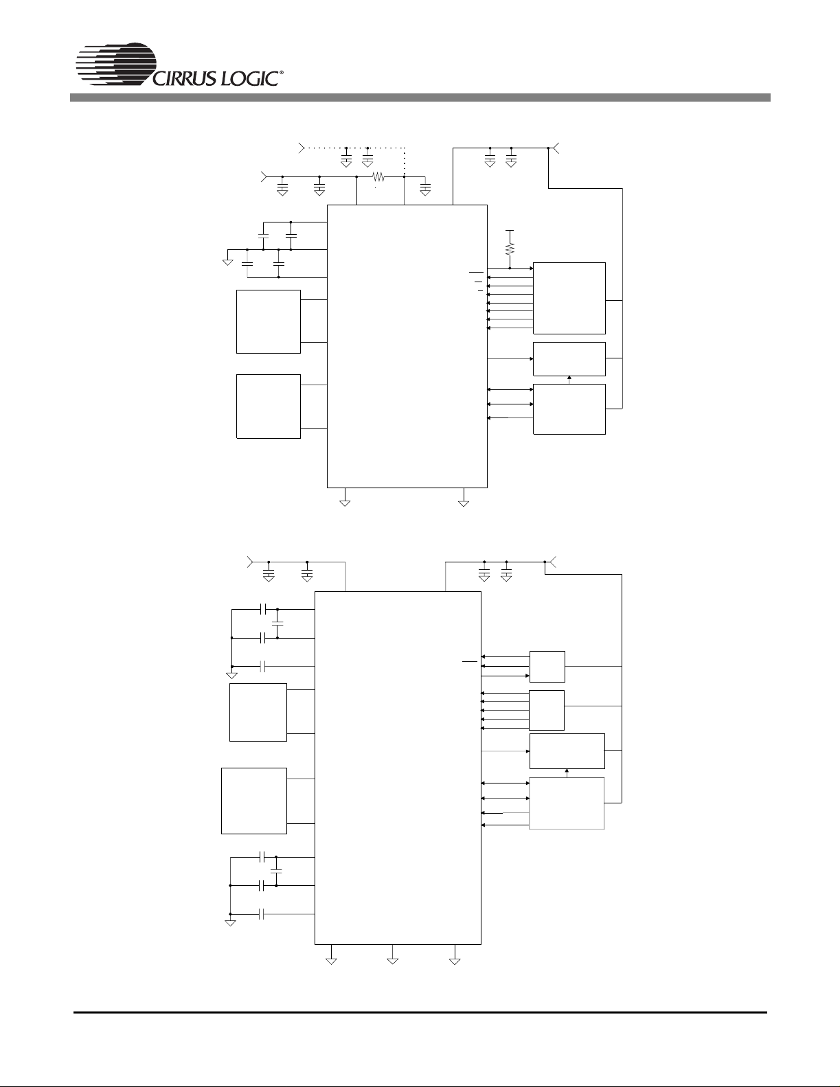
2. Typical Connection Diagrams
+5 V to 3.3 V
+5V
+
1µF
+
1µF 0.1µF
*
µ
0.1
F
Ω
5.1
AN234
+
µ
F
0.1
µF
0.1
1µF
+5V to 2.5V
D
CS5381
A/D CONVERTER
200 µ
F
1µF
+
Analog
(Sectio n 8)
Analog
(Section 8)
+
Input
Buffer
Input
Buffer
VA V
FILT+
0.1µF
REFGND
µ
0.1
F
VQ
AINL+
AINL-
AINR+
AINR-
GND
Figure 1. CS5381 Typical Connecti on Diagr am
+5V
+ +
10
*
+
C
*
+
C
0.22µF
Analog
Input
Buffer
(Section 8)
µF 0.1
0.1
µ
F
VA
VREFL+
0.22µF
VREFL-
VCOML
AINL+
A/D CONVERTER
AINL-
AK5394A
L
V
SDOUT
GND
D
V
ZCAL
HPFE
SMODE2
SMODE1
DFS0
DFS1
SDATA
OVFL
RST
2
I
S/LJ
M/S
HPF
MDIV
LRCK
SCLK
MCLK
µF
RST
CAL
M0
M1
VL
10 k
*
Resistor may only
be used if VD is
derived from VA. If
used, do not drive
any other logic
from VD.
µ
F
10
Reset and
Calibration
Power Down
and Mode
Settings
Audio Dat a
Processor
Timing Logic
and Clo ck
+5V to 3.3
Control
Mode
Control
Audio Data
Processor
V
Analog
Input
Buffer
(Section 8)
*
C
*
C
+
+
0.22µF
0.22µF
AINR+
AINR-
VREFR+
VREFR-
VCO MR
AGND
BGND
FSYNC
DGND
LRCK
SCLK
MCLK
* See Section 9
Timing Logic
andClock
Figure 2. AK5394A Typical Connecti on Diagram
2
Page 3
AN234
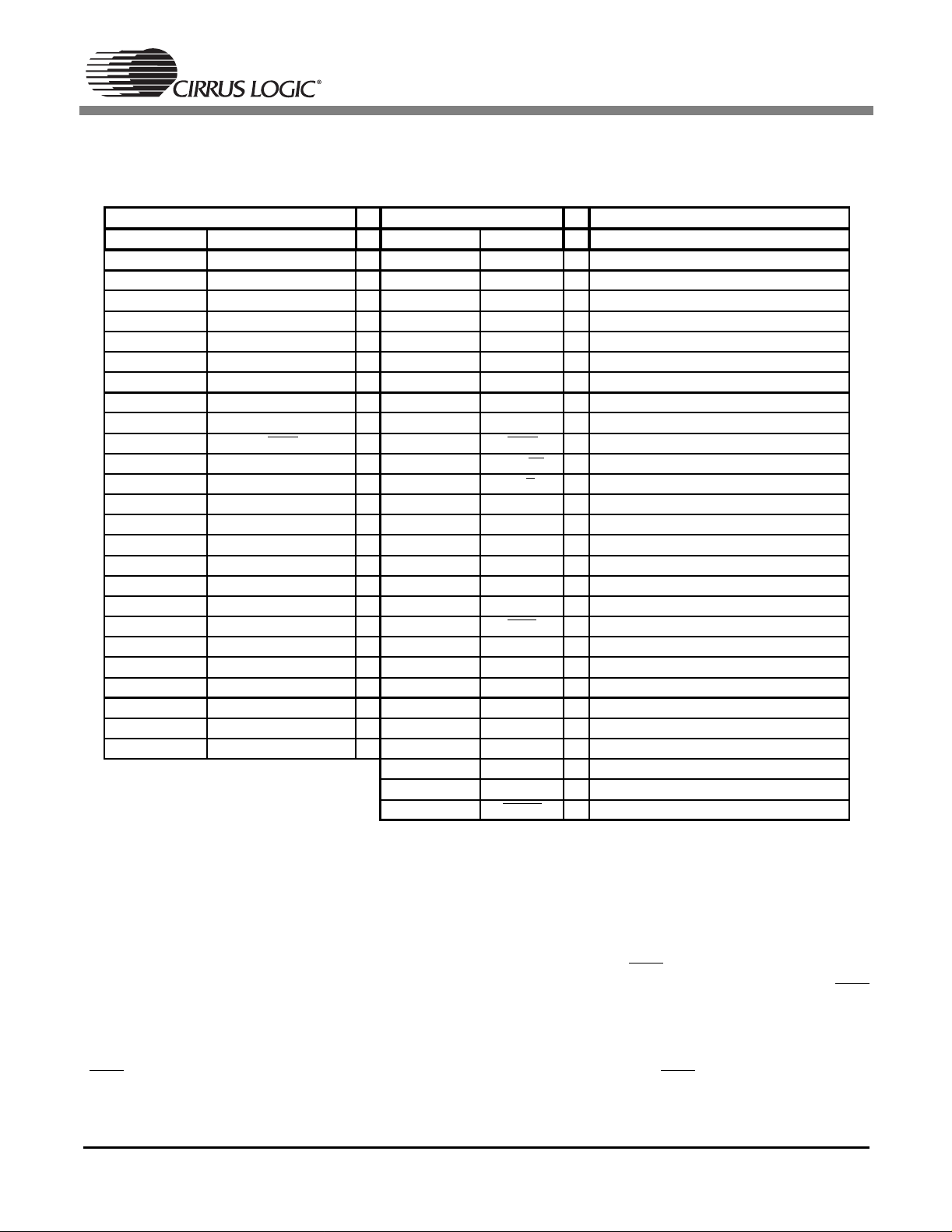
Pin Name
FILT+
Positive reference voltage
REFGND
Ground reference
VQ
Internal quiescent reference voltage
AINL+
Differential Left Channel Input
AINL-
Differential Left Channel Input
-
Zero Calibration Control
VD
Digital power
GND
Ground reference
-
Calibration Active Signal
RST
Reset
I2S/LJ
Digital Interface Format Select
M/S
Master/Slave Mode Select
LRCK
Left right clock
SCLK
Serial clock
SDOUT
Serial data
-
Frame Synchronization Signal
MCLK
Master clock
M0
Mode selection
HPF
High Pass Filter Enable
M1
Mode selection
-
Substrate Ground
GND
Ground reference
VA
Analog power
AINR-
Differential Right Channel Input
AINR+
Differential Right Channel Input
VL
Logic Power
MDIV
MCLK divider
15
OVFL
Overflow
3. Pin Compatibility
Table 1 sho w s th e pins of the AK5394A and the corresponding pins of the CS5381. Please not e that the
AK5394 A has 28 pins, and the CS5381 has 24 pins.
AK5394A CS5381 Description
Pin Number Pin Name Pin Number
1, 28 VREFL+, VREFR+ 24
2, 27 VREFL-, VREFR- 23
3, 26 VCOML, VCOMR 22
4 AINL+ 16
5 AINL- 17
6ZCAL 7VD 6
8DGND 7
9CAL 10 RST 1
11 SMODE2 12
12 SMODE1 2
13 LRCK 3
14 SCLK 4
15 SDATA 9
16 FSYNC 17 MCLK 5
18 DFS0 13
19 HPFE 11
20 DFS1 14
21 BGND 22 AGND 18
23 VA 19
24 AINR- 20
25 AINR+ 21
8
10
4. Offset Calibration
The CS5381, and AK5394A all have offset calibration capability. However, the calibration process varies
slightly bet w een the AK5394A and the CS5381.
4.1 CS5381
The CS53 81 implemen ts a high pass filter tha t can be controlled via the HPF
filter continuously subtracts a measure of the DC offset from the output of the decimation filter. If the HPF
pin is taken high during normal operation, the current value of the DC offset register is frozen and this DC
offset will c ontinue to be sub t rac t ed from the con v ersion result.
A system calibration can then be performed by first running the CS5381 with the high pass filter enabled
(HPF = LOW) until the filter settles. At this point, disable the high pass filter (HPF = HI), thereby freezing
the stored D C of f s et .
Table 2. Pin Compatibility Between AK5394A and CS5381
pin (pi n 11). The hi gh pass
3
Page 4

AN234
4.2 AK5394A
The AK5394A will automatically initiate a calibration sequence following a reset. The CAL pin (pin 9) is an
output that indicates when a calibration sequence is in progress. This calibration technique is very similar
to that des cr ibed above fo r th e C S5381.
The AK539 4A also has a ZCA L pin (p in 6) which a llows the calibrat ion input to be ob tained from eithe r
the analog input pins or the VCOM pins. The high pas s filter c an be controlled via the HP F E pin (pin 19).
In th e AK5394A , t he high p as s filter is either c ontinuously r unning or completely removed from the s ignal
path.
5. Master/Slave Selection and Digital Interface Format
The CS53 81 and AK 5394 A are pin c ompatib le in term s of sele cting Ma ster/Sl ave ope ration an d digitia l
interface f ormat. The pins match up as noted in Table 2.
6. Speed Mode Selection
The AK53 94 A su pport s thre e sp ee d mo des , “nor mal” , “do uble”, and “qu ad” a s det erm ined by t he D FS0
and DFS1 pins (pins 18 and 20 respectively). These pins are compatible with the M0 and M1 pins (pins
13 and 14 ) of t he CS5381, as s hown in Tabl e 2.
7. System Clock ing
The CS 538 1 i s fu l ly co mpat ibl e wit h t he cl ocki n g re qu ir emen ts of t he AK 53 94A. How ev er, t her e i s a sl igh t
difference when operating in Master mode. When operating in “normal” mode, the AK5394A will generate
an SCLK th at is 128×Fs. The CS5381 generates an SCLK that is 64×Fs.
The CS5 381 of fers a n inte gra ted MC LK d ivide r, w hich can b e con troll ed via the MD IV pin (pin 10 ). This
pin allows mu ltiple exte rna l MCL K/LR CK rat ios to b e su pp orte d. In o rde r to m ain tain co mpl ete c om pati bility betw een the AK5394A and the CS5381, conn ec t th e M D I V pin (pin 10) of the C S5381 to GN D .
8. Input Buffer Topology
The analog input buffers shown in Figures 9 and 10 of the AK5394A datasheet (dated January, 2002) will
also work fo r t he C S5381. In this c as e, th e “Bias” referenc e (in Figure 9) sh ould be sourced f r om the VQ
pin of the CS5381. However, these input buffers require a large input voltage level at the input to the buffer
and attenuate the signal prior to the converter. This much signal swing is not always possible in a real
system, and not necessary to achieve the full performance of the CS5381.
The follo win g se ctions co ntai n a d esc riptio n of a s ingle- en ded t o dif fere ntia l inpu t bu ffer (co mpa rable to
Figure 9 of the AK53 94A dat asheet) an d a fully different ial input buffer (co mparab le to Figure 10 of the
AK539 4A dat ashe et) . Thes e two buff er t opolo gie s are un ity gain , and ther efor e do not r ely o n a la rge i nput
voltage at the buffer input.
8.1 Single-Ended to Differential Input Buffer
Figure 3 shows a single-ended to differential analog input buffer. This buffer provides the proper biasing,
isolation from the switched capacitor currents, low output impedance, and anti-alias filtering. The second
op-a m p s tage is s et up in an in v ertin g c onfiguration to produce t he negative node of t he diff erent ial in put.
In the inpu t buffer show n below, the second stag e has unity ga in, and the single-end ed input level will
effectively be doubled when presented differentially to the converter. For example, a 2.8 Vpp single-ended input will provide a full-scale 5.6 Vpp differential input to the CS5381.
4
Page 5

100 kΩ
1
00 kΩ
3.3 kΩ
3.3 kΩ
3.3 kΩ
3.3 kΩ
1 µF
VA
1 µF
VA
470 pF
C0G
+
100 kΩ
0.01 µF 100 µF
470 pF
C0G
+
100 kΩ
0.01 µF 100 µF
634 Ω
634 Ω
634 Ω
634 Ω
91 Ω
91 Ω
470 pF
+
470 pF
+
C0G
C0G
634 Ω
634 Ω
91 Ω
91 Ω
2700 pF
C0G
0.01 µF1 µF
2700 pF
C0G
AN234
CS5381
AIN+
AIN-
VQ
AIN+
AIN-
Figure 3. Single-Ended to Differential Input Buffer
8.2 Fully Differential Input Buffer
Figure 4 sh ows a fully diffe rential analo g input buf fer. This buffer provides the proper bia sing, isolation
from the swit ched capac itor currents, low output impe dance, an d anti-alias fil tering. This inpu t buffer is
unity gain, so a 5.6 Vpp differential input will provide a full-scale 5.6 Vpp differential input into the CS5381.
634 Ω
100 kΩ
100 kΩ
100 kΩ
100 kΩ
10 µF
10 kΩ
10 kΩ
10 µF
10 µF
10 kΩ
10 kΩ
10 µF
0.01 µF
0.01 µF
470 pF
C0G
-
+
-
+
-
+
-
+
470 pF
C0G
470 pF
C0G
470 pF
C0G
91 Ω
634 Ω
91 Ω
634 Ω
91 Ω
634 Ω
91 Ω
1 µF
2700 pF
C0G
0.01 µF
2700 pF
C0G
CS5381
AIN+
AIN-
VQ
AIN+
AIN-
Figure 4. Fully Differential Input Buffer
5
Page 6

AN234
B
S
9. Capacitor Size on Reference Voltage Pin(s)
The CS 5381 a nd t he AK 53 94A bo th r equ i re e xte rn al c apa ci ta nce on th e in te rn al r e fer enc e v olt ag e p in( s) .
On the CS 5381 , th e inte rnal re feren ce v olta ge is outp ut on FILT + (pin 24). The A K539 4A has fo ur su ch
pins, VRE FL+ , VR EF L-, VRE FR-, and VRE FR + (p ins 1 , 2, 27, and 28 resp ectiv ely) . Ea ch o f thes e pi ns
require a large capacitor for noise decoupling. Please refer to Figure 12 of the AK5394A datasheet (dated
January , 2 002) for a plot of distortion v ers us frequen c y w it h v arious capac itor values on these reference
pins.
For co mpar ison , the s ame pl ot has be en gene rate d usi ng the CS5381 , as ca n be see n in Fi gur e 5. Ple ase
note that the CS5381 requires ONE such capacitor, while the AK5394A requires FOUR such capacitors.
CS5381 THD+N vs Frequency
-60
-70
-80
-90
d
F
-100
-110
-120
-130
10 20k20 50 100 200 500 1k 2k 5k 10k
220 µF
470 µF1000 µF
100 µF
-1dBFS Input
10 µF
Hz
Figure 5. CS5381 THD+N vs. Frequency
A compari son betw een Figu re 12 of the AK5 394A datash eet and the ab ove plot of the CS53 81 revea ls
that the CS53 81 ha s bett er low freq uenc y disto rtio n per forma nce f or a giv en ca paci tor va lue, and re quire s
only one capacitor as opposed to the four that are required for the AK5394A.
6
Page 7

AN234
C
F
h
I
C
n
i
t
v
o
t
n
o
f
a
s
g
s
o
r
o
l
d
A
in
t
a
n
t
t
C
-
V
R
W
-
P
-
S
D
T
-
C
S
P
S
P
,
E
Y
R
C
e
t
ontacting Cirrus Logic Support
or a complete listing of Direct Sales, Distributor, and Sales Representative contacts, visit the Cirrus Logic web site at:
ttp://www.cirrus.com/
MPORTANT NOTICE
irrus Logic, Inc. and its subsidiaries ("Cirrus") believe that the information contained in this document is accurate and reliable. However, the informatio
s subject t o change without notice and is provided "AS I S" without war ranty of any kin d (express or implied). Cus tomers are advised to obtain the lates
ersion of re levant inf orm ation t o veri fy, bef or e pla cing ord ers , tha t info rmat ion being relied on is c urren t an d com plete. Al l prod uc ts are sold subject t
he terms and conditions of sale supplied at the time of order acknowledgment, including those pertaining to warranty, patent infringement, and limitatio
f liability. No responsibility is assumed by Cirrus for the use of this information, including use of this information as the basis for manufact ure or sale o
ny items , or for infr i ngement of patents or other rights of third partie s. T his document is the pr operty of Cir rus and by fur ni s hing t his information, Cirru
rants no license, express or implied under any patents, mask work rights, copyrights, trademarks, trade secrets or other intellectual pr ope rt y ri ght s. Ci rru
wns the copyrights associated with the information contained herein and gives consent for copies to be made of the information only for use within you
rganization with respect to Cirrus integrated circuits or other products of Cirrus. This consent does not extend to other copying such as copying for genera
istribution, adverti sing or promot io nal purposes , or for creating any w ork for resale.
n export per mit ne eds t o be o btaine d from the c ompe tent autho rit ies of t he Jap ane se Gov ernm ent if any of the pro duct s or te chno lo gies desc ribe d
his material and controlled under the "Foreign Exchange and Foreign Trade Law" is to be exported or taken out of Japan. An export license and/or quot
eeds to be obtained from the competent authorities of the Chinese Government if any of the products or technologies described in this material is subjec
o the PRC Foreign Trade Law and is to be exported or taken out of the PRC.
ERTAIN APPLICATIONS USING SEMICONDUCTOR PRODUCTS MAY INVOLVE POTENTIAL RISKS OF DEATH, PERSONAL INJURY, OR SE
ERE PROPERTY OR ENVI RONMEN TAL DAMAG E ("C RITI CAL APPL ICA TIO NS") . CIR RU S PRODU CTS AR E NOT DESIG NE D, AU T HORI ZED O
ARRANTED FOR USE IN AIRCRAFT SYST EMS, MIL ITARY APPL ICATIO NS, PRODUCTS SUR GICALLY IMPL ANTED IN TO THE BODY, LI FE SUP
ORT PRODUCTS OR OTHER CRITICAL APPLICATIONS (INCLUDING MEDICAL DEVICES, AIRCRAFT SYSTEMS OR COMPONENTS AND PER
ONAL OR AUTOMOTIVE SAFETY OR SECURITY DEVICES). INCLUSION OF CIRRUS PRODUCTS IN SUCH APPLICATIONS IS UNDERSTOO
O BE FULLY AT THE CUSTOMER'S RISK AND CIRRUS DISCLAIMS AND MAKES NO WARRANTY, EXPRESS, STATUTORY OR IMPLIED, IN
LUDING THE IMPLIED WARRANTIES OF MERCHANTABILITY AND FITNESS FOR PARTICULAR PURPOSE, WITH REGARD TO ANY CIRRU
RODUCT THAT IS USED IN SUCH A MANNER. IF THE CUSTOMER OR CUSTOMER'S CUSTOMER USES OR PERMITS THE USE OF CIRRU
RODUCTS IN CRITICAL APPLICATIONS, CUSTOMER AGREES, BY SUCH USE, TO FULLY INDEMNIFY CIRRUS, ITS OFFICERS, DIRECTORS
MPLOYEES, DISTRIBUTORS AND OTHER AGENTS FROM ANY AND ALL LIABILITY, INCLUDING ATTORNEYS' FEES AND COSTS, THAT MA
ESULT FROM OR ARISE IN CONNECTION WITH THESE USES.
irrus Logic, Cirrus, and the Cirrus Logi c logo design s are trademarks of Cirrus Logi c, Inc. All other brand and product names in this document may b
rademarks or service marks of their respective owners.
7
 Loading...